Embed Size (px)
Citation preview
Four wave mixing at 1550 nm in siliconwaveguides:
enhancement and application
vorgelegt von
Dipl.-Ing-M.Sc. Andrzej Gajda
geb. in Szczecin
von der Fakultät IV - Elektrotechnik und Informatik der Technischen Universität Berlin
zur Erlangung des akademischen Grades
Doktor der Ingenieurwissenschaften-Dr.-Ing-
genehmigte Dissertation
Promotionsausschuss:Vorsitzender: Prof. Dr. Bernd TillackGutachter: Prof. Dr. Klaus PetermannGutachter: Prof. Dr. Juerg LeutholdGutachter: Dr. Lars Zimmermann
Tag der wissenschaftlichen Aussprache: 10. April 2017
Berlin 2017

Andrzej GajdaFour wave mixing at 1550 nm in silicon
waveguides:enhancement and application
Gratias autem Deo qui dat sapientiam

Acknowledgments
Even though it is unusual I would like to thank God for all the people that I havemet on the long and hard way towards PhD degree.
I would like to thank Prof. Petermann for giving me the opportunity to accomplishmy PhD in his research group in the institute ”Hochfrequenztechnik/Photonics”at the Technische Universitat Berlin. His guidance, support, encouragement andtechnical advises have been very precious.
I would like to express my appreciation to Dr. Lars Zimmermann, Prof. Bernd Tillack and Dr. Andreas Mai who gave me the opportunity to learn an advanced silicon photonics technology, and enabled possibility to fabricate the p-i-n waveguides and finish this thesis at IHP Microelectronics GmbH in Frankfurt(Oder). Advice and comments of Dr. Lars Zimmermann have been a great help in the development of this thesis.
I would like to acknowledge Dr. Jürgen Bruns who coordinated the project in the first part of the work. Here I would like to acknowledge all the people that contributed to the fabrication and measurements of the samples. My special thanks goes to Dave Stolarek and Hui Tian for their guidance in the process development and fabrication of the samples. I would like to thank Christian Mai, Dr. Dieter Knoll, Stefan Lischke for their advisory on samples production.
I have greatly benefited from Thomas Richter, Robert Elschner who helped withthe expertise on high power measurement setup and dr. Colja Schubert for supportwith high power devices that enabled building the measurement setup for char-acterization of the first samples. My appreciation goes to Dr. Francesco Da Ros,Dr. Dragana Vukovic and Prof. Christophe Peucheret for a very productive andjoyful time at the laboratory Danmarks Tekniske Universitet, even though I stilldid not manage to make sightseeing in Copenhagen. I would like to thank Dr.Mahmoud Al Jazayerifar and Giannino Dziallas for their support in numerical sim-ulations of four-wave mixing in silicon of insulator waveguides. I would like toacknowledge Dr. Benjamin Wohlfeil for the simulations of the grating couplers. Iam indebt to Georg Winzer for the late hours measurements and supporting dis-cussions, although he was sometimes right. I am deeply grateful to Ania Peczekwho patiently withstand my growing requests for the basic measurements on thesamples.
Here I would like to acknowledge all the colleagues for their kindness, helpfulness and the friendly atmosphere and the pleasant time we spent together. My spe-cial thanks goes to friends from IHP and TU Berlin: Ania Peczek, Despoina Petousi, David Stolarek, Georg Winzer, Mariana Cascalheira, Maurizio Cirillo, Marcin Brzozowski, Marcel Kroh, Ivano Giuntoni, Karsten Voigt, Benjamin Wohlfeil, Maurizio Cirillo, Jesus Gutierrez Teran and all the others who kindly supported me in every-day struggling with scientific and not scientific problems.
Last but not least I would like to thank to my family. Especially my beloved wifeMonika who gave me hand every time I thought I will never come to the end of thisthesis. Monika and my great kids Alicja and Miłosz helped me a lot to find the ev-eryday bright side of life. I would like to thank my parents Danuta and Jerzy Gajdaand grandparents Irena Gajda, Wacława and Bronisław Kaczynscy who constantly
5

asking for the progress in my thesis, did not allow me to even think about givingup. I am deeply grateful to my older sister Ola for her invaluable help in correctingthe thesis. I believe that the long hours we’ve spent on it made it easier to under-stand. I would like to thank all the members of my big family for encouraging meto pursue my goals.
Berlin, September 2016
6
Table of contents
Introduction 1
1 Background theory 51.1 Relevant properties of silicon material . . . . . . . . . . . . . 71.2 Propagation of light wave in silicon . . . . . . . . . . . . . . 10
1.2.1 Electrical susceptibility and polarization . . . . . . . 101.2.2 Propagation of light in silicon waveguide . . . . . . 121.2.3 Nonlinear Schrodinger equation (NLSE) and nonlin-
ear coefficient . . . . . . . . . . . . . . . . . . . . . . 141.2.4 Absorption and dispersion from free carriers and gen-
eration of free carriers by two photon absorption . . 151.2.5 Effective area . . . . . . . . . . . . . . . . . . . . . . . 161.2.6 Self phase modulation . . . . . . . . . . . . . . . . . 171.2.7 Cross phase modulation . . . . . . . . . . . . . . . . 181.2.8 Four-wave mixing . . . . . . . . . . . . . . . . . . . . 181.2.9 Four wave mixing simulation model . . . . . . . . . 22
2 Numerical simulations of the SOI waveguide for CW four wavemixing 252.1 Optical properties approximation of applied materials . . . 25
2.1.1 Linear absorption of bulk Si . . . . . . . . . . . . . . 252.1.2 Two photon absorption and free carriers absorption
induced by two-photon absorption . . . . . . . . . . 272.1.3 Material dispersion of silicon, silicon nitride and sil-
icon oxide . . . . . . . . . . . . . . . . . . . . . . . . 272.2 Optical properties of silicon nano-rib waveguide with lat-
eral p-i-n diode . . . . . . . . . . . . . . . . . . . . . . . . . . 292.2.1 Structure of the modeled waveguide . . . . . . . . . 302.2.2 Mode of the silicon nano-rib waveguide . . . . . . . 312.2.3 Dispersion in silicon nano-rib waveguides . . . . . . 322.2.4 Linear loss sources in a nano-rib waveguide with lat-
eral p-i-n diode . . . . . . . . . . . . . . . . . . . . . 342.2.5 Simulation of power dependent loss in silicon nano-
rib waveguides . . . . . . . . . . . . . . . . . . . . . 372.3 Simulations of CW four wave mixing in SOI waveguide . . 402.4 Reduction of free carrier lifetime . . . . . . . . . . . . . . . . 452.5 Electric simulations of free carrier lifetime in waveguide with
lateral p-i-n diode . . . . . . . . . . . . . . . . . . . . . . . . 47
7
TABLE OF CONTENTS
3 Design, fabrication and characterization of samples 553.1 Samples design . . . . . . . . . . . . . . . . . . . . . . . . . 563.2 Fabrication process . . . . . . . . . . . . . . . . . . . . . . . 58
3.2.1 Process design . . . . . . . . . . . . . . . . . . . . . . 583.2.2 Manufacturing . . . . . . . . . . . . . . . . . . . . . . 60
3.3 Characterization of fabricated nonlinear waveguides . . . . 613.3.1 Electrical and opto-electrical characterization of wa-
veguide based p-i-n diode . . . . . . . . . . . . . . . 623.3.2 Dispersion . . . . . . . . . . . . . . . . . . . . . . . . 633.3.3 Linear loss . . . . . . . . . . . . . . . . . . . . . . . . 653.3.4 Linear loss dependence on bias voltage in p-i-n wa-
veguides . . . . . . . . . . . . . . . . . . . . . . . . . 663.3.5 Power dependent loss due to TPA and FCA . . . . . 693.3.6 Continuous-wave four-wave mixing experiments . . 733.3.7 Phase sensitive amplification measurement . . . . . 873.3.8 Summary of Continuous Wave (CW) Four Wave Mix-
ing (FWM) and Phase Sensitive Amplification (PSA)measurement . . . . . . . . . . . . . . . . . . . . . . 91
4 System oriented experiments of wavelength conversion 934.1 All-optical wavelength conversion of the amplitude modu-
lated signal . . . . . . . . . . . . . . . . . . . . . . . . . . . . 944.2 Phase regeneration of DPSK modulated signals . . . . . . . 97
5 State of the Art 103
6 Conclusions 107
List of Acronyms and Chemical Symbols 111
List of symbols 113
List of used constants 118
Bibliography 119
List of figures 132
List of Publications 139
8
Introduction
Traffic in data communication networks has seen continuous growth overmany decades. Taking the example of transport networks we observe agrowth rate of about 60% per year in capacity. The increase in traffic issupported by various technologies but mainly driven by application re-lated to social media, moving images, internet of things etc. An importantcontender for future increase of fiber optical network capacity is opticalsignal processing. Work on optical signal processing has developed overmany decades, but only recently the integration platforms for optical sig-nal processing have attracted increased attention. Nevertheless many non-linear platforms for integrated optical signal processing are incompatiblewith the two major platforms for photonic and photonic-electronic inte-gration which are indium phosphide and silicon. The platforms’ maturityis an issue, because the main drivers behind the technological progressof the integrated photonic platforms are the common optical network ap-plications such as coherent transmission, low cost optical links for datacenters or switches. There is consensus that future growth of Internet willrequire photonic and photonic-electronic integration. Therefore it wouldbe desirable to make use of the major platforms for nonlinear optical signalprocessing.
The work presented in this thesis was performed in the framework of alarger research project concerning the nonlinear optical signal processingon the silicon-on-insulator platform. Within this project different conceptswere developed by several partners. Among others the particular projectsfocused on the following key issues: crystalline silicon, amorphous siliconand electro-optical polymers nonlinearity.
This thesis reports on the optical properties and numerical simulations ofthe silicon-on-insulator waveguide for continuous-wave four wave mix-ing. Moreover, it discusses the process of design, fabrication and character-ization of samples. The purpose of the research activities was to constructan appropriate silicon waveguide supporting the FWM at the wavelengthsaround 1550 nm. The CW FWM can be used for the amplification of thesignal, phase conjugation and wavelength conversion. Moreover, it can beuseful for applications such as optical sampling, channel demultiplexing,pulse generation and high speed optical switching [1].
First of all the choice of silicon as a nonlinear optical material platform ismotivated. Next the optical properties of the applied materials were set. Itwas a preparatory stage to establish the optical properties of silicon nano-rib waveguide with lateral p-i-n diode. The mode field and an effective
1
INTRODUCTION
index of the silicon waveguide were determined with the optical simula-tions. Next, the dispersion of the waveguide was calculated consideringdifferent materials covering the waveguide. The problem of the free car-riers accumulating in the waveguide rib was identified. According to theresearch of other authors in the past the p-i-n junction was proposed as anappropriate solution to this problem. The electrical simulations allowed toadapt the diode presented in the literature to the chosen waveguide geom-etry. The simulation of the nonlinear optical effects defined the directionof the design process. Next, the samples were fabricated in the BiCMOSpilot line at IHP GmbH.
Following the design and the fabrication process, the properties of the con-structed waveguides with the lateral p-i-n diode were characterized. Atfirst the linear loss of the waveguide was measured together with the lossand the bandwidth of the grating couplers. The latter were used for the in-and out-coupling light from the optical fiber to the waveguide. The opticalloss from the free carriers was observed in the waveguide even for the lowpower of the light. This effect was also subject to the research within thisproject being the subject of this thesis.
Once the samples were optically and opto-electrically characterized, it wasresearched whether the constructed silicon with the lateral p-i-n diode canbe used in the fiber optic communication system. In the first experimentsession the wavelength conversion efficiency and the quality of the con-verted signal were tested. In the second experiment session it was investi-gated if, the phase of the differential phase shift keying Differential PhaseShift Keying (DPSK) signal can be regenerated, using the waveguide de-veloped in this research project.
The research project was founded by Deutsche Forschung Gemeinschaft(DFG) and was realized in cooperation between Technische UniversitaetBerlin (TUB) and Institute for High Performance Microelectronics (IHP) inFrankfurt(Oder) within the Joint Lab Silicon Photonics. The first character-ization measurements were conducted with the support of the FraunhoferHeinrich Herz Institut Fraunhofer Heinrich Herz Institute (HHI). The sec-ond characterization session was performed at the Danske Tekniske Uni-versitet (DTU). Also there it was checked if the constructed silicon wave-guides can be used in the fiber optic telecommunication system aroundthe wavelength 1550 nm.
Number of people contributed to the work conducted in this researchproject. Mahmoud Jazayerifar and Gianino Dziallas created the tool for
2
the simulations of the FWM in the silicon waveguide. Benjamin Wohlfeilsimulated the influence of the p and n doped regions on the optical lossof the silicon waveguide using JCM Wave software. The samples fab-rication process at Innovation for High Performance Institute IHP wascoordinated by David Stolarek. The Fraunhofer Heinrich Herz Institutesupported the first measurement session with the necessary experimentalhardware. The measurements performed at DTU were a joint experimen-tal effort where the most of work was done by Francesco Da Ros, DraganaVukovic, Christophe Peucheret and the author of this thesis.
In the thesis there are six chapters. Chapter 1 introduces the necessarybackground theory used in the design of structures. It starts with the com-parison of the silicon material with the other possible nonlinear materialplatforms. Next the theoretical background is introduced for the followingeffects: the self phase modulation, cross phase modulation and four-wavemixing in silicon waveguide. Then we investigate optical properties of ma-terials used in waveguide fabrication process with special attention givento dispersion and excess loss.
In chapter 2 the numerical simulations are described. At first the modelsof the optical properties of applied materials were discussed. Then thesimulations of the following effects in a silicon waveguide are explained:mode profile, dispersion, linear and nonlinear loss, dispersion and CWfour wavemixing. Later the electrical properties of a p-i-n diode lateral tothe waveguide are discussed.
Chapter 3 presents realization and measurements of the silicon nano-rib p-i-n waveguide. The characterization of the samples covers linear loss mea-surements, power dependent loss measurements, current-voltage char-acteristics of the p-i-n diode, determination of Two Photon Absorption(TPA), FWM conversion efficiency, PSA that will be used in chapter 4 forrealization of phase regeneration.
The fourth chapter 4 discusses advanced measurements of the feasibilityof the p-i-n nano-rib waveguide for system applications. In this part ofthe thesis wavelength conversion of the 40 Gbps signal shall be demon-strated with a negligible power penalty of 0.2 dB due to applied 20V re-verse bias voltage. The second system measurement utilized FWM basedphase sensitive amplification of p-i-n silicon nano-rib waveguide, in orderto dynamically regenerate 10 Gbps differential phase shift keying (DPSK)signal.
Chapter 5 reports on the state of the art in the CW FWM conversion effi-
3

INTRODUCTION
ciency, and showing the achievements of this research. The different ap-proaches to avoid the free carriers absorption problem are discussed thereas well.
In the sixth chapter the conclusions of the research project are summarizedand recommendations for the future are outlined.
4
1Background theory
The optical waveguides need to fulfill certain requirements to supportfour-wave mixing (FWM). At first in this chapter it will be discussed whysilicon was chosen as a nonlinear material platform. The number of pa-rameters will be introduced in order to compare the chosen Silicon OnInsulator (SOI) platform with the other major platforms used for the samepurpose. Moreover, the relevant properties of the silicon material and thewaveguide structure shall be introduced. The silicon (Si) material was se-lected as the most appropriate for this research project. Furthermore, inthis chapter, it is explained how to achieve the enhancement of the FWMby adjusting waveguide geometry. Electrical and optical approaches areused separately since, at the time of preparation of this thesis, there wasno available software to model both at once.
Reason for the choice of silicon
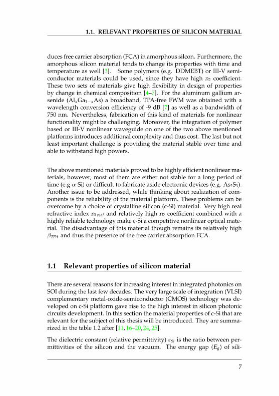
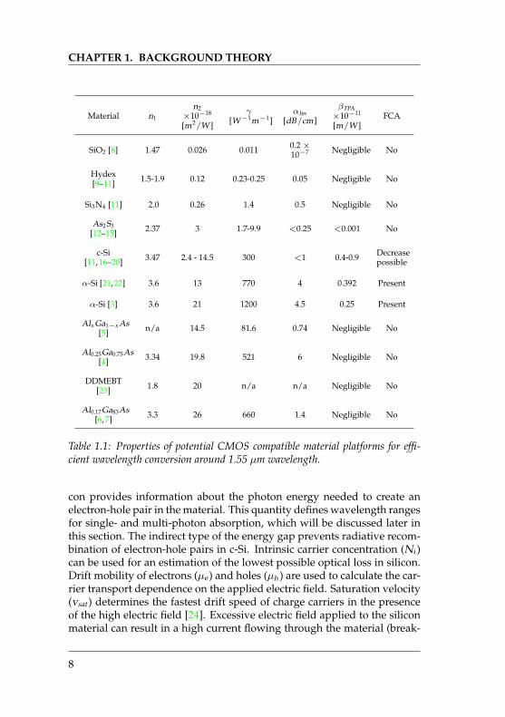
Many material platforms were examined for the nonlinear optical effcts.Table 1.1 presents a selection of the so calledχχχ(3) material platforms. It wasexamined which of them can be applied to obtain the optical Kerr effectaround 1550 nm. Below, the material parameters relevant for the choice ofthe nonlinear platform are briefly discussed. A more detailed explanationof these quantities will be performed later in the thesis. The integration ofphotonic devices requires a light confinement on a sub-micron area. Thiscan be realized only with the high real linear refractive index n1real , thuscreating the structures with high refractive index contrast (). The real part
5
CHAPTER 1. BACKGROUND THEORY
of the nonlinear refractive index n2, known as well as Kerr coefficient, tellshow much the refractive index of the medium changes with the optical in-tensity of the propagating light. The nonlinear coefficient γ results fromboth: the linear refractive index and the nonlinear refractive index. Thehigher are n1real and n2, the higher can be γ. Vital parameters of the non-linear optical material are the optical loss parameters αlin and βTPA . In ta-ble 1.1, the αlin is the reported in the literature state-of-the-art linear loss ofthe realized nonlinear wave-guiding structures. The two photon absorp-tion βTPA , is a TPA coefficient related to the intensity of the guided light.The two photon absorption results from the simultaneous absorption oftwo photons by the material with the exitation of the atom or the moleculeto the higher energy level [2]. In silicon it results in a generation of anelectron-hole pair. The detrimental influence of the Free Carrier Absorp-tion (FCA) is also presented in the table 1.1. In other materials, includedin table 1.1 the βTPA and FCA are negligible.
The obvious solution in the case of a fiber optic system would be apply-ing a silica (silicon dioxide (SiO2)) waveguide. With the advantages ofthe high coupling efficiency and the low linear propagation loss, the SiO2
material could be easily incorporated in a fiber optic system. However,these waveguides have a large cross-section due to the low refractive in-dex. Moreover, the low Kerr coefficient (n2) requires a structure with thelength of several hundred meters, in order to exhibit high nonlinear effect.Shorter structures can be achieved when using a material with a higherrefractive index like called Hydex [19, 20]. Waveguides made of this ma-terial perform with a low linear and nonlinear loss. At the same time Hy-dex have ten times larger n2 nonlinearity than SiO2. Due to its proprietarycomposition, the material is relatively little reported in the literature. A sil-icon nitride (silicon nitride (Si3N4)) material is another material platformknown for the nonlinear optical effects. It performs with the higher n1real
and n2 than in Hydex and can be used to produce a low loss waveguide.However a Si3N4 waveguide still needs to be relatively long to provide anefficient nonlinear interaction.
Another step in the minimization of the nonlinear waveguide dimensionsand increase in nonlinear parameters might be possible with arsenic sul-fide (As2S3). The material enabling further decrease in the length of thenonlinear structures is amorphous silicon (α-Si). Its high n0 and high n2
allows for a strong light confinement in the small waveguide cross-section,and thus short structures. However, the nonlinear interaction efficiencyin this material is affected by a high αlin and (TPA). Moreover the TPA in-
6
1.1. RELEVANT PROPERTIES OF SILICON MATERIAL
duces free carrier absorption (FCA) in amorphous silcon. Furthermore, theamorphous silicon material tends to change its properties with time andtemperature as well [3]. Some polymers (e.g. DDMEBT) or III-V semi-conductor materials could be used, since they have high n2 coefficient.These two sets of materials give high flexibility in design of propertiesby change in chemical composition [4–7]. For the aluminum gallium ar-senide (Alx Ga1−x As) a broadband, TPA-free FWM was obtained with awavelength conversion efficiency of -9 dB [7] as well as a bandwidth of750 nm. Nevertheless, fabrication of this kind of materials for nonlinearfunctionality might be challenging. Moreover, the integration of polymerbased or III-V nonlinear waveguide on one of the two above mentionedplatforms introduces additional complexity and thus cost. The last but notleast important challenge is providing the material stable over time andable to withstand high powers.
The above mentioned materials proved to be highly efficient nonlinear ma-terials, however, most of them are either not stable for a long period oftime (e.g α-Si) or difficult to fabricate aside electronic devices (e.g. As2S3).Another issue to be addressed, while thinking about realization of com-ponents is the reliability of the material platform. These problems can beovercome by a choice of crystalline silicon (c-Si) material. Very high realrefractive index n1real and relatively high n2 coefficient combined with ahighly reliable technology make c-Si a competitive nonlinear optical mate-rial. The disadvantage of this material though remains its relatively highβTPA and thus the presence of the free carrier absorption FCA.
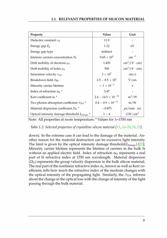
1.1 Relevant properties of silicon material
There are several reasons for increasing interest in integrated photonics onSOI during the last few decades. The very large scale of integration (VLSI)complementary metal-oxide-semiconductor (CMOS) technology was de-veloped on c-Si platform gave rise to the high interest in silicon photoniccircuits development. In this section the material properties of c-Si that arerelevant for the subject of this thesis will be introduced. They are summa-rized in the table 1.2 after [11, 16–20, 24, 25].
The dielectric constant (relative permittivity) εSi is the ratio between per-mittivities of the silicon and the vacuum. The energy gap (Eg ) of sili-
7
CHAPTER 1. BACKGROUND THEORY
Material n1
n2×10−18
[m2/W ]
γ[W−1m−1]
αlin[dB/cm]
βTPA×10−11
[m/W ]FCA
SiO2 [8] 1.47 0.026 0.011 0.2 ×10⁻⁷ Negligible No
Hydex[9–11] 1.5-1.9 0.12 0.23-0.25 0.05 Negligible No
Si3N4 [11] 2.0 0.26 1.4 0.5 Negligible No
As2S3[12–15] 2.37 3 1.7-9.9 <0.25 <0.001 No
c-Si[11, 16–20] 3.47 2.4 - 14.5 300 <1 0.4-0.9 Decrease
possible
α-Si [21,22] 3.6 13 770 4 0.392 Present
α-Si [3] 3.6 21 1200 4.5 0.25 Present
Alx Ga1−x As[5] n/a 14.5 81.6 0.74 Negligible No
Al0.25Ga0.75As[4] 3.34 19.8 521 6 Negligible No
DDMEBT[23] 1.8 20 n/a n/a Negligible No
Al0.17Ga83As[6, 7] 3.3 26 660 1.4 Negligible No
Table 1.1: Properties of potential CMOS compatible material platforms for effi-cient wavelength conversion around 1.55 µm wavelength.
con provides information about the photon energy needed to create anelectron-hole pair in the material. This quantity defines wavelength rangesfor single- and multi-photon absorption, which will be discussed later inthis section. The indirect type of the energy gap prevents radiative recom-bination of electron-hole pairs in c-Si. Intrinsic carrier concentration (Ni )can be used for an estimation of the lowest possible optical loss in silicon.Drift mobility of electrons (µe ) and holes (µh ) are used to calculate the car-rier transport dependence on the applied electric field. Saturation velocity(vsat ) determines the fastest drift speed of charge carriers in the presenceof the high electric field [24]. Excessive electric field applied to the siliconmaterial can result in a high current flowing through the material (break-
8
1.1. RELEVANT PROPERTIES OF SILICON MATERIAL
Property Value Unit
Dielectric constant εSi 11.9 -
Energy gap Eg 1.12 eV
Energy gap type indirect -
Intrinsic carriers concentration Ni 9.65 × 109 cm−3
Drift mobility of electrons µe 1.450 cm2/(V · cm)
Drift mobility of holes µh 500 cm2/(V · cm)
Saturation velocity vsat 1 × 107 cm/s
Breakdown field EBD 2.5 − 8.5 × 10⁵ V/cm
Minority carrier lifetime ∼ 1 × 10⁻³ s
Index of refraction nSi * 3.47 -
Kerr coefficient n2 * 2.4 − 14.5 × 10⁻¹⁸ m2/W
Two photon absorption coefficient βTPA * 0.4 − 0.9 × 10⁻¹¹ m/W
Material dispersion coefficient DSi * −0.875 ps/(nm · m)
Optical intensity damage threshold Idamage * 1 − 4 GW/cm2
Note: All properties at room temperature; * Values for λ=1550 nm
Table 1.2: Selected properties of crystalline silicon material [11, 16–20, 24, 25].
down). In the extreme case it can lead to the damage of the material. An-other reason for the material destruction can be excessive light intensity.The limit is given by the optical intensity damage threshold(Idamage ) [25].Minority carrier lifetime represents the lifetime of carriers in the bulk Siwithout an applied electric field. Index of refraction nSi represents a realpart of Si refractive index at 1550 nm wavelength. Material dispersion(DSi ) represents the group velocity dispersion in the bulk silicon material.The real part of the nonlinear refractive index n2, known as well as Kerr co-efficient, tells how much the refractive index of the medium changes withthe optical intensity of the propagating light. Similarly, the βTPA informsabout the change in the optical loss with the change of intensity of the lightpassing through the bulk material.
9
CHAPTER 1. BACKGROUND THEORY
1.2 Propagation of light wave in silicon
Propagation of light in dielectrics is in general described by Maxwell’sequations. Considering a homogeneous medium and an electromagneticwave propagating in it, the Maxwell’s equations can be used to derive thewave equation [1, 26]:
∇×∇× E +1c2
∂2E∂t 2 = −µ0
∂2P∂t 2 (1.1)
where E is the electric field , P is the electric polarization, µ0 is the vacuumpermeability and c represent the speed of light in vacuum.
1.2.1 Electrical susceptibility and polarization
The theoretical analysis of an interaction of light with the cristalline sili-con has already been thoroughly performed in [26–29]. The electromag-netic wave propagating through the material causes the displacement ofthe bound electrical charges D, proportional to the electric field E(r, t ) andthe electric polarization of the medium P [27, 30]:
D = ε0εSi E = ε0 (1 +χχχ) E ≡ P + ε0E (1.2)with vacuum permittivity ε0, relative silicon permittivity εSi and electricfield E. The electric polarization P(r, t ), induced by the electric field, wherer and t are the position and the time respectively. The electric polarizationP can be generally expressed by the power series of the electric field [27,28]:
P = D − ε0E = ε0(χχχ(1) · E +χχχ(2) : EE +χχχ(3)...EEE + ...) (1.3)
with the ith-order susceptibility χχχ(i ) expressed by (i+1)th-rank tensor andthe electric field E (r, t ). From the equation (1.3), the two components ofthe polarization, the linear PL and the nonlinear PNL [27, 28] can be ex-tracted:
PL = ε0χχχ(1) · E (1.4)
PNL = ε0
(χχχ(2) : EE +χχχ(3)...EEE + ...
)(1.5)
10
1.2. PROPAGATION OF LIGHT WAVE IN SILICON
The linear part of the susceptibility χχχ(1), which in general is complex, gov-erns effects such as dispersion and linear absorption or amplification. Thelinear complex refractive index n1 = n1real + in1imag is related to first ordersusceptibility by [31, 32]:
n12 = 1 + (χχχ(1)) (1.6)
and thus
n12real − n1
2imag = 1 + Re(χχχ(1)) (1.7)
2n1imag n1real = Im(χχχ(1)) (1.8)
Silicon is an anisotropic and dispersive material and hence theχχχ(1) is a ten-sor, where each component is the function of a wavelength. Additionally,silicon is a centrosymmetric material, and thus the second order suscepti-bility vanishes (χχχ(2) ≡ 0) [27]. The lowest order nonlinearity in Si becomesthen the third order nonlinearity. Therefore, the nonlinear polarization canbe defined as follows:
PNL ≈ ε0χχχ(3)E3 (1.9)
The assumptions of the following calculations are set below (as in [27]).Firstly, only the Kerr effect and the TPA contribution to the nonlinear po-larization is taken into account. Moreover, it is considered that the light ismonochromatic and linearly polarized. Thus isotropic approximation canbe used. The Kerr and TPA effects have a response time of tens of fem-toseconds, providing effectively instantaneous response to electric fieldvariation. These effects are commonly described by a nonlinear refrac-tive index n2 and two photon absorption coefficient βTPA , that are relatedto nonlinear susceptibility χχχ(3) [27]:
n2 =3
4ε0cn12real
Re(χχχ(3)eff ) (1.10)
βTPA =3ω
2ε0c2n12real
Im(χχχ(3)eff ) (1.11)
where the χχχ(3)eff is given, for the crystal orientations, which are relevant for
the research project ⟨100⟩, ⟨110⟩ and ⟨111⟩ by [27, 30]:
11
CHAPTER 1. BACKGROUND THEORY
χ(3)⟨100⟩eff = χ(3)
1111 (1.12)
χ(3)⟨110⟩eff =
12
(χ(3)1111 + 3χ(3)
1122) (1.13)
χ(3)⟨111⟩eff =
13
(χ(3)1111 + 6χ(3)
1122) (1.14)
Lin et al. in [30], proved experimentally that proportionality χ(3)1111 =
2.36χ(3)1122 occurs in the range of wavelengths from 1.2 to 2.4 µm . This
leads to simplified form of the formulas (1.13) and (1.14):
χ(3)⟨110⟩eff = 1.1356χ(3)
1111 (1.15)
χ(3)⟨111⟩eff = 1.1808χ(3)
1111 (1.16)
The formulas (1.15) and (1.16) suggest that the preferred direction for thebest nonlinear optical Kerr interaction would be ⟨111⟩. In practice, how-ever, the commonly available SOI substrates are perpendicular to the crys-tal direction ⟨001⟩ and the waveguiding structures are fabricated mostlyalong the crystal direction [110]. Orientation of the waveguide in respectto the crystal directions is shown in figure 2.5).
1.2.2 Propagation of light in silicon waveguide
nwg
ncl
Dwg
Dcl
Dsub
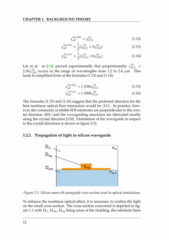
Figure 1.1: Silicon nano-rib waveguide cross-section used in optical simulations
To enhance the nonlinear optical effect, it is necessary to confine the lighton the small cross-section. The cross-section concerned is depicted in fig-ure 1.1 with Dcl , Dsub , Dwg being areas of the cladding, the substrate (here
12
1.2. PROPAGATION OF LIGHT WAVE IN SILICON
it is just a layer under the waveguide) and the waveguide respectively. Thetotal area Dtot contains all these areas. The materials have the refractive in-dices ncl , nwg and nsub correspondingly. For the sake of further simplifica-tion in calculations the change in P due to the propagating wave is treatedas a small perturbation. Moreover, we assume, that the linearly polarized,quasi-monochromatic optical field maintains its polarization during prop-agation along the medium (along the z direction). Under these conditions,the optical field can be separated in the transverse component and the lon-gitudinal components. Then it can be decomposed in the slowly varyingenvelope and the fast oscilating term at the frequency ω0 [1, 26]:
E = xFE (x , y , t )A (z , t ) ei(β(ω0)z−ω0t ) (1.17)
where x is a unity polarization vector, FE (x , y , t ) is a vectorial electrictransverse field distribution of the waveguide mode, A (z , t ) is the slowlyvarying amplitude, and β(ω0) is a mode propagation constant dependenton the frequency ω0. The slowly varying amplitude is defined so that|A (z , t )|2 is the average optical power. Similarly the magnetic field canbe expressed as follows [33]:
H = yFH (x , y , t )A (z , t ) ei(β(ω0)z−ω0t ). (1.18)
where FH (x , y , t ) is a vectorial magnetic field distribution in the trans-verse plane of the waveguide. The functions FE (x , y , t ) and FH (x , y , t )were calculated numerically with the full- vector mode solver developedby Fallahkhair et al. in Matlab environment and described in [34]. Resultsof the calculations are presented in the part considering the design of thestructure.
As the susceptibility χχχ is a function of ω, the refractive index n1real (or itsequivalent neff in media with the limited transverse dimensions) and β de-pend on the optical frequency. Following the references [1, 27] the disper-sion in the waveguide can be accounted for by the Taylor series expansionof the β around the center frequency ω0 as follows:
β(ω) = n1realω
c= β0 + β1(ω − ω0) +
12β2(ω − ω0)2 + ... (1.19)
where:
13
CHAPTER 1. BACKGROUND THEORY
βm =(
d mβ
dωm
)ω=ω0
(m = 1, 2, ...) (1.20)
the β1 and β2 are by definition expressed as follows [1]:
β1 =1
vg=
ng
c=
1c
(n1real + ω
dn1real
dω
), (1.21)
β2 =1c
(2
dn1real
dω+ ω
dn12real
dω2
)(1.22)
where vg and ng are the group velocity and the group index respectively.Physically vg represents the velocity of the optical pulse propagation whileβ2 is a group velocity dispersion responsible for the pulse broadening. Forconvenient comparison with the commonly used terms in fiber optics, fur-ther in the thesis, the dispersion coefficient will be defined as in [1]:
D =dβ1
dλ= −2πc
λ2 β2 = −λ
cd 2n1real
dλ2 (1.23)
1.2.3 Nonlinear Schrodinger equation (NLSE) and nonlinear co-efficient
In order to investigate the change of the amplitude A (z , t ) along the wa-veguide, the following Nonlinear Schrodinger Equation (NLSE) can be de-rived from the wave equation (1.1) [26]:
∂A∂z
= − αlin
2A +
(N∑
n=1
(−i)(n+1) βn
n!∂n
∂tn
)A + iγ|A |2A + ik0∆nFCD A+
− ∆αFCA
2A − βTPA
2Aeff|A |2A
(1.24)
where βn is n-th order dispersion term and γ is the nonlinear coefficientdefined as:
γ =k0n2
Aeff(1.25)
14
1.2. PROPAGATION OF LIGHT WAVE IN SILICON
the k0 = ω/c is the wave number, ∆nFCD and ∆αFCA are the change of therefractive index and the excess loss due to the presence of the free carriers(section 1.2.4). The effective area (Aeff ) is described more precisely later inthe thesis (section 1.2.5). Here the CW operation is considered, away fromthe zero group velocity dispersion wavelength. Additionally the frame ofreference moving at the the group velocity is used as in [1]:
τ ≡ t − β1z . (1.26)
Hence the equation (1.24) can be simplified as follows:
∂A∂z
= − αlin
2A − i
β2
2∂2A∂t 2 + iγ|A |2A +
n1real ik0∆nFCD
neff realA+
− n1real∆αFCA
2neff realA − βTPA
2Aeff|A |2A
(1.27)
where neff real represents a real part of a effective refractive index of thewaveguide.
1.2.4 Absorption and dispersion from free carriers and genera-tion of free carriers by two photon absorption
The free electrons and holes with densities Ne and Nh (both represented incm−3), respectively, cause the change in the loss and refractive index. Con-sidering wavelengths of around 1550 nm the loss change ∆αFCA (given incm−1 ) and the refractive index change ∆nFCD can be calculated accordingto the empirical formulas [27, 29, 35]:
∆nFCD = −(
8.8 · 10−4Ne + 8.5 · Nh0.8)× 10−18 (1.28)
∆αFCA = (8.5 · Ne + 6.0 · Nh ) × 10−18 (1.29)
In the TPA process, two photons simultaneously absorbed by silicon createa pair of free carriers. The number of photons taking part in this interactionis proportional to the square of power P 2 = |A |4 and the probablity ofTPA is governed by βTPA such that the average free carrier generation [36,37]
15
CHAPTER 1. BACKGROUND THEORY
GTPA
[cm3
s
]=
βTPA
2hωAeff2 |A |4 (1.30)
Moreover, it is assumed that the densities of electrons and holes generatedby TPA are equal (Ne = Nh = N ). Furthermore the recombination of freecarriers is governed by an effective carrier lifetime τeff (Eq. 1.31). Thisquantity is defined as the time necessary for the free carriers concentrationN (in cm−3) to decrease by 1/e [38]. Then the steady state free carriersdensity (dN/dt ) = 0 can be expressed along the propagation direction asN (z) = GTPA · τeff . In order to calculate the loss resulting from the TPAinduced excess FCA in CW operation, the corresponding loss coefficient istaken:
∆αFCA [cm−1] = (8.5 · N + 6.0 · N ) × 10−18 = σFCA · N = σFCA GTPAτeff
(1.31)with
σFCA [cm2] = 1.45 × 10⁻¹⁷ · (ωr/ω)2 (1.32)
Accordingly the influence of electrons and holes on the refractive indexchange was evaluated. Nevertheless, it was assumed that the impact ofthe holes on the refractive index change ∆nFCD is 5 times the influence ofelectrons, such that [29]:
∆nFCD = −(
6 · 8.8 · 10−4N)× 10−18 = σFCD × N = σFCD GTPAτeff (1.33)
withσFCD [cm3] = −5.3 × 10⁻²¹ · (ωr/ω)2 (1.34)
1.2.5 Effective area
In this thesis only the waveguide nonlinearity is considered, which is de-termined by properties of c-Si material. The nonlinearity of the surround-ing material was neglected as it is two orders of magnitude smaller andthe most of the light travels in the waveguide. In the optical calculationsperformed in the thesis the nonlinear coefficient γ was applied as in theequation (1.25). To calculate γ the effective area parameter Aeff must bedetermined. The effective area shall be understood as the relation of the
16
1.2. PROPAGATION OF LIGHT WAVE IN SILICON
power transported in the waveguide cross-section to the effective inten-sity. The effective intensity is by definition the intensity of the plane wavepropagating in the bulk homogeneous medium with the optical propertiesof the waveguide material [33]. Assuming the orthogonality of the trans-verse mode fields the effective area can be defined as follows [33]:
Aeff =c2µ0
2
nSi2
⏐⏐⏐∫∫DtotRe {FE (x , y) × FH (x , y)⋆} · ez dxdy
⏐⏐⏐2∫∫Dwg
|FE (x , y)|4 dxdy(1.35)
where the FE (x , y) and FH (x , y) are the vectorial electric and magneticmode profiles respectively, as given in formulas (1.17) and (1.18).
1.2.6 Self phase modulation
The optical wave, propagating through the medium, causes a change inthe index of refraction proportional to its power P and the Kerr coeffi-cient. However, for the high powers the detrimental influence of TPAgains importance. Therefore, by neglecting the influence of the free car-riers ∆nFCD , ∆αFCA and the dispersion β2 the equation (1.27) is simplifiedto [39]:
∂A∂z
= −αlin
2A + iγ|A |2A − βTPA
2Aeff|A |2A (1.36)
where |A |2 = P . Due to the Self Phase Modulation (SPM) the output powerP(Lwg
)and the nonlinear phase shift ϕ(SPM )
(Lwg
)take the form as in the
equations below [40, 41]:
P(Lwg
)=
P (0) · e−αlin Lwg
1 + βTPAAeff
P (0) Leff
ϕ(SPM )(Lwg
)=γAeff
βTPAln(
1 +βTPA
AeffP (0) Leff
) (1.37)
The effective length is the length of the waveguide on which the linear lossof the pump can be considered negligible:
Leff =1 − e−αlin Lwg
αlin(1.38)
17
CHAPTER 1. BACKGROUND THEORY
1.2.7 Cross phase modulation
When the two optical waves, with amplitudes A p , A s , propagate in thewaveguide with Kerr nonlinearity the effect of the Cross Phase Mod-ulation (XPM) can be observed. If A p ≫ A s , the contribution of theweak wave amplitude A s to the following effects: SPM, the XPM andthe free carriers generation, can be ignored. The propagation of thestronger wave is described as in equation (1.36), and the evolution ofthe A s is [40]:
∂A p
∂z= −αlin
2A p + iγ|A p |2A p − βTPA
2Aeff|A s |2A p
∂A s
∂z= −αlin
2A s + iγ|A p |2A s −
βTPA
2Aeff|A p |2A s
(1.39)
Analogically, the analytic solution for power and phase terms was estab-lished [40]:
P p(Lwg
)=
P p (0) · e−αlin Lwg
1 + βTPAAeff
P p (0) Leff
ϕp(XPM )(Lwg
)=γAeff
βTPAln(
1 +βTPA
AeffP p (0) Leff
) (1.40)
P s(Lwg
)=
P s (0) · e−αlin Lwg(1 + βTPA
AeffP p (0) Leff
)2
ϕs(XPM )(Lwg
)=2
γAeff
βTPAln(
1 +βTPA
AeffP p (0) Leff
) (1.41)
It is important to note that the power of the signal (P s ) is inverse propor-tional to the square of the input pump power P p (0). At the same time thephase shift of the signal ϕs(XPM )
(Lwg
)due to XPM (ϕs(XPM )) is doubled in
comparison to the phase shift of the pump (ϕp(XPM )).
1.2.8 Four-wave mixing
The availability of the very fast Kerr effect enables four wave mixing onthe SOI platform and thus the possibility of a wavelength conversion,
18
1.2. PROPAGATION OF LIGHT WAVE IN SILICON
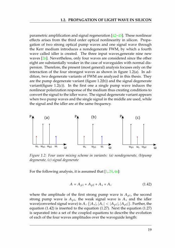
parametric amplification and signal regeneration [42–45]. These nonlineareffects arises from the third order optical nonlinearity in silicon. Propa-gation of two strong optical pump waves and one signal wave throughthe Kerr medium introduces a nondegenerate FWM, by which a fourthwave called idler is created. The three input waves,generate nine newwaves [26]. Nevertheless, only four waves are considered since the othereight are substantially weaker in the case of waveguides with normal dis-persion. Therefore, the present (most general) analysis focuses only on theinteraction of the four strongest waves as shown in figure 1.2(a). In ad-dition, two degenerate variants of FWM are analyzed in this thesis. Theyare the pump degenerate variant (figure 1.2(b)) and the signal degeneratevariant(figure 1.2(c)). In the first one a single pump wave induces thenonlinear polarization response of the medium thus creating conditions toconvert the signal to the idler wave. The signal degenerate variant appearswhen two pump waves and the single signal in the middle are used, whilethe signal and the idler are at the same frequency.
ωp1 ωp2ωs ωi ω
P (a) (c)(b)
ωp1ωs ωi ω
P
ω
P
ωp1 ωp2ωs
Figure 1.2: Four wave mixing scheme in variants: (a) nondegenerate, (b)pumpdegenerate, (c) signal degenerate
For the following analysis, it is assumed that [1, 29, 46]:
A = A p1 + A p2 + A s + A i (1.42)
where the amplitude of the first strong pump wave is A p1, the secondstrong pump wave is A p2, the weak signal wave is A s and the idlerwave(converted signal wave) is A i
(|A s |, |A i | < |A p1|, |A p2|
). Further, the
equation (1.42) is inserted to the equation (1.27). Next the equation (1.27)is separated into a set of the coupled equations to describe the evolutionof each of the four waves amplitudes over the waveguide length:
19
CHAPTER 1. BACKGROUND THEORY
∂A p1
∂z= − αlin
2A p1 + (iγp1 −
βTPA
2Aeff)
⎛⎝⏐⏐A p1⏐⏐2 + 2
∑m=p2,s ,i
|A m |2⎞⎠A p1+
+2iγp1A∗p2A s A i ei∆βz −
(ik0∆nFCD +
∆αFCA
2
)A p1
(1.43)
∂A p2
∂z= − αlin
2A p2 + (iγp2 −
βTPA
2Aeff)
⎛⎝|A p2|2 + 2∑
m=p1,s ,i
|A m |2⎞⎠A p2+
+2iγp2A∗p1A s A i e−i∆βz −
(ik0∆nFCD +
∆αFCA
2
)A p2
(1.44)
∂A s
∂z= − αlin
2A s + (iγs −
βTPA
2Aeff)
⎛⎝|A s |2 + 2∑
m=p1,p2,i
|A m |2⎞⎠A s +
+2iγs A p1A p2A∗i e−i∆βz −
(ik0∆nFCD +
∆αFCA
2
)A s
(1.45)
∂A i
∂z= − αlin
2A i + (iγi −
βTPA
2Aeff)
⎛⎝|A i |2 + 2∑
m=p1,p2,s
|A m |2⎞⎠A i +
+2iγi A p1A p2A∗s e−i∆βz −
(ik0∆nFCD +
∆αFCA
2
)A i
(1.46)
In the general case of the FWM process in a silicon waveguide, all thewaves contribute to the generation of the free carriers and thus to the in-crease of the loss coefficient ∆αFCA . However, the contribution of the weaksignal and the idler is neglected in the further calculations. The density ofthe free carriers generated by TPA process is then simplified to [36]:
Ne ,h =βTPA τeff
2hνAeff2 (P p1 + P p2)2 (1.47)
and allows to calculate ∆αFCA and ∆nFCD according to equations 1.29 and1.28 respectively. The physics of FWM can be explained by the condi-tions: the energy conservation and the momentum conservation (phase-matching condition) [47]. For the FWM described by the equations (1.43-1.46) these conditions can be expressed by the equations below:
20
1.2. PROPAGATION OF LIGHT WAVE IN SILICON
ωi = ωp1 + ωp2 − ωs (1.48)
∆β = βp1 + βp2 − βi − βs = 0 (1.49)
In section 3.3.6 the discussion will be limited to the pump degenerate ver-sion of FWM, where ωp1 = ωp2 = ωp , while the phase matching conditionand the energy conservation condition are simplified to:
∆β = 2βp − βi − βs = 0 (1.50)
∆ω = ωp − ωs = ωi − ωp (1.51)
ωi = 2ωp − ωs (1.52)
The SPM and XPM cause the nonlinear phase shift. In the case of the singlestrong pump this nonlinear phase shift must be taken into account andhaence the phase matching condition (1.50) changes into [27]:
∆knl = 2γPp −∆β (1.53)
where Pp is the power of the pump in the medium and the linear phasedifference is:
∆β = −β2(∆ω)2 − 112
β4(∆ω)4 (1.54)
where neff is the effective refractive index. Moreover, β2 and β4 are calcu-lated at the pump wavelength. Phase matching, required by momentumconservation in equation (1.53) can be provided by the waveguide disper-sion engineering. Silicon material dispersion needs compensation by theproper waveguide dimensions design to obtain the broadband operationand gain. As presented by Osgood et al. in [27], neglecting TPA, FCA andαlin , the formula for the conversion efficiency defined as a ratio betweenoutput idler power Pi (Lwg ) to input signal Ps (0) becomes:
η0L =Pi (Lwg )
Ps (0)=[γPp
gsinh (gLwg )
]2
, (1.55)
where
21
CHAPTER 1. BACKGROUND THEORY
g =
√γPp∆β −
(∆β
2
)2
(1.56)
represents the parametric gain and Lwg is the length of interaction in thisideal case. If ∆β = 2γPp then equation (1.55) is reduced to:
η0L ,max = sinh2 (γP p Lwg ). (1.57)
In [27, 48] authors used the definition of wavelength conversion band-width when |∆k nl Lwg | < π. Under the assumption of the small gain limitwhen 2γPp Lwg ≪ π, the wavelength conversion bandwidth can be ex-pressed as:
BWFWM ≈
√4π
β2Lwg(1.58)
where β2 is the group velocity dispersion coefficient. These formulas givea good estimation of the maximum possible FWM wavelength conversionefficiency in the silicon waveguide.
1.2.9 Four wave mixing simulation model
The four wave mixing in the silicon waveguide is approximated by thefirst order nonlinear Schrodinger equation (described in section 1.2.3). Itprovids a good agreement to the measurement results available in the lit-erature [27, 28, 42, 43]. For the FWM simulations, the model introducedby Jazayerifar and Dziallas et al. in [28, 46] is used. The method matcheswell with other models developed by the research groups working in thefield [27, 49–51]. The nonlinear Schrodinger equation (NLSE) (equation(1.27)) with the sum amplitude from the equation (1.42) is solved numeri-cally using the Fourier split step method [1, 26, 28]. This methods relies onthe assumption that the linear and nonlinear effects can be treated sep-arately, if sufficiently small propagation distance is taken into account.Therefore, dividing the waveguide in small segments of the length ∆z ,the amplitude evolution can be approximated by:
22
1.2. PROPAGATION OF LIGHT WAVE IN SILICON
A (z + ∆z , t ) = A (z , t )(
e12 ∆zD e∆zN e
12 ∆zD
)(1.59)
where the differential operators are defined by:
D = −iβ2
2∂2
∂t 2 − αlin
2(1.60)
N = −iγ|A |2 − βTPA
2Aeff|A |2 − ik0∆nFCD − ∆αFCA
2(1.61)
where β2 is a group velocity dispersion defined in equation (1.22), αlin islinear loss coefficient of the waveguide. The γ is nonlinear coefficient de-fined as in equation (1.25), βTPA is TPA coefficient introduced in equation(1.11). The terms ∆αFCA and ∆nFCD were calculated with the formulas(1.31) and (1.33). The numerical simulations were performed in the Mat-lab environment. The steps using Fast Fourier Transform (fft) and InverseFast Fourier Transform (ifft) within one ∆z step were realized in the fol-lowing order [28]:
A(
z +12∆z , t
)= ifft
{fft (A (z , t )) · e
(i β2
2 ω2− 12 αlin
)· 1
2 ∆z}
(1.62)
A(
z +12∆z , t
)= A (z +
12∆z , t ) · e(−iγ|A |2− 1
2 αTPA −ik0∆nFCD − 12 ∆αFCA ) (1.63)
A (z + ∆z , t ) = ifft{
fft(
A (z +12∆z , t )
)·(
e(
i β22 ω2− 1
2 αlin
)· 1
2 ∆z)}
(1.64)
where the ω is a vector consisting of all the frequencies taken into accountfor the nonlinear propagation simulations.
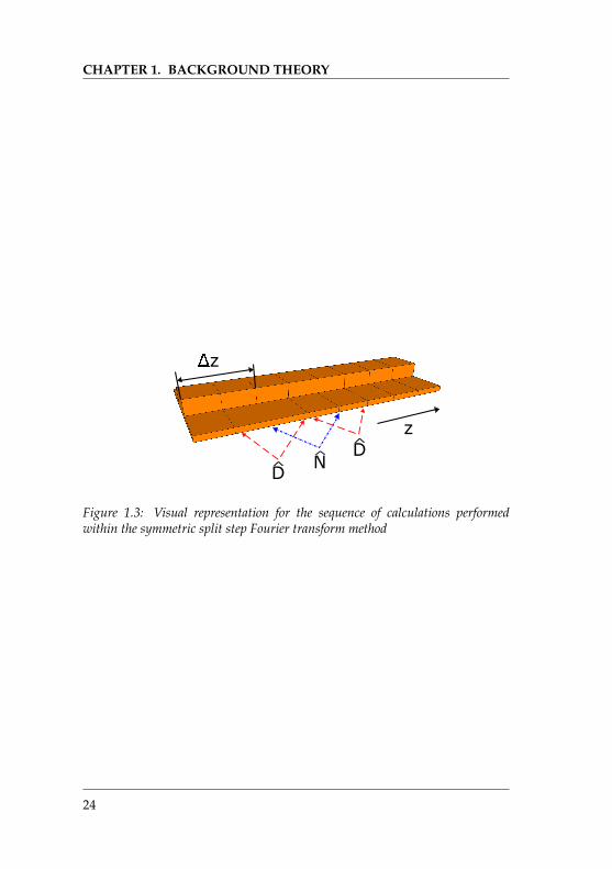
The graphical interpretation of the implementation of the symetric splitstep Fourier method is presented in figure 1.3. The symmetric split stepFourier transform method was used to design structures as well as forbetter understanding of the obtained measurement results and finally tooptimize waveguide structures.
23
CHAPTER 1. BACKGROUND THEORY
D^ N
^
z
z
D^
Figure 1.3: Visual representation for the sequence of calculations performedwithin the symmetric split step Fourier transform method
24
2Numerical simulations of the SOI waveguide
for CW four wave mixing
Designing samples for the nonlinear interaction will be presented in thischapter including different aspects of the structures optimization. Thischapter contains detailed information about the models, parameters andproperties of the materials used in the design process. It will start withthe optical properties of the applied materials, which were necessary forthe sample fabrication. Each property will be explained using an appro-priate model. Then the linear optical properties of the waveguide such asa linear loss and dispersion shall be introduced. The further analysis willcontain placing doped regions aside the waveguide and its consequencefor the waveguide loss. Later results of the power dependent loss simu-lations will be presented. Moreover, the possibility of increasing recombi-nation rate e.g. shortening the effective free carriers lifetime (τeff ) will beanalyzed.
2.1 Optical properties approximation of applied materials
2.1.1 Linear absorption of bulk Si
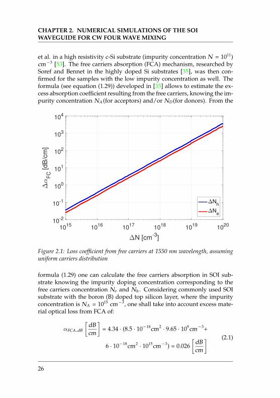
The key material feature, as regards the propagation of an optical signal iscertainly the linear absorption (known as well as a single-photon absorp-tion [2]). The linear optical loss of c-Si has been expected to be low for theoptical wavelengths longer then 1200 nm due to its relatively high, indi-rect energy gap Eg = 1.12 eV [35, 52]. Indeed in 2013 optical absorption aslow as 2 · 10−5 dB/cm was measured at 1550 nm wavelength by Degallaix
25
CHAPTER 2. NUMERICAL SIMULATIONS OF THE SOIWAVEGUIDE FOR CW FOUR WAVE MIXING
et al. in a high resistivity c-Si substrate (impurity concentration N = 1011)cm−3 [53]. The free carriers absorption (FCA) mechanism, researched bySoref and Bennet in the highly doped Si substrates [35], was then con-firmed for the samples with the low impurity concentration as well. Theformula (see equation (1.29)) developed in [35] allows to estimate the ex-cess absorption coefficient resulting from the free carriers, knowing the im-purity concentration NA (for acceptors) and/or ND (for donors). From the
1015
1016
1017
1018
1019
1020
N [cm-3
]
10-2
10-1
100
101
102
103
104
FC
[dB
/cm
]
Nh
Ne
Figure 2.1: Loss coefficient from free carriers at 1550 nm wavelength, assuminguniform carriers distribution
formula (1.29) one can calculate the free carriers absorption in SOI sub-strate knowing the impurity doping concentration corresponding to thefree carriers concentration Ne and Nh . Considering commonly used SOIsubstrate with the boron (B) doped top silicon layer, where the impurityconcentration is NA = 1015 cm−3, one shall take into account excess mate-rial optical loss from FCA of:
αFCA dB
[dBcm
]= 4.34 · (8.5 · 10−18cm2 · 9.65 · 109cm−3+
6 · 10−18cm2 · 1015cm−3) = 0.026[
dBcm
] (2.1)
26
2.1. OPTICAL PROPERTIES APPROXIMATION OF APPLIEDMATERIALS
This shows that the pure silicon loss is about three orders of magnitudelower than the excess loss introduced by the impurity. Figure 2.1 depictsthe relation between the carrier concentration (impurity concentration)and the excess loss. The results obtained in this short analysis and citedreferences suggest, that the major fraction of the optical loss in bulk Si canbe attributed to the free carriers coming from impurities.
2.1.2 Two photon absorption and free carriers absorption in-duced by two-photon absorption
Exposing silicon Si to the high intensity light with hc/Eg < λ < hc/Eg
enables an effect known as two photon absorption TPA. Two photons, thatin sum have energy higher then Eg , are absorbed simultaneously by thesemiconductor material and create a free electron-hole pair. This effectis orders of magnitude weaker then the linear absorption and thereforebecomes pronounced for the high light intensities ( e.g. in Si over 0.1 · 109
W/cm2 at λ = 1550nm). The loss due to TPA and TPA induced FCA wascalculated from the corresponding formulas defined in the section 1.2.4.The value of βTPA = 0.56 ·10−9cm/W was obtained from the measurementreported later in the thesis in section 3.3.5.
2.1.3 Material dispersion of silicon, silicon nitride and siliconoxide
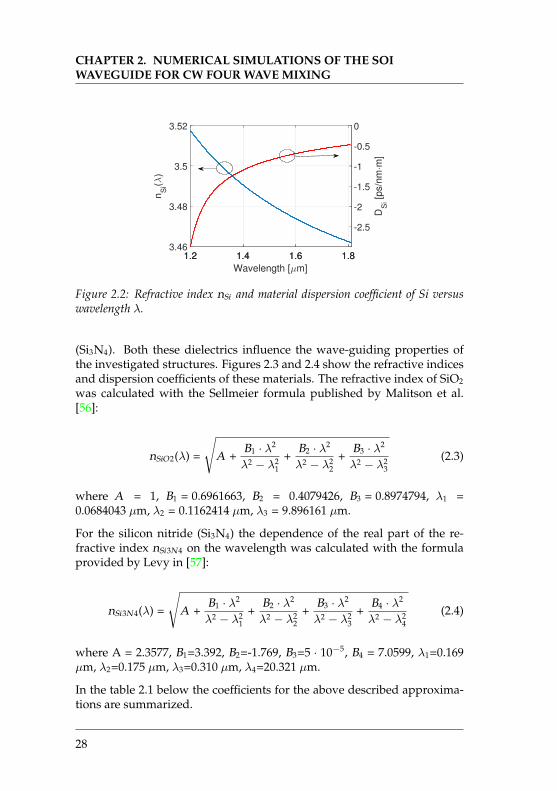
Simulation of the integrated, silicon based photonic structures requirestaking into account dispersion of silicon and surrounding materials. In thefollowing numerical calculations, we use the relation of the real part of therefractive index of Si versus wavelength λ given by the equation [27, 54]:
nSi (λ) =
√A +
B1
λ2 +B2 · λ2
λ2 − λ21
(2.2)
where A = εSi (λ → ∞) = 11.6858, λ1 = 1.1071 µm, B1 = 0.939816 µm2,B2 = 8.10461 · 10−3. The blue curve in figure 2.2 shows this relation, whilethe red one depicts the chromatic dispersion coefficient (D ) according tothe formula (1.23) [55]:
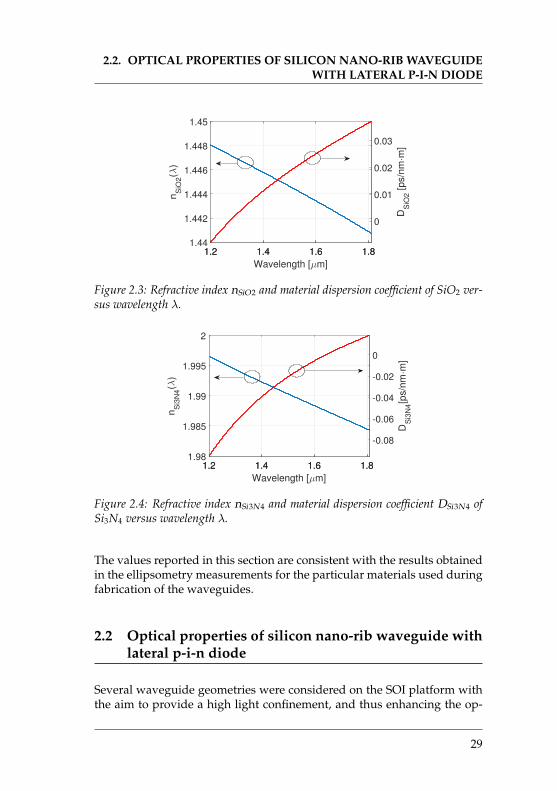
Two other materials, used in the available technology for fabrication of thephotonic integrated structures were silicon oxide (SiO2) and silicon nitride
27
CHAPTER 2. NUMERICAL SIMULATIONS OF THE SOIWAVEGUIDE FOR CW FOUR WAVE MIXING
Wavelength [µm]
1.2 1.4 1.6 1.8
nS
i(λ)
3.46
3.48
3.5
3.52
1.2 1.4 1.6 1.8
DS
i [ps/n
m·m
]
-2.5
-2
-1.5
-1
-0.5
0
Figure 2.2: Refractive index nSi and material dispersion coefficient of Si versuswavelength λ.
(Si3N4). Both these dielectrics influence the wave-guiding properties ofthe investigated structures. Figures 2.3 and 2.4 show the refractive indicesand dispersion coefficients of these materials. The refractive index of SiO2
was calculated with the Sellmeier formula published by Malitson et al.[56]:
nSiO2(λ) =
√A +
B1 · λ2
λ2 − λ21
+B2 · λ2
λ2 − λ22
+B3 · λ2
λ2 − λ23
(2.3)
where A = 1, B1 = 0.6961663, B2 = 0.4079426, B3 = 0.8974794, λ1 =0.0684043 µm, λ2 = 0.1162414 µm, λ3 = 9.896161 µm.
For the silicon nitride (Si3N4) the dependence of the real part of the re-fractive index nSi3N4 on the wavelength was calculated with the formulaprovided by Levy in [57]:
nSi3N4(λ) =
√A +
B1 · λ2
λ2 − λ21
+B2 · λ2
λ2 − λ22
+B3 · λ2
λ2 − λ23
+B4 · λ2
λ2 − λ24
(2.4)
where A = 2.3577, B1=3.392, B2=-1.769, B3=5 · 10−5, B4 = 7.0599, λ1=0.169µm, λ2=0.175 µm, λ3=0.310 µm, λ4=20.321 µm.
In the table 2.1 below the coefficients for the above described approxima-tions are summarized.
28
2.2. OPTICAL PROPERTIES OF SILICON NANO-RIB WAVEGUIDEWITH LATERAL P-I-N DIODE
Wavelength [µm]
1.2 1.4 1.6 1.8
nS
iO2(λ
)
1.44
1.442
1.444
1.446
1.448
1.45
1.2 1.4 1.6 1.8
DS
iO2 [ps/n
m·m
]
0
0.01
0.02
0.03
Figure 2.3: Refractive index nSiO2 and material dispersion coefficient of SiO2 ver-sus wavelength λ.
Wavelength [µm]
1.2 1.4 1.6 1.8
nS
i3N
4(λ
)
1.98
1.985
1.99
1.995
2
1.2 1.4 1.6 1.8
DS
i3N
4[p
s/n
m·m
]
-0.08
-0.06
-0.04
-0.02
0
Figure 2.4: Refractive index nSi3N4 and material dispersion coefficient DSi3N4 ofSi3N4 versus wavelength λ.
The values reported in this section are consistent with the results obtainedin the ellipsometry measurements for the particular materials used duringfabrication of the waveguides.
2.2 Optical properties of silicon nano-rib waveguide withlateral p-i-n diode
Several waveguide geometries were considered on the SOI platform withthe aim to provide a high light confinement, and thus enhancing the op-
29
CHAPTER 2. NUMERICAL SIMULATIONS OF THE SOIWAVEGUIDE FOR CW FOUR WAVE MIXING
ModelCoefficient Si [27, 54] SiO2 [56] Si3N4 [57]
A 11.6858 1 2.3577B1 0.939816 µm2 0.6961663 3.392B2 8.10461 · 10−3 0.4079426 -1.769B3 - 0.8974794 5 · 10−5
B4 - - 7.0599λ1 1.1071 µm 0.0684043 µm 0.169 µmλ2 - 0.1162414 µm 0.175 µmλ3 - 9.896161 µm 0.310µmλ4 - - 20.321µm
Table 2.1: Coefficients used in the approximation of the materials’ dispersion
tical Kerr effect [27, 33, 42, 43, 48, 58, 59]. Therefore, a sub-micron dimen-sion stripe of silicon surrounded by low refractive index material like airor SiO2 was used to guide the light to analyze the nonlinear optical ef-fects [48, 60]. These experiments showed the detrimental influence of TPAand TPA induced FCA, apart from the enhancement in the nonlinear coef-ficient γ. To overcome the limitation due to the FCA the free carrier den-sity in the wave-guiding area shall be suppressed. In order to fulfill therequirements of small Aeff and the low free carriers density it was decidedto produce the sub-micron size nano-rib waveguide assisted by the lateralp-i-n diode [58].
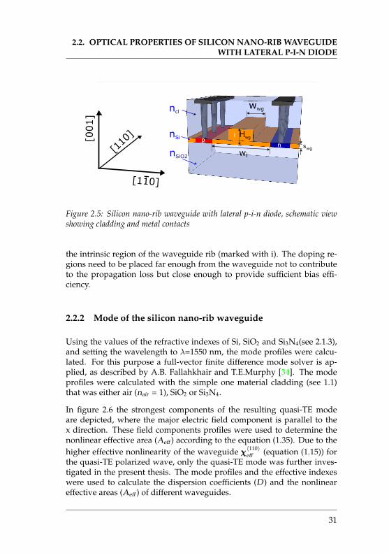
2.2.1 Structure of the modeled waveguide
The commonly used SOI wafer consists of a silicon substrate with SiO2
with a few micrometers thickness (typically from 1 to 3 µm) and a Si layeron the top (typically 220 nm thick). The waveguide is created by formingof a stripe pattern in the top silicon layer. Later it can be covered by an-other material. The considered structures were covered with both SiO2 andSi3N4. Before the final choice of the dimensions of the waveguide for fab-rication with a lateral p-i-n diode, different variants of a sub-micrometersingle mode silicon rib waveguide were investigated.
Figure 2.5 depicts the general scheme of the waveguide considered for theevaluation. Next to the waveguide p- and n-doped regions were created.They provide connection of the bias voltage to induce an electric field in
30
2.2. OPTICAL PROPERTIES OF SILICON NANO-RIB WAVEGUIDEWITH LATERAL P-I-N DIODE
wwg
Hwg
nSiO2
nSi
ncl
wiwg
[001]
[110]
[110]-
Figure 2.5: Silicon nano-rib waveguide with lateral p-i-n diode, schematic viewshowing cladding and metal contacts
the intrinsic region of the waveguide rib (marked with i). The doping re-gions need to be placed far enough from the waveguide not to contributeto the propagation loss but close enough to provide sufficient bias effi-ciency.
2.2.2 Mode of the silicon nano-rib waveguide
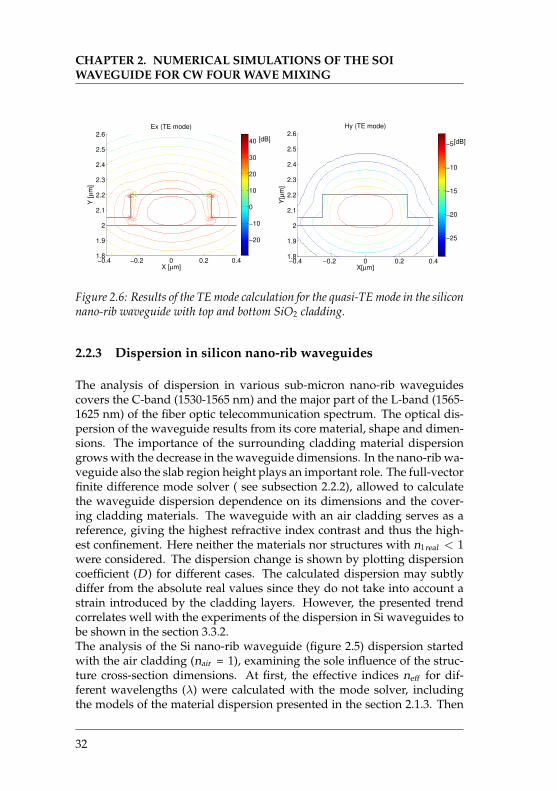
Using the values of the refractive indexes of Si, SiO2 and Si3N4(see 2.1.3),and setting the wavelength to λ=1550 nm, the mode profiles were calcu-lated. For this purpose a full-vector finite difference mode solver is ap-plied, as described by A.B. Fallahkhair and T.E.Murphy [34]. The modeprofiles were calculated with the simple one material cladding (see 1.1)that was either air (nair = 1), SiO2 or Si3N4.
In figure 2.6 the strongest components of the resulting quasi-TE modeare depicted, where the major electric field component is parallel to thex direction. These field components profiles were used to determine thenonlinear effective area (Aeff ) according to the equation (1.35). Due to thehigher effective nonlinearity of the waveguide χχχ
⟨110⟩eff (equation (1.15)) for
the quasi-TE polarized wave, only the quasi-TE mode was further inves-tigated in the present thesis. The mode profiles and the effective indexeswere used to calculate the dispersion coefficients (D ) and the nonlineareffective areas (Aeff ) of different waveguides.
31
CHAPTER 2. NUMERICAL SIMULATIONS OF THE SOIWAVEGUIDE FOR CW FOUR WAVE MIXING
−0.4 −0.2 0 0.2 0.41.8
1.9
2
2.1
2.2
2.3
2.4
2.5
2.6Hy (TE mode)
Y[µ
m]
X[µm]−0.4 −0.2 0 0.2 0.41.8
1.9
2
2.1
2.2
2.3
2.4
2.5
2.6Ex (TE mode)
X [µm]
Y [
µm
]
−20
−10
0
10
20
30
40
−25
−20
−15
−10
−5[dB][dB]
Figure 2.6: Results of the TE mode calculation for the quasi-TE mode in the siliconnano-rib waveguide with top and bottom SiO2 cladding.
2.2.3 Dispersion in silicon nano-rib waveguides
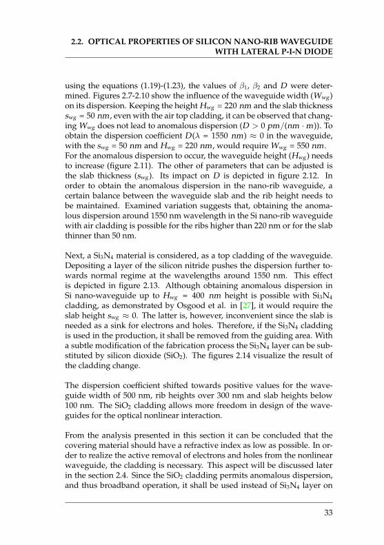
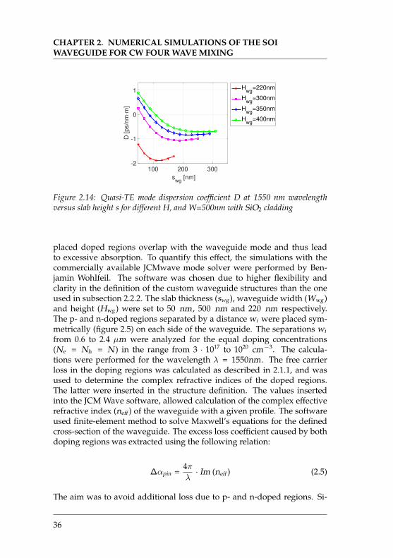
The analysis of dispersion in various sub-micron nano-rib waveguidescovers the C-band (1530-1565 nm) and the major part of the L-band (1565-1625 nm) of the fiber optic telecommunication spectrum. The optical dis-persion of the waveguide results from its core material, shape and dimen-sions. The importance of the surrounding cladding material dispersiongrows with the decrease in the waveguide dimensions. In the nano-rib wa-veguide also the slab region height plays an important role. The full-vectorfinite difference mode solver ( see subsection 2.2.2), allowed to calculatethe waveguide dispersion dependence on its dimensions and the cover-ing cladding materials. The waveguide with an air cladding serves as areference, giving the highest refractive index contrast and thus the high-est confinement. Here neither the materials nor structures with n1real < 1were considered. The dispersion change is shown by plotting dispersioncoefficient (D ) for different cases. The calculated dispersion may subtlydiffer from the absolute real values since they do not take into account astrain introduced by the cladding layers. However, the presented trendcorrelates well with the experiments of the dispersion in Si waveguides tobe shown in the section 3.3.2.The analysis of the Si nano-rib waveguide (figure 2.5) dispersion startedwith the air cladding (nair = 1), examining the sole influence of the struc-ture cross-section dimensions. At first, the effective indices neff for dif-ferent wavelengths (λ) were calculated with the mode solver, includingthe models of the material dispersion presented in the section 2.1.3. Then
32
2.2. OPTICAL PROPERTIES OF SILICON NANO-RIB WAVEGUIDEWITH LATERAL P-I-N DIODE
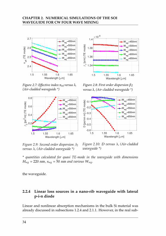
using the equations (1.19)-(1.23), the values of β1, β2 and D were deter-mined. Figures 2.7-2.10 show the influence of the waveguide width (Wwg )on its dispersion. Keeping the height Hwg = 220 nm and the slab thicknessswg = 50 nm , even with the air top cladding, it can be observed that chang-ing Wwg does not lead to anomalous dispersion (D > 0 pm/(nm · m)). Toobtain the dispersion coefficient D (λ = 1550 nm) ≈ 0 in the waveguide,with the swg = 50 nm and Hwg = 220 nm , would require Wwg = 550 nm .For the anomalous dispersion to occur, the waveguide height (Hwg ) needsto increase (figure 2.11). The other of parameters that can be adjusted isthe slab thickness (swg ). Its impact on D is depicted in figure 2.12. Inorder to obtain the anomalous dispersion in the nano-rib waveguide, acertain balance between the waveguide slab and the rib height needs tobe maintained. Examined variation suggests that, obtaining the anoma-lous dispersion around 1550 nm wavelength in the Si nano-rib waveguidewith air cladding is possible for the ribs higher than 220 nm or for the slabthinner than 50 nm.
Next, a Si3N4 material is considered, as a top cladding of the waveguide.Depositing a layer of the silicon nitride pushes the dispersion further to-wards normal regime at the wavelengths around 1550 nm. This effectis depicted in figure 2.13. Although obtaining anomalous dispersion inSi nano-waveguide up to Hwg = 400 nm height is possible with Si3N4
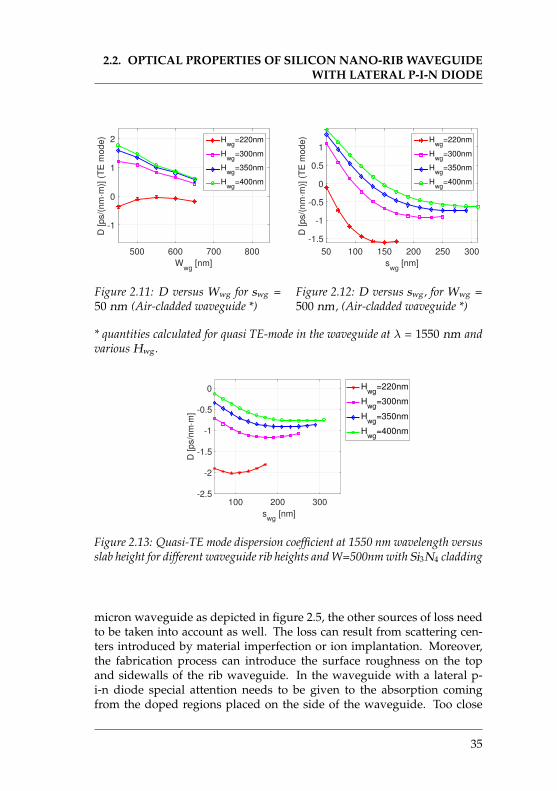
cladding, as demonstrated by Osgood et al. in [27], it would require theslab height swg ≈ 0. The latter is, however, inconvenient since the slab isneeded as a sink for electrons and holes. Therefore, if the Si3N4 claddingis used in the production, it shall be removed from the guiding area. Witha subtle modification of the fabrication process the Si3N4 layer can be sub-stituted by silicon dioxide (SiO2). The figures 2.14 visualize the result ofthe cladding change.
The dispersion coefficient shifted towards positive values for the wave-guide width of 500 nm, rib heights over 300 nm and slab heights below100 nm. The SiO2 cladding allows more freedom in design of the wave-guides for the optical nonlinear interaction.
From the analysis presented in this section it can be concluded that thecovering material should have a refractive index as low as possible. In or-der to realize the active removal of electrons and holes from the nonlinearwaveguide, the cladding is necessary. This aspect will be discussed laterin the section 2.4. Since the SiO2 cladding permits anomalous dispersion,and thus broadband operation, it shall be used instead of Si3N4 layer on
33
CHAPTER 2. NUMERICAL SIMULATIONS OF THE SOIWAVEGUIDE FOR CW FOUR WAVE MIXING
Wavelength [µm]
1.5 1.55 1.6 1.65
neff (
TE
mo
de
)
2.4
2.5
2.6
2.7W
wg=450nm
Wwg
=500nm
Wwg
=550nm
Wwg
=600nm
Wwg
=650nm
Wavelength [µm]
1.5 1.55 1.6 1.65
β1 [
s/m
] (T
E m
od
e)
×10-8
1.34
1.36
1.38
1.4W
wg=450nm
Wwg
=500nm
Wwg
=550nm
Wwg
=600nm
Wwg
=650nm
Figure 2.8: First order dispersion β1versus λ, (Air-cladded waveguide *)
Wavelength [µm]
1.5 1.55 1.6 1.65
β2 [
ps
2/m
] (T
E m
od
e)
0.2
0.4
0.6
0.8W
wg=450nm
Wwg
=500nm
Wwg
=550nm
Wwg
=600nm
Wwg
=650nm
Figure 2.9: Second order dispersion β2
versus λ, (Air-cladded waveguide *)
Wavelength [µm]
1.5 1.55 1.6 1.65
D [
ps/n
m·m
] (T
E m
od
e)
-0.6
-0.5
-0.4
-0.3
-0.2
-0.1W
wg=450nm
Wwg
=500nm
Wwg
=550nm
Wwg
=600nm
Wwg
=650nm
Figure 2.10: D versus λ, (Air-claddedwaveguide *)
* quantities calculated for quasi TE-mode in the waveguide with dimensionsHwg = 220 nm , swg = 50 nm and various Wwg .
the waveguide.
2.2.4 Linear loss sources in a nano-rib waveguide with lateralp-i-n diode
Linear and nonlinear absorption mechanisms in the bulk Si material wasalready discussed in subsections 1.2.4 and 2.1.1. However, in the real sub-
34
Figure 2.7: Effective index neff versus λ, (Air-cladded waveguide *)
2.2. OPTICAL PROPERTIES OF SILICON NANO-RIB WAVEGUIDEWITH LATERAL P-I-N DIODE
Wwg
[nm]
500 600 700 800
D [
ps/(
nm·m
)] (
TE
mo
de
)
-1
0
1
2 Hwg
=220nm
Hwg
=300nm
Hwg
=350nm
Hwg
=400nm
Figure 2.11: D versus Wwg for swg =50 nm (Air-cladded waveguide *)
swg
[nm]
50 100 150 200 250 300
D [
ps/(
nm·m
)] (
TE
mo
de
)
-1.5
-1
-0.5
0
0.5
1H
wg=220nm
Hwg
=300nm
Hwg
=350nm
Hwg
=400nm
Figure 2.12: D versus swg , for Wwg =500 nm , (Air-cladded waveguide *)
* quantities calculated for quasi TE-mode in the waveguide at λ = 1550 nm andvarious Hwg .
100 200 300
swg
[nm]
-2.5
-2
-1.5
-1
-0.5
0
D [ps/n
mm
]
Hwg
=220nm
Hwg
=300nm
Hwg
=350nm
Hwg
=400nm
Figure 2.13: Quasi-TE mode dispersion coefficient at 1550 nm wavelength versusslab height for different waveguide rib heights and W=500nm with Si3N4 cladding
micron waveguide as depicted in figure 2.5, the other sources of loss needto be taken into account as well. The loss can result from scattering cen-ters introduced by material imperfection or ion implantation. Moreover,the fabrication process can introduce the surface roughness on the topand sidewalls of the rib waveguide. In the waveguide with a lateral p-i-n diode special attention needs to be given to the absorption comingfrom the doped regions placed on the side of the waveguide. Too close
35
CHAPTER 2. NUMERICAL SIMULATIONS OF THE SOIWAVEGUIDE FOR CW FOUR WAVE MIXING
100 200 300
swg
[nm]
-2
-1
0
1
D [ps/n
mm
]
Hwg
=220nm
Hwg
=300nm
Hwg
=350nm
Hwg
=400nm
Figure 2.14: Quasi-TE mode dispersion coefficient D at 1550 nm wavelengthversus slab height s for different H, and W=500nm with SiO2 cladding
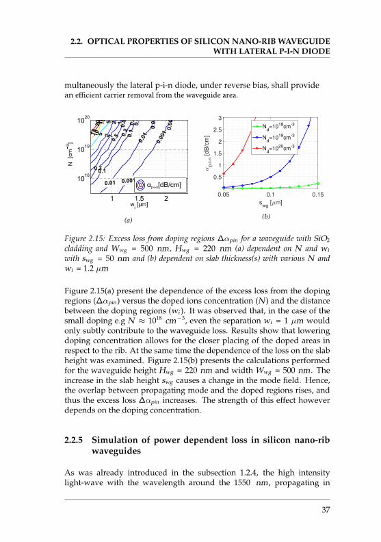
placed doped regions overlap with the waveguide mode and thus leadto excessive absorption. To quantify this effect, the simulations with thecommercially available JCMwave mode solver were performed by Ben-jamin Wohlfeil. The software was chosen due to higher flexibility andclarity in the definition of the custom waveguide structures than the oneused in subsection 2.2.2. The slab thickness (swg ), waveguide width (Wwg )and height (Hwg ) were set to 50 nm , 500 nm and 220 nm respectively.The p- and n-doped regions separated by a distance wi were placed sym-metrically (figure 2.5) on each side of the waveguide. The separations wi
from 0.6 to 2.4 µm were analyzed for the equal doping concentrations(Ne = Nh = N ) in the range from 3 · 1017 to 1020 cm−3. The calcula-tions were performed for the wavelength λ = 1550nm . The free carrierloss in the doping regions was calculated as described in 2.1.1, and wasused to determine the complex refractive indices of the doped regions.The latter were inserted in the structure definition. The values insertedinto the JCM Wave software, allowed calculation of the complex effectiverefractive index (neff ) of the waveguide with a given profile. The softwareused finite-element method to solve Maxwell’s equations for the definedcross-section of the waveguide. The excess loss coefficient caused by bothdoping regions was extracted using the following relation:
∆αpin =4πλ
· Im (neff ) (2.5)
The aim was to avoid additional loss due to p- and n-doped regions. Si-
36
2.2. OPTICAL PROPERTIES OF SILICON NANO-RIB WAVEGUIDEWITH LATERAL P-I-N DIODE
multaneously the lateral p-i-n diode, under reverse bias, shall provide an efficient carrier removal from the waveguide area.
0.001
0.001
0.001
0.01
0.01
0.01
0.1
0.1
0.1
0.2
0.2
0.2
0.5
0.5
1
12
25
510
10
15
1520
wi[µm]
N[c
m3]
1 1.5 2
1018
1019
1020
αp-i-n[dB/cm]
(a)
swg
[µm]
0.05 0.1 0.15
αp
-i-n
[d
B/c
m]
0.5
1
1.5
2
2.5
3
Nd=10
18cm
-3
Nd=10
19cm
-3
Nd=10
20cm
-3
(b)
Figure 2.15: Excess loss from doping regions ∆αpin for a waveguide with SiO2
cladding and Wwg = 500 nm , Hwg = 220 nm (a) dependent on N and wi
with swg = 50 nm and (b) dependent on slab thickness(s) with various N andwi = 1.2 µm
Figure 2.15(a) present the dependence of the excess loss from the dopingregions (∆αpin ) versus the doped ions concentration (N ) and the distancebetween the doping regions (wi ). It was observed that, in the case of thesmall doping e.g N ≈ 1018 cm−3, even the separation wi = 1 µm wouldonly subtly contribute to the waveguide loss. Results show that loweringdoping concentration allows for the closer placing of the doped areas inrespect to the rib. At the same time the dependence of the loss on the slabheight was examined. Figure 2.15(b) presents the calculations performedfor the waveguide height Hwg = 220 nm and width Wwg = 500 nm . Theincrease in the slab height swg causes a change in the mode field. Hence,the overlap between propagating mode and the doped regions rises, andthus the excess loss ∆αpin increases. The strength of this effect howeverdepends on the doping concentration.
2.2.5 Simulation of power dependent loss in silicon nano-ribwaveguides
As was already introduced in the subsection 1.2.4, the high intensitylight-wave with the wavelength around the 1550 nm , propagating in
37
CHAPTER 2. NUMERICAL SIMULATIONS OF THE SOIWAVEGUIDE FOR CW FOUR WAVE MIXING
a silicon waveguide, induces the free carriers generation via TPA phe-nomenon. The average density of free carriers in the waveguide cross-section can be calculated then with the equation (1.30) [29]. The changein the optical power P along the waveguide propagation direction z , dueto TPA and TPA induced FCA can be described using the following for-mula [29]:
dP (z)dz
= −αlin · P (z) − βTPA
Aeff· P 2(z) −∆αFCA P (z) (2.6)
where αlin is the linear loss coefficient, βTPA is the TPA coefficient, ∆αFCA
is expressed as in equation (1.31).
Numerical calculations were performed to investigate the sole influenceof linear loss, TPA and TPA induced FCA. The calculations considered thewaveguide height Hwg = 220 nm , width Wwg = 500 nm and slab thicknessswg = 50 nm
(Aeff = 0.1 µm2). The TPA coefficient βTPA was assumed to
be 5.6 · 10−10cm/W in all the calculations. The value of βTPA is the resultof the measurement referred to in subsection 3.3.5). The calculations wereperformed applying the method introduced in subsection 1.2.9, consider-ing the single wave propagating through the waveguide with the inputpower P (0).
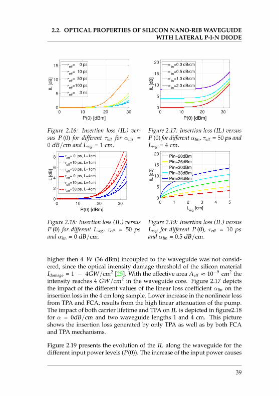
Here the total insertion loss of the waveguide is defined as:
IL [dB ] = 10 · log10
(P (0)
P(Lwg
)) (2.7)
were the optical power P is given in Watts. At first (figure 2.16), the im-pact of TPA (τeff = 0ps , blue curve) on IL was investigated. Then TPAinduced FCA with τeff up to 3 ns was examined as a function of the inputpower (P (0)). The free carrier lifetime τeff , as short as 50 ps with the in-put power P (0) = 30 dBm causes substantial loss increase. At this inputpower the 3 ns free carrier lifetime results for this power in over 10 dBexcess loss. The τeff of 3 ns is commonly assumed for the case of the sub-micron silicon waveguides without a lateral p-i-n diode. The high TPAinduced FCA could have been a reason to consider different material plat-forms or a pulsed operation with the low repetition rate to benefit fromnonlinear optical effects.Secondly the impact of the linear loss on IL was examined. Here the power
38
2.2. OPTICAL PROPERTIES OF SILICON NANO-RIB WAVEGUIDEWITH LATERAL P-I-N DIODE
P(0) [dBm]
0 10 20 30
IL [
dB
]
0
5
10
15 τeff
= 0 ps
τeff
= 10 ps
τeff
= 50 ps
τeff
=100 ps
τeff
= 3 ns
Figure 2.16: Insertion loss (IL ) ver-sus P (0) for different τeff for αlin =0 dB/cm and Lwg = 1 cm .
P(0) [dBm]
0 10 20 30
IL [
dB
]
0
5
10
15
20α
lin=0.0 dB/cm
αlin
=0.5 dB/cm
αlin
=1.0 dB/cm
αlin
=2.0 dB/cm
Figure 2.17: Insertion loss (IL ) versusP (0) for different αlin , τeff = 50 ps andLwg = 4 cm .
P(0) [dBm]
0 10 20 30
IL [
dB
]
0
2
4
6
8 τeff
= 0 ps, L=1cm
τeff
=10 ps, L=1cm
τeff
=50 ps, L=1cm
τeff
= 0 ps, L=4cm
τeff
=10 ps, L=4cm
τeff
=50 ps, L=4cm
Figure 2.18: Insertion loss (IL ) versusP (0) for different Lwg , τeff = 50 psand αlin = 0 dB/cm .
Lwg
[cm]
0 1 2 3 4 5
IL [
dB
]
0
5
10
15
20 Pin=20dBm
Pin=26dBm
Pin=30dBm
Pin=33dBm
Pin=36dBm
Figure 2.19: Insertion loss (IL ) versusLwg for different P (0), τeff = 10 psand αlin = 0.5 dB/cm .
higher then 4 W (36 dBm) incoupled to the waveguide was not consid-ered, since the optical intensity damage threshold of the silicon materialIdamage = 1 − 4GW/cm2 [25]. With the effective area Aeff ≈ 10−9 cm2 theintensity reaches 4 GW/cm2 in the waveguide core. Figure 2.17 depictsthe impact of the different values of the linear loss coefficient αlin on theinsertion loss in the 4 cm long sample. Lower increase in the nonlinear lossfrom TPA and FCA, results from the high linear attenuation of the pump.The impact of both carrier lifetime and TPA on IL is depicted in figure2.18for α = 0dB/cm and two waveguide lengths 1 and 4 cm. This pictureshows the insertion loss generated by only TPA as well as by both FCAand TPA mechanisms.
Figure 2.19 presents the evolution of the IL along the waveguide for thedifferent input power levels (P (0)). The increase of the input power causes
39
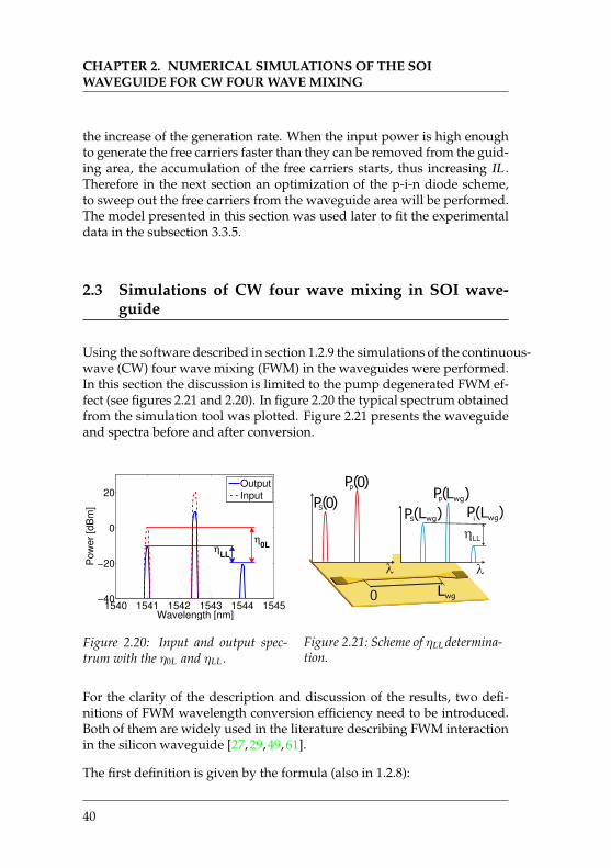
CHAPTER 2. NUMERICAL SIMULATIONS OF THE SOIWAVEGUIDE FOR CW FOUR WAVE MIXING
the increase of the generation rate. When the input power is high enoughto generate the free carriers faster than they can be removed from the guid-ing area, the accumulation of the free carriers starts, thus increasing IL .Therefore in the next section an optimization of the p-i-n diode scheme,to sweep out the free carriers from the waveguide area will be performed.The model presented in this section was used later to fit the experimentaldata in the subsection 3.3.5.
2.3 Simulations of CW four wave mixing in SOI wave-guide
Using the software described in section 1.2.9 the simulations of the continuous-wave (CW) four wave mixing (FWM) in the waveguides were performed.In this section the discussion is limited to the pump degenerated FWM ef-fect (see figures 2.21 and 2.20). In figure 2.20 the typical spectrum obtainedfrom the simulation tool was plotted. Figure 2.21 presents the waveguideand spectra before and after conversion.
1540 1541 1542 1543 1544 1545−40
−20
0
20
Wavelength [nm]
Pow
er
[dB
m]
OutputInput
η0L
ηLL
Figure 2.20: Input and output spec-trum with the η0L and ηLL .
Pp )(0
LwgPi
Lwg
)(LwgPS )()0PS(
Pp(Lwg)
Figure 2.21: Scheme of ηLL determina-tion.
For the clarity of the description and discussion of the results, two defi-nitions of FWM wavelength conversion efficiency need to be introduced.Both of them are widely used in the literature describing FWM interactionin the silicon waveguide [27, 29, 49, 61].
The first definition is given by the formula (also in 1.2.8):
40
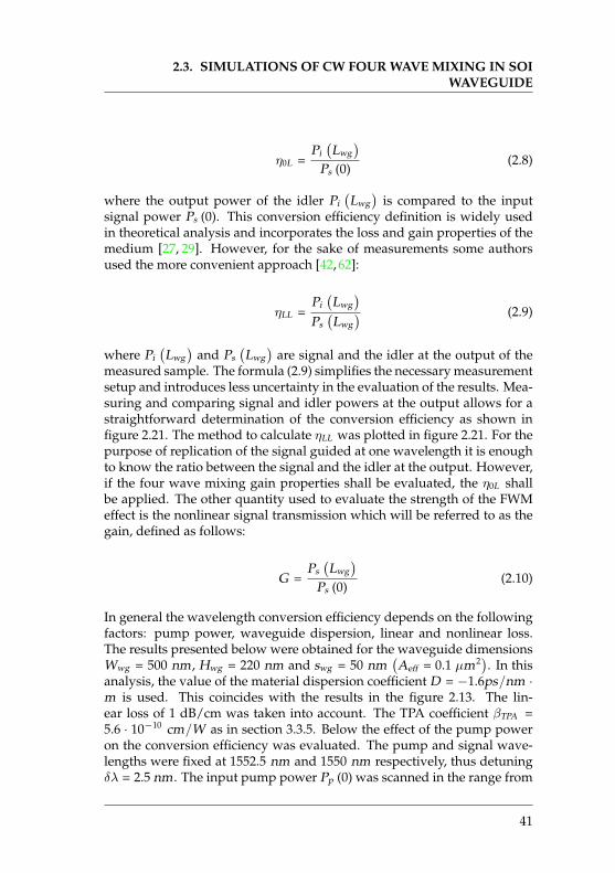
2.3. SIMULATIONS OF CW FOUR WAVE MIXING IN SOIWAVEGUIDE
η0L =Pi(Lwg
)Ps (0)
(2.8)
where the output power of the idler Pi(Lwg
)is compared to the input
signal power Ps (0). This conversion efficiency definition is widely usedin theoretical analysis and incorporates the loss and gain properties of themedium [27, 29]. However, for the sake of measurements some authorsused the more convenient approach [42, 62]:
ηLL =Pi(Lwg
)Ps(Lwg
) (2.9)
where Pi(Lwg
)and Ps
(Lwg
)are signal and the idler at the output of the
measured sample. The formula (2.9) simplifies the necessary measurementsetup and introduces less uncertainty in the evaluation of the results. Mea-suring and comparing signal and idler powers at the output allows for astraightforward determination of the conversion efficiency as shown infigure 2.21. The method to calculate ηLL was plotted in figure 2.21. For thepurpose of replication of the signal guided at one wavelength it is enoughto know the ratio between the signal and the idler at the output. However,if the four wave mixing gain properties shall be evaluated, the η0L shallbe applied. The other quantity used to evaluate the strength of the FWMeffect is the nonlinear signal transmission which will be referred to as thegain, defined as follows:
G =Ps(Lwg
)Ps (0)
(2.10)
In general the wavelength conversion efficiency depends on the followingfactors: pump power, waveguide dispersion, linear and nonlinear loss.The results presented below were obtained for the waveguide dimensionsWwg = 500 nm , Hwg = 220 nm and swg = 50 nm
(Aeff = 0.1 µm2). In this
analysis, the value of the material dispersion coefficient D = −1.6ps/nm ·m is used. This coincides with the results in the figure 2.13. The lin-ear loss of 1 dB/cm was taken into account. The TPA coefficient βTPA =5.6 · 10−10 cm/W as in section 3.3.5. Below the effect of the pump poweron the conversion efficiency was evaluated. The pump and signal wave-lengths were fixed at 1552.5 nm and 1550 nm respectively, thus detuningδλ = 2.5 nm . The input pump power Pp (0) was scanned in the range from
41
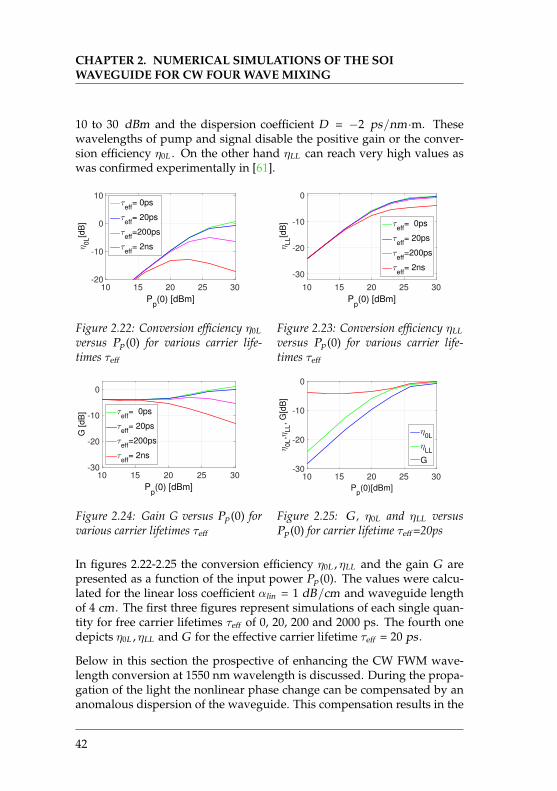
CHAPTER 2. NUMERICAL SIMULATIONS OF THE SOIWAVEGUIDE FOR CW FOUR WAVE MIXING
10 to 30 dBm and the dispersion coefficient D = −2 ps/nm·m. Thesewavelengths of pump and signal disable the positive gain or the conver-sion efficiency η0L . On the other hand ηLL can reach very high values aswas confirmed experimentally in [61].
Pp(0) [dBm]
10 15 20 25 30
η0
L[d
B]
-20
-10
0
10τ
eff= 0ps
τeff
= 20ps
τeff
=200ps
τeff
= 2ns
Figure 2.22: Conversion efficiency η0L
versus Pp (0) for various carrier life-times τeff
Pp(0) [dBm]
10 15 20 25 30η
LL[d
B]
-30
-20
-10
0
τeff
= 0ps
τeff
= 20ps
τeff
=200ps
τeff
= 2ns
Figure 2.23: Conversion efficiency ηLL
versus Pp (0) for various carrier life-times τeff
Pp(0) [dBm]
10 15 20 25 30
G [dB
]
-30
-20
-10
0
τeff
= 0ps
τeff
= 20ps
τeff
=200ps
τeff
= 2ns
Figure 2.24: Gain G versus Pp (0) forvarious carrier lifetimes τeff
Pp(0)[dBm]
10 15 20 25 30
η0
L,η
LL, G
[dB
]
-30
-20
-10
0
η0L
ηLL
G
Figure 2.25: G , η0L and ηLL versusPp (0) for carrier lifetime τeff =20ps
In figures 2.22-2.25 the conversion efficiency η0L , ηLL and the gain G arepresented as a function of the input power Pp (0). The values were calcu-lated for the linear loss coefficient αlin = 1 dB/cm and waveguide lengthof 4 cm . The first three figures represent simulations of each single quan-tity for free carrier lifetimes τeff of 0, 20, 200 and 2000 ps. The fourth onedepicts η0L , ηLL and G for the effective carrier lifetime τeff = 20 ps .
Below in this section the prospective of enhancing the CW FWM wave-length conversion at 1550 nm wavelength is discussed. During the propa-gation of the light the nonlinear phase change can be compensated by ananomalous dispersion of the waveguide. This compensation results in the
42
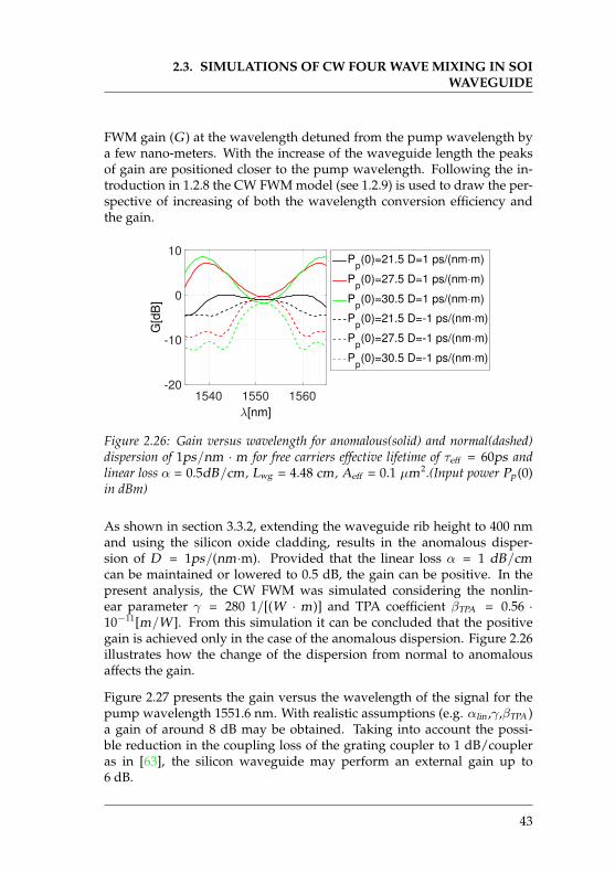
2.3. SIMULATIONS OF CW FOUR WAVE MIXING IN SOIWAVEGUIDE
FWM gain (G ) at the wavelength detuned from the pump wavelength bya few nano-meters. With the increase of the waveguide length the peaksof gain are positioned closer to the pump wavelength. Following the in-troduction in 1.2.8 the CW FWM model (see 1.2.9) is used to draw the per-spective of increasing of both the wavelength conversion efficiency andthe gain.
λ[nm]
1540 1550 1560
G[d
B]
-20
-10
0
10P
p(0)=21.5 D=1 ps/(nm·m)
Pp(0)=27.5 D=1 ps/(nm·m)
Pp(0)=30.5 D=1 ps/(nm·m)
Pp(0)=21.5 D=-1 ps/(nm·m)
Pp(0)=27.5 D=-1 ps/(nm·m)
Pp(0)=30.5 D=-1 ps/(nm·m)
Figure 2.26: Gain versus wavelength for anomalous(solid) and normal(dashed)dispersion of 1ps/nm · m for free carriers effective lifetime of τeff = 60ps andlinear loss α = 0.5dB/cm , Lwg = 4.48 cm , Aeff = 0.1 µm2.(Input power Pp (0)in dBm)
As shown in section 3.3.2, extending the waveguide rib height to 400 nmand using the silicon oxide cladding, results in the anomalous disper-sion of D = 1ps/(nm·m). Provided that the linear loss α = 1 dB/cmcan be maintained or lowered to 0.5 dB, the gain can be positive. In thepresent analysis, the CW FWM was simulated considering the nonlin-ear parameter γ = 280 1/[(W · m)] and TPA coefficient βTPA = 0.56 ·10−11[m/W ]. From this simulation it can be concluded that the positivegain is achieved only in the case of the anomalous dispersion. Figure 2.26illustrates how the change of the dispersion from normal to anomalousaffects the gain.
Figure 2.27 presents the gain versus the wavelength of the signal for thepump wavelength 1551.6 nm. With realistic assumptions (e.g. αlin ,γ,βTPA )a gain of around 8 dB may be obtained. Taking into account the possi-ble reduction in the coupling loss of the grating coupler to 1 dB/coupleras in [63], the silicon waveguide may perform an external gain up to6 dB.
43
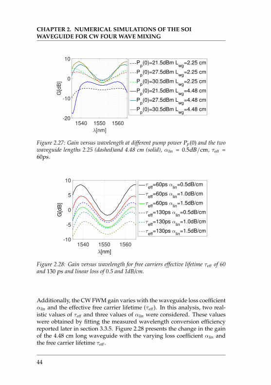
CHAPTER 2. NUMERICAL SIMULATIONS OF THE SOIWAVEGUIDE FOR CW FOUR WAVE MIXING
λ[nm]
1540 1550 1560
G[d
B]
-20
-10
0
10P
p(0)=21.5dBm L
wg=2.25 cm
Pp(0)=27.5dBm L
wg=2.25 cm
Pp(0)=30.5dBm L
wg=2.25 cm
Pp(0)=21.5dBm L
wg=4.48 cm
Pp(0)=27.5dBm L
wg=4.48 cm
Pp(0)=30.5dBm L
wg=4.48 cm
Figure 2.27: Gain versus wavelength at different pump power Pp (0) and the twowaveguide lengths 2.25 (dashed)and 4.48 cm (solid), αlin = 0.5dB/cm , τeff =60ps .
λ[nm]
1540 1550 1560
G[d
B]
-10
-5
0
5
10τ
eff=60ps α
lin=0.5dB/cm
τeff
=60ps αlin
=1.0dB/cm
τeff
=60ps αlin
=1.5dB/cm
τeff
=130ps αlin
=0.5dB/cm
τeff
=130ps αlin
=1.0dB/cm
τeff
=130ps αlin
=1.5dB/cm
Figure 2.28: Gain versus wavelength for free carriers effective lifetime τeff of 60and 130 ps and linear loss of 0.5 and 1dB/cm.
Additionally, the CW FWM gain varies with the waveguide loss coefficientαlin and the effective free carrier lifetime (τeff ). In this analysis, two real-istic values of τeff and three values of αlin were considered. These valueswere obtained by fitting the measured wavelength conversion efficiencyreported later in section 3.3.5. Figure 2.28 presents the change in the gainof the 4.48 cm long waveguide with the varying loss coefficient αlin andthe free carrier lifetime τeff .
44
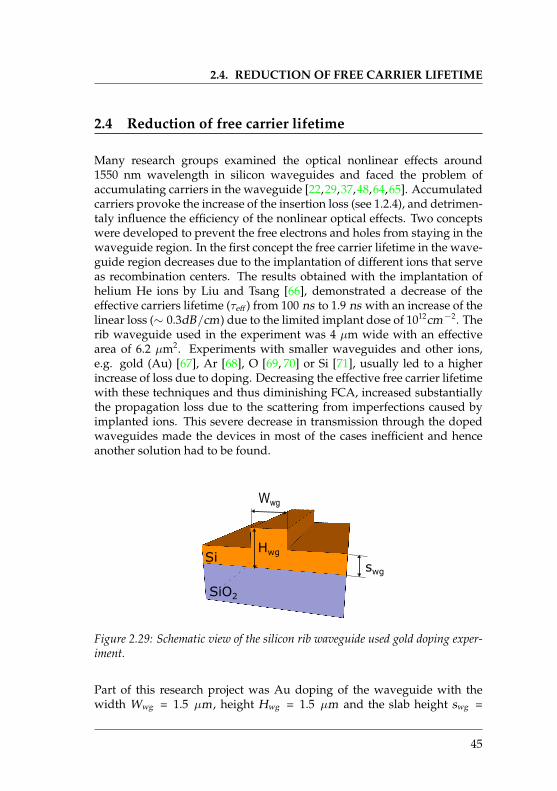
2.4. REDUCTION OF FREE CARRIER LIFETIME
2.4 Reduction of free carrier lifetime
Many research groups examined the optical nonlinear effects around1550 nm wavelength in silicon waveguides and faced the problem ofaccumulating carriers in the waveguide [22,29,37,48,64,65]. Accumulatedcarriers provoke the increase of the insertion loss (see 1.2.4), and detrimen-taly influence the efficiency of the nonlinear optical effects. Two conceptswere developed to prevent the free electrons and holes from staying in thewaveguide region. In the first concept the free carrier lifetime in the wave-guide region decreases due to the implantation of different ions that serveas recombination centers. The results obtained with the implantation ofhelium He ions by Liu and Tsang [66], demonstrated a decrease of theeffective carriers lifetime (τeff ) from 100 ns to 1.9 ns with an increase of thelinear loss (∼ 0.3dB/cm) due to the limited implant dose of 1012cm−2. Therib waveguide used in the experiment was 4 µm wide with an effectivearea of 6.2 µm2. Experiments with smaller waveguides and other ions,e.g. gold (Au) [67], Ar [68], O [69, 70] or Si [71], usually led to a higherincrease of loss due to doping. Decreasing the effective free carrier lifetimewith these techniques and thus diminishing FCA, increased substantiallythe propagation loss due to the scattering from imperfections caused byimplanted ions. This severe decrease in transmission through the dopedwaveguides made the devices in most of the cases inefficient and henceanother solution had to be found.
Si
SiO2
Wwg
swg
Hwg
Figure 2.29: Schematic view of the silicon rib waveguide used gold doping exper-iment.
Part of this research project was Au doping of the waveguide with thewidth Wwg = 1.5 µm , height Hwg = 1.5 µm and the slab height swg =
45
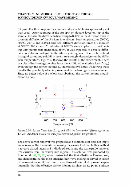
CHAPTER 2. NUMERICAL SIMULATIONS OF THE SOIWAVEGUIDE FOR CW FOUR WAVE MIXING
0.7 µm . For this purpose the commercially available Au spin-on-dopantwas used. After spinning of the Au spin-on-dopant layer on top of thesample, the samples have been heated up to 800◦C in the diffusion oven topromote diffusion of the Au ions into silicon. Four temperatures (500◦C,600◦C, 700◦C and 800◦C) and two different diffusion times (10 minutesat 500◦C, 700◦C and 20 minutes at 800◦C) were applied. Experiment-ing with parameters mentioned above it was expected to achieve differ-ent concentrations of gold in the silicon guiding layer. It must be noticedthat gold saturating solubility levels are strongly dependent on the diffu-sion temperature. Figure 2.30 shows the results of the experiment. Thereis a clear disadvantage coming from the additional scattering loss (∆αlin )even though the carrier lifetime τeff decreased five times. Following theseresults, the possibility of an improvement in the loss figure was examined.Since no better value of the loss was obtained, the carrier lifetime modifi-cation by Au diffusion was discontinued.
Temperature [oC]
400 500 600 700 800
∆α
lin [dB
/cm
]
0
1
2
3
400 500 600 700 800
τe
ff [ns]
0
2
4
6
Figure 2.30: Excess linear loss ∆αlin and effective free carrier lifetime τeff in the1.5 µm Au doped silicon rib waveguide versus diffusion temperature.
The active carrier removal was proposed as a solution, as it does not implyan increase of the loss while decreasing the carrier lifetime. In this methoda reverse biased lateral p-i-n diode placed along the waveguide removesfree carriers from the waveguide region. This solution was proposed byRong et al. [64, 72, 73], who constructed the first all-silicon Raman laser,and demonstrated the most efficient four wave mixing observed in silconrib waveguides until that time. Later Turner-Foster et al. proved exper-imentally that the effective carrier lifetime as short as 12 ps in a silicon
46
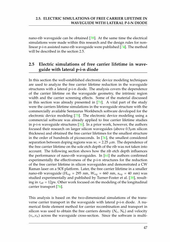
2.5. ELECTRIC SIMULATIONS OF FREE CARRIER LIFETIME INWAVEGUIDE WITH LATERAL P-I-N DIODE
nano-rib waveguide can be obtained [38]. At the same time the electricalsimulations were made within this research and the design rules for non-linear p-i-n assisted nano-rib waveguide were published [74]. The methodwill be described in the section 2.5.
2.5 Electric simulations of free carrier lifetime in wave-guide with lateral p-i-n diode
In this section the well-established electronic device modeling techniquesare used to analyze the free carrier lifetime reduction in the waveguidestructures with a lateral p-i-n diode. The analysis covers the dependenceof the carrier lifetime on the waveguide geometry, the intrinsic regionwidth and the carrier screening effects. Some of the material discussedin this section was already presented in [74]. A vital part of the studywere the carriers lifetime simulations in the waveguide structure with thecommercially available Sentaurus Workbench software developed for theelectronic device modeling [75]. The electronic device modeling using acommercial software was already applied to free carrier lifetime studiesin p-i-n waveguide structures [36]. In a prior work, however, the authorsfocused their research on larger silicon waveguides (above 0.5µm siliconthickness) and obtained the free carrier lifetimes for the smallest structurein the order of hundreds of picoseconds. In [36], the smallest consideredseparation between doping regions was wi = 2.25 µm . The dependence ofthe free carrier lifetime on the sole etch depth of the rib was not taken intoaccount. The following section shows how the rib etch depth influencesthe performance of nano-rib waveguides. In [64] the authors confirmedexperimentally the effectiveness of the p-i-n structures for the reductionof the free carrier lifetime in silicon waveguides and demonstrated a CWRaman laser on a SOI platform. Later, the free carrier lifetime in a smallernano-rib waveguide (Hwg = 295 nm , Wwg = 660 nm , swg = 40 nm) wasstudied experimentally and published by Turner-Foster et al. [38], result-ing in τeff = 12ps . Other work focused on the modeling of the longitudinalcarrier transport [76].
This analysis is based on the two-dimensional simulations of the trans-verse carrier transport in the waveguide with lateral p-i-n diode. A nu-merical finite element method for carrier recombination and transport insilicon was used to obtain the free carriers density (Ne , Nh ) and velocity(ve ,vh ) across the waveguide cross-section. Since the software is multi-
47
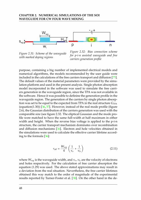
CHAPTER 2. NUMERICAL SIMULATIONS OF THE SOIWAVEGUIDE FOR CW FOUR WAVE MIXING
Wwg
wi
swgHwg
Figure 2.31: Scheme of the waveguidewith marked doping regions
p i n
+-
Figure 2.32: Bias connection schemefor p-i-n assisted waveguide and freecarriers generation profile
purpose, containing a big number of implemented electrical models andnumerical algorithms, the models recommended by the user guide wereincluded in the calculations of the free carriers transport and diffusion [75].The default values of the material parameters were provided by the simu-lation platform and used in the present analysis. Single photon absorptionmodel incorporated in the software was used to simulate the free carri-ers generation in the waveguide region, since the TPA was not available inthe software. Hence it was possible to definine the generation profile in thewaveguide region. The generation of the carriers by single photon absorp-tion was set to be equal to the expected from TPA in the real structure GTPA
(equation(1.30)) [36, 37]. However, instead of the real mode profile (figure2.6), the Gaussian distribution of the carriers generation was used with thecomparable size (see figure 2.32. The eliptical Gaussian and the mode pro-file were matched to have the same full-width at half maximum in eitherwidth and height. When the reverse bias voltage is applied to the p-i-nstructure, the carrier transport mechanism dominates over recombinationand diffusion mechanisms [36]. Electron and hole velocities obtained inthe simulations were used to calculate the effective carrier lifetime accord-ing to the formula [36]:
τeff =Wwg
4
(1ve
+1
vh
)(2.11)
where Wwg is the waveguide width, and ve , vh are the velocity of electronsand holes respectively. For the calculation of free carrier absorption theequation (1.29) was used. The above stated approximations may result ina deviation from the real situation. Nevertheless, the free carrier lifetimesobtained this way match to the order of magnitude of the experimentalresults reported by Turner-Foster et al. [38]. On the other hand in the de-
48
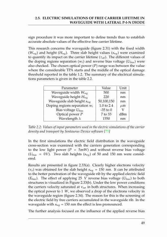
2.5. ELECTRIC SIMULATIONS OF FREE CARRIER LIFETIME INWAVEGUIDE WITH LATERAL P-I-N DIODE
sign procedure it was more important to define trends than to establishaccurate absolute values of the effective free carrier lifetime.
This research concerns the waveguide (figure 2.31) with the fixed width(Wwg ) and height (Hwg ). Three slab height values (swg ) were examinedto quantify its impact on the carrier lifetime (τeff ). The different values ofthe doping regions separation (wi ) and reverse bias voltage (Ubias ) werealso checked. The chosen optical power (P ) range was between the valuewhere the considerable TPA starts and the middle of the optical damagethreshold reported in the table 1.2. The summary of the electrical simula-tions parameters is given in the table 2.2.
Parameter Value UnitWaveguide width Wwg 500 nmWaveguide height Hwg 220 nm
Waveguide slab height swg 50,100,150 nmDoping regions separation wi 1.0 to 2.4 µm
Bias voltage Ubias -35 to 0 VOptical power P 7 to 33 dBm
Wavelength λ 1550 nm
Table 2.2: Values of input parameters used in the electric simulations of the carrierdensity and transport by Sentaurus Device software [75]
In the first simulations the electric field distribution in the waveguidecross-section was examined with the carriers generation correspondingto the low light power (P = 5mW ) and without reverse bias voltage(Ubias = 0V ). Two slab heights (swg ) of 50 and 150 nm were consid-ered.
Results are presented in figure 2.33(a). Clearly higher electrons velocity(ve ) was obtained for the slab height swg = 150 nm . It can be attributedto the better penetration of the waveguide rib by the applied electric field(Ebias ). The effect of applying 25 V reverse bias voltage (Ubias ) to bothstructures is visualized in Figure 2.33(b). Under the low power conditionsthe carriers velocity saturated at vsat in both structures. When increasingthe optical power to 1 W , we observed a drop of the electrons velocity inthe waveguide region (figure 2.34). The reason for this is the screening ofthe electric field by free carriers accumulated in the waveguide rib. In thewaveguide with swg = 150 nm the effect is less pronounced.
The further analysis focused on the influence of the applied reverse bias
49
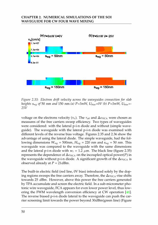
CHAPTER 2. NUMERICAL SIMULATIONS OF THE SOIWAVEGUIDE FOR CW FOUR WAVE MIXING
ve[cm/s]
((a) (b)
swg = 50nm
swg = 150nm
swg = 50nm
swg = 150nm
Figure 2.33: Electron drift velocity across the waveguides crossection for slabheights swg of 50 nm and 150 nm .(a) P=5mW, Ubias =0V (b) P=5mW, Ubias =-25V
voltage on the electrons velocity (ve ). The τeff and ∆αFCA were chosen asmeasures of the free carriers sweep efficiency. Two types of waveguideswere considered: with the lateral p-i-n diode and without (simple wave-guide). The waveguide with the lateral p-i-n diode was examined withdifferent levels of the reverse bias voltage. Figures 2.35 and 2.36 show theadvantage of using the lateral diode. The simple waveguide, had the fol-lowing dimensions Wwg = 500nm , Hwg = 220 nm and swg = 50 nm . Thiswaveguide was compared to the waveguide with the same dimensionsand the lateral p-i-n diode with wi = 1.2 µm . The black line (figure 2.35)represents the dependence of ∆αFCA on the incoupled optical power(P ) inthe waveguide without p-i-n diode. A significant growth of the ∆αFCA isobserved already at P = 21dBm .
The built-in electric field (red line, 0V bias) introduced solely by the dop-ing regions sweeps the free carriers away. Therefore, the ∆αFCA -rise shiftstowards 25 dBm . However, above this power the free carriers generatedby TPA accumulate and screen the electric field. In a sub-micrometer pho-tonic wire waveguide, FCA appears for even lower power level, thus low-ering the FWM wavelength conversion efficiency at CW operation [48].The reverse biased p-i-n diode lateral to the waveguide can push the car-rier screening limit towards the power beyond 30dBm(green line) (Figure
50
2.5. ELECTRIC SIMULATIONS OF FREE CARRIER LIFETIME INWAVEGUIDE WITH LATERAL P-I-N DIODE
ve[cm/s]
Figure 2.34: Electron drift velocity decrease, due to carriers screening, across thewaveguide crossection for slab heights swg of 50 nm(left) and 150 nm(right),power P = 1 W and bias Ubias = −25 V .
10 20 300
10
20
30
40
50
P [dBm]
FC
A[d
B/c
m]
w/o pin
0V
3V
5V
10V
20VΔα
FC
A [dB
/cm
]
Figure 2.35: Excess free carrier loss co-efficient ∆αFCA versus P in the wave-guide for different Ubias (wi = 1.2 µm ,swg = 50 nm).
10 20 30 4010 12
10 11
10 10
10 09
P [dBm]
avg[s]
w/o pin
0V
3V
5V
10V
20V
τeff�[ps]
Figure 2.36: Free carrier lifetime τeff
versus P in the waveguide for differentUbias ,(wi = 1.2 µm , swg = 50 nm ).
2.36). Nonetheless, the reverse Ubias is limited by the breakdown voltageas expressed below:
VBD = EBD · wi (2.12)
where EBD = 2.5 · 105V/cm is the breakdown field of silicon and wi is thewidth of the intrinsic region [24]. The breakdown voltage of the structuresanalyzed in this work varies from 20 V to 40 V . The shortest carrier life-time shown in figure 2.36 results from the maximum drift velocity of freecarriers vsat (for both electrons and holes the same [24]) and can be esti-mated from:
51
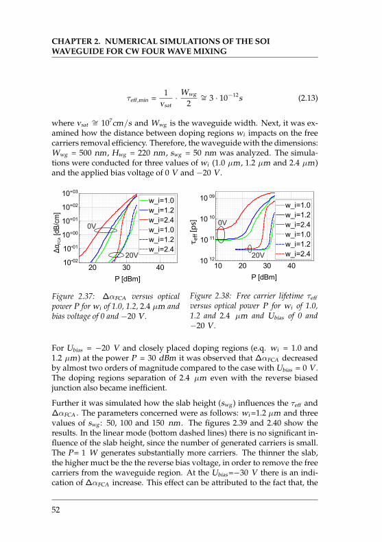
CHAPTER 2. NUMERICAL SIMULATIONS OF THE SOIWAVEGUIDE FOR CW FOUR WAVE MIXING
τeff ,min =1
vsat·
Wwg
2∼= 3 · 10−12s (2.13)
where vsat ∼= 107cm/s and Wwg is the waveguide width. Next, it was ex-amined how the distance between doping regions wi impacts on the freecarriers removal efficiency. Therefore, the waveguide with the dimensions:Wwg = 500 nm , Hwg = 220 nm , swg = 50 nm was analyzed. The simula-tions were conducted for three values of wi (1.0 µm , 1.2 µm and 2.4 µm)and the applied bias voltage of 0 V and −20 V .
20 30 4010 02
10 01
10+00
10+01
10+02
10+03
P [dBm]
FC
A[d
B/c
m]
w_i=1.0
w_i=1.2
w_i=2.4
w_i=1.0
w_i=1.2
w_i=2.4
0V
20V
Δα
FC
A [dB
/cm
]
-
-
Figure 2.37: ∆αFCA versus opticalpower P for wi of 1.0, 1.2, 2.4 µm andbias voltage of 0 and −20 V .
10 20 30 4010 12
10 11
10 10
10 09
P [dBm]
w_i=1.0
w_i=1.2
w_i=2.4
w_i=1.0
w_i=1.2
w_i=2.4
τeff�[ps]
20V
0V
Figure 2.38: Free carrier lifetime τeff
versus optical power P for wi of 1.0,1.2 and 2.4 µm and Ubias of 0 and−20 V .
For Ubias = −20 V and closely placed doping regions (e.q. wi = 1.0 and1.2 µm) at the power P = 30 dBm it was observed that ∆αFCA decreasedby almost two orders of magnitude compared to the case with Ubias = 0 V .The doping regions separation of 2.4 µm even with the reverse biasedjunction also became inefficient.
Further it was simulated how the slab height (swg ) influences the τeff and∆αFCA . The parameters concerned were as follows: wi =1.2 µm and threevalues of swg : 50, 100 and 150 nm . The figures 2.39 and 2.40 show theresults. In the linear mode (bottom dashed lines) there is no significant in-fluence of the slab height, since the number of generated carriers is small.The P= 1 W generates substantially more carriers. The thinner the slab,the higher muct be the the reverse bias voltage, in order to remove the freecarriers from the waveguide region. At the Ubias =−30 V there is an indi-cation of ∆αFCA increase. This effect can be attributed to the fact that, the
52
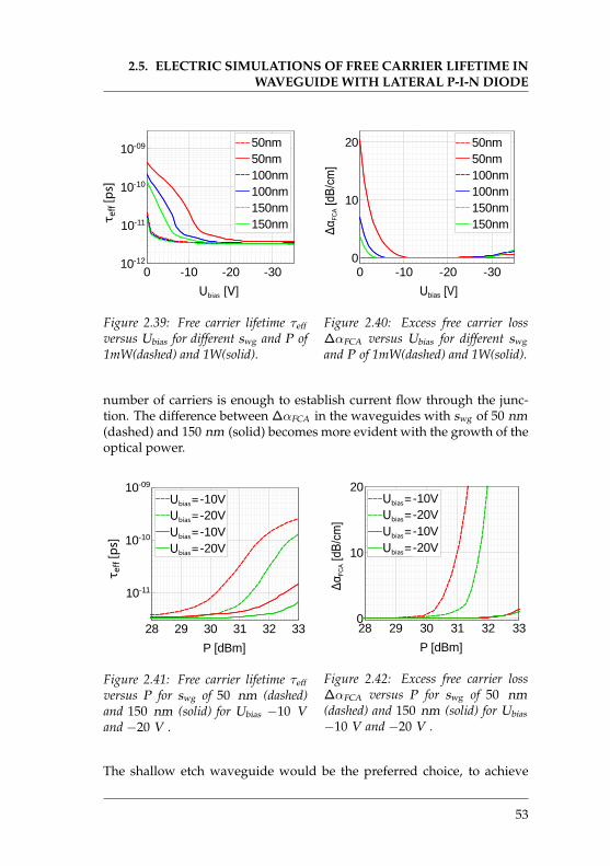
2.5. ELECTRIC SIMULATIONS OF FREE CARRIER LIFETIME INWAVEGUIDE WITH LATERAL P-I-N DIODE
τeff�[ps]
Ubias�[V]
Figure 2.39: Free carrier lifetime τeff
versus Ubias for different swg and P of1mW(dashed) and 1W(solid).
Δα
FC
A[d
B/c
m]
Ubias [V]
Figure 2.40: Excess free carrier loss∆αFCA versus Ubias for different swg
and P of 1mW(dashed) and 1W(solid).
number of carriers is enough to establish current flow through the junc-tion. The difference between ∆αFCA in the waveguides with swg of 50 nm(dashed) and 150 nm (solid) becomes more evident with the growth of theoptical power.
τeff�[ps]
Ubias=
Ubias=
Ubias=
Ubias=
Figure 2.41: Free carrier lifetime τeff
versus P for swg of 50 nm (dashed)and 150 nm (solid) for Ubias −10 Vand −20 V .
Δα
FC
A [
dB
/cm
]
Ubias=
Ubias=
Ubias=
Ubias=
Figure 2.42: Excess free carrier loss∆αFCA versus P for swg of 50 nm(dashed) and 150 nm (solid) for Ubias
−10 V and −20 V .
The shallow etch waveguide would be the preferred choice, to achieve
53
CHAPTER 2. NUMERICAL SIMULATIONS OF THE SOIWAVEGUIDE FOR CW FOUR WAVE MIXING
an efficient carriers sweeping from the waveguide region. It enables theefficient free carrier removal at high optical powers. However, this wa-veguide exhibits high normal dispersion as presented in the section 2.2.3,that results in the very narrow FWM bandwidth. Although absolute val-ues extracted from the CW measurement reported further in this thesis3.3.5 differ by one up to two orders of magnitude from the presented here.This may be caused by the samples imperfections e.g. lower then expectedvoltage in the waveguide in the realized structures. Eventually the addi-tional effects that were not taken into account in the simulations occurredin the real samples. Although the absolute values of τeff may be underesti-mated, the trends obtained with this method led to the optimization of thenonlinear waveguide with lateral p-i-n diode.
From the simulation results discussed in chapter 2 it is clear, that a compro-mise needs to be found between a demand for the anomalous dispersionand the free carriers sweeping efficiency (τeff < 10 ps). The first requireshigh (Hwg > 220 nm) and deeply etched waveguide (swg = 50 nm) whilethe latter would promote use of the shallow etching (swg ≈ 150 nm).The shallow etching proved also to be an ideal method to keep the wa-veguide loss very low [52]. This would help in reaching gain, providedthat the anomalous dispersion was obtained. However the shallow etch-ing of the waveguide determines the high normal dispersion. The broad-band and highly efficient wavelength conversion (see equations (1.56) and(1.58)) can be obtained only if the anomalous dispersion regime is pro-vided. Moreover, the efficient wavelength conversion and the gain can beobtained only if the linear loss is suppressed (αlin < 1dB/cm). It is alsoworth mentioning that the cross-section of the waveguide is considerablysmaller then the fiber core. An efficient incoupling scheme must also beensured to avoid the loss at the interface fiber-to-waveguide. This issuewill be addressed in the section 3.2.
54
3Design, fabrication and characterization of
samples
The integration of the p-i-n lateral diode along the nano-rib waveguide isbeneficial for the nonlinear optical applications. This was discussed in sec-tions 1.2.4, 1.2.8 and 2.5. The electrical simulations presented in section 2.5proved that the smaller the separation is between the doping areas wi themore efficient is removal of free carriers i.e. the lower the loss from the TPAinduced FCA. In this chapter the fabrication process of the samples is in-troduced. It is described which challenges stand still on the way towardsthe realization of a silicon nano-rib waveguide for the FWM process. Insection 3.1 the design process of the samples shall be presented. Later inthe section 3.2 the fabrication process will be discussed, emphasizing thechallenges in the production and some potential improvements that canbe applied in the future. In section 3.3 the results of the characterizationof the waveguides will be presented. Firstly, the electrical and optoelec-trical characteristics of the waveguide with p-i-n diode will be measuredin section 3.3.1. The description of the dispersion measurement will bepresented in section 3.3.2. In section 3.3.3 the linear optical characteris-tics will be determined. The measurement of the dependence of the linearoptical loss on the applied bias voltage will be described in section 3.3.4.Moreover, it will shown how the p-i-n diode influence the propagation ofthe light in the waveguide. Later in section 3.3.5 the measurement of thepower dependent loss originating from TPA and TPA induced FCA willbe reported. The CW four wave mixing measurements are described insection 3.3.6. In section 3.3.7 the phase sensitive amplification (PSA) forthe wavelengths around 1550 nm will be demonstrated.
55
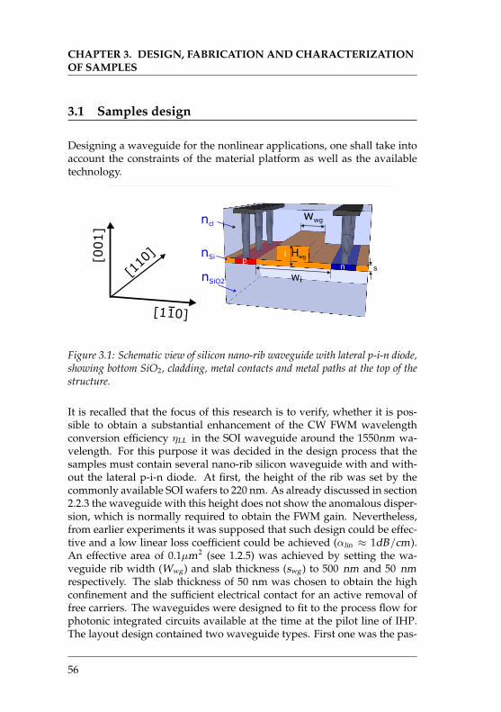
CHAPTER 3. DESIGN, FABRICATION AND CHARACTERIZATIONOF SAMPLES
3.1 Samples design
Designing a waveguide for the nonlinear applications, one shall take intoaccount the constraints of the material platform as well as the availabletechnology.
wwg
Hwg
nSiO2
nSi
ncl
wi
[001]
[110]
[110]-
Figure 3.1: Schematic view of silicon nano-rib waveguide with lateral p-i-n diode,showing bottom SiO2, cladding, metal contacts and metal paths at the top of thestructure.
It is recalled that the focus of this research is to verify, whether it is pos-sible to obtain a substantial enhancement of the CW FWM wavelengthconversion efficiency ηLL in the SOI waveguide around the 1550nm wa-velength. For this purpose it was decided in the design process that thesamples must contain several nano-rib silicon waveguide with and with-out the lateral p-i-n diode. At first, the height of the rib was set by thecommonly available SOI wafers to 220 nm. As already discussed in section2.2.3 the waveguide with this height does not show the anomalous disper-sion, which is normally required to obtain the FWM gain. Nevertheless,from earlier experiments it was supposed that such design could be effec-tive and a low linear loss coefficient could be achieved (αlin ≈ 1dB/cm).An effective area of 0.1µm2 (see 1.2.5) was achieved by setting the wa-veguide rib width (Wwg ) and slab thickness (swg ) to 500 nm and 50 nmrespectively. The slab thickness of 50 nm was chosen to obtain the highconfinement and the sufficient electrical contact for an active removal offree carriers. The waveguides were designed to fit to the process flow forphotonic integrated circuits available at the time at the pilot line of IHP.The layout design contained two waveguide types. First one was the pas-
56
3.1. SAMPLES DESIGN
sive waveguides without p-i-n junction carrier removal. The second typecontained p (boron) and n (arsenic) doping regions on the sides with dop-ing concentrations of NA = 5 · 1017 cm−3 and ND = 3 · 1018 cm−3 respec-tively. These concentrations were required by the other structures realizedon the same wafer. The other structures are irrelevant for this thesis. Nev-ertheless, the doping concentrations were suitable also for the free carrierremoval scheme. In order to provide a good electrical contact within the pand n regions, the highly doped regions were created (NA = ND = 1020).Next the cobalt silicide was formed on top of the highly doped areas. Thecobalt silicide regions were electrically connected with the metal lines andpads via tungsten plugs distributed along them. The designed mask con-sist of the waveguides without doping regions on the side with lengths Lwg
of: 1.52 cm , 1.9 cm , 2.37 cm , 2.87 cm , 4.74 cm . The lengths of the wave-guides with lateral p-i-n diode were Lwg 1.7 cm , 2.25 cm and 4.48 cm . Thedimensions of the waveguides are summarized in the Table 3.1.
Waveguidetype
Length (Lwg )[cm]
wi
[nm]Wwg
[nm]Hwg
[nm]
no p-i-n 1.52, 1.9, 2.37, 2.87, 4.74 – 500 220p-i-n 1.7, 2.25, 4.48 1.2 500 220
Table 3.1: Dimensions of the designed waveguides
The design of the p-i-n waveguides must take into account different andsometimes contradictory requirements. On the one hand the electricalscheme should be efficient (low τeff for a relatively low reverse Ubias ). Thisrequires a relatively high slab (see section 2.5). On the other hand for theenhancement of the FWM the anomalous dispersion is necessary and thuslow slab height would be of advantage (see section 2.2.3. Therefore a com-promising solution had to be found. To fulfill these requirements severaloptical and electrical simulations were performed. The simulations per-formed in section 2.5 suggests that the smaller the distance between dop-ing regions (wi ) the better. How the separation of the doping regions in-fluences the propagation loss was discussed in section 2.2.4. As result theminimum possible width of the intrinsic waveguide region was defined(wi = 1.2 µm).
57
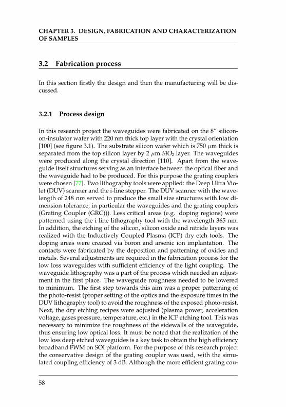
CHAPTER 3. DESIGN, FABRICATION AND CHARACTERIZATIONOF SAMPLES
3.2 Fabrication process
In this section firstly the design and then the manufacturing will be dis-cussed.
3.2.1 Process design
In this research project the waveguides were fabricated on the 8” silicon-on-insulator wafer with 220 nm thick top layer with the crystal orientation[100] (see figure 3.1). The substrate silicon wafer which is 750 µm thick isseparated from the top silicon layer by 2 µm SiO2 layer. The waveguideswere produced along the crystal direction [110]. Apart from the wave-guide itself structures serving as an interface between the optical fiber andthe waveguide had to be produced. For this purpose the grating couplerswere chosen [77]. Two lithography tools were applied: the Deep Ultra Vio-let (DUV) scanner and the i-line stepper. The DUV scanner with the wave-length of 248 nm served to produce the small size structures with low di-mension tolerance, in particular the waveguides and the grating couplers(Grating Coupler (GRC))). Less critical areas (e.g. doping regions) werepatterned using the i-line lithography tool with the wavelength 365 nm.In addition, the etching of the silicon, silicon oxide and nitride layers wasrealized with the Inductively Coupled Plasma (ICP) dry etch tools. Thedoping areas were created via boron and arsenic ion implantation. Thecontacts were fabricated by the deposition and patterning of oxides andmetals. Several adjustments are required in the fabrication process for thelow loss waveguides with sufficient efficiency of the light coupling. Thewaveguide lithography was a part of the process which needed an adjust-ment in the first place. The waveguide roughness needed to be loweredto minimum. The first step towards this aim was a proper patterning ofthe photo-resist (proper setting of the optics and the exposure times in theDUV lithography tool) to avoid the roughness of the exposed photo-resist.Next, the dry etching recipes were adjusted (plasma power, accelerationvoltage, gases pressure, temperature, etc.) in the ICP etching tool. This wasnecessary to minimize the roughness of the sidewalls of the waveguide,thus ensuring low optical loss. It must be noted that the realization of thelow loss deep etched waveguides is a key task to obtain the high efficiencybroadband FWM on SOI platform. For the purpose of this research projectthe conservative design of the grating coupler was used, with the simu-lated coupling efficiency of 3 dB. Although the more efficient grating cou-
58
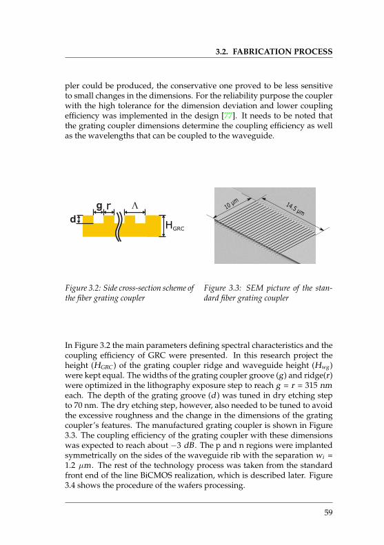
3.2. FABRICATION PROCESS
pler could be produced, the conservative one proved to be less sensitiveto small changes in the dimensions. For the reliability purpose the couplerwith the high tolerance for the dimension deviation and lower couplingefficiency was implemented in the design [77]. It needs to be noted thatthe grating coupler dimensions determine the coupling efficiency as wellas the wavelengths that can be coupled to the waveguide.
HGRC
Figure 3.2: Side cross-section scheme ofthe fiber grating coupler
14.5 µm10 µm
Figure 3.3: SEM picture of the stan-dard fiber grating coupler
In Figure 3.2 the main parameters defining spectral characteristics and thecoupling efficiency of GRC were presented. In this research project theheight (HGRC ) of the grating coupler ridge and waveguide height (Hwg )were kept equal. The widths of the grating coupler groove (g) and ridge(r)were optimized in the lithography exposure step to reach g = r = 315 nmeach. The depth of the grating groove (d ) was tuned in dry etching stepto 70 nm. The dry etching step, however, also needed to be tuned to avoidthe excessive roughness and the change in the dimensions of the gratingcoupler’s features. The manufactured grating coupler is shown in Figure3.3. The coupling efficiency of the grating coupler with these dimensionswas expected to reach about −3 dB . The p and n regions were implantedsymmetrically on the sides of the waveguide rib with the separation wi =1.2 µm . The rest of the technology process was taken from the standardfront end of the line BiCMOS realization, which is described later. Figure3.4 shows the procedure of the wafers processing.
59
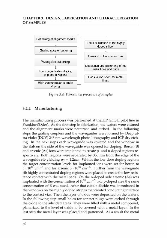
CHAPTER 3. DESIGN, FABRICATION AND CHARACTERIZATIONOF SAMPLES
Figure 3.4: Fabrication procedure of samples
3.2.2 Manufacturing
The manufacturing process was performed at theIHP GmbH pilot line inFrankfurt(Oder). As the first step in fabrication, the wafers were cleanedand the alignment marks were patterned and etched. In the followingsteps the grating couplers and the waveguides were formed by Deep ul-tra violet (DUV) 248 nm wavelength photo-lithography and ICP dry etch-ing. In the next steps each waveguide was covered and the window inthe slab on the side of the waveguide was opened for doping. Boron (B)and arsenic (As) ions were implanted to create p- and n-doped regions re-spectively. Both regions were separated by 350 nm from the edge of thewaveguide rib yielding wi = 1.2µm . Within the low dose doping regionsthe target concentration levels for implanted ions were set for boron to5 · 1017 cm−3 and for arsenic 3 · 1018 cm−3. Further from the waveguiderib highly concentrated doping regions were placed to create the low resis-tance contact with the metal pads. On the n-doped side arsenic (As) wasimplanted with the concentration of 1020 cm−3. For p-doped area the sameconcentration of B was used. After that cobalt silicide was introduced inthe windows on the highly doped stripes that created conducting interfaceto the contact vias. Then the layer of oxide were deposited on the wafers.In the following step small holes for contact plugs were etched throughthe oxide to the silicided areas. They were filled with a metal compound,planarized to the level of oxide to be covered with a metal layer. In thelast step the metal layer was placed and patterned. As a result the metal
60
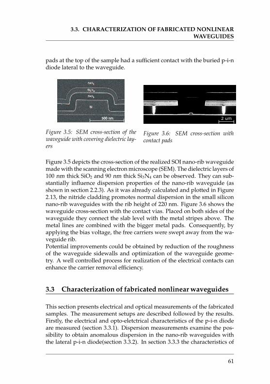
3.3. CHARACTERIZATION OF FABRICATED NONLINEARWAVEGUIDES
pads at the top of the sample had a sufficient contact with the buried p-i-ndiode lateral to the waveguide.
500 nm
Figure 3.5: SEM cross-section of thewaveguide with covering dielectric lay-ers
2 um
Figure 3.6: SEM cross-section withcontact pads
Figure 3.5 depicts the cross-section of the realized SOI nano-rib waveguidemade with the scanning electron microscope (SEM). The dielectric layers of100 nm thick SiO2 and 90 nm thick Si3N4 can be observed. They can sub-stantially influence dispersion properties of the nano-rib waveguide (asshown in section 2.2.3). As it was already calculated and plotted in Figure2.13, the nitride cladding promotes normal dispersion in the small siliconnano-rib waveguides with the rib height of 220 nm. Figure 3.6 shows thewaveguide cross-section with the contact vias. Placed on both sides of thewaveguide they connect the slab level with the metal stripes above. Themetal lines are combined with the bigger metal pads. Consequently, byapplying the bias voltage, the free carriers were swept away from the wa-veguide rib.Potential improvements could be obtained by reduction of the roughnessof the waveguide sidewalls and optimization of the waveguide geome-try. A well controlled process for realization of the electrical contacts canenhance the carrier removal efficiency.
3.3 Characterization of fabricated nonlinear waveguides
This section presents electrical and optical measurements of the fabricatedsamples. The measurement setups are described followed by the results.Firstly, the electrical and opto-eletctrical characteristics of the p-i-n diodeare measured (section 3.3.1). Dispersion measurements examine the pos-sibility to obtain anomalous dispersion in the nano-rib waveguides withthe lateral p-i-n diode(section 3.3.2). In section 3.3.3 the characteristics of
61
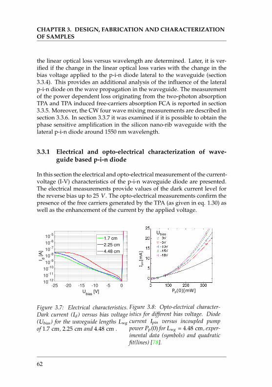
CHAPTER 3. DESIGN, FABRICATION AND CHARACTERIZATIONOF SAMPLES
the linear optical loss versus wavelength are determined. Later, it is ver-ified if the change in the linear optical loss varies with the change in thebias voltage applied to the p-i-n diode lateral to the waveguide (section3.3.4). This provides an additional analysis of the influence of the lateralp-i-n diode on the wave propagation in the waveguide. The measurementof the power dependent loss originating from the two-photon absorptionTPA and TPA induced free-carriers absorption FCA is reported in section3.3.5. Moreover, the CW four wave mixing measurements are described insection 3.3.6. In section 3.3.7 it was examined if it is possible to obtain thephase sensitive amplification in the silicon nano-rib waveguide with thelateral p-i-n diode around 1550 nm wavelength.
3.3.1 Electrical and opto-electrical characterization of wave-guide based p-i-n diode
In this section the electrical and opto-electrical measurement of the current-voltage (I-V) characteristics of the p-i-n waveguide diode are presented.The electrical measurements provide values of the dark current level forthe reverse bias up to 25 V . The opto-electrical measurements confirm thepresence of the free carriers generated by the TPA (as given in eq. 1.30) aswell as the enhancement of the current by the applied voltage.
Ubias
[V]
-25 -20 -15 -10 -5 0
I d [
A]
10-12
10-11
10-10
10-9
10-8
10-7
10-6
10-5
1.7 cm
2.25 cm
4.48 cm
Figure 3.7: Electrical characteristics.Dark current (Id ) versus bias voltage(Ubias ) for the waveguide lengths Lwg
of 1.7 cm , 2.25 cm and 4.48 cm .
I pin[mA]
Pp(0)[mW]
Ubias
-
-
-
-
Figure 3.8: Opto-electrical character-istics for different bias voltage. Diodecurrent Ipin versus incoupled pumppower Pp (0) for Lwg = 4.48 cm , exper-imental data (symbols) and quadraticfit(lines) [78].
62
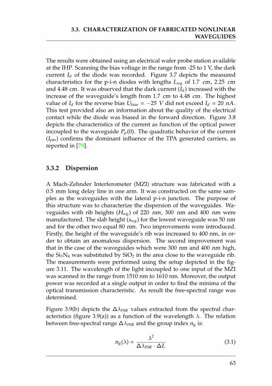
3.3. CHARACTERIZATION OF FABRICATED NONLINEARWAVEGUIDES
The results were obtained using an electrical wafer probe station availableat the IHP. Scanning the bias voltage in the range from -25 to 1 V, the darkcurrent Id of the diode was recorded. Figure 3.7 depicts the measuredcharacteristics for the p-i-n diodes with lengths Lwg of 1.7 cm , 2.25 cmand 4.48 cm . It was observed that the dark current (Id ) increased with theincrease of the waveguide’s length from 1.7 cm to 4.48 cm . The highestvalue of Id for the reverse bias Ubias = −25 V did not exceed Id = 20 nA .This test provided also an information about the quality of the electricalcontact while the diode was biased in the forward direction. Figure 3.8depicts the characteristics of the current as function of the optical powerincoupled to the waveguide Pp (0). The quadratic behavior of the current(Ipin ) confirms the dominant influence of the TPA generated carriers, asreported in [79].
3.3.2 Dispersion
A Mach-Zehnder Interferometer (MZI) structure was fabricated with a0.5 mm long delay line in one arm. It was constructed on the same sam-ples as the waveguides with the lateral p-i-n junction. The purpose ofthis structure was to characterize the dispersion of the waveguides. Wa-veguides with rib heights (Hwg ) of 220 nm , 300 nm and 400 nm weremanufactured. The slab height (swg ) for the lowest waveguide was 50 nmand for the other two equal 80 nm . Two improvements were introduced.Firstly, the height of the waveguide’s rib was increased to 400 nm, in or-der to obtain an anomalous dispersion. The second improvement wasthat in the case of the waveguides which were 300 nm and 400 nm high,the Si3N4 was substituted by SiO2 in the area close to the waveguide rib.The measurements were performed using the setup depicted in the fig-ure 3.11. The wavelength of the light incoupled to one input of the MZIwas scanned in the range from 1510 nm to 1610 nm. Moreover, the outputpower was recorded at a single output in order to find the minima of theoptical transmission characteristic. As result the free-spectral range wasdetermined.
Figure 3.9(b) depicts the ∆λFSR values extracted from the spectral char-acteristics (figure 3.9(a)) as a function of the wavelength λ. The relationbetween free-spectral range ∆λFSR and the group index ng is:
ng (λ) =λ2
∆λFSR ·∆L(3.1)
63
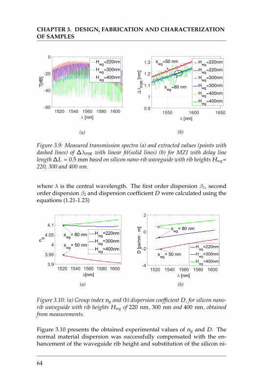
CHAPTER 3. DESIGN, FABRICATION AND CHARACTERIZATIONOF SAMPLES
λ [nm]
1520 1540 1560 1580 1600
T[d
B]
-60
-40
-20
0H
wg=220nm
Hwg
=300nm
Hwg
=400nm
(a)
λ [nm]
1550 1600 1650
∆λ
FS
R [
nm
]
0.9
1
1.1
1.2
1.3 Hwg
=220nm
Hwg
=220nm
Hwg
=300nm
Hwg
=300nm
Hwg
=400nm
Hwg
=400nm
swg
=80 nm
swg
=50 nm
(b)
Figure 3.9: Measured transmission spectra (a) and extracted values (points withdashed lines) of ∆λFSR with linear fit(solid lines) (b) for MZI with delay linelength ∆L = 0.5 mm based on silicon nano-rib waveguide with rib heights Hwg =220, 300 and 400 nm.
where λ is the central wavelength. The first order dispersion β1, secondorder dispersion β2 and dispersion coefficient D were calculated using theequations (1.21-1.23)
(a) (b)
Figure 3.10: (a) Group index ng and (b) dispersion coefficient D , for silicon nano-rib waveguide with rib heights Hwg of 220 nm , 300 nm and 400 nm , obtainedfrom measurements.
Figure 3.10 presents the obtained experimental values of ng and D . Thenormal material dispersion was successfully compensated with the en-hancement of the waveguide rib height and substitution of the silicon ni-
64
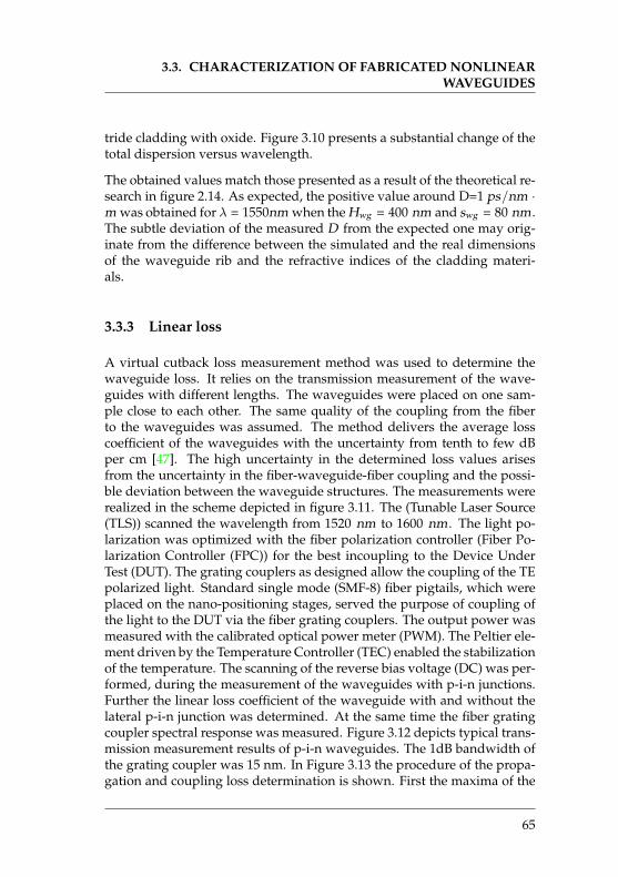
3.3. CHARACTERIZATION OF FABRICATED NONLINEARWAVEGUIDES
tride cladding with oxide. Figure 3.10 presents a substantial change of thetotal dispersion versus wavelength.
The obtained values match those presented as a result of the theoretical re-search in figure 2.14. As expected, the positive value around D=1 ps/nm ·m was obtained for λ = 1550nm when the Hwg = 400 nm and swg = 80 nm .The subtle deviation of the measured D from the expected one may orig-inate from the difference between the simulated and the real dimensionsof the waveguide rib and the refractive indices of the cladding materi-als.
3.3.3 Linear loss
A virtual cutback loss measurement method was used to determine thewaveguide loss. It relies on the transmission measurement of the wave-guides with different lengths. The waveguides were placed on one sam-ple close to each other. The same quality of the coupling from the fiberto the waveguides was assumed. The method delivers the average losscoefficient of the waveguides with the uncertainty from tenth to few dBper cm [47]. The high uncertainty in the determined loss values arisesfrom the uncertainty in the fiber-waveguide-fiber coupling and the possi-ble deviation between the waveguide structures. The measurements wererealized in the scheme depicted in figure 3.11. The (Tunable Laser Source(TLS)) scanned the wavelength from 1520 nm to 1600 nm . The light po-larization was optimized with the fiber polarization controller (Fiber Po-larization Controller (FPC)) for the best incoupling to the Device UnderTest (DUT). The grating couplers as designed allow the coupling of the TEpolarized light. Standard single mode (SMF-8) fiber pigtails, which wereplaced on the nano-positioning stages, served the purpose of coupling ofthe light to the DUT via the fiber grating couplers. The output power wasmeasured with the calibrated optical power meter (PWM). The Peltier ele-ment driven by the Temperature Controller (TEC) enabled the stabilizationof the temperature. The scanning of the reverse bias voltage (DC) was per-formed, during the measurement of the waveguides with p-i-n junctions.Further the linear loss coefficient of the waveguide with and without thelateral p-i-n junction was determined. At the same time the fiber gratingcoupler spectral response was measured. Figure 3.12 depicts typical trans-mission measurement results of p-i-n waveguides. The 1dB bandwidth ofthe grating coupler was 15 nm. In Figure 3.13 the procedure of the propa-gation and coupling loss determination is shown. First the maxima of the
65
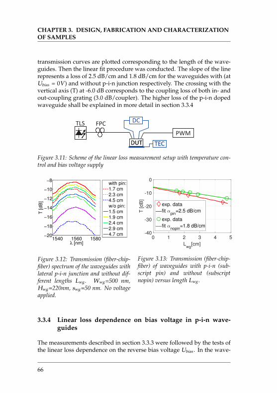
CHAPTER 3. DESIGN, FABRICATION AND CHARACTERIZATIONOF SAMPLES
transmission curves are plotted corresponding to the length of the wave-guides. Then the linear fit procedure was conducted. The slope of the linerepresents a loss of 2.5 dB/cm and 1.8 dB/cm for the waveguides with (atUbias = 0V ) and without p-i-n junction respectively. The crossing with thevertical axis (T) at -6.0 dB corresponds to the coupling loss of both in- andout-coupling grating (3.0 dB/coupler). The higher loss of the p-i-n dopedwaveguide shall be explained in more detail in section 3.3.4
TLS
PWM
DUT
FPC
DUT
DC
TEC
Figure 3.11: Scheme of the linear loss measurement setup with temperature con-trol and bias voltage supply
1540 1560 1580−20
−18
−16
−14
−12
−10
λ [nm]
T [dB
]
−8with pin:1.7 cm2.3 cm4.5 cmw/o pin:1.5 cm1.9 cm2.4 cm2.9 cm4.7 cm
Figure 3.12: Transmission (fiber-chip-fiber) spectrum of the waveguides withlateral p-i-n junction and without dif-ferent lengths Lwg . Wwg =500 nm,Hwg =220nm, swg =50 nm. No voltageapplied.
Lwg
[cm]
0 1 2 3 4 5
T [dB
]
-40
-30
-20
-10
0
exp. data
fit αpin
=2.5 dB/cm
exp. data
fit αnopin
=1.8 dB/cm
Figure 3.13: Transmission (fiber-chip-fiber) of waveguides with p-i-n (sub-script pin) and without (subscriptnopin) versus length Lwg .
3.3.4 Linear loss dependence on bias voltage in p-i-n wave-guides
The measurements described in section 3.3.3 were followed by the tests ofthe linear loss dependence on the reverse bias voltage Ubias . In the wave-
66
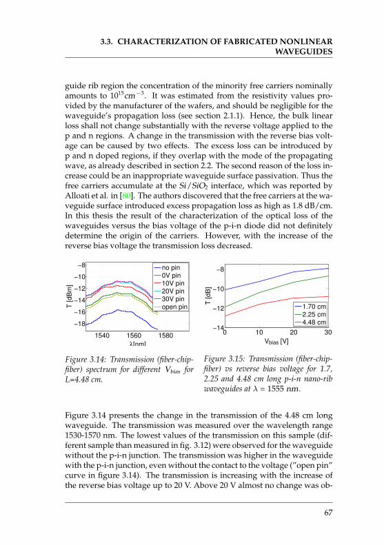
3.3. CHARACTERIZATION OF FABRICATED NONLINEARWAVEGUIDES
guide rib region the concentration of the minority free carriers nominallyamounts to 1015cm−3. It was estimated from the resistivity values pro-vided by the manufacturer of the wafers, and should be negligible for thewaveguide’s propagation loss (see section 2.1.1). Hence, the bulk linearloss shall not change substantially with the reverse voltage applied to thep and n regions. A change in the transmission with the reverse bias volt-age can be caused by two effects. The excess loss can be introduced byp and n doped regions, if they overlap with the mode of the propagatingwave, as already described in section 2.2. The second reason of the loss in-crease could be an inappropriate waveguide surface passivation. Thus thefree carriers accumulate at the Si/SiO2 interface, which was reported byAlloati et al. in [80]. The authors discovered that the free carriers at the wa-veguide surface introduced excess propagation loss as high as 1.8 dB/cm.In this thesis the result of the characterization of the optical loss of thewaveguides versus the bias voltage of the p-i-n diode did not definitelydetermine the origin of the carriers. However, with the increase of thereverse bias voltage the transmission loss decreased.
1540 1560 1580
−18
−16
−14
−12
−10
−8
λ[nm]
T [dB
m]
no pin0V pin10V pin20V pin30V pinopen pin
Figure 3.14: Transmission (fiber-chip-fiber) spectrum for different Vbias forL=4.48 cm.
0 10 20 30−14
−12
−10
−8
Vbias [V]
T [dB
]
1.70 cm2.25 cm4.48 cm
Figure 3.15: Transmission (fiber-chip-fiber) vs reverse bias voltage for 1.7,2.25 and 4.48 cm long p-i-n nano-ribwaveguides at λ = 1555 nm .
Figure 3.14 presents the change in the transmission of the 4.48 cm longwaveguide. The transmission was measured over the wavelength range1530-1570 nm. The lowest values of the transmission on this sample (dif-ferent sample than measured in fig. 3.12) were observed for the waveguidewithout the p-i-n junction. The transmission was higher in the waveguidewith the p-i-n junction, even without the contact to the voltage (”open pin”curve in figure 3.14). The transmission is increasing with the increase ofthe reverse bias voltage up to 20 V. Above 20 V almost no change was ob-
67
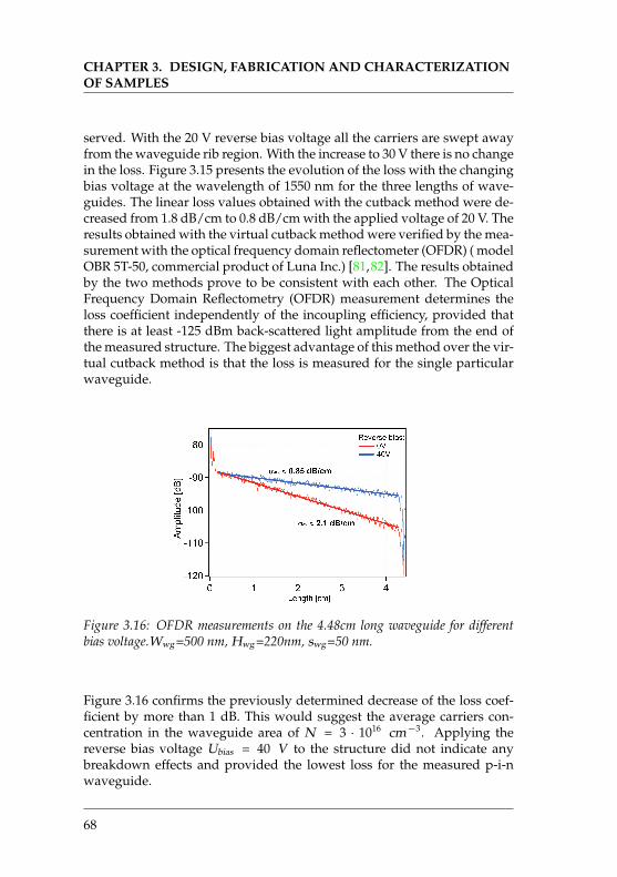
CHAPTER 3. DESIGN, FABRICATION AND CHARACTERIZATIONOF SAMPLES
served. With the 20 V reverse bias voltage all the carriers are swept awayfrom the waveguide rib region. With the increase to 30 V there is no changein the loss. Figure 3.15 presents the evolution of the loss with the changingbias voltage at the wavelength of 1550 nm for the three lengths of wave-guides. The linear loss values obtained with the cutback method were de-creased from 1.8 dB/cm to 0.8 dB/cm with the applied voltage of 20 V. Theresults obtained with the virtual cutback method were verified by the mea-surement with the optical frequency domain reflectometer (OFDR) ( modelOBR 5T-50, commercial product of Luna Inc.) [81,82]. The results obtainedby the two methods prove to be consistent with each other. The OpticalFrequency Domain Reflectometry (OFDR) measurement determines theloss coefficient independently of the incoupling efficiency, provided thatthere is at least -125 dBm back-scattered light amplitude from the end ofthe measured structure. The biggest advantage of this method over the vir-tual cutback method is that the loss is measured for the single particularwaveguide.
Figure 3.16: OFDR measurements on the 4.48cm long waveguide for differentbias voltage.Wwg =500 nm, Hwg =220nm, swg =50 nm.
Figure 3.16 confirms the previously determined decrease of the loss coef-ficient by more than 1 dB. This would suggest the average carriers con-centration in the waveguide area of N = 3 · 1016 cm−3. Applying thereverse bias voltage Ubias = 40 V to the structure did not indicate anybreakdown effects and provided the lowest loss for the measured p-i-nwaveguide.
68
3.3. CHARACTERIZATION OF FABRICATED NONLINEARWAVEGUIDES
3.3.5 Power dependent loss due to TPA and FCA
The power dependent loss in a silicon waveguide at the wavelengtharound 1550 nm originates from the two photon absorption (TPA) andthe TPA induced free carrier absorption (FCA). Both absorption mech-anisms have the detrimental impact on the nonlinear optical effects in asilicon waveguide. Therefore, their influence needs to be tested, quantifiedand minimized. The impact of the FCA effect can be treated as negligibleuntil a certain power level. The results reported later in this section showthese limits.
The experimental results discussed later leading to the determination ofthe βTPA were provided by Edgar Krune (TUB). To quantify the TPA highpeak power optical pulses were incoupled to the shallow etched wave-guides with the length Lwg = 1 cm , 3 cm and 6 cm . The waveguide widthwas Wwg = 700 nm , the height equals Hwg = 220 nm and the slab thick-ness amounted to swg = 150 nm . The effective area Aeff = 0.14 µm2, cal-culated with the JCMWave software, and the measured linear loss αlin =0.88 dB/cm , were used in the calculations. Here the methodology appliedto the measurement and the result evaluation followed the methodologyof Claps et al. [83]. It was assured that the conditions were similar to thoseused by Claps et al. (e.g. pulses not longer than 1 ps , low repetition rateand optical intensity). To determine the TPA coefficient (βTPA ) the follow-ing formula was used (as in equation (1.37)):
P peak (0)P peak (Lwg )
= eαlin Lwg
(1 +
βTPA Leff
AeffP peak (0)
)(3.2)
hence:
βTPA = − c1Aeff
Leffe−αlin Lwg (3.3)
where Aeff represents the effective nonlinear area as defined in section 1.2.5and Leff = ((1− exp(−αlin Lwg ))/αlin ) is the effective length. The coefficientc1 is the slope of the curve P peak (0)/P peak (Lwg ) versus P (0)peak , plotted infigure 3.18. The linear loss coefficient αlin was measured in this case by thevirtual cutback method, and Lwg is the physical waveguide length.
The measurement setup depicted in figure 3.17 was used to determine theTPA coefficient βTPA . During the measurement the pulse of 80 fs was gen-erated by a mode-locked laser with the repetition rate of 100 MHz. The
69
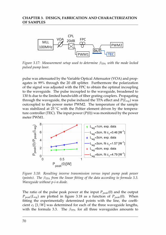
CHAPTER 3. DESIGN, FABRICATION AND CHARACTERIZATIONOF SAMPLES
PWM2
DUT
FPC
DUT
TEC
CPL
20dBVOA
MLL
100MHz
PWM1
Figure 3.17: Measurement setup used to determine βTPA with the mode lockedpulsed pump laser.
pulse was attenuated by the Variable Optical Attenuator (VOA) and prop-agates in 99% through the 20 dB splitter. Furthermore the polarizationof the signal was adjusted with the FPC to obtain the optimal incouplingto the waveguide. The pulse incoupled to the waveguide, broadened to130 fs due to the limited bandwidth of fiber grating couplers. Propagatingthrough the waveguide, the pulse induced the TPA effect and P (Lwg ) wasoutcoupled to the power meter PWM2. The temperature of the samplewas stabilized at 25 ◦C with the Peltier element driven by the tempera-ture controller (TEC). The input power (P (0)) was monitored by the powermeter PWM1.
0 0.5 1
Ppeak
(0)[W]
0
2
4
6
8
Ppeak(0
)/P
peak(L
wg)
Lwg
=1cm, exp. data
Lwg
=3cm, fit c1=0.46 [W-1]
Lwg
=3cm, exp. data
Lwg
=3cm, fit c1=1.57 [W-1]
Lwg
=6cm, exp. data
Lwg
=6cm, fit c1=4.79 [W-1]
Figure 3.18: Resulting inverse transmission versus input pump peak power(points). The βTPA from the linear fitting of the data according to formula 3.3.Waveguide without p-i-n diode.
The ratio of the pulse peak power at the input P peak (0) and the outputP peak (Lwg ) are plotted in figure 3.18 as a function of P peak (0). Whenfitting the experimentally determined points with the line, the coeffi-cient c1 [1/W ] was determined for each of the three waveguide lengths,with the formula 3.3. The βTPA for all three waveguides amounts to
70
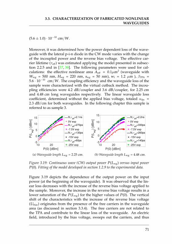
3.3. CHARACTERIZATION OF FABRICATED NONLINEARWAVEGUIDES
(5.6 ± 1.0) · 10−10 cm/W .
Moreover, it was determined how the power dependent loss of the wave-guide with the lateral p-i-n diode in the CW mode varies with the changeof the incoupled power and the reverse bias voltage. The effective car-rier lifetime (τeff ) was estimated applying the model presented in subsec-tion 2.2.5 and in [37, 38]. The following parameters were used for cal-culations: the effective nonlinear area Aeff = 0.1µm2 (waveguide withWwg = 500 nm , Hwg = 220 nm , swg = 50 nm), wi = 1.2 µm ), βTPA =5.6 · 10−10 cm/W . The coupling efficiency and the waveguide loss of thesample were characterized with the virtual cutback method. The incou-pling efficiencies were 4.2 dB/coupler and 3.6 dB/coupler, for 2.25 cmand 4.48 cm long waveguides respectively. The linear waveguide losscoefficient, determined without the applied bias voltage, totaled αlin =2.3 dB/cm for both waveguides. In the following chapter this sample isreferred to as sample 3.
10 20
P(0) [dBm]
-5
0
5
10
15
P(L
wg)
[dB
m]
fit,eff
=2.1ns
0V exp
fit,eff
=270ps
-7.5V exp
fit,eff
=130ps
-15V exp
fit,eff
=60ps
-25V exp
(a) Waveguide length Lwg = 2.25 cm .
10 20
P(0) [dBm]
-5
0
5
10
15
P(L
wg)
[dB
m]
fit,eff
=2.2ns
0V exp
fit,eff
=330ps
-7.5V exp
fit,eff
=260ps
-15V exp
fit,eff
=140ps
-25V exp
(b) Waveguide length Lwg = 4.48 cm .
Figure 3.19: Continuous wave (CW) output power P (Lwg ) versus input powerP (0). Fitting of the model developed in section 1.2.9 to the experimental data.
Figure 3.19 depicts the dependence of the output power on the inputpower (at the beginning of the waveguide). It was observed that the lin-ear loss decreases with the increase of the reverse bias voltage applied tothe sample. Moreover, the increase in the reverse bias voltage results in alower saturation of the P (Lwg ) for the higher values of P (0). The verticalshift of the characteristics with the increase of the reverse bias voltage(Ubias ) originates from the presence of the free carriers in the waveguidearea (as discussed in section 3.3.4). The free carriers are not related tothe TPA and contribute to the linear loss of the waveguide. An electricfield, introduced by the bias voltage, sweeps out the carriers, and thus
71
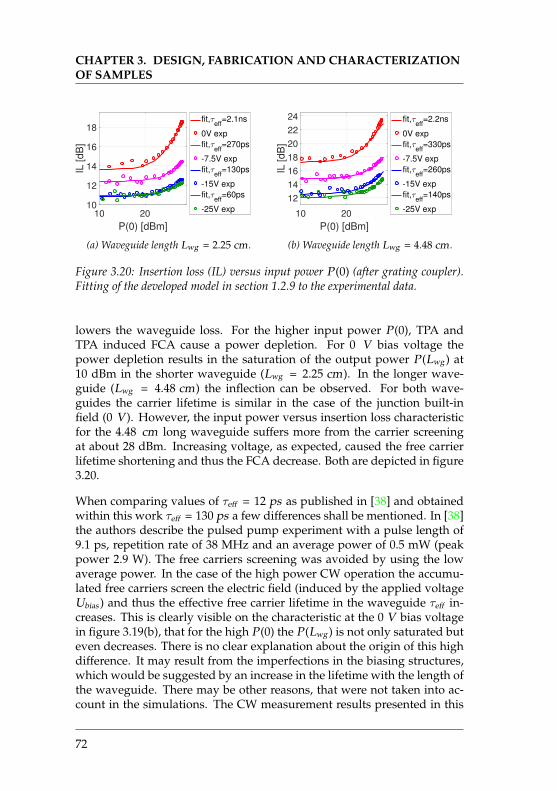
CHAPTER 3. DESIGN, FABRICATION AND CHARACTERIZATIONOF SAMPLES
10 20
P(0) [dBm]
10
12
14
16
18
IL [
dB
]
fit,eff
=2.1ns
0V exp
fit,eff
=270ps
-7.5V exp
fit,eff
=130ps
-15V exp
fit,eff
=60ps
-25V exp
(a) Waveguide length Lwg = 2.25 cm .
10 20
P(0) [dBm]
12
14
16
18
20
22
24
IL [
dB
]
fit,eff
=2.2ns
0V exp
fit,eff
=330ps
-7.5V exp
fit,eff
=260ps
-15V exp
fit,eff
=140ps
-25V exp
(b) Waveguide length Lwg = 4.48 cm .
Figure 3.20: Insertion loss (IL) versus input power P (0) (after grating coupler).Fitting of the developed model in section 1.2.9 to the experimental data.
lowers the waveguide loss. For the higher input power P (0), TPA andTPA induced FCA cause a power depletion. For 0 V bias voltage thepower depletion results in the saturation of the output power P (Lwg ) at10 dBm in the shorter waveguide (Lwg = 2.25 cm). In the longer wave-guide (Lwg = 4.48 cm) the inflection can be observed. For both wave-guides the carrier lifetime is similar in the case of the junction built-infield (0 V ). However, the input power versus insertion loss characteristicfor the 4.48 cm long waveguide suffers more from the carrier screeningat about 28 dBm. Increasing voltage, as expected, caused the free carrierlifetime shortening and thus the FCA decrease. Both are depicted in figure3.20.
When comparing values of τeff = 12 ps as published in [38] and obtainedwithin this work τeff = 130 ps a few differences shall be mentioned. In [38]the authors describe the pulsed pump experiment with a pulse length of9.1 ps, repetition rate of 38 MHz and an average power of 0.5 mW (peakpower 2.9 W). The free carriers screening was avoided by using the lowaverage power. In the case of the high power CW operation the accumu-lated free carriers screen the electric field (induced by the applied voltageUbias ) and thus the effective free carrier lifetime in the waveguide τeff in-creases. This is clearly visible on the characteristic at the 0 V bias voltagein figure 3.19(b), that for the high P (0) the P (Lwg ) is not only saturated buteven decreases. There is no clear explanation about the origin of this highdifference. It may result from the imperfections in the biasing structures,which would be suggested by an increase in the lifetime with the length ofthe waveguide. There may be other reasons, that were not taken into ac-count in the simulations. The CW measurement results presented in this
72
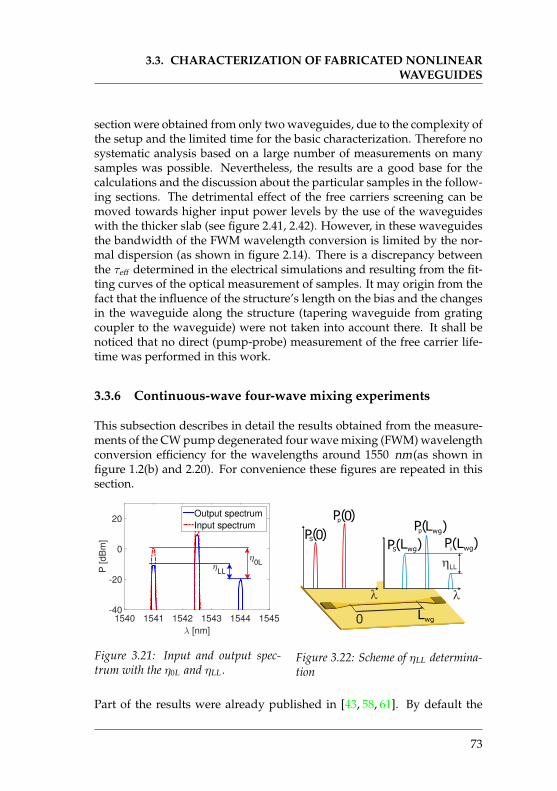
3.3. CHARACTERIZATION OF FABRICATED NONLINEARWAVEGUIDES
section were obtained from only two waveguides, due to the complexity ofthe setup and the limited time for the basic characterization. Therefore nosystematic analysis based on a large number of measurements on manysamples was possible. Nevertheless, the results are a good base for thecalculations and the discussion about the particular samples in the follow-ing sections. The detrimental effect of the free carriers screening can bemoved towards higher input power levels by the use of the waveguideswith the thicker slab (see figure 2.41, 2.42). However, in these waveguidesthe bandwidth of the FWM wavelength conversion is limited by the nor-mal dispersion (as shown in figure 2.14). There is a discrepancy betweenthe τeff determined in the electrical simulations and resulting from the fit-ting curves of the optical measurement of samples. It may origin from thefact that the influence of the structure’s length on the bias and the changesin the waveguide along the structure (tapering waveguide from gratingcoupler to the waveguide) were not taken into account there. It shall benoticed that no direct (pump-probe) measurement of the free carrier life-time was performed in this work.
3.3.6 Continuous-wave four-wave mixing experiments
This subsection describes in detail the results obtained from the measure-ments of the CW pump degenerated four wave mixing (FWM) wavelengthconversion efficiency for the wavelengths around 1550 nm(as shown infigure 1.2(b) and 2.20). For convenience these figures are repeated in thissection.
λ [nm]
1540 1541 1542 1543 1544 1545
P [
dB
m]
-40
-20
0
20Output spectrum
Input spectrum
ηLL
η0L
Figure 3.21: Input and output spec-trum with the η0L and ηLL .
Pp )(0
LwgPi
Lwg
)(LwgPS )()0PS(
Pp(Lwg)
Figure 3.22: Scheme of ηLL determina-tion
Part of the results were already published in [43, 58, 61]. By default the
73
CHAPTER 3. DESIGN, FABRICATION AND CHARACTERIZATIONOF SAMPLES
beginning of the waveguide is defined in the position 0 and the end ofthe waveguide in the position Lwg , as depicted in figure 3.22. This is thecase unless the contrary is explicitly mentioned. Furthermore, the depen-dence of the wavelength conversion on the following factors was exam-ined:
• the waveguide length Lwg ,
• the presence of the lateral p-i-n diode,
• the detuning of the signal from the pump wavelength (∆λ),
• the reverse bias voltage applied (Ubias ),
• and the incoupled pump power at the beginning of the waveguide(Pp (0)).
For this purpose two setups were built and several experiments were per-formed. Three samples were fabricated in the same production process.They had the same design and were constructed on the same type of SOIwafer. These samples were used in the experiments. It must be noted thatthe samples are not identical. There may be differences in their propertiessuch as: waveguide loss, incoupling efficiency and the maximum reversebias voltage. These differences may originate from the deviation in thefabrication process steps. In the first experiment session the samples 1and 2 were used. The sample 3 was subject to the second measurementsession. Samples 1 and 3 originate from the same wafer, whereas the sam-ple 2 comes from the another wafer. Each sample contains waveguideswith and without lateral p-i-n junction. The first results were obtained bymeasuring the waveguides with and without the lateral p-i-n junction onsample 1. Some of the grating couplers experienced a spot burning whenexposed to the high intensity laser beam (106 W/cm2). Therefore, for thenext measurements sample 2 was used. The problem of the spot burningappeared firstly, due to a short, high power pulses generated by an ErbiumDoped Fiber Amplifier (EDFA) during the electrical tuning of the outputpower. The other reason was dust or defects laying over or on the top ofthe grating coupler area.
The setup of the first measurement is presented in figure 3.23. Two tunablelaser sources (TLS ) were used. The first TLS emitted the signal light andwas connected to one arm of the Fiber Optic Coupler (CPL)1. The lightfrom the second TLS was amplified by EDFA (marked as pump laser infigure 3.23). The power of the pump was tuned with the mechanical vari-able optical attenuator (VOA). The pump laser was attached to the second
74
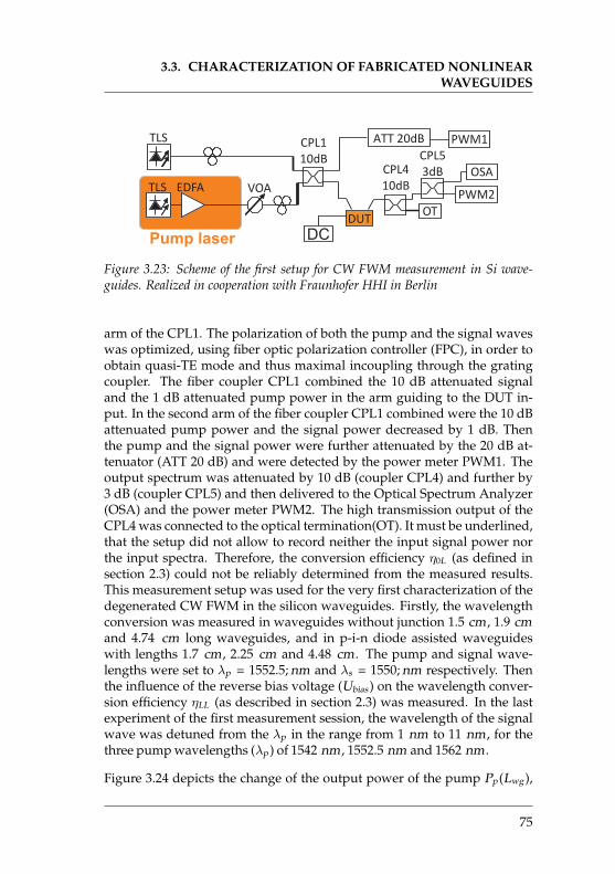
3.3. CHARACTERIZATION OF FABRICATED NONLINEARWAVEGUIDES
TLS
EDFA VOA
DUT
TLS
Pump laser
CPL1
10dB
ATT 20dB PWM1
DC
OSA
CPL5
3dB
PWM2
CPL4
10dB
OT
Figure 3.23: Scheme of the first setup for CW FWM measurement in Si wave-guides. Realized in cooperation with Fraunhofer HHI in Berlin
arm of the CPL1. The polarization of both the pump and the signal waveswas optimized, using fiber optic polarization controller (FPC), in order toobtain quasi-TE mode and thus maximal incoupling through the gratingcoupler. The fiber coupler CPL1 combined the 10 dB attenuated signaland the 1 dB attenuated pump power in the arm guiding to the DUT in-put. In the second arm of the fiber coupler CPL1 combined were the 10 dBattenuated pump power and the signal power decreased by 1 dB. Thenthe pump and the signal power were further attenuated by the 20 dB at-tenuator (ATT 20 dB) and were detected by the power meter PWM1. Theoutput spectrum was attenuated by 10 dB (coupler CPL4) and further by3 dB (coupler CPL5) and then delivered to the Optical Spectrum Analyzer(OSA) and the power meter PWM2. The high transmission output of theCPL4 was connected to the optical termination(OT). It must be underlined,that the setup did not allow to record neither the input signal power northe input spectra. Therefore, the conversion efficiency η0L (as defined insection 2.3) could not be reliably determined from the measured results.This measurement setup was used for the very first characterization of thedegenerated CW FWM in the silicon waveguides. Firstly, the wavelengthconversion was measured in waveguides without junction 1.5 cm , 1.9 cmand 4.74 cm long waveguides, and in p-i-n diode assisted waveguideswith lengths 1.7 cm , 2.25 cm and 4.48 cm . The pump and signal wave-lengths were set to λp = 1552.5; nm and λs = 1550; nm respectively. Thenthe influence of the reverse bias voltage (Ubias ) on the wavelength conver-sion efficiency ηLL (as described in section 2.3) was measured. In the lastexperiment of the first measurement session, the wavelength of the signalwave was detuned from the λp in the range from 1 nm to 11 nm , for thethree pump wavelengths (λp ) of 1542 nm , 1552.5 nm and 1562 nm .
Figure 3.24 depicts the change of the output power of the pump Pp (Lwg ),
75
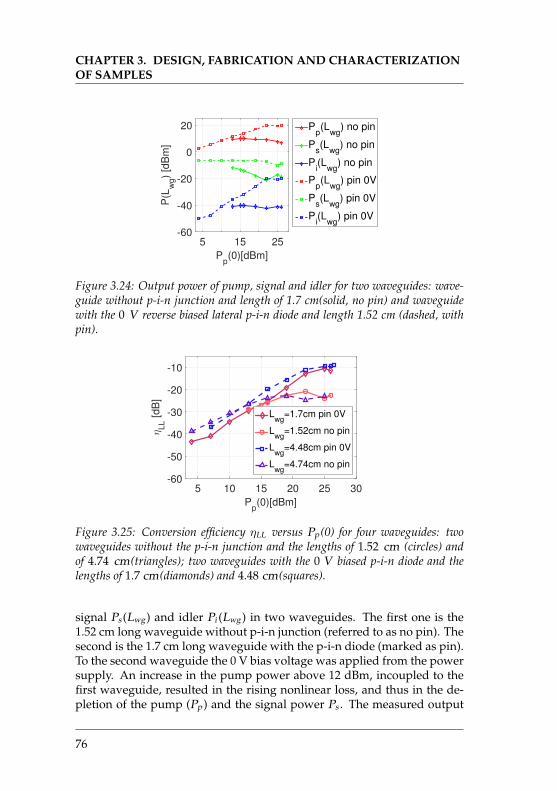
CHAPTER 3. DESIGN, FABRICATION AND CHARACTERIZATIONOF SAMPLES
Pp(0)[dBm]
5 15 25
P(L
wg)
[dB
m]
-60
-40
-20
0
20 Pp(L
wg) no pin
Ps(L
wg) no pin
Pi(L
wg) no pin
Pp(L
wg) pin 0V
Ps(L
wg) pin 0V
Pi(L
wg) pin 0V
Figure 3.24: Output power of pump, signal and idler for two waveguides: wave-guide without p-i-n junction and length of 1.7 cm(solid, no pin) and waveguidewith the 0 V reverse biased lateral p-i-n diode and length 1.52 cm (dashed, withpin).
Pp(0)[dBm]
5 10 15 20 25 30
ηL
L [
dB
]
-60
-50
-40
-30
-20
-10
Lwg
=1.7cm pin 0V
Lwg
=1.52cm no pin
Lwg
=4.48cm pin 0V
Lwg
=4.74cm no pin
Figure 3.25: Conversion efficiency ηLL versus Pp (0) for four waveguides: twowaveguides without the p-i-n junction and the lengths of 1.52 cm (circles) andof 4.74 cm(triangles); two waveguides with the 0 V biased p-i-n diode and thelengths of 1.7 cm(diamonds) and 4.48 cm(squares).
signal Ps (Lwg ) and idler Pi (Lwg ) in two waveguides. The first one is the1.52 cm long waveguide without p-i-n junction (referred to as no pin). Thesecond is the 1.7 cm long waveguide with the p-i-n diode (marked as pin).To the second waveguide the 0 V bias voltage was applied from the powersupply. An increase in the pump power above 12 dBm, incoupled to thefirst waveguide, resulted in the rising nonlinear loss, and thus in the de-pletion of the pump (Pp ) and the signal power Ps . The measured output
76
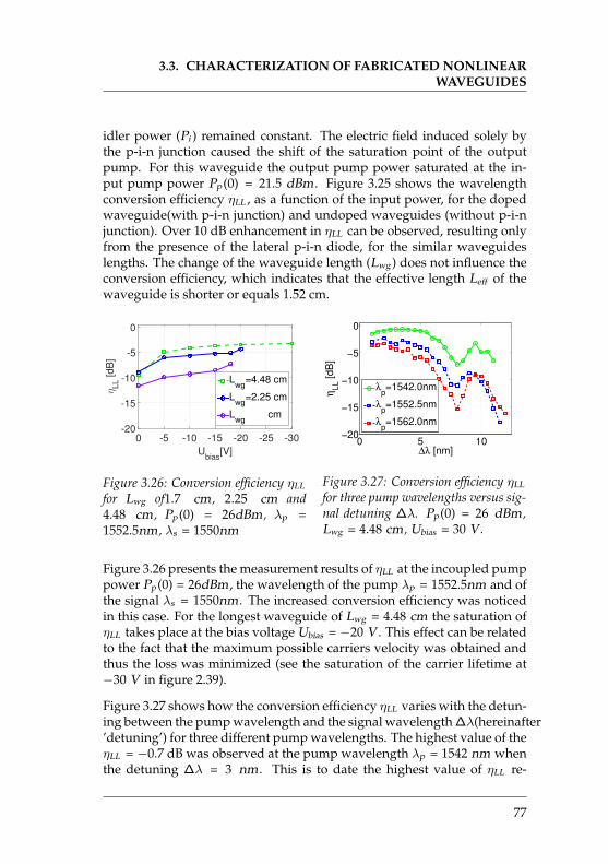
3.3. CHARACTERIZATION OF FABRICATED NONLINEARWAVEGUIDES
idler power (Pi ) remained constant. The electric field induced solely bythe p-i-n junction caused the shift of the saturation point of the outputpump. For this waveguide the output pump power saturated at the in-put pump power Pp (0) = 21.5 dBm . Figure 3.25 shows the wavelengthconversion efficiency ηLL , as a function of the input power, for the dopedwaveguide(with p-i-n junction) and undoped waveguides (without p-i-njunction). Over 10 dB enhancement in ηLL can be observed, resulting onlyfrom the presence of the lateral p-i-n diode, for the similar waveguideslengths. The change of the waveguide length (Lwg ) does not influence theconversion efficiency, which indicates that the effective length Leff of thewaveguide is shorter or equals 1.52 cm.
Ubias
[V]
0 -5 -10 -15 -20 -25 -30
ηLL [
dB
]
-20
-15
-10
-5
0
Lwg
=4.48 cm
Lwg
=2.25 cm
Lwg
cm
Figure 3.26: Conversion efficiency ηLL
for Lwg of1.7 cm , 2.25 cm and4.48 cm , Pp (0) = 26dBm , λp =1552.5nm , λs = 1550nm
0 5 10−20
−15
−10
−5
0
∆λ [nm]
ηLL [dB
]
λp=1542.0nm
λp=1552.5nm
λp=1562.0nm
Figure 3.27: Conversion efficiency ηLL
for three pump wavelengths versus sig-nal detuning ∆λ. Pp (0) = 26 dBm ,Lwg = 4.48 cm , Ubias = 30 V .
Figure 3.26 presents the measurement results of ηLL at the incoupled pumppower Pp (0) = 26dBm , the wavelength of the pump λp = 1552.5nm and ofthe signal λs = 1550nm . The increased conversion efficiency was noticedin this case. For the longest waveguide of Lwg = 4.48 cm the saturation ofηLL takes place at the bias voltage Ubias = −20 V . This effect can be relatedto the fact that the maximum possible carriers velocity was obtained andthus the loss was minimized (see the saturation of the carrier lifetime at−30 V in figure 2.39).
Figure 3.27 shows how the conversion efficiency ηLL varies with the detun-ing between the pump wavelength and the signal wavelength ∆λ(hereinafter’detuning’) for three different pump wavelengths. The highest value of theηLL = −0.7 dB was observed at the pump wavelength λp = 1542 nm whenthe detuning ∆λ = 3 nm . This is to date the highest value of ηLL re-
77
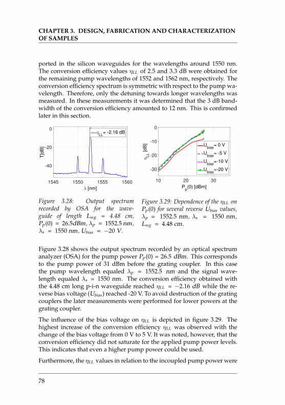
CHAPTER 3. DESIGN, FABRICATION AND CHARACTERIZATIONOF SAMPLES
ported in the silicon waveguides for the wavelengths around 1550 nm.The conversion efficiency values ηLL of 2.5 and 3.3 dB were obtained forthe remaining pump wavelengths of 1552 and 1562 nm, respectively. Theconversion efficiency spectrum is symmetric with respect to the pump wa-velength. Therefore, only the detuning towards longer wavelengths wasmeasured. In these measurements it was determined that the 3 dB band-width of the conversion efficiency amounted to 12 nm. This is confirmedlater in this section.
λ [nm]
1545 1550 1555 1560
T[d
B]
-40
-20
0η
LL= -2.16 dB
Figure 3.28: Output spectrumrecorded by OSA for the wave-guide of length Lwg = 4.48 cm,Pp (0) = 26.5dBm , λp = 1552.5 nm ,λs = 1550 nm , Ubias = −20 V .
Pp(0) [dBm]
10 20 30
ηLL [
dB
]
-30
-20
-10
0
Ubias
= 0 V
Ubias
= -5 V
Ubias
=-10 V
Ubias
=-20 V
Figure 3.29: Dependence of the ηLL onPp (0) for several reverse Ubias values,λp = 1552.5 nm , λs = 1550 nm ,Lwg = 4.48 cm .
Figure 3.28 shows the output spectrum recorded by an optical spectrumanalyzer (OSA) for the pump power Pp (0) = 26.5 dBm . This correspondsto the pump power of 31 dBm before the grating coupler. In this casethe pump wavelength equaled λp = 1552.5 nm and the signal wave-length equaled λs = 1550 nm . The conversion efficiency obtained withthe 4.48 cm long p-i-n waveguide reached ηLL = −2.16 dB while the re-verse bias voltage (Ubias ) reached -20 V. To avoid destruction of the gratingcouplers the later measurements were performed for lower powers at thegrating coupler.
The influence of the bias voltage on ηLL is depicted in figure 3.29. Thehighest increase of the conversion efficiency ηLL was observed with thechange of the bias voltage from 0 V to 5 V. It was noted, however, that theconversion efficiency did not saturate for the applied pump power levels.This indicates that even a higher pump power could be used.
Furthermore, the ηLL values in relation to the incoupled pump power were
78
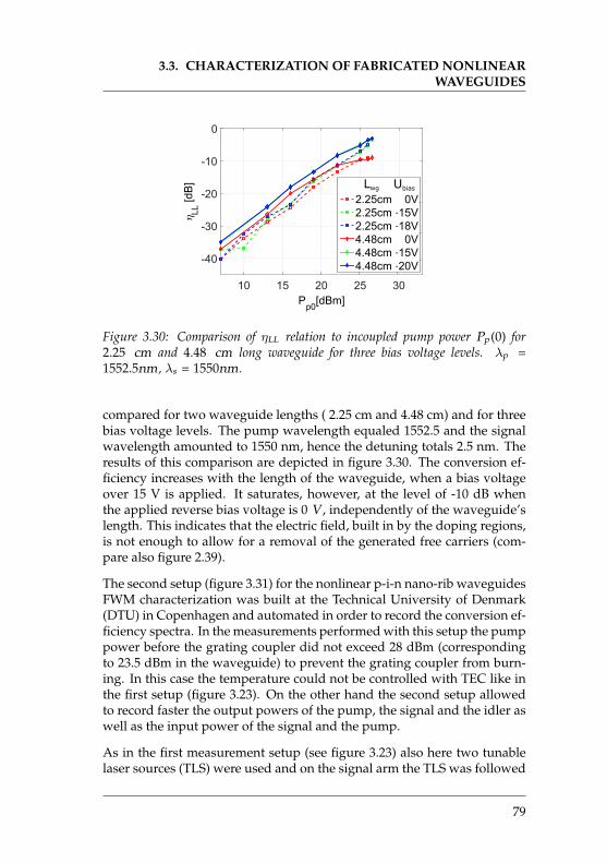
3.3. CHARACTERIZATION OF FABRICATED NONLINEARWAVEGUIDES
Lwg Ubias
-
-
-
-
Figure 3.30: Comparison of ηLL relation to incoupled pump power Pp (0) for2.25 cm and 4.48 cm long waveguide for three bias voltage levels. λp =1552.5nm , λs = 1550nm .
compared for two waveguide lengths ( 2.25 cm and 4.48 cm) and for threebias voltage levels. The pump wavelength equaled 1552.5 and the signalwavelength amounted to 1550 nm, hence the detuning totals 2.5 nm. Theresults of this comparison are depicted in figure 3.30. The conversion ef-ficiency increases with the length of the waveguide, when a bias voltageover 15 V is applied. It saturates, however, at the level of -10 dB whenthe applied reverse bias voltage is 0 V , independently of the waveguide’slength. This indicates that the electric field, built in by the doping regions,is not enough to allow for a removal of the generated free carriers (com-pare also figure 2.39).
The second setup (figure 3.31) for the nonlinear p-i-n nano-rib waveguidesFWM characterization was built at the Technical University of Denmark(DTU) in Copenhagen and automated in order to record the conversion ef-ficiency spectra. In the measurements performed with this setup the pumppower before the grating coupler did not exceed 28 dBm (correspondingto 23.5 dBm in the waveguide) to prevent the grating coupler from burn-ing. In this case the temperature could not be controlled with TEC like inthe first setup (figure 3.23). On the other hand the second setup allowedto record faster the output powers of the pump, the signal and the idler aswell as the input power of the signal and the pump.
As in the first measurement setup (see figure 3.23) also here two tunablelaser sources (TLS) were used and on the signal arm the TLS was followed
79
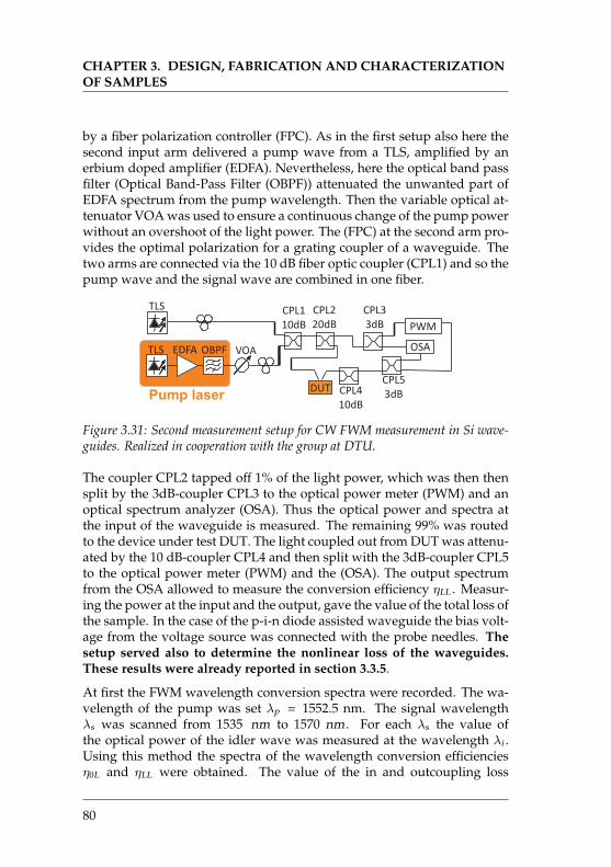
CHAPTER 3. DESIGN, FABRICATION AND CHARACTERIZATIONOF SAMPLES
by a fiber polarization controller (FPC). As in the first setup also here thesecond input arm delivered a pump wave from a TLS, amplified by anerbium doped amplifier (EDFA). Nevertheless, here the optical band passfilter (Optical Band-Pass Filter (OBPF)) attenuated the unwanted part ofEDFA spectrum from the pump wavelength. Then the variable optical at-tenuator VOA was used to ensure a continuous change of the pump powerwithout an overshoot of the light power. The (FPC) at the second arm pro-vides the optimal polarization for a grating coupler of a waveguide. Thetwo arms are connected via the 10 dB fiber optic coupler (CPL1) and so thepump wave and the signal wave are combined in one fiber.
TLS
EDFA OBPF VOA
PWM
OSATLS
Pump laser
CPL1
10dB
CPL2
20dB
CPL3
3dB
DUT CPL4
10dB
CPL5
3dB
Figure 3.31: Second measurement setup for CW FWM measurement in Si wave-guides. Realized in cooperation with the group at DTU.
The coupler CPL2 tapped off 1% of the light power, which was then thensplit by the 3dB-coupler CPL3 to the optical power meter (PWM) and anoptical spectrum analyzer (OSA). Thus the optical power and spectra atthe input of the waveguide is measured. The remaining 99% was routedto the device under test DUT. The light coupled out from DUT was attenu-ated by the 10 dB-coupler CPL4 and then split with the 3dB-coupler CPL5to the optical power meter (PWM) and the (OSA). The output spectrumfrom the OSA allowed to measure the conversion efficiency ηLL . Measur-ing the power at the input and the output, gave the value of the total loss ofthe sample. In the case of the p-i-n diode assisted waveguide the bias volt-age from the voltage source was connected with the probe needles. Thesetup served also to determine the nonlinear loss of the waveguides.These results were already reported in section 3.3.5.
At first the FWM wavelength conversion spectra were recorded. The wa-velength of the pump was set λp = 1552.5 nm. The signal wavelengthλs was scanned from 1535 nm to 1570 nm . For each λs the value ofthe optical power of the idler wave was measured at the wavelength λi .Using this method the spectra of the wavelength conversion efficienciesη0L and ηLL were obtained. The value of the in and outcoupling loss
80
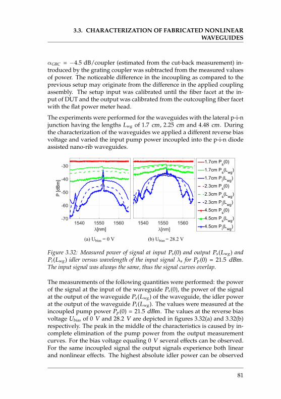
3.3. CHARACTERIZATION OF FABRICATED NONLINEARWAVEGUIDES
αGRC = −4.5 dB/coupler (estimated from the cut-back measurement) in-troduced by the grating coupler was subtracted from the measured valuesof power. The noticeable difference in the incoupling as compared to theprevious setup may originate from the difference in the applied couplingassembly. The setup input was calibrated until the fiber facet at the in-put of DUT and the output was calibrated from the outcoupling fiber facetwith the flat power meter head.
The experiments were performed for the waveguides with the lateral p-i-njunction having the lengths Lwg of 1.7 cm , 2.25 cm and 4.48 cm . Duringthe characterization of the waveguides we applied a different reverse biasvoltage and varied the input pump power incoupled into the p-i-n diodeassisted nano-rib waveguides.
(a) Ubias = 0 V (b) Ubias = 28.2 V
Figure 3.32: Measured power of signal at input Ps (0) and output Ps (Lwg ) andPi (Lwg ) idler versus wavelength of the input signal λs for Pp (0) = 21.5 dBm .The input signal was always the same, thus the signal curves overlap.
The measurements of the following quantities were performed: the powerof the signal at the input of the waveguide Ps (0), the power of the signalat the output of the waveguide Ps (Lwg ) of the waveguide, the idler powerat the output of the waveguide Pi (Lwg ). The values were measured at theincoupled pump power Pp (0) = 21.5 dBm . The values at the reverse biasvoltage Ubias of 0 V and 28.2 V are depicted in figures 3.32(a) and 3.32(b)respectively. The peak in the middle of the characteristics is caused by in-complete elimination of the pump power from the output measurementcurves. For the bias voltage equaling 0 V several effects can be observed.For the same incoupled signal the output signals experience both linearand nonlinear effects. The highest absolute idler power can be observed
81
CHAPTER 3. DESIGN, FABRICATION AND CHARACTERIZATIONOF SAMPLES
for the shortest waveguide. For the the longer waveguides the idler powerdecreases. However, the distance between the green (power of the signalat the output) and the corresponding blue curve remains the same for eachwaveguide. This results in the same ηLL for all lengths, while the highestvalue of η0L was observed for the 1.7 cm long waveguide. Increasing thelength of the waveguide Lwg diminishes the bandwidth of the wavelengthconversion. It results from the fact that all three waveguides have a highnormal dispersion due to their dimensions Wwg = 500 nm , Hwg = 220 nmand swg = 50 nm . At the bias voltage of 0 V the shortest waveguide wouldbe the best choice for the wavelength conversion’s point of view. It is dueto the highest conversion efficiency η0L and the widest conversion effi-ciency bandwidth (BW ).
However, the reverse biasing of the p-i-n diode with the 28.2 V volt-age changes a situation. The longest waveguide (Lwg = 4.48 cm) emit-ted 1 dB more maximal idler power than the shortest waveguide (Lwg =1.7 cm). Despite the highest idler power obtained in the 4.48 cm longwaveguide, the disadvantageous narrow bandwidth remains. The resultshows that for the normal dispersion the FWM wavelength conversion ef-ficiency bandwidth becomes narrower with the increase of the waveguidelength. This situation would be even more disadvantageous in case of theshallow etched waveguides with the very low loss [52], since they haveeven higher normal dispersion. The very low loss of these waveguideswould predestine them for the nonlinear optical applications. Neverthe-less, their high normal dispersion and an effective area Aeff = 0.14 µm2,would limit the bandwidth and the FWM based wavelength conversionefficiency.
Figure 3.33 depicts the measured values of the ηLL (ratio of the output idlerpower to output signal power) and the η0L (ratio of the output idler powerto input signal power) for the pump power Pp (0) = 21.5 dBm . The mea-sured conversion efficiency is presented as the function of the wavelengthof the input signal λs . The measurements were conducted for the wave-guide lengths of 1.7 cm, 2.25 cm and 4.48 cm, whereas the bias voltagewas 0 V. For the shortest and the longest waveguides similar values of ηLL
were obtained. The η0L (eq. (2.8)), however, shows the loss contributionof the waveguide. Therefore, the highest conversion efficiency η0L was ob-tained for the 1.7 cm long waveguide. Applying the 28.2 V bias voltage,the conversion efficiency values (both η0L and ηLL ) became the highest inthe longest waveguide. The optical loss due to the free carriers decreased,which led to an enhancement in η0L by 3.2, 8.9 and 12.6 dB while ηLL was
82
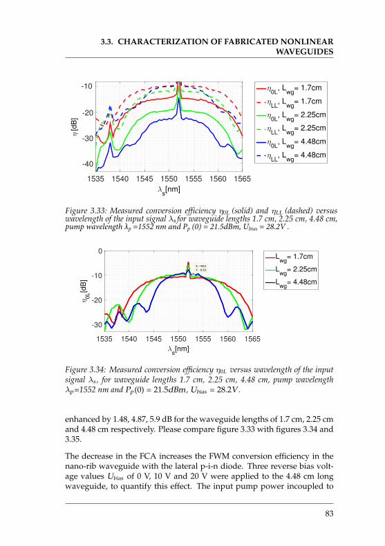
3.3. CHARACTERIZATION OF FABRICATED NONLINEARWAVEGUIDES
λs[nm]
1535 1540 1545 1550 1555 1560 1565
-40
-30
-20
-10 η0L
, Lwg
= 1.7cm
ηLL
, Lwg
= 1.7cm
η0L
, Lwg
= 2.25cm
ηLL
, Lwg
= 2.25cm
η0L
, Lwg
= 4.48cm
ηLL
, Lwg
= 4.48cm
Figure 3.33: Measured conversion efficiency η0L (solid) and ηLL (dashed) versus wavelength of the input signal λs for waveguide lengths 1.7 cm, 2.25 cm, 4.48 cm, pump wavelength λp =1552 nm and Pp (0) = 21.5dBm, Ubias = 28.2V .
λs[nm]
1535 1540 1545 1550 1555 1560 1565
η0
L[d
B]
-30
-20
-10
0L
wg= 1.7cm
Lwg
= 2.25cm
Lwg
= 4.48cm
X: 1553
Y: -9.53
Figure 3.34: Measured conversion efficiency η0L versus wavelength of the inputsignal λs , for waveguide lengths 1.7 cm, 2.25 cm, 4.48 cm, pump wavelengthλp =1552 nm and Pp (0) = 21.5dBm , Ubias = 28.2V .
enhanced by 1.48, 4.87, 5.9 dB for the waveguide lengths of 1.7 cm, 2.25 cmand 4.48 cm respectively. Please compare figure 3.33 with figures 3.34 and3.35.
The decrease in the FCA increases the FWM conversion efficiency in thenano-rib waveguide with the lateral p-i-n diode. Three reverse bias volt-age values Ubias of 0 V, 10 V and 20 V were applied to the 4.48 cm longwaveguide, to quantify this effect. The input pump power incoupled to
83
η[d
B]
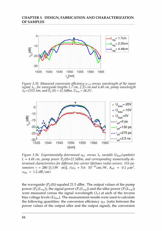
CHAPTER 3. DESIGN, FABRICATION AND CHARACTERIZATIONOF SAMPLES
λs[nm]
1535 1540 1545 1550 1555 1560 1565
ηL
L[d
B]
-30
-20
-10
0L
wg= 1.7cm
Lwg
= 2.25cm
Lwg
= 4.48cm
Figure 3.35: Measured conversion efficiency η LL versus wavelength of the input signal λs , for waveguide lengths 1.7 cm, 2.25 cm and 4.48 cm, pump wavelength λp =1552 nm, and Pp (0) = 21.5dBm, Ubias = 28.2V .
λ[nm]
1535 1540 1545 1550 1555 1560 1565
ηLL[d
B]
-30
-25
-20
-15
-10
-5U
bias=-20V
Ubias
=-10V
Ubias
=0V
τeff
=0 ps
τeff
=130 ps
τeff
=270 ps
τeff
=3.5 ns
Figure 3.36: Experimentally determined ηLL versus λs variable Ubias (symbols)L = 4.48 cm, pump power Pp (0)=21.5dBm, and corresponding numerically de-termined characteristics for different free carrier lifetimes (solid curves). (Fit pa-rameters γ = 280 [1/(W · m)], βTPA = 5.6 · 10−10cm/W , Aeff = 0.1 µm2,αlin = 1.2 dB/cm)
the waveguide (Pp (0)) equaled 21.5 dBm . The output values of the pumppower (Pp (Lwg )), the signal power (Ps (Lwg )) and the idler power (Pi (Lwg ))were measured versus the signal wavelength (λs ) at each of the reversebias voltage levels (Ubias ). The measurement results were used to calculatethe following quantities: the conversion efficiency ηLL (ratio between thepower values of the output idler and the output signal), the conversion
84
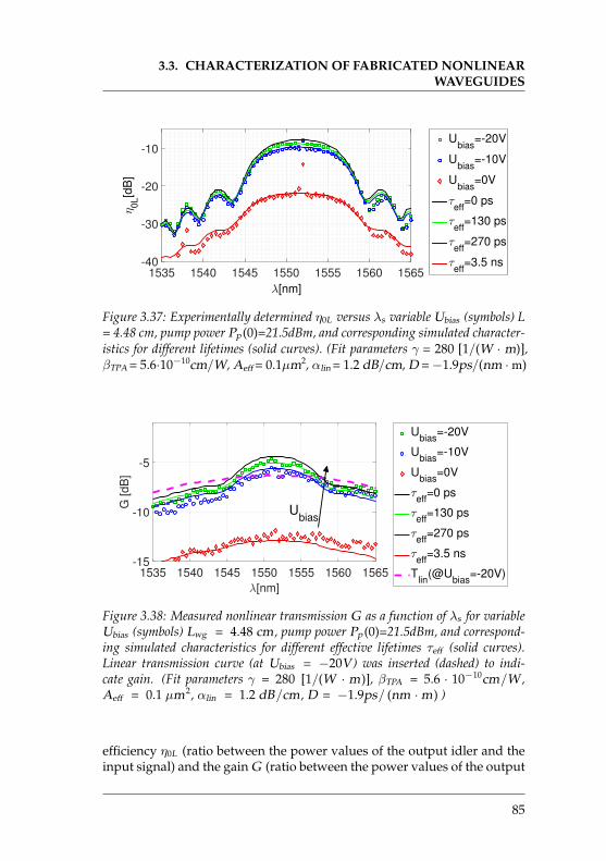
3.3. CHARACTERIZATION OF FABRICATED NONLINEARWAVEGUIDES
λ[nm]
1535 1540 1545 1550 1555 1560 1565
η0L[d
B]
-40
-30
-20
-10U
bias=-20V
Ubias
=-10V
Ubias
=0V
τeff
=0 ps
τeff
=130 ps
τeff
=270 ps
τeff
=3.5 ns
Figure 3.37: Experimentally determined η0L versus λs variable Ubias (symbols) L = 4.48 cm, pump power Pp (0)=21.5dBm, and corresponding simulated character-istics for different lifetimes (solid curves). (Fit parameters γ = 280 [1/(W · m)], βTPA = 5.6·10−10cm/W, Aeff = 0.1µm2, αlin = 1.2 dB/cm, D = −1.9ps/(nm · m)
1535 1540 1545 1550 1555 1560 1565
[nm]
-15
-10
-5
G [
dB
]
Ubias
=-20V
Ubias
=-10V
Ubias
=0V
eff=0 ps
eff=130 ps
eff=270 ps
eff=3.5 ns
Tlin
(@Ubias
=-20V)
Ubias
Figure 3.38: Measured nonlinear transmission G as a function of λs for variableUbias (symbols) Lwg = 4.48 cm , pump power Pp (0)=21.5dBm, and correspond-ing simulated characteristics for different effective lifetimes τeff (solid curves).Linear transmission curve (at Ubias = −20V ) was inserted (dashed) to indi-cate gain. (Fit parameters γ = 280 [1/(W · m)], βTPA = 5.6 · 10−10cm/W ,Aeff = 0.1 µm2, αlin = 1.2 dB/cm , D = −1.9ps/ (nm · m) )
efficiency η0L (ratio between the power values of the output idler and theinput signal) and the gain G (ratio between the power values of the output
85
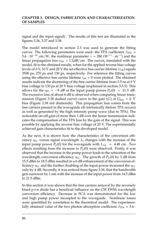
CHAPTER 3. DESIGN, FABRICATION AND CHARACTERIZATIONOF SAMPLES
signal and the input signal) . The results of this test are illustrated in thefigures 3.36, 3.37 and 3.38.
The model introduced in section 2.3 was used to generate the fittingcurves. The following parameters were used: the TPA coefficient βTPA =5.6 · 10−10 cm/W , the nonlinear parameter γ = 280 (W−1 · m−1) and thelinear propagation loss αlin = 1.2dB/cm . The curves, simulated with themodel, fit to the obtained results, when for the applied reverse bias voltagelevels of 0 V, 10 V and 20 V the set effective free carrier lifetime (τeff ) equals3500 ps, 270 ps and 130 ps, respectively. For reference the fitting curvesusing the effective free carrier lifetime τeff = 0 were plotted. The obtainedresults indicate the shortening of the free carrier lifetime from 3.5 ns at 0 Vbias voltage to 130 ps at 20 V bias voltage (explained in section 3.3.5). Thisallows for the η0L = −9 dB at the input pump power Pp (0) = 21.5 dB .The excessive loss of about 6 dB is observed when comparing linear trans-mission (Figure 3.38 dashed curve) curve to the gain (G ) at Ubias = 0 Vbias (Figure 3.38 red diamonds). This propagation loss comes from thefree carriers present in the waveguide rib intrinsically (before TPA occurs)as well as generated by the high intensity pump wave (due to TPA). Thenoticeable on-off gain of more then 1 dB over the linear transmission indi-cates the compensation of the TPA loss by the gain of the signal. This waspossible by applying the reverse bias voltage of 20 V. The experimentallyachieved gain characteristics fit to the developed model.
As the next, it is shown how the characteristics of the conversion effi-ciency ηLL versus signal wavelength λs changes with the increase of theinput pump power Pp (0) for the waveguide with Lwg = 4.48 cm . Twoeffects resulting from the increase in Pp (0) were observed. Firstly, it wasobserved that the increase in the pump power leads to the saturation of thewavelength conversion efficiency ηLL . The growth of Pp (0) by 3 dB from15.5 dBm to 18.5 dBm resulted in a 6 dB enhancement of the conversion ef-ficiency ηLL and the further doubling of the input power increased the ηLL
only by 4 dB. Secondly, it was noticed from figure 3.36, that the bandwidthgets narrower by 1 nm with the increase of the input power from 14.5 dBmto 21.5 dBm.
In this section it was shown that the free carriers removal by the reverselybised p-i-n diode has a beneficial influence on the CW FWM wavelengthconversion efficiency. Decrease in FCA was demonstrated for the lowand high pump power incoupled to the waveguide. Nonlinear losseswere quantified by correlation to the theoretical model. The experimen-tally obtained value of the two photon absorption coefficient βTPA = 5.6 ·
86
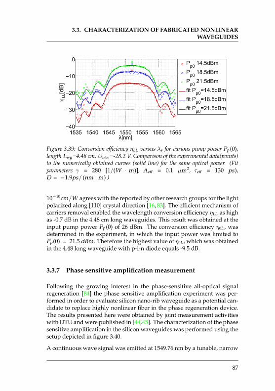
3.3. CHARACTERIZATION OF FABRICATED NONLINEARWAVEGUIDES
1535 1540 1545 1550 1555 1560 156540
30
20
10
0
λ[nm]
η[d
B]
Pp0
14.5dBm
Pp0
18.5dBm
Pp0
21.5dBm
fit Pp0
=14.5dBm
fit Pp0
=18.5dBm
fit Pp0
=21.5dBm
�LL[d
B]
Figure 3.39: Conversion efficiency ηLL versus λs for various pump power Pp (0),length Lwg =4.48 cm, Ubias =-28.2 V. Comparison of the experimental data(points)to the numerically obtained curves (solid line) for the same optical power. (Fitparameters γ = 280 [1/(W · m)], Aeff = 0.1 µm2, τeff = 130 ps),D = −1.9ps/ (nm · m) )
10−10cm/W agrees with the reported by other research groups for the lightpolarized along [110] crystal direction [16, 83]. The efficient mechanism ofcarriers removal enabled the wavelength conversion efficiency ηLL as highas -0.7 dB in the 4.48 cm long waveguides. This result was obtained at theinput pump power Pp (0) of 26 dBm. The conversion efficiency η0L , wasdetermined in the experiment, in which the input power was limited toPp (0) = 21.5 dBm . Therefore the highest value of η0L , which was obtainedin the 4.48 long waveguide with p-i-n diode equals -9.5 dB.
3.3.7 Phase sensitive amplification measurement
Following the growing interest in the phase-sensitive all-optical signalregeneration [84] the phase sensitive amplification experiment was per-formed in order to evaluate silicon nano-rib waveguide as a potential can-didate to replace highly nonlinear fiber in the phase regeneration device.The results presented here were obtained by joint measurement activitieswith DTU and were published in [44,45]. The characterization of the phasesensitive amplification in the silicon waveguides was performed using thesetup depicted in figure 3.40.
A continuous wave signal was emitted at 1549.76 nm by a tunable, narrow
87
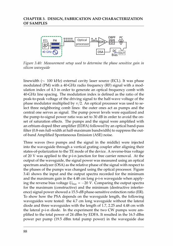
CHAPTER 3. DESIGN, FABRICATION AND CHARACTERIZATIONOF SAMPLES
DC
Bias
40 GHz
ECL PM Optical
processor
DUTOSA
EDFA
OBPF PC
Figure 3.40: Measurement setup used to determine the phase sensitive gain insilicon waveguide
linewidth (∼ 100 kHz) external cavity laser source (ECL). It was phasemodulated (PM) with a 40-GHz radio frequency (RF) signal with a mod-ulation index of 4.3 in order to generate an optical frequency comb with40-GHz line spacing. The modulation index is defined as the ratio of thepeak-to-peak voltage of the driving signal to the half-wave voltage of thephase modulator multiplied by π/2. An optical processor was used to se-lect three neighboring comb lines: the outer ones act as pumps and thecentral one serves as signal. The pump power levels were equalized andthe pump-to-signal power ratio was set to 30 dB in order to avoid the on-set of saturation effects. The pumps and the signal were amplified withan erbium-doped fiber amplifier (EDFA) followed by an optical band-passfilter (0.8-nm full-width at half-maximum bandwidth) to suppress the out-of-band Amplified Spontaneous Emission (ASE) noise.
Three waves (two pumps and the signal in the middle) were injectedinto the waveguide through a vertical grating coupler after aligning theirstates-of-polarization to the TE mode of the device. A reverse-bias voltageof 20 V was applied to the p-i-n junction for free carrier removal. At theoutput of the waveguide, the signal power was measured using an opticalspectrum analyzer (OSA) as the relative phase of the signal with respect tothe phases of the pumps was changed using the optical processor. Figure3.41 shows the input and the output spectra recorded for the minimumand the maximum gain in the 4.48 cm long p-i-n waveguide when apply-ing the reverse bias voltage Ubias = −20 V . Comparing the output spectrafor the maximum (constructive) and the minimum (destructive interfer-ence) signal power showed a 15.5-dB phase-sensitive extinction ratio (ER).To show how the PSA depends on the waveguide length, the followingwaveguides were tested: the 4.7 cm long waveguide without the lateraldiode and three waveguides with the length of 1.7, 2.25 and 4.48 cm withthe lateral p-i-n diode. In the experiment the two CW pumps were am-plified to the total power of 24 dBm by EDFA. It resulted in the 16.5 dBmpower per pump (19.5 dBm total pump power) in the waveguide due
88
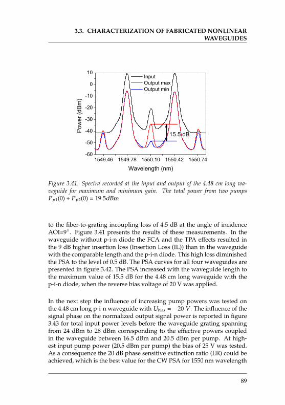
3.3. CHARACTERIZATION OF FABRICATED NONLINEARWAVEGUIDES
1549.46 1549.78 1550.10 1550.42 1550.74-60
-50
-40
-30
-20
-10
0
10
15.5 dB
Pow
er (d
Bm
)
Wavelength (nm)
Input Output max Output min
Figure 3.41: Spectra recorded at the input and output of the 4.48 cm long wa-veguide for maximum and minimum gain. The total power from two pumpsP p1(0) + P p2(0) = 19.5dBm
to the fiber-to-grating incoupling loss of 4.5 dB at the angle of incidenceAOI=9◦. Figure 3.41 presents the results of these measurements. In thewaveguide without p-i-n diode the FCA and the TPA effects resulted inthe 9 dB higher insertion loss (Insertion Loss (IL)) than in the waveguidewith the comparable length and the p-i-n diode. This high loss diminishedthe PSA to the level of 0.5 dB. The PSA curves for all four waveguides arepresented in figure 3.42. The PSA increased with the waveguide length tothe maximum value of 15.5 dB for the 4.48 cm long waveguide with thep-i-n diode, when the reverse bias voltage of 20 V was applied.
In the next step the influence of increasing pump powers was tested onthe 4.48 cm long p-i-n waveguide with Ubias = −20 V . The influence of thesignal phase on the normalized output signal power is reported in figure3.43 for total input power levels before the waveguide grating spanningfrom 24 dBm to 28 dBm corresponding to the effective powers coupledin the waveguide between 16.5 dBm and 20.5 dBm per pump. At high-est input pump power (20.5 dBm per pump) the bias of 25 V was tested.As a consequence the 20 dB phase sensitive extinction ratio (ER) could beachieved, which is the best value for the CW PSA for 1550 nm wavelength
89
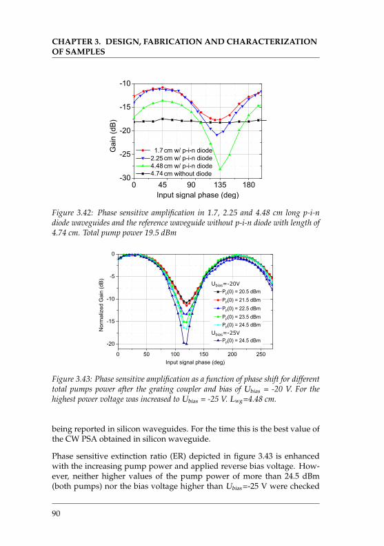
CHAPTER 3. DESIGN, FABRICATION AND CHARACTERIZATIONOF SAMPLES
1.7
2.25
4.74
4.48
Figure 3.42: Phase sensitive amplification in 1.7, 2.25 and 4.48 cm long p-i-ndiode waveguides and the reference waveguide without p-i-n diode with length of4.74 cm. Total pump power 19.5 dBm
Pp(0) = 20.5 dBm
Pp(0) = 21.5 dBm
Pp(0) = 22.5 dBm
Pp(0) = 23.5 dBm
Pp(0) = 24.5 dBm
Pp(0) = 24.5 dBm
Ubias=-20V
Ubias=-25V
Figure 3.43: Phase sensitive amplification as a function of phase shift for differenttotal pumps power after the grating coupler and bias of Ubias = -20 V. For thehighest power voltage was increased to Ubias = -25 V. Lwg =4.48 cm.
being reported in silicon waveguides. For the time this is the best value ofthe CW PSA obtained in silicon waveguide.
Phase sensitive extinction ratio (ER) depicted in figure 3.43 is enhancedwith the increasing pump power and applied reverse bias voltage. How-ever, neither higher values of the pump power of more than 24.5 dBm(both pumps) nor the bias voltage higher than Ubias =-25 V were checked
90
3.3. CHARACTERIZATION OF FABRICATED NONLINEARWAVEGUIDES
during the measurement. The lack of the saturation trend in the ER, sug-gests that the pump power and the reverse bias voltage can be increased,in order to achieve an even higher PSA extinction ratio.
3.3.8 Summary of CW FWM and PSA measurement
In this chapter the highest CW ηLL around λ = 1550 nm wavelength wasdemonstrated, to our best knowledge. The description of the CW FWMwavelength conversion as a function of the pump power, applied voltageand waveguide length is provided. In section 3.3.7 the first demonstra-tion of the phase sensitive amplification extinction ratio (ER) as high as20 dB in the silicon p-i-n nano-rib waveguide is demonstrated aroundλ = 1550 nm wavelength.
91

4System oriented experiments of wavelength
conversion
According to the results obtained in chapter 3 the silicon waveguidesproved to be efficient wavelength converters even in the telecommuni-cation range where they suffer from the two photon absorption (TPA)and the TPA induced free carrier absorption (FCA). These two mecha-nisms limit the CW wavelength conversion in the silicon waveguidesunless a lateral p-i-n diode is used. The reverse biasing of the diode, byremoving the free carriers from the waveguide, limited significantly thedetrimental influence of the TPA induced FCA. As shown in section 2.2.3an appropriate design of the waveguide and the choice of the coveringlayers results in a broader bandwidth of the conversion efficiency. Thelow linear loss αlin of the waveguide needs to be assured by suitable fab-rication in order to obtain the high efficiency of the pumping. The highlyefficient fiber-to-waveguide coupling must be granted as well, in order toavoid the high insertion loss of the nonlinear waveguide to the system.With the setup applied in this research project, however, the incouplingloss over the 10 nm conversion efficiency bandwidth reached a level overαGRC = −4.5 dB/coupler . In this research it was demonstrated for thefirst time that, even with such a level of the incoupling loss, the amplitudemodulated signal experienced a highly efficient wavelength conversionand the phase modulated signal was regenerated.
This chapter describes two possibilities to use the silicon waveguide in thetelecommunication system at the wavelengths around 1550 nm. In the firstexperiment, the amplitude modulated signal was converted using the fourwave mixing (FWM) wavelength conversion mechanism. The experimentwas performed on the signal modulated with 40 Gbps non-return to zero
93
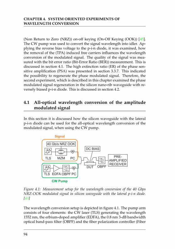
CHAPTER 4. SYSTEM ORIENTED EXPERIMENTS OFWAVELENGTH CONVERSION
(Non Return to Zero (NRZ)) on-off keying (On-Off Keying (OOK)) [43].The CW pump was used to convert the signal wavelength into idler. Ap-plying the reverse bias voltage to the p-i-n diode, it was examined, howthe removal of the (TPA) induced free carriers influences the wavelengthconversion of the modulated signal. The quality of the signal was mea-sured with the bit error ratio (Bit-Error Ratio (BER)) measurement. This isdiscussed in section 4.1. The high extinction ratio (ER) of the phase sen-sitive amplification (PSA) was presented in section 3.3.7. This indicatedthe possibility to regenerate the phase modulated signal. Therefore, thesecond experiment, which is described in this chapter examined the phasemodulated signal regeneration in the silicon nano-rib waveguide with re-versely biased p-i-n diode. This is discussed in section 4.2.
4.1 All-optical wavelength conversion of the amplitudemodulated signal
In this section it is discussed how the silicon waveguide with the lateralp-i-n diode can be used for the all-optical wavelength conversion of themodulated signal, when using the CW pump.
DC BIAS
TLS EDFA OBPF PC
DUT OBPF
PRE-
AMPLIFIED
RECEIVER
CW Pump
TLS PCMZM
40 Gb/s NRZ OOK
Signal
Figure 4.1: Measurement setup for the wavelength conversion of the 40 GbpsNRZ-OOK modulated signal in silicon waveguide with the lateral p-i-n diode.[43]
The wavelength conversion setup is depicted in figure 4.1. The pump armconsists of four elements: the CW laser (TLS) generating the wavelength1552 nm, the erbium-doped amplifier (EDFA), the 0.8 nm 3-dB bandwidthoptical band-pass filter (OBPF) and the fiber polarization controller (Fiber
94
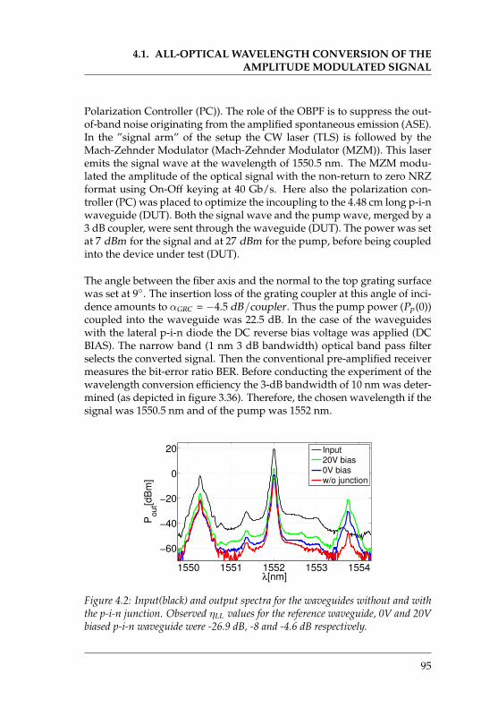
4.1. ALL-OPTICAL WAVELENGTH CONVERSION OF THEAMPLITUDE MODULATED SIGNAL
Polarization Controller (PC)). The role of the OBPF is to suppress the out-of-band noise originating from the amplified spontaneous emission (ASE).In the ”signal arm” of the setup the CW laser (TLS) is followed by theMach-Zehnder Modulator (Mach-Zehnder Modulator (MZM)). This laseremits the signal wave at the wavelength of 1550.5 nm. The MZM modu-lated the amplitude of the optical signal with the non-return to zero NRZformat using On-Off keying at 40 Gb/s. Here also the polarization con-troller (PC) was placed to optimize the incoupling to the 4.48 cm long p-i-nwaveguide (DUT). Both the signal wave and the pump wave, merged by a3 dB coupler, were sent through the waveguide (DUT). The power was setat 7 dBm for the signal and at 27 dBm for the pump, before being coupledinto the device under test (DUT).
The angle between the fiber axis and the normal to the top grating surfacewas set at 9◦. The insertion loss of the grating coupler at this angle of inci-dence amounts to αGRC = −4.5 dB/coupler . Thus the pump power (Pp (0))coupled into the waveguide was 22.5 dB. In the case of the waveguideswith the lateral p-i-n diode the DC reverse bias voltage was applied (DCBIAS). The narrow band (1 nm 3 dB bandwidth) optical band pass filterselects the converted signal. Then the conventional pre-amplified receivermeasures the bit-error ratio BER. Before conducting the experiment of thewavelength conversion efficiency the 3-dB bandwidth of 10 nm was deter-mined (as depicted in figure 3.36). Therefore, the chosen wavelength if thesignal was 1550.5 nm and of the pump was 1552 nm.
1550 1551 1552 1553 1554
−60
−40
−20
0
20
λ[nm]
Pout[d
Bm
]
Input20V bias
0V biasw/o junction
Figure 4.2: Input(black) and output spectra for the waveguides without and withthe p-i-n junction. Observed ηLL values for the reference waveguide, 0V and 20Vbiased p-i-n waveguide were -26.9 dB, -8 and -4.6 dB respectively.
95
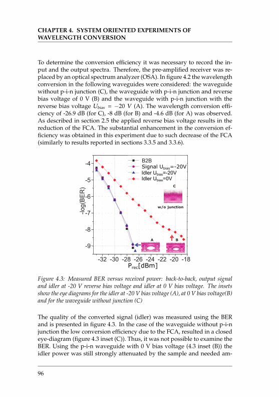
CHAPTER 4. SYSTEM ORIENTED EXPERIMENTS OFWAVELENGTH CONVERSION
To determine the conversion efficiency it was necessary to record the in-put and the output spectra. Therefore, the pre-amplified receiver was re-placed by an optical spectrum analyzer (OSA). In figure 4.2 the wavelengthconversion in the following waveguides were considered: the waveguidewithout p-i-n junction (C), the waveguide with p-i-n junction and reversebias voltage of 0 V (B) and the waveguide with p-i-n junction with thereverse bias voltage Ubias = −20 V (A). The wavelength conversion effi-ciency of -26.9 dB (for C), -8 dB (for B) and -4.6 dB (for A) was observed.As described in section 2.5 the applied reverse bias voltage results in thereduction of the FCA. The substantial enhancement in the conversion ef-ficiency was obtained in this experiment due to such decrease of the FCA(similarly to results reported in sections 3.3.5 and 3.3.6).
-32 -30 -28 -26 -24 -22 -20 -18
- 9
-8
-7
-6
-5
-4
-log
(BE
R)
Prec[dBm]
B2B
Idler Ubias=0V
A
C
B
w/o junction
Idler Ubias=-20V
Signal Ubias=-20V
Figure 4.3: Measured BER versus received power: back-to-back, output signaland idler at -20 V reverse bias voltage and idler at 0 V bias voltage. The insetsshow the eye diagrams for the idler at -20 V bias voltage (A), at 0 V bias voltage(B)and for the waveguide without junction (C)
The quality of the converted signal (idler) was measured using the BERand is presented in figure 4.3. In the case of the waveguide without p-i-njunction the low conversion efficiency due to the FCA, resulted in a closedeye-diagram (figure 4.3 inset (C)). Thus, it was not possible to examine theBER. Using the p-i-n waveguide with 0 V bias voltage (4.3 inset (B)) theidler power was still strongly attenuated by the sample and needed am-
96
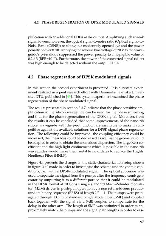
4.2. PHASE REGENERATION OF DPSK MODULATED SIGNALS
plification with an additional EDFA at the output. Amplifying such a weaksignal lowers, however, the optical signal-to-noise ratio (Optical Signal-to-Noise Ratio (OSNR)) resulting in a moderately opened eye and the powerpenalty of over 8 dB. Applying the reverse bias voltage of 20 V to the wave-guide’s p-i-n diode suppressed the power penalty to a negligible value of0.2 dB (BER=10−9). Furthermore, the power of the converted signal (idler)was high enough to be detected without the output EDFA.
4.2 Phase regeneration of DPSK modulated signals
In this section the second experiment is presented. It is a system exper-iment realized in a joint research effort with Danmarks Tekniske Univer-sitet DTU, published in [45]. This system experiment examined the phaseregeneration of the phase modulated signal.
The results presented in section 3.3.7 indicate that the phase sensitive am-plification in the silicon waveguide can be used for the phase squeezingand thus for the phase regeneration of the DPSK signal. Moreover, fromthe results it can be concluded that some improvements of the nano-ribsilicon waveguide with the p-i-n junction are inevitable to make it com-petitive against the available solutions for a DPSK signal phase regenera-tion. The following could be improved: the coupling efficiency could beincreased, the linear loss could be decreased as well as the geometry couldbe adapted in order to obtain the anomalous dispersion. The large Kerr co-efficient and the high light confinement which is possible in the nano-ribwaveguides would make them suitable candidates to replace the HighlyNonlinear Fiber (HNLF).
Figure 4.4 presents the changes in the static characterization setup shownin figure 3.40 made in order to investigate the scheme under dynamic con-ditions, i.e. with a DPSK-modulated signal. The optical processor wasused to separate the signal from the pumps after the frequency comb gen-erator by outputting it to a different port so that it could be modulatedin the DPSK format at 10 Gbps using a standard Mach-Zehnder modula-tor (MZM) driven in push-pull operation by a non return-to-zero pseudo-random binary sequence (PRBS) of length 215 − 1. The pumps were prop-agated through 13.5 m of standard Single Mode Fiber (SMF) and coupledback together with the signal via a 3-dB coupler, to compensate for thedelay in the other arm. The length of SMF was optimized in order to ap-proximately match the pumps and the signal path lengths in order to ease
97
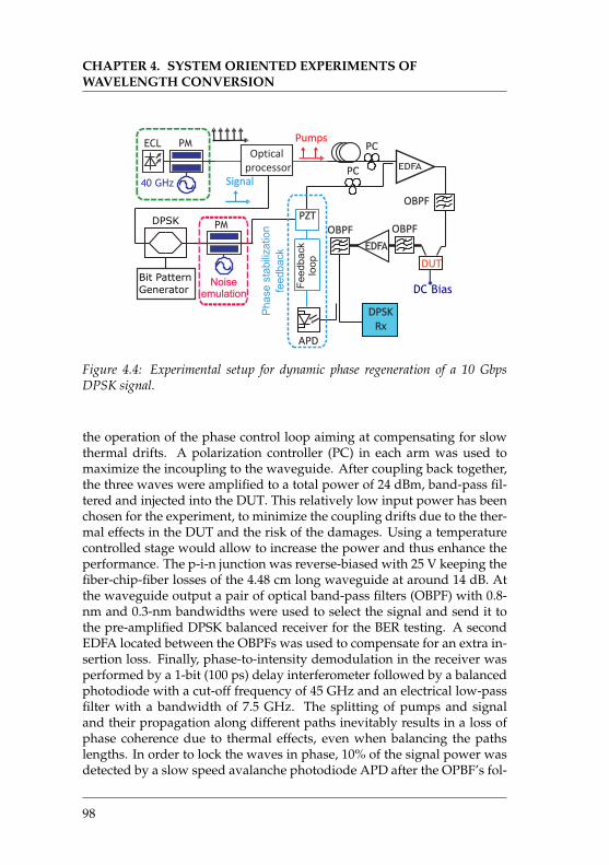
CHAPTER 4. SYSTEM ORIENTED EXPERIMENTS OFWAVELENGTH CONVERSION
DPSK
Rx
40 GHz
ECL PM
Optical
processor
DUT
DC Bias
Pumps
Signal
PM
PC
PC EDFA
OBPF
OBPF
EDFA
OBPF
APD
PZT
Fe
ed
ba
ck
loo
p
Noiseemulation
Phase s
tabili
zation
feedback
Bit Pattern
Generator
DPSK
Figure 4.4: Experimental setup for dynamic phase regeneration of a 10 GbpsDPSK signal.
the operation of the phase control loop aiming at compensating for slowthermal drifts. A polarization controller (PC) in each arm was used tomaximize the incoupling to the waveguide. After coupling back together,the three waves were amplified to a total power of 24 dBm, band-pass fil-tered and injected into the DUT. This relatively low input power has beenchosen for the experiment, to minimize the coupling drifts due to the ther-mal effects in the DUT and the risk of the damages. Using a temperaturecontrolled stage would allow to increase the power and thus enhance theperformance. The p-i-n junction was reverse-biased with 25 V keeping thefiber-chip-fiber losses of the 4.48 cm long waveguide at around 14 dB. Atthe waveguide output a pair of optical band-pass filters (OBPF) with 0.8-nm and 0.3-nm bandwidths were used to select the signal and send it tothe pre-amplified DPSK balanced receiver for the BER testing. A secondEDFA located between the OBPFs was used to compensate for an extra in-sertion loss. Finally, phase-to-intensity demodulation in the receiver wasperformed by a 1-bit (100 ps) delay interferometer followed by a balancedphotodiode with a cut-off frequency of 45 GHz and an electrical low-passfilter with a bandwidth of 7.5 GHz. The splitting of pumps and signaland their propagation along different paths inevitably results in a loss ofphase coherence due to thermal effects, even when balancing the pathslengths. In order to lock the waves in phase, 10% of the signal power wasdetected by a slow speed avalanche photodiode APD after the OPBF’s fol-
98
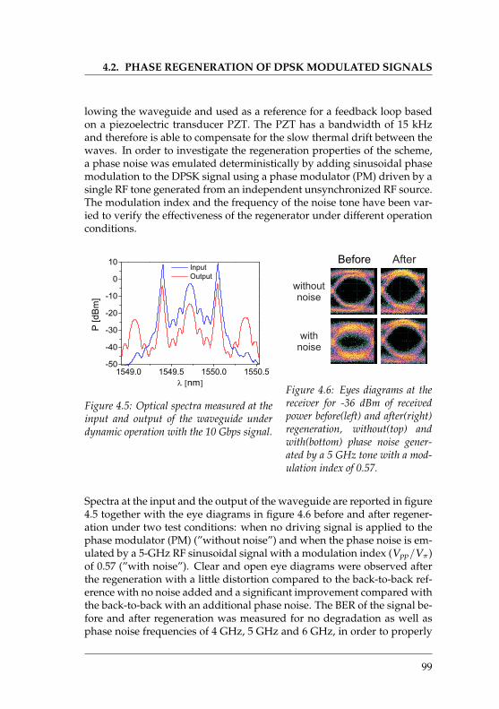
4.2. PHASE REGENERATION OF DPSK MODULATED SIGNALS
lowing the waveguide and used as a reference for a feedback loop basedon a piezoelectric transducer PZT. The PZT has a bandwidth of 15 kHzand therefore is able to compensate for the slow thermal drift between thewaves. In order to investigate the regeneration properties of the scheme,a phase noise was emulated deterministically by adding sinusoidal phasemodulation to the DPSK signal using a phase modulator (PM) driven by asingle RF tone generated from an independent unsynchronized RF source.The modulation index and the frequency of the noise tone have been var-ied to verify the effectiveness of the regenerator under different operationconditions.
1549.0 1549.5 1550.0 1550.5-50
-40
-30
-20
-10
0
10
P [d
Bm
]
[nm]
Input Output
Figure 4.5: Optical spectra measured at theinput and output of the waveguide underdynamic operation with the 10 Gbps signal.
Before After
without
noise
with
noise
Figure 4.6: Eyes diagrams at thereceiver for -36 dBm of receivedpower before(left) and after(right)regeneration, without(top) andwith(bottom) phase noise gener-ated by a 5 GHz tone with a mod-ulation index of 0.57.
Spectra at the input and the output of the waveguide are reported in figure4.5 together with the eye diagrams in figure 4.6 before and after regener-ation under two test conditions: when no driving signal is applied to thephase modulator (PM) (”without noise”) and when the phase noise is em-ulated by a 5-GHz RF sinusoidal signal with a modulation index (Vpp/Vπ)of 0.57 (”with noise”). Clear and open eye diagrams were observed afterthe regeneration with a little distortion compared to the back-to-back ref-erence with no noise added and a significant improvement compared withthe back-to-back with an additional phase noise. The BER of the signal be-fore and after regeneration was measured for no degradation as well asphase noise frequencies of 4 GHz, 5 GHz and 6 GHz, in order to properly
99
CHAPTER 4. SYSTEM ORIENTED EXPERIMENTS OFWAVELENGTH CONVERSION
assess the regenerating performance of the waveguide. All the measure-ments have been carried out keeping the modulation index (Vpp/Vπ) ofthe phase noise fixed at 0.57.
-45 -42 -39 -36 -33 -30 -271110987654
3
2
Before After reg. No noise 4 GHz noise 5 GHz noise 6 GHz noise
-log(
BE
R)
Prec [dBm]
Figure 4.7: BER as a function of the re-ceived power for different phase noiseloading conditions before (solid sym-bols) and after (hollow symbols) regen-eration. Modulation index of 0.57 wasused.
0.0 0.2 0.4 0.6 0.802468
101214161860
Pow
er p
enal
ty (d
B)
Noise modulation index (Vpp/V )
Before regeneration After regeneration
+Inf
Figure 4.8: Power penalty (comparedto back-to-back for a BER=10−9) as afunction of the modulation index of the5-GHz radio frequency tone used toemulate the phase noise
The resulting BER curves as a function of the received power are shownin figure 4.7. In the absence of added noise, the scheme results in a powerpenalty of around 1 dB with respect to the back-to-back reference takenat the powermeter (PM) output. However, when phase noise is added tothe signal, the regenerated output shows an improved receiver sensitivity(defined at a BER = 10−9) for all the three considered ”phase noise” fre-quencies, enabling to decrease the power penalty from 10 dB down to lessthan 3.5 dB. The degradation caused by increasing the noise frequency ispartially mitigated by the electrical low-pass filter at the receiver. This canbe observed on the BER plots of the signal before regeneration. No signif-icant correlation can be seen between the performances of the regeneratedoutput and the frequency chosen for the noise emulation. The last aspectthat was investigated was the impact of the modulation index on the re-generation performance for a fixed noise frequency (5 GHz). The powerpenalty at BER = 10−9 with respect to back-to-back without degradationis reported in figure 4.8 as a function of the modulation index, before andafter regeneration. The results show that an increase of the phase noisemodulation index causes a slow increase in the power penalty for the re-
100

4.2. PHASE REGENERATION OF DPSK MODULATED SIGNALS
generated signal. The degradation, however, advances faster for the signalwithout regeneration. This leads to an error floor at a BER = 10−3 whenthe modulation index of the RF tone reaches 0.78. The corresponding re-generated signal can achieve error-free performances with a penalty below6 dB.
101

5State of the Art
In this thesis we investigated possibilities enabled by integration of thep-i-n junction with the silicon nano-rib waveguide. For the wavelengthsaround 1.55 µm silicon exhibits TPA and thus also FCA effects due to itsenergy bandgap [27, 35, 85–87]. This impeded its applicability for the non-linear application.
With limited FCA the nonlinearity of silicon allows for efficient wave-length conversion as well as PSA and PSA based signal regeneration. Eventhough its nonlinearity coefficient γ is lower than the maximum achievedin α-Si, crystalline silicon offers stability of material properties and re-liability. Well known technology used for electronics circuitry enablesmonolithic integration of optical and electronic circuits on one SOI chip.The platform also offers the possibility to engineer dispersion and lossby change in the waveguide dimensions and claddings and thus enhancenonlinear properties [48, 52, 87].
Two approaches not requiring technology effort were so far used to bypassTPA and FCA. One, was to operate in the pulse mode with the repetitionrate low enough (e.g tens of MHz) to avoid the accumulation of the elec-trons and holes in the waveguide region [88]. The second is to operate inthe mid-infrared wavelength range [89] escaping from TPA and thus fromFCA as well. Many research groups moved towards wavelengths longerthan 2 µm [90, 91]. Both of these methods, however, exclude applicationsdemanding continuous wave (CW) operation in telecommunication wa-velength range around 1550 nm. The remaining method to suppress FCAis to decrease free carrier lifetime. Several groups have doped silicon wa-veguides with variety of ions to create recombination centers for electronsand holes. Early promissing results were obtained with the He ions by
103
CHAPTER 5. STATE OF THE ART
Liu and Tsang [66] where the reported effective lifetime of carriers was de-creased from 100 to 1.9 ns with increase of propagation loss of about 0.3dB/cm due to implant dosis of 1012cm−2. The solutions with other ionse.g. Au [67], Ar [68], O [69, 70] or Si [71] decreasing FCA increased thepropagation loss due to scattering from implants. The severe decrease intransmission through the doped waveguides makes the devices in most ofthe cases unfeasible.
The active carrier removal with the p-i-n diode along the waveguide pro-posed by Rong et al. [38, 64, 72, 73] proved to be the direction to follow indecreasing concentration of the electrons and holes in the waveguide. Ap-plying this method, the continuous wave (CW) Raman laser was demon-strated and enabled an efficient continuous-wave wavelength conversionvia FWM. However, at the beginning of this work only relatively low wa-velength conversion efficiencies had been reported in silicon waveguides.Malouthi et al. [65] reported an efficiency of -5.5 dB, and before that, Ronget al. obtained 8.5 dB in waveguides with 1.5 × 1.5µm rib waveguideswith p-i-n [72]. To the best of my knowledge there was no report of highefficiency CW FWM at 1550 nm in nano-rib p-i-n waveguides until thiswork. In parallel to the work on this thesis Ong et al. presented the re-sults of -4.4 dB [59]). The authors used only 160 mW in the waveguideand it is not sure why they did not exceed this power. Hence the highestCW conversion efficiency around 1550 nm wavelength to the best of myknowledge was reported in [61] and contributed to this thesis. Major re-sults reported in the literature on the CW FWM conversion efficiency aresummarized in the Table 5.1. The conversion efficiency ηLL is output idlerto output signal conversion efficiency (imbalance between output at thesignal wavelength originally coupled into the waveguide and the powermeasured at the idler (converted via FWM process)) , αlin is the linear losscoefficient, λPump the pump wavelength and L is the waveguide length.
104
Max.ηLL
[dB]
αlin
[dB ·cm−1]
λp
[nm](Pp0
[mW])
Wwg xHwg x swg
[nm]
Lwg
[cm]
Wave-guidetype
Ubias
[V]Year[Ref.]
-8.6 0.4 1550(450)
1500 x1500 x 700 8 SOI
rib -25 2006[42]
-4.4 0.74 1550(160) 650x220 6.35 SOI
rib -20 2013[59]
-0.7 0.9 1552(400) 500x220 4.0 SOI
rib -202012Thiswork
-9.6 <1.5 1550(110) 500 x 300 1.8 SOI
wire - 2007[48]
-5.5 0.6 1552.12(320)
600 x 340x 210 2.5 SOI
rib - 2008[65]
-40 15 1550(35) 589 x 2201 0.4 slot - 2009
[33]
Table 5.1: Comparison of the CW wavelength conversion in SOI waveguidesaround the 1.5 µm wavelength. Given value of the bias voltage indicates pres-ence of the lateral p-i-n diode.
105

6Conclusions
At the beginning of the thesis the state-of-the-art in the nonlinear opticalplatforms was discussed. It was also explained why from these platformsthe silicon on insulator (SOI) was selected. Furthermore, the disadvan-tages and advantages of the silicon material in respect to supporting non-linear optical effects were discussed. The following disadvantages wereidentified: the linear loss, the two photon absorption (TPA) and the TPAinduced free carrier absorption (FCA). On the other hand the advanta-geous properties of silicon were listed. First and the most important ad-vantage is the high nonlinear optical Kerr coefficient around the 1550 nmwavelength. The high refractive index makes it possible to confine thelight in the sub-micron cross-section of the waveguide. The high confine-ment with the high nonlinear optical Kerr coefficient leads to the high non-linear coefficient (γ) of the sub-micron silicon waveguide.
Nevertheless, such high confinement results in the high light intensity inthe silicon material and gives rise to the TPA and TPA induced FCA. TheTPA results from the energy bandgap. The light at the wavelength around1550 nm propagating through the silicon waveguide at a sufficiently highpower causes additional loss. This loss cannot be avoided at this wave-length range. The TPA induced FCA, however, can be substantially de-creased. The other important factor considering nonlinear optical effectin silicon is an optical dispersion. To support four wave mixing in thesilicon waveguide the anomalous dispersion is preferred. Although thesilicon material is characterized with the normal dispersion, the anoma-lous dispersion can be obtained by constructing of the suitable shape anddimensions of the waveguide.
In the theoretical part of this thesis the optical properties of the silicon and
107
CHAPTER 6. CONCLUSIONS
the propagation of the wave in the nonlinear Kerr medium were intro-duced. With this background it was possible to define the direction of thesilicon waveguide development in order to support the FWM effect. Thesub-micron waveguide cross-section was chosen to assure the small non-linear effective area. Moreover, the impact of the following parameters onthe waveguide dispersion was examined: the width of the rib, the heightof the rib, the thickness of the slab and the material covering the wave-guide. The calculations results showed which dimensions can be used inorder to obtain the anomalous dispersion in a silicon nano-rib waveguide.Additionally, it became clear that the free carriers substantially contributeto propagation loss while the light with a high power is sent through thewaveguide. Thus, a suitable method of the free carriers removal from thewaveguide had to be chosen. For this purpose ? the lateral p-i-n juctionwas added along the waveguide structure.
The electrical simulations performed within this thesis resulted in the de-sign of the lateral p-i-n diode, which efficiently removes the free carriersfrom the waveguide region. In this place it must be mentioned that theelectrical calculation contained some simplifications and did not fully fit tothe measured values. Nevertheless the trends obtained from simulationswere experimentally confirmed. It was also analyzed how the optical lossdepends on the overlap of the mode of the light with the doped regions ofthe lateral diode.
The simulations performed in the theoretical part of the research were ap-plied to design the nano-rib silicon waveguide with the lateral p-i-n diode.The waveguides were realized in the BiCMOS pilot line at Leibniz Insti-tute IHP in Franfurt(Oder). The height of the waveguides was enforcedby the technology used for fabrication and the realization of the experi-mental samples within the multi-purpose wafer. This height assured thewaveguides with the low linear loss.
When measuring the loss it was observed that the free carriers werepresent in the waveguides even before the use of the high power of thelight. The measured optical loss of the waveguides without the bias volt-age amounted to 2.1 dB/cm. Applying the reverse bias voltage to the p-i-ndiode lateral to the waveguide allowed to decrease the loss to the level ofbelow 1 dB/cm. The dispersion of the silicon nano-rib waveguides wasmeasured using the MZI structures fabricated together with the wave-guides. The measured value of the dispersion coefficient D = −1.6ps/n ·mfor the waveguides with the height of 220 nm at the wavelength of 1550nm. The result falls in between the values determined in the simulations
108
and taking into account only single nitride or single oxide cladding. Thefabricated sample, however, had both oxide and nitride cladding on topof the waveguide rib. The higher waveguides confirmed the simulatedvalues. The waveguide with the rib height of 300 nm exhibits very lownormal dispersion and the waveguides with the rib height of 400 nmexhibit the anomalous dispersion.
In order to achieve the FWM in the silicon waveguide the high powerlight was coupled into the waveguide. Under this condition additionalloss mechanisms became important, which are present in the silicon wa-veguide. These were the TPA and the TPA induced FCA. The two mech-anisms are dependent on the optical power coupled into the waveguide.Therefore they were characterized at the different power levels of the lightcoupled into the waveguide. Later, several experiments were conducted,in order to use the potentially high FWM effect in the silicon waveguide toconvert the wavelength of light. The strength of the FWM effect dependson the phase shift between the high power light at one wavelength andthe week power light at another wavelength. Hence, measurements of thePSA were performed.
The nonlinear properties of the silicon nano-rib waveguides were char-acterized in several experiments. The experiments were performed withthe CW pump light at the wavelength around 1550 nm. The CW FWMwavelength conversion efficiency ηLL equals -0.7 dB was achieved. It isimportant to note that, this is the highest value reported until now aroundthe 1550 nm wavelength. Moreover, the 3-dB bandwidth of the conversionefficiency of 10 nm was obtained in the 220 nm high waveguides. Fur-thermore, the measurement of the PSA in the silicon waveguides with thelateral p-i-n diode was performed. In this experiment the PSA extinctionratio as high as 20 dB was obtained. It is crucial that both of this substan-tial achievements were obtained by applying the reverse bias voltage tothe lateral p-i-n diode along the waveguide.
Additionally two experiments were performed, in order to check whetherthe silicon waveguides can be used in the fiber optic telecommunicationsystem. First experiment demonstrated the wavelength conversion of the40 Gb/s NRZ OOK signal. The BER was mesured to asssess the quality ofthe converted signal. With the applied reverse bias voltage the negligiblepower penalty of 0.2 dB was achieved. Furthermore the regeneration of theDPSK modulated signal was demonstrated with the simulated sinusoidaldistortions at different frequencies and modulation depths.
109

CHAPTER 6. CONCLUSIONS
In the opinion of the author of the thesis further improvements shall befocused on the development of the high silicon nano-rib waveguide withthe lateral p-i-n diode in order to achieve the anomalous dispersion. Atthe same time the linear loss below 1 dB/cm must be assured. Providedthat the anomalous dispersion of the waveguide can be obtained and thewaveguide loss can be lowered to 0.5 dB/cm with known optical nonlin-ear limiting TPA and FCA the CW FWM gain of about 8 dB should befeasible.
110

List of Acronyms and Chemical Symbols
Acronym orChem. Symbol Description
α-Si amorphous silicon
Alx Ga1−x As aluminum gallium arsenideAPD Avalanche Photo DiodeAs arsenicAs2S3 arsenic sulfideASE Amplified Spontaneous EmissionAu gold
B boronBER Bit-Error Ratio
CPL Fiber Optic Couplerc-Si crystalline siliconCW Continuous Wave
DFG Deutsche Forschung GemeinschaftDPSK Differential Phase Shift KeyingDTU Danske Tekniske UniversitetDUT Device Under TestDUV Deep Ultra Violet
EDFA Erbium Doped Fiber AmplifierER Extinction Ratio
FCA Free Carrier Absorptionfft Fast Fourier TransformFPC Fiber Polarization ControllerFWM Four Wave Mixing
GRC Grating Coupler
HHI Fraunhofer Heinrich Herz InstituteHNLF Highly Nonlinear Fiber
ICP Inductively Coupled Plasma
111
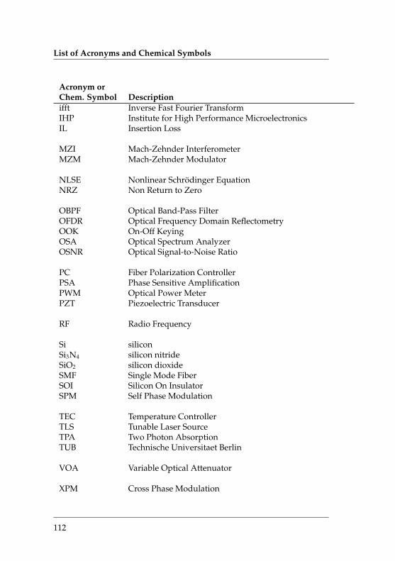
List of Acronyms and Chemical Symbols
Acronym orChem. Symbol Descriptionifft Inverse Fast Fourier TransformIHP Institute for High Performance MicroelectronicsIL Insertion Loss
MZI Mach-Zehnder InterferometerMZM Mach-Zehnder Modulator
NLSE Nonlinear Schrodinger EquationNRZ Non Return to Zero
OBPF Optical Band-Pass FilterOFDR Optical Frequency Domain ReflectometryOOK On-Off KeyingOSA Optical Spectrum AnalyzerOSNR Optical Signal-to-Noise Ratio
PC Fiber Polarization ControllerPSA Phase Sensitive AmplificationPWM Optical Power MeterPZT Piezoelectric Transducer
RF Radio Frequency
Si siliconSi3N4 silicon nitrideSiO2 silicon dioxideSMF Single Mode FiberSOI Silicon On InsulatorSPM Self Phase Modulation
TEC Temperature ControllerTLS Tunable Laser SourceTPA Two Photon AbsorptionTUB Technische Universitaet Berlin
VOA Variable Optical Attenuator
XPM Cross Phase Modulation
112
List of symbols
Symbol Description Unit
A slowly varying amplitude along z direc-tion, in this thesis relation between ampli-tude and optical power is |A |2 = P
V/cm
Aeff effective area Aeff of the waveguide (cm−2
αFCA dB absorption due to free carriers dB · cm−1
αGRC incoupling loss due to the grating coupler dB/couplerαlin linear loss dB · cm−1
αTPA loss coefficient due to TPA cm−1
β mode propagation constant m−1
β1 inverse of the group velocity s/mβ2 group velocity dispersion s2/mβn n-th order dispersion term sn/mβTPA two photon absorption coefficient m/WBW FWM bandwidth nm
χχχ optical susceptibility
d grating coupler etch depth nm∆αFCA excess propagation loss due to the presence
of free carriers∆αpin excess waveguide optical propagation loss
due to the presence of doping regions asidea waveguide
dB/cm
Dcl cladding cross-section area cm2
D differential operator used in symmetricsplit step fourier method accounting forlinear loss and dispersion
D material dispersion coefficient ps/(nm · m)D electrical displacement C/cm2
∆nFCD change in the refractive index due to thefree carriers
DSi material dispersion coefficient of silicon ps/(nm · m)DSi3N4 material dispersion coefficient of silicon ni-
trideps/(nm · m)
113
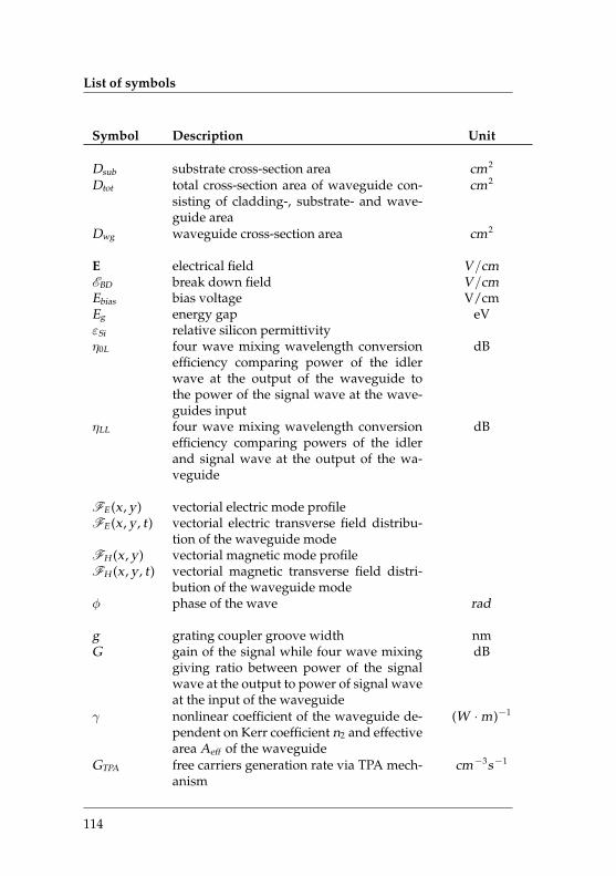
List of symbols
Symbol Description Unit
Dsub substrate cross-section area cm2
Dtot total cross-section area of waveguide con-sisting of cladding-, substrate- and wave-guide area
cm2
Dwg waveguide cross-section area cm2
E electrical field V/cmEBD break down field V/cmEbias bias voltage V/cmEg energy gap eVεSi relative silicon permittivityη0L four wave mixing wavelength conversion
efficiency comparing power of the idlerwave at the output of the waveguide tothe power of the signal wave at the wave-guides input
dB
ηLL four wave mixing wavelength conversionefficiency comparing powers of the idlerand signal wave at the output of the wa-veguide
dB
FE (x , y) vectorial electric mode profileFE (x , y , t ) vectorial electric transverse field distribu-
tion of the waveguide modeFH (x , y) vectorial magnetic mode profileFH (x , y , t ) vectorial magnetic transverse field distri-
bution of the waveguide modeϕ phase of the wave rad
g grating coupler groove width nmG gain of the signal while four wave mixing
giving ratio between power of the signalwave at the output to power of signal waveat the input of the waveguide
dB
γ nonlinear coefficient of the waveguide de-pendent on Kerr coefficient n2 and effectivearea Aeff of the waveguide
(W · m)−1
GTPA free carriers generation rate via TPA mech-anism
cm−3s−1
114
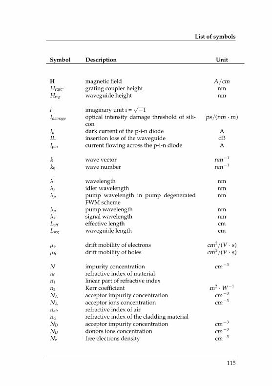
List of symbols
Symbol Description Unit
H magnetic field A/cmHGRC grating coupler height nmHwg waveguide height nm
i imaginary unit i =√−1
Idamage optical intensity damage threshold of sili-con
ps/(nm · m)
Id dark current of the p-i-n diode AIL insertion loss of the waveguide dBIpin current flowing across the p-i-n diode A
k wave vector nm−1
k0 wave number nm−1
λ wavelength nmλi idler wavelength nmλp pump wavelength in pump degenerated
FWM schemenm
λp pump wavelength nmλs signal wavelength nmLeff effective length cmLwg waveguide length cm
µe drift mobility of electrons cm2/(V · s)µh drift mobility of holes cm2/(V · s)
N impurity concentration cm−3
n0 refractive index of materialn1 linear part of refractive indexn2 Kerr coefficient m2 · W−1
NA acceptor impurity concentration cm−3
NA acceptor ions concentration cm−3
nair refractive index of airncl refractive index of the cladding materialND acceptor impurity concentration cm−3
ND donors ions concentration cm−3
Ne free electrons density cm−3
115
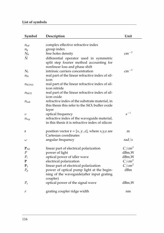
List of symbols
Symbol Description Unit
neff complex effective refractive indexng group indexNh free holes density cm−3
N differential operator used in symmetricsplit step fourier method accounting fornonlinear loss and phase shift
Ni intrinsic carriers concentration cm−3
nSi real part of the linear refractive index of sil-icon
nSi3N4 real part of the linear refractive index of sil-icon nitride
nSiO2 real part of the linear refractive index of sil-icon oxide
nsub refractive index of the substrate material, inthis thesis this refer to the SiO2 buffer oxidelayer
ν optical frequency s−1
nwg refractive index of the waveguide material,in this thesis it is refractive index of silicon
r position vector r = [x , y , z], where x,y,z areCartesian coordinates
m
ω angular frequency rad/s
PNL linear part of electrical polarization C/cm2
P power of light dBm,WPi optical power of idler wave dBm,WP electrical polarization C/cm2
PL linear part of electrical polarization C/cm2
Pp power of optical pump light at the begin-ning of the waveguide(after input gratingcoupler)
dBm
Ps optical power of the signal wave dBm,W
r grating coupler ridge width nm
116
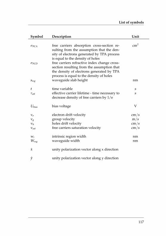
List of symbols
Symbol Description Unit
σFCA free carriers absorption cross-section re-sulting from the assumption that the den-sity of electrons generated by TPA processis equal to the density of holes
cm2
σFCD free carriers refractive index change cross-section resulting from the assumption thatthe density of electrons generated by TPAprocess is equal to the density of holes
swg waveguide slab height nm
t time variable sτeff effective carrier lifetime - time necessary to
decrease density of free carriers by 1/es
Ubias bias voltage V
ve electron drift velocity cm/svg group velocity m/svh holes drift velocity cm/svsat free carriers saturation velocity cm/s
wi intrinsic region width nmWwg waveguide width nm
x unity polarization vector along x direction
y unity polarization vector along y direction
117

List of used constants
Quantity Symbol Value
Electron-volt energy eV 1eV = 1.60218 × 10⁻¹⁹ J
Euler’s constant e ∼ 2.71828182845904...
Permeability in vacuum µ0 1.25663 × 10⁻⁸ H/cmPermittivity in vacuum ε0 8.85418 × 10⁻¹⁴ F/cmPlanck’s constant h 4.1357 × 10⁻¹⁵ eV ·s
Speed of light in vacuum c 2.99792 × 1010 cm/s
118
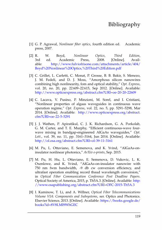
Bibliography
[1] G. P. Agrawal, Nonlinear fiber optics, fourth edition ed. Academicpress, 2007.
[2] R. W. Boyd, Nonlinear Optics, Third Edition,3rd ed. Academic Press, 2008. [Online]. Avail-able: http://www.fulviofrisone.com/attachments/article/404/Boyd%20Nonlinear%20Optics,%20Third%20Edition.pdf
[3] C. Grillet, L. Carletti, C. Monat, P. Grosse, B. B. Bakir, S. Menezo,J. M. Fedeli, and D. J. Moss, “Amorphous silicon nanowirescombining high nonlinearity, fom and optical stability,” Opt. Express,vol. 20, no. 20, pp. 22 609–22 615, Sep 2012. [Online]. Available:http://www.opticsexpress.org/abstract.cfm?URI=oe-20-20-22609
[4] C. Lacava, V. Pusino, P. Minzioni, M. Sorel, and I. Cristiani,“Nonlinear properties of algaas waveguides in continuous waveoperation regime,” Opt. Express, vol. 22, no. 5, pp. 5291–5298, Mar2014. [Online]. Available: http://www.opticsexpress.org/abstract.cfm?URI=oe-22-5-5291
[5] J. J. Wathen, P. Apiratikul, C. J. K. Richardson, G. A. Porkolab,G. M. Carter, and T. E. Murphy, “Efficient continuous-wave four-wave mixing in bandgap-engineered AlGaAs waveguides,” Opt.Lett., vol. 39, no. 11, pp. 3161–3164, Jun 2014. [Online]. Available:http://ol.osa.org/abstract.cfm?URI=ol-39-11-3161
[6] M. Pu, L. Ottaviano, E. Semenova, and K. Yvind, “AlGaAs-on-insulator nonlinear photonics,” ArXiv e-prints, Sep. 2015.
[7] M. Pu, H. Hu, L. Ottaviano, E. Semenova, D. Vukovic, L. K.Oxenlowe, and K. Yvind, “AlGaAs-on-insulator nanowire with750 nm fwm bandwidth, -9 db cw conversion efficiency, andultrafast operation enabling record tbaud wavelength conversion,”in Optical Fiber Communication Conference Post Deadline Papers.Optical Society of America, 2015, p. Th5A.3. [Online]. Available: http://www.osapublishing.org/abstract.cfm?URI=OFC-2015-Th5A.3
[8] I. Kaminow, T. Li, and A. Willner, Optical Fiber TelecommunicationsVolume VIA: Components and Subsystems, ser. Optics and Photonics.Elsevier Science, 2013. [Online]. Available: https://books.google.de/books?id=8V8LMI9WhGEC
119
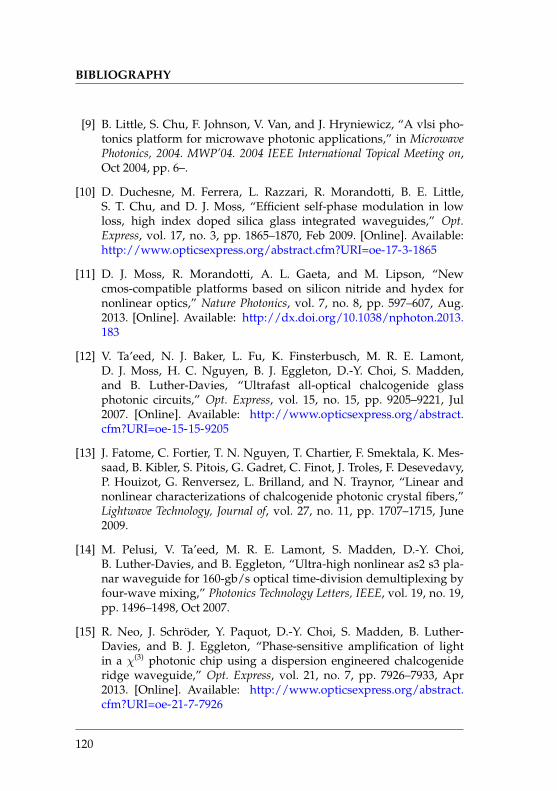
BIBLIOGRAPHY
[9] B. Little, S. Chu, F. Johnson, V. Van, and J. Hryniewicz, “A vlsi pho-tonics platform for microwave photonic applications,” in MicrowavePhotonics, 2004. MWP’04. 2004 IEEE International Topical Meeting on,Oct 2004, pp. 6–.
[10] D. Duchesne, M. Ferrera, L. Razzari, R. Morandotti, B. E. Little,S. T. Chu, and D. J. Moss, “Efficient self-phase modulation in lowloss, high index doped silica glass integrated waveguides,” Opt.Express, vol. 17, no. 3, pp. 1865–1870, Feb 2009. [Online]. Available:http://www.opticsexpress.org/abstract.cfm?URI=oe-17-3-1865
[11] D. J. Moss, R. Morandotti, A. L. Gaeta, and M. Lipson, “Newcmos-compatible platforms based on silicon nitride and hydex fornonlinear optics,” Nature Photonics, vol. 7, no. 8, pp. 597–607, Aug.2013. [Online]. Available: http://dx.doi.org/10.1038/nphoton.2013.183
[12] V. Ta’eed, N. J. Baker, L. Fu, K. Finsterbusch, M. R. E. Lamont,D. J. Moss, H. C. Nguyen, B. J. Eggleton, D.-Y. Choi, S. Madden,and B. Luther-Davies, “Ultrafast all-optical chalcogenide glassphotonic circuits,” Opt. Express, vol. 15, no. 15, pp. 9205–9221, Jul2007. [Online]. Available: http://www.opticsexpress.org/abstract.cfm?URI=oe-15-15-9205
[13] J. Fatome, C. Fortier, T. N. Nguyen, T. Chartier, F. Smektala, K. Mes-saad, B. Kibler, S. Pitois, G. Gadret, C. Finot, J. Troles, F. Desevedavy,P. Houizot, G. Renversez, L. Brilland, and N. Traynor, “Linear andnonlinear characterizations of chalcogenide photonic crystal fibers,”Lightwave Technology, Journal of, vol. 27, no. 11, pp. 1707–1715, June2009.
[14] M. Pelusi, V. Ta’eed, M. R. E. Lamont, S. Madden, D.-Y. Choi,B. Luther-Davies, and B. Eggleton, “Ultra-high nonlinear as2 s3 pla-nar waveguide for 160-gb/s optical time-division demultiplexing byfour-wave mixing,” Photonics Technology Letters, IEEE, vol. 19, no. 19,pp. 1496–1498, Oct 2007.
[15] R. Neo, J. Schroder, Y. Paquot, D.-Y. Choi, S. Madden, B. Luther-Davies, and B. J. Eggleton, “Phase-sensitive amplification of lightin a χ(3) photonic chip using a dispersion engineered chalcogenideridge waveguide,” Opt. Express, vol. 21, no. 7, pp. 7926–7933, Apr2013. [Online]. Available: http://www.opticsexpress.org/abstract.cfm?URI=oe-21-7-7926
120
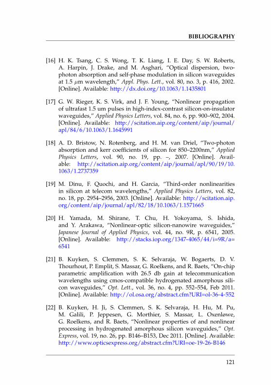
BIBLIOGRAPHY
[16] H. K. Tsang, C. S. Wong, T. K. Liang, I. E. Day, S. W. Roberts,A. Harpin, J. Drake, and M. Asghari, “Optical dispersion, two-photon absorption and self-phase modulation in silicon waveguidesat 1.5 µm wavelength,” Appl. Phys. Lett., vol. 80, no. 3, p. 416, 2002.[Online]. Available: http://dx.doi.org/10.1063/1.1435801
[17] G. W. Rieger, K. S. Virk, and J. F. Young, “Nonlinear propagationof ultrafast 1.5 um pulses in high-index-contrast silicon-on-insulatorwaveguides,” Applied Physics Letters, vol. 84, no. 6, pp. 900–902, 2004.[Online]. Available: http://scitation.aip.org/content/aip/journal/apl/84/6/10.1063/1.1645991
[18] A. D. Bristow, N. Rotenberg, and H. M. van Driel, “Two-photonabsorption and kerr coefficients of silicon for 850–2200nm,” AppliedPhysics Letters, vol. 90, no. 19, pp. –, 2007. [Online]. Avail-able: http://scitation.aip.org/content/aip/journal/apl/90/19/10.1063/1.2737359
[19] M. Dinu, F. Quochi, and H. Garcia, “Third-order nonlinearitiesin silicon at telecom wavelengths,” Applied Physics Letters, vol. 82,no. 18, pp. 2954–2956, 2003. [Online]. Available: http://scitation.aip.org/content/aip/journal/apl/82/18/10.1063/1.1571665
[20] H. Yamada, M. Shirane, T. Chu, H. Yokoyama, S. Ishida,and Y. Arakawa, “Nonlinear-optic silicon-nanowire waveguides,”Japanese Journal of Applied Physics, vol. 44, no. 9R, p. 6541, 2005.[Online]. Available: http://stacks.iop.org/1347-4065/44/i=9R/a=6541
[21] B. Kuyken, S. Clemmen, S. K. Selvaraja, W. Bogaerts, D. V.Thourhout, P. Emplit, S. Massar, G. Roelkens, and R. Baets, “On-chipparametric amplification with 26.5 db gain at telecommunicationwavelengths using cmos-compatible hydrogenated amorphous sili-con waveguides,” Opt. Lett., vol. 36, no. 4, pp. 552–554, Feb 2011.[Online]. Available: http://ol.osa.org/abstract.cfm?URI=ol-36-4-552
[22] B. Kuyken, H. Ji, S. Clemmen, S. K. Selvaraja, H. Hu, M. Pu,M. Galili, P. Jeppesen, G. Morthier, S. Massar, L. Oxenløwe,G. Roelkens, and R. Baets, “Nonlinear properties of and nonlinearprocessing in hydrogenated amorphous silicon waveguides,” Opt.Express, vol. 19, no. 26, pp. B146–B153, Dec 2011. [Online]. Available:http://www.opticsexpress.org/abstract.cfm?URI=oe-19-26-B146
121
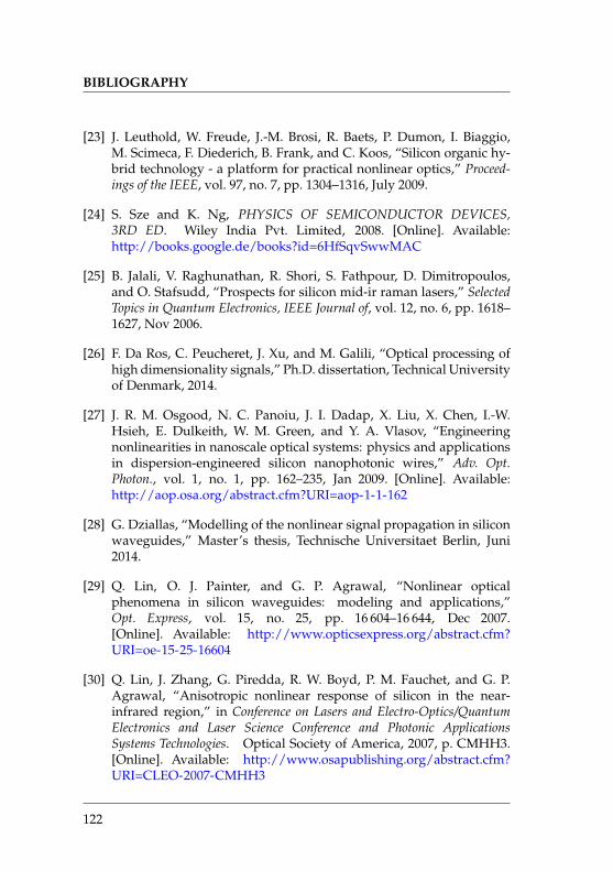
BIBLIOGRAPHY
[23] J. Leuthold, W. Freude, J.-M. Brosi, R. Baets, P. Dumon, I. Biaggio,M. Scimeca, F. Diederich, B. Frank, and C. Koos, “Silicon organic hy-brid technology - a platform for practical nonlinear optics,” Proceed-ings of the IEEE, vol. 97, no. 7, pp. 1304–1316, July 2009.
[24] S. Sze and K. Ng, PHYSICS OF SEMICONDUCTOR DEVICES,3RD ED. Wiley India Pvt. Limited, 2008. [Online]. Available:http://books.google.de/books?id=6HfSqvSwwMAC
[25] B. Jalali, V. Raghunathan, R. Shori, S. Fathpour, D. Dimitropoulos,and O. Stafsudd, “Prospects for silicon mid-ir raman lasers,” SelectedTopics in Quantum Electronics, IEEE Journal of, vol. 12, no. 6, pp. 1618–1627, Nov 2006.
[26] F. Da Ros, C. Peucheret, J. Xu, and M. Galili, “Optical processing ofhigh dimensionality signals,” Ph.D. dissertation, Technical Universityof Denmark, 2014.
[27] J. R. M. Osgood, N. C. Panoiu, J. I. Dadap, X. Liu, X. Chen, I.-W.Hsieh, E. Dulkeith, W. M. Green, and Y. A. Vlasov, “Engineeringnonlinearities in nanoscale optical systems: physics and applicationsin dispersion-engineered silicon nanophotonic wires,” Adv. Opt.Photon., vol. 1, no. 1, pp. 162–235, Jan 2009. [Online]. Available:http://aop.osa.org/abstract.cfm?URI=aop-1-1-162
[28] G. Dziallas, “Modelling of the nonlinear signal propagation in siliconwaveguides,” Master’s thesis, Technische Universitaet Berlin, Juni2014.
[29] Q. Lin, O. J. Painter, and G. P. Agrawal, “Nonlinear opticalphenomena in silicon waveguides: modeling and applications,”Opt. Express, vol. 15, no. 25, pp. 16 604–16 644, Dec 2007.[Online]. Available: http://www.opticsexpress.org/abstract.cfm?URI=oe-15-25-16604
[30] Q. Lin, J. Zhang, G. Piredda, R. W. Boyd, P. M. Fauchet, and G. P.Agrawal, “Anisotropic nonlinear response of silicon in the near-infrared region,” in Conference on Lasers and Electro-Optics/QuantumElectronics and Laser Science Conference and Photonic ApplicationsSystems Technologies. Optical Society of America, 2007, p. CMHH3.[Online]. Available: http://www.osapublishing.org/abstract.cfm?URI=CLEO-2007-CMHH3
122
BIBLIOGRAPHY
[31] S. Neal, “Lecture 4: The interaction of light with matter.” [On-line]. Available: http://www1.udel.edu/chem/sneal/sln tchng/CHEM620.bak/Resources/Chi/4 LightDielectrics.pdf
[32] R. del Coso and J. Solis, “Relation between nonlinear refractiveindex and third-order susceptibility in absorbing media,” J. Opt. Soc.Am. B, vol. 21, no. 3, pp. 640–644, Mar 2004. [Online]. Available:http://josab.osa.org/abstract.cfm?URI=josab-21-3-640
[33] C. Koos, L. Jacome, C. Poulton, J. Leuthold, and W. Freude,“Nonlinear silicon-on-insulator waveguides for all-optical signalprocessing,” Opt. Express, vol. 15, no. 10, pp. 5976–5990, May2007. [Online]. Available: http://www.opticsexpress.org/abstract.cfm?URI=oe-15-10-5976
[34] A. Fallahkhair, K. S. Li, and T. E. Murphy, “Vector finite differencemodesolver for anisotropic dielectric waveguides,” J. LightwaveTechnol., vol. 26, no. 11, pp. 1423–1431, Jun 2008. [Online]. Available:http://jlt.osa.org/abstract.cfm?URI=jlt-26-11-1423
[35] R. A. Soref and B. Bennett, “Electrooptical effects in silicon,” QuantumElectronics, IEEE Journal of, vol. 23, no. 1, pp. 123–129, Jan 1987.
[36] D. Dimitropoulos, R. Jhaveri, R. Claps, J. Woo, and B. Jalali, “Lifetimeof photogenerated carriers in silicon-on-insulator rib waveguides,”Applied Physics Letters, vol. 86, no. 7, pp. 071 115–071 115–3, Feb 2005.
[37] R. Claps, V. Raghunathan, D. Dimitropoulos, and B. Jalali,“Influence of nonlinear absorption on raman amplification in siliconwaveguides,” Opt. Express, vol. 12, no. 12, pp. 2774–2780, Jun2004. [Online]. Available: http://www.opticsexpress.org/abstract.cfm?URI=oe-12-12-2774
[38] A. C. Turner-Foster, M. A. Foster, J. S. Levy, C. B. Poitras, R. Salem,A. L. Gaeta, and M. Lipson, “Ultrashort free-carrier lifetime inlow-loss silicon nanowaveguides,” Opt. Express, vol. 18, no. 4, pp.3582–3591, Feb 2010. [Online]. Available: http://www.opticsexpress.org/abstract.cfm?URI=oe-18-4-3582
[39] Y. Zhang, C. Husko, S. Lefrancois, I. H. Rey, T. F. Krauss, J. Schroder,and B. J. Eggleton, “Non-degenerate two-photon absorption insilicon waveguides: analytical and experimental study,” Opt. Express,vol. 23, no. 13, pp. 17 101–17 110, Jun 2015. [Online]. Available:http://www.opticsexpress.org/abstract.cfm?URI=oe-23-13-17101
123
BIBLIOGRAPHY
[40] Y. Zhang et al.,“Cross-phase modulation-induced spectral broad -ening in silicon waveguides,” Opt. Express, vol. 24, no. 1, pp. 443– 451, Jan 2016. [Online]. Available: http://www.opticsexpress.org/ abstract. cfm?URI=oe-24-1-443.
[41] L. Yin, “Study of nonlinear optical effects in silicon wave-guides,” Ph.D. dissertation, University of Rochester Rochester, NewYork, 2009. [Online]. Available: http://www.optics.rochester.edu/workgroups/agrawal/publications/thesis/Yin.pdf
[42] Y.-H. Kuo, H. Rong, V. Sih, S. Xu, M. Paniccia, and O. Cohen,“Demonstration of wavelength conversion at 40 gb/s data ratein silicon waveguides,” Opt. Express, vol. 14, no. 24, pp. 11 721–11 726, Nov 2006. [Online]. Available: http://www.opticsexpress.org/abstract.cfm?URI=oe-14-24-11721
[43] A. Gajda, F. Da Ros, D. Vukovic, L. Zimmermann, C. Peucheret,B. Tillack, and K. Peterman, “High efficiency wavelength conversionof 40 gbps signals at 1550 nm in soi nano-rib waveguides using p-i-n diodes,” in Group IV Photonics (GFP), 2013 IEEE 10th InternationalConference on, Aug 2013, pp. 160–161.
[44] F. DaRos, D. Vukovic, A. Gajda, L. Zimmermann, K. Petermann, andC. Peucheret, “Continuous wave phase-sensitive four-wave mixingin silicon waveguides with reverse-biased p-i-n junctions,” in OpticalCommunication (ECOC 2013), 39th European Conference and Exhibitionon, Sept 2013, pp. 1–3.
[45] F. DaRos, D. Vukovic, A. Gajda, K. Dalgaard, L. Zimmermann,B. Tillack, M. Galili, K. Petermann, and C. Peucheret, “Phaseregeneration of dpsk signals in a silicon waveguide with reverse-biased p-i-n junction,” Opt. Express, vol. 22, no. 5, pp. 5029–5036, Mar2014. [Online]. Available: http://www.opticsexpress.org/abstract.cfm?URI=oe-22-5-5029
[46] G. Dziallas, M. Jazajerifar, A. Gajda, L. Zimmermann, andK. Petermann, “A numerical investigation of continuous waveparametric gain in silicon nano waveguides at wavelengths around1550 nm,” in Numerical Simulation of Optoelectronic Devices (NUSOD),2014 14th International Conference on, Sept 2014. [Online]. Available:http://www.nusod.org/2014/nusod14 paper58.pdf
124
BIBLIOGRAPHY
[47] L. Vivien and L. Pavesi, Handbook of Silicon Photonics, ser. Seriesin Optics and Optoelectronics. Taylor and Francis, 2013. [Online].Available: http://books.google.de/books?id=lypGfgJqSM8C
[48] M. A. Foster, A. C. Turner, R. Salem, M. Lipson, and A. L. Gaeta,“Broad-band continuous-wave parametric wavelength conversioninsilicon nanowaveguides,” Opt. Express, vol. 15, no. 20, pp. 12 949–12 958, Oct 2007. [Online]. Available: http://www.opticsexpress.org/abstract.cfm?URI=oe-15-20-12949
[49] L. Jia, M. Geng, L. Zhang, L. Yang, P. Chen, T. Wang, and Y. Liu,“Wavelength conversion based on degenerate-four-wave-mixingwith continuous-wave pumping in silicon nanowire waveguide,”Optics Communications, vol. 282, no. 8, pp. 1659 – 1663, 2009.[Online]. Available: http://www.sciencedirect.com/science/article/pii/S0030401808013229
[50] B. A. Daniel and G. P. Agrawal, “Vectorial nonlinear propagationin silicon nanowire waveguides: polarization effects,” J. Opt. Soc.Am. B, vol. 27, no. 5, pp. 956–965, May 2010. [Online]. Available:http://josab.osa.org/abstract.cfm?URI=josab-27-5-956
[51] I. D. Rukhlenko, M. Premaratne, and G. Agrawal, “Nonlinear siliconphotonics: Analytical tools,” Selected Topics in Quantum Electronics,IEEE Journal of, vol. 16, no. 1, pp. 200–215, Jan 2010.
[52] S. K. Selvaraja, W. Bogaerts, P. Absil, D. Van Thourhout,and R. Baets, “Record low-loss hybrid rib/wire waveguides forsilicon photonic circuits,” in Group IV Photonics, 7th Internationalconference, Proceedings. IEEE, 2010, p. 3. [Online]. Available: http://photonics.intec.ugent.be/publications/publications.asp?ID=2650
[53] J. Degallaix, R. Flaminio, D. Forest, M. Granata, C. Michel,L. Pinard, T. Bertrand, and G. Cagnoli, “Bulk optical absorptionof high resistivity silicon at 1550 nm,” Opt. Lett., vol. 38,no. 12, pp. 2047–2049, Jun 2013. [Online]. Available: http://ol.osa.org/abstract.cfm?URI=ol-38-12-2047
[54] E. Palik, Handbook of Optical Constants of Solids, Five-VolumeSet: Handbook of Thermo-Optic Coefficients of Optical Materialswith Applications. Elsevier Science, 1997. [Online]. Available:http://books.google.de/books?id=FeeNeEzQ3GMC
125
BIBLIOGRAPHY
[55] C. Pollock and M. Lipson, Integrated Photonics. Springer, 2003. [On-line]. Available: http://books.google.de/books?id=7zvsOyljCMcC
[56] I. H. Malitson, “Interspecimen comparison of the refractive index offused silica,” J. Opt. Soc. Am., vol. 55, no. 10, pp. 1205–1208, Oct1965. [Online]. Available: http://www.opticsinfobase.org/abstract.cfm?URI=josa-55-10-1205
[57] J. Levy, “Integrated nonlinear optics in silicon nitride waveguidesand resonators,” Ph.D. dissertation, Cornell University, Aug 2011.[Online]. Available: http://hdl.handle.net/1813/30764
[58] A. Gajda, G. Winzer, B. Tillack, K. Petermann, L. Zimmermann,H. Tian, R. Elschner, T. Richter, and C. Schubert, “High efficiency cwfour-wave mixing at 1.5 µm in soi nano-rib waveguides using p-i-ndiodes,” in Group IV Photonics (GFP), 2012 IEEE 9th International Con-ference on, Aug 2012, pp. 225–227.
[59] J. R. Ong, R. Kumar, R. Aguinaldo, and S. Mookherjea, “Efficient cwfour-wave mixing in silicon-on-insulator micro-rings with active car-rier removal,” Photonics Technology Letters, IEEE, vol. 25, no. 17, pp.1699–1702, Sept 2013.
[60] A. C. Turner-Foster, M. A. Foster, R. Salem, A. L. Gaeta, andM. Lipson, “Frequency conversion over two-thirds of an octavein silicon nanowaveguides,” Opt. Express, vol. 18, no. 3, pp.1904–1908, Feb 2010. [Online]. Available: http://www.opticsexpress.org/abstract.cfm?URI=oe-18-3-1904
[61] A. Gajda, L. Zimmermann, M. Jazayerifar, G. Winzer, H. Tian,R. Elschner, T. Richter, C. Schubert, B. Tillack, and K. Petermann,“Highly efficient cw parametric conversion at 1550 nm in soiwaveguides by reverse biased p-i-n junction,” Opt. Express, vol. 20,no. 12, pp. 13 100–13 107, Jun 2012. [Online]. Available: http://www.opticsexpress.org/abstract.cfm?URI=oe-20-12-13100
[62] M. A. Ettabib, K. Hammani, F. Parmigiani, L. Jones, A. Kap-salis, A. Bogris, D. Syvridis, M. Brun, P. Labeye, S. Nicoletti,and P. Petropoulos, “Fwm-based wavelength conversion in asilicon germanium waveguide,” in Optical Fiber CommunicationConference/National Fiber Optic Engineers Conference 2013. OpticalSociety of America, 2013, p. OTh1C.4. [Online]. Available: http://www.opticsinfobase.org/abstract.cfm?URI=OFC-2013-OTh1C.4
126
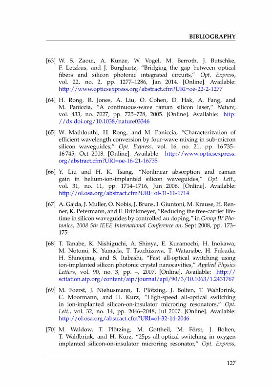
BIBLIOGRAPHY
[63] W. S. Zaoui, A. Kunze, W. Vogel, M. Berroth, J. Butschke,F. Letzkus, and J. Burghartz, “Bridging the gap between opticalfibers and silicon photonic integrated circuits,” Opt. Express,vol. 22, no. 2, pp. 1277–1286, Jan 2014. [Online]. Available:http://www.opticsexpress.org/abstract.cfm?URI=oe-22-2-1277
[64] H. Rong, R. Jones, A. Liu, O. Cohen, D. Hak, A. Fang, andM. Paniccia, “A continuous-wave raman silicon laser,” Nature,vol. 433, no. 7027, pp. 725–728, 2005. [Online]. Available: http://dx.doi.org/10.1038/nature03346
[65] W. Mathlouthi, H. Rong, and M. Paniccia, “Characterization ofefficient wavelength conversion by four-wave mixing in sub-micronsilicon waveguides,” Opt. Express, vol. 16, no. 21, pp. 16 735–16 745, Oct 2008. [Online]. Available: http://www.opticsexpress.org/abstract.cfm?URI=oe-16-21-16735
[66] Y. Liu and H. K. Tsang, “Nonlinear absorption and ramangain in helium-ion-implanted silicon waveguides,” Opt. Lett.,vol. 31, no. 11, pp. 1714–1716, Jun 2006. [Online]. Available:http://ol.osa.org/abstract.cfm?URI=ol-31-11-1714
[67] A. Gajda, J. Muller, O. Nobis, J. Bruns, I. Giuntoni, M. Krause, H. Ren-ner, K. Petermann, and E. Brinkmeyer, “Reducing the free-carrier life-time in silicon waveguides by controlled au doping,” in Group IV Pho-tonics, 2008 5th IEEE International Conference on, Sept 2008, pp. 173–175.
[68] T. Tanabe, K. Nishiguchi, A. Shinya, E. Kuramochi, H. Inokawa,M. Notomi, K. Yamada, T. Tsuchizawa, T. Watanabe, H. Fukuda,H. Shinojima, and S. Itabashi, “Fast all-optical switching usingion-implanted silicon photonic crystal nanocavities,” Applied PhysicsLetters, vol. 90, no. 3, pp. –, 2007. [Online]. Available: http://scitation.aip.org/content/aip/journal/apl/90/3/10.1063/1.2431767
[69] M. Foerst, J. Niehusmann, T. Plotzing, J. Bolten, T. Wahlbrink,C. Moormann, and H. Kurz, “High-speed all-optical switchingin ion-implanted silicon-on-insulator microring resonators,” Opt.Lett., vol. 32, no. 14, pp. 2046–2048, Jul 2007. [Online]. Available:http://ol.osa.org/abstract.cfm?URI=ol-32-14-2046
[70] M. Waldow, T. Plotzing, M. Gottheil, M. Forst, J. Bolten,T. Wahlbrink, and H. Kurz, “25ps all-optical switching in oxygenimplanted silicon-on-insulator microring resonator,” Opt. Express,
127
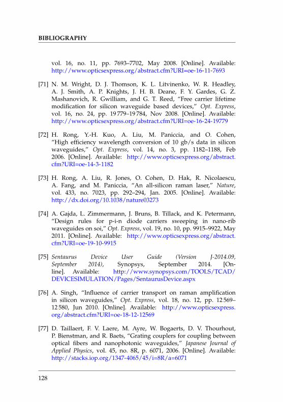
BIBLIOGRAPHY
vol. 16, no. 11, pp. 7693–7702, May 2008. [Online]. Available:http://www.opticsexpress.org/abstract.cfm?URI=oe-16-11-7693
[71] N. M. Wright, D. J. Thomson, K. L. Litvinenko, W. R. Headley,A. J. Smith, A. P. Knights, J. H. B. Deane, F. Y. Gardes, G. Z.Mashanovich, R. Gwilliam, and G. T. Reed, “Free carrier lifetimemodification for silicon waveguide based devices,” Opt. Express,vol. 16, no. 24, pp. 19 779–19 784, Nov 2008. [Online]. Available:http://www.opticsexpress.org/abstract.cfm?URI=oe-16-24-19779
[72] H. Rong, Y.-H. Kuo, A. Liu, M. Paniccia, and O. Cohen,“High efficiency wavelength conversion of 10 gb/s data in siliconwaveguides,” Opt. Express, vol. 14, no. 3, pp. 1182–1188, Feb2006. [Online]. Available: http://www.opticsexpress.org/abstract.cfm?URI=oe-14-3-1182
[73] H. Rong, A. Liu, R. Jones, O. Cohen, D. Hak, R. Nicolaescu,A. Fang, and M. Paniccia, “An all-silicon raman laser,” Nature,vol. 433, no. 7023, pp. 292–294, Jan. 2005. [Online]. Available:http://dx.doi.org/10.1038/nature03273
[74] A. Gajda, L. Zimmermann, J. Bruns, B. Tillack, and K. Petermann,“Design rules for p-i-n diode carriers sweeping in nano-ribwaveguides on soi,” Opt. Express, vol. 19, no. 10, pp. 9915–9922, May2011. [Online]. Available: http://www.opticsexpress.org/abstract.cfm?URI=oe-19-10-9915
[75] Sentaurus Device User Guide (Version J-2014.09,September 2014), Synopsys, September 2014. [On-line]. Available: http://www.synopsys.com/TOOLS/TCAD/DEVICESIMULATION/Pages/SentaurusDevice.aspx
[76] A. Singh, “Influence of carrier transport on raman amplificationin silicon waveguides,” Opt. Express, vol. 18, no. 12, pp. 12 569–12 580, Jun 2010. [Online]. Available: http://www.opticsexpress.org/abstract.cfm?URI=oe-18-12-12569
[77] D. Taillaert, F. V. Laere, M. Ayre, W. Bogaerts, D. V. Thourhout,P. Bienstman, and R. Baets, “Grating couplers for coupling betweenoptical fibers and nanophotonic waveguides,” Japanese Journal ofApplied Physics, vol. 45, no. 8R, p. 6071, 2006. [Online]. Available:http://stacks.iop.org/1347-4065/45/i=8R/a=6071
128
BIBLIOGRAPHY
[78] H. Tian, G. Winzer, A. Gajda, K. Petermann, B. Tillack, andL. Zimmermann, “Fabrication of low-loss soi nano-waveguidesincluding beol processes for nonlinear applications,” Journal ofthe European Optical Society - Rapid publications, vol. 7, no. 0,2012. [Online]. Available: http://www.jeos.org/index.php/jeos rp/article/view/12032
[79] T. K. Liang, H. K. Tsang, I. E. Day, J. Drake, A. P. Knights, andM. Asghari, “Silicon waveguide two-photon absorption detectorat 1.5 µm wavelength for autocorrelation measurements,” AppliedPhysics Letters, vol. 81, no. 7, pp. 1323–1325, 2002. [Online].Available: http://scitation.aip.org/content/aip/journal/apl/81/7/10.1063/1.1500430
[80] L. Alloatti, C. Koos, and J. Leuthold, “Optical loss by surface transferdoping in silicon waveguides,” ArXiv e-prints, Apr. 2015. [Online].Available: http://arxiv.org/abs/1504.07613v1
[81] B. J. Soller, D. K. Gifford, M. S. Wolfe, and M. E. Frog-gatt, “High resolution optical frequency domain reflectometryfor characterization of components and assemblies,” Opt. Ex-press, vol. 13, no. 2, pp. 666–674, Jan 2005. [Online]. Available:http://www.opticsexpress.org/abstract.cfm?URI=oe-13-2-666
[82] R. Duncan, B. Soller, D. Gifford, S. Kreger, R. Seeley,A. Sang, M. Wolfe, and M. Froggatt, “Ofdr-based distributedsensing and fault detection for single-and multi-mode avion-ics fiber-optics,” in Joint Conf. on Aging Aircraft, 2007. [On-line]. Available: http://lunainc.com/wp-content/uploads/2012/08/OFDR-Based-Distributed-Sensing.pdf
[83] R. Claps, D. Dimitropoulos, V. Raghunathan, Y. Han, andB. Jalali, “Observation of stimulated raman amplification in siliconwaveguides,” Opt. Express, vol. 11, no. 15, pp. 1731–1739, Jul2003. [Online]. Available: http://www.opticsexpress.org/abstract.cfm?URI=oe-11-15-1731
[84] R. Slavik, F. Parmigiani, J. Kakande, C. Lundstroem, M. Sjoedin,P. Andrekson, R. Weerasuriya, S. Sygletos, A. D. Ellis, L. Gruener-Nielsen, D. Jakobsen, S. Herstroem, R. Phelan, J. O’Gorman, A. Bo-gris, D. Syvridis, S. Dasgupta, P. Petropoulos, and D. J. Richardson,“All-optical phase and amplitude regenerator for next-generation
129
BIBLIOGRAPHY
telecommunications systems,” Nature Photonics, vol. 4, pp. 690–695,2010.
[85] P. Dumon, G. Priem, L. R. Nunes, W. Bogaerts, D. V. Thourhout,P. Bienstman, T. K. Liang, M. Tsuchiya, P. Jaenen, S. Beckx,J. Wouters, and R. Baets, “Linear and nonlinear nanophotonicdevices based on silicon-on-insulator wire waveguides,” JapaneseJournal of Applied Physics, vol. 45, no. 8S, p. 6589, 2006. [Online].Available: http://stacks.iop.org/1347-4065/45/i=8S/a=6589
[86] Q. Lin, J. Zhang, G. Piredda, R. W. Boyd, P. M. Fauchet, and G. P.Agrawal, “Dispersion of silicon nonlinearities in the near infraredregion,” Applied Physics Letters, vol. 91, no. 2, pp. –, 2007. [Online].Available: http://scitation.aip.org/content/aip/journal/apl/91/2/10.1063/1.2750523
[87] Q. Lin, J. Zhang, P. M. Fauchet, and G. P. Agrawal,“Ultrabroadband parametric generation and wavelength con-version in silicon waveguides,” Opt. Express, vol. 14,no. 11, pp. 4786–4799, May 2006. [Online]. Available:http://www.opticsexpress.org/abstract.cfm?URI=oe-14-11-4786
[88] I.-W. Hsieh, X. Chen, J. I. Dadap, N. C. Panoiu, J. RichardM. Osgood, S. J. McNab, and Y. A. Vlasov, “Cross-phasemodulation-induced spectral and temporal effects on co-propagatingfemtosecond pulses in silicon photonic wires,” Opt. Express,vol. 15, no. 3, pp. 1135–1146, Feb 2007. [Online]. Available:http://www.opticsexpress.org/abstract.cfm?URI=oe-15-3-1135
[89] B. Kuyken, X. Liu, R. M. O. Jr., R. Baets, G. Roelkens, and W. M. J.Green, “Mid-infrared to telecom-band supercontinuum generation inhighly nonlinear silicon-on-insulator wire waveguides,” Opt. Express,vol. 19, no. 21, pp. 20 172–20 181, Oct 2011. [Online]. Available:http://www.opticsexpress.org/abstract.cfm?URI=oe-19-21-20172
[90] X. Liu, R. M. Osgood, Y. A. Vlasov, and W. M. J. Green, “Mid-infrared optical parametric amplifier using silicon nanophotonicwaveguides,” Nature Photon, vol. 4, no. 8, pp. 557–560, Aug 2010.[Online]. Available: http://dx.doi.org/10.1038/NPHOTON.2010.119
[91] S. Zlatanovic, J. Park, F. Gholami, J. Boggio, S. Moro, N. Alic,S. Mookherjea, and S. Radic, “Mid-infrared wavelength conversionin silicon waveguides pumped by silica-fiber-based source,” Selected
130

BIBLIOGRAPHY
Topics in Quantum Electronics, IEEE Journal of, vol. 18, no. 2, pp. 612–620, March 2012.
131
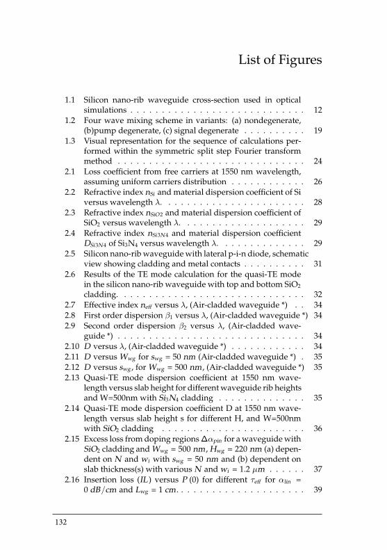
List of Figures
1.1 Silicon nano-rib waveguide cross-section used in opticalsimulations . . . . . . . . . . . . . . . . . . . . . . . . . . . . 12
1.2 Four wave mixing scheme in variants: (a) nondegenerate,(b)pump degenerate, (c) signal degenerate . . . . . . . . . . 19
1.3 Visual representation for the sequence of calculations per-formed within the symmetric split step Fourier transformmethod . . . . . . . . . . . . . . . . . . . . . . . . . . . . . . 24
2.1 Loss coefficient from free carriers at 1550 nm wavelength,assuming uniform carriers distribution . . . . . . . . . . . . 26
2.2 Refractive index nSi and material dispersion coefficient of Siversus wavelength λ. . . . . . . . . . . . . . . . . . . . . . . 28
2.3 Refractive index nSiO2 and material dispersion coefficient ofSiO2 versus wavelength λ. . . . . . . . . . . . . . . . . . . . 29
2.4 Refractive index nSi3N4 and material dispersion coefficientDSi3N4 of Si3N4 versus wavelength λ. . . . . . . . . . . . . . 29
2.5 Silicon nano-rib waveguide with lateral p-i-n diode, schematicview showing cladding and metal contacts . . . . . . . . . . 31
2.6 Results of the TE mode calculation for the quasi-TE modein the silicon nano-rib waveguide with top and bottom SiO2
cladding. . . . . . . . . . . . . . . . . . . . . . . . . . . . . . 322.7 Effective index neff versus λ, (Air-cladded waveguide *) . . 342.8 First order dispersion β1 versus λ, (Air-cladded waveguide *) 342.9 Second order dispersion β2 versus λ, (Air-cladded wave-
guide *) . . . . . . . . . . . . . . . . . . . . . . . . . . . . . . 342.10 D versus λ, (Air-cladded waveguide *) . . . . . . . . . . . . 342.11 D versus Wwg for swg = 50 nm (Air-cladded waveguide *) . 352.12 D versus swg , for Wwg = 500 nm , (Air-cladded waveguide *) 352.13 Quasi-TE mode dispersion coefficient at 1550 nm wave-
length versus slab height for different waveguide rib heightsand W=500nm with Si3N4 cladding . . . . . . . . . . . . . . 35
2.14 Quasi-TE mode dispersion coefficient D at 1550 nm wave-length versus slab height s for different H, and W=500nmwith SiO2 cladding . . . . . . . . . . . . . . . . . . . . . . . 36
2.15 Excess loss from doping regions ∆αpin for a waveguide withSiO2 cladding and Wwg = 500 nm , Hwg = 220 nm (a) depen-dent on N and wi with swg = 50 nm and (b) dependent onslab thickness(s) with various N and wi = 1.2 µm . . . . . . 37
2.16 Insertion loss (IL ) versus P (0) for different τeff for αlin =0 dB/cm and Lwg = 1 cm . . . . . . . . . . . . . . . . . . . . . 39
132
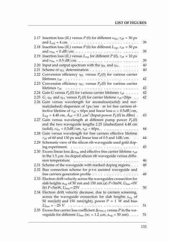
LIST OF FIGURES
2.17 Insertion loss (IL ) versus P (0) for different αlin , τeff = 50 psand Lwg = 4 cm . . . . . . . . . . . . . . . . . . . . . . . . . . 39
2.18 Insertion loss (IL ) versus P (0) for different Lwg , τeff = 50 psand αlin = 0 dB/cm . . . . . . . . . . . . . . . . . . . . . . . . 39
2.19 Insertion loss (IL ) versus Lwg for different P (0), τeff = 10 psand αlin = 0.5 dB/cm . . . . . . . . . . . . . . . . . . . . . . . 39
2.20 Input and output spectrum with the η0L and ηLL . . . . . . . 402.21 Scheme of ηLL determination . . . . . . . . . . . . . . . . . . 402.22 Conversion efficiency η0L versus Pp (0) for various carrier
lifetimes τeff . . . . . . . . . . . . . . . . . . . . . . . . . . . 422.23 Conversion efficiency ηLL versus Pp (0) for various carrier
lifetimes τeff . . . . . . . . . . . . . . . . . . . . . . . . . . . 422.24 Gain G versus Pp (0) for various carrier lifetimes τeff . . . . . 422.25 G , η0L and ηLL versus Pp (0) for carrier lifetime τeff =20ps . . 422.26 Gain versus wavelength for anomalous(solid) and nor-
mal(dashed) dispersion of 1ps/nm · m for free carriers ef-fective lifetime of τeff = 60ps and linear loss α = 0.5dB/cm ,Lwg = 4.48 cm , Aeff = 0.1 µm2.(Input power Pp (0) in dBm) . 43
2.27 Gain versus wavelength at different pump power Pp (0)and the two waveguide lengths 2.25 (dashed)and 4.48 cm(solid), αlin = 0.5dB/cm , τeff = 60ps . . . . . . . . . . . . . . . 44
2.28 Gain versus wavelength for free carriers effective lifetimeτeff of 60 and 130 ps and linear loss of 0.5 and 1dB/cm. . . 44
2.29 Schematic view of the silicon rib waveguide used gold dop-ing experiment. . . . . . . . . . . . . . . . . . . . . . . . . . 45
2.30 Excess linear loss ∆αlin and effective free carrier lifetime τeff
in the 1.5 µm Au doped silicon rib waveguide versus diffu-sion temperature. . . . . . . . . . . . . . . . . . . . . . . . . 46
2.31 Scheme of the waveguide with marked doping regions . . . 482.32 Bias connection scheme for p-i-n assisted waveguide and
free carriers generation profile . . . . . . . . . . . . . . . . . 482.33 Electron drift velocity across the waveguides crossection for
slab heights swg of 50 nm and 150 nm .(a) P=5mW, Ubias =0V(b) P=5mW, Ubias =-25V . . . . . . . . . . . . . . . . . . . . . 50
2.34 Electron drift velocity decrease, due to carriers screening,across the waveguide crossection for slab heights swg of50 nm(left) and 150 nm(right), power P = 1 W and biasUbias = −25 V . . . . . . . . . . . . . . . . . . . . . . . . . . . 51
2.35 Excess free carrier loss coefficient ∆αFCA versus P in the wa-veguide for different Ubias (wi = 1.2 µm , swg = 50 nm). . . . 51
133
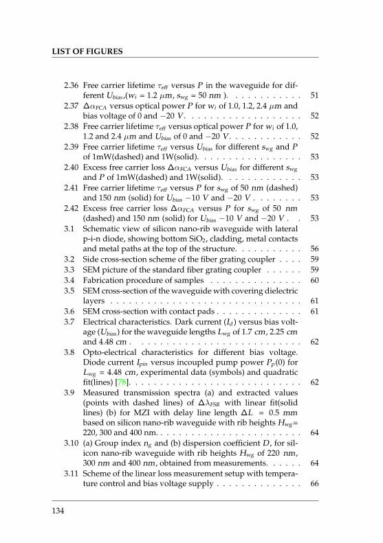
LIST OF FIGURES
2.36 Free carrier lifetime τeff versus P in the waveguide for dif-ferent Ubias ,(wi = 1.2 µm , swg = 50 nm ). . . . . . . . . . . . 51
2.37 ∆αFCA versus optical power P for wi of 1.0, 1.2, 2.4 µm andbias voltage of 0 and −20 V . . . . . . . . . . . . . . . . . . . 52
2.38 Free carrier lifetime τeff versus optical power P for wi of 1.0,1.2 and 2.4 µm and Ubias of 0 and −20 V . . . . . . . . . . . . 52
2.39 Free carrier lifetime τeff versus Ubias for different swg and Pof 1mW(dashed) and 1W(solid). . . . . . . . . . . . . . . . . 53
2.40 Excess free carrier loss ∆αFCA versus Ubias for different swg
and P of 1mW(dashed) and 1W(solid). . . . . . . . . . . . . 532.41 Free carrier lifetime τeff versus P for swg of 50 nm (dashed)
and 150 nm (solid) for Ubias −10 V and −20 V . . . . . . . . 532.42 Excess free carrier loss ∆αFCA versus P for swg of 50 nm
(dashed) and 150 nm (solid) for Ubias −10 V and −20 V . . 533.1 Schematic view of silicon nano-rib waveguide with lateral
p-i-n diode, showing bottom SiO2, cladding, metal contactsand metal paths at the top of the structure. . . . . . . . . . . 56
3.2 Side cross-section scheme of the fiber grating coupler . . . . 593.3 SEM picture of the standard fiber grating coupler . . . . . . 593.4 Fabrication procedure of samples . . . . . . . . . . . . . . . 603.5 SEM cross-section of the waveguide with covering dielectric
layers . . . . . . . . . . . . . . . . . . . . . . . . . . . . . . . 613.6 SEM cross-section with contact pads . . . . . . . . . . . . . . 613.7 Electrical characteristics. Dark current (Id ) versus bias volt-
age (Ubias ) for the waveguide lengths Lwg of 1.7 cm , 2.25 cmand 4.48 cm . . . . . . . . . . . . . . . . . . . . . . . . . . . 62
3.8 Opto-electrical characteristics for different bias voltage.Diode current Ipin versus incoupled pump power Pp (0) forLwg = 4.48 cm , experimental data (symbols) and quadraticfit(lines) [78]. . . . . . . . . . . . . . . . . . . . . . . . . . . . 62
3.9 Measured transmission spectra (a) and extracted values(points with dashed lines) of ∆λFSR with linear fit(solidlines) (b) for MZI with delay line length ∆L = 0.5 mmbased on silicon nano-rib waveguide with rib heights Hwg =220, 300 and 400 nm. . . . . . . . . . . . . . . . . . . . . . . . 64
3.10 (a) Group index ng and (b) dispersion coefficient D , for sil-icon nano-rib waveguide with rib heights Hwg of 220 nm ,300 nm and 400 nm , obtained from measurements. . . . . . 64
3.11 Scheme of the linear loss measurement setup with tempera-ture control and bias voltage supply . . . . . . . . . . . . . . 66
134
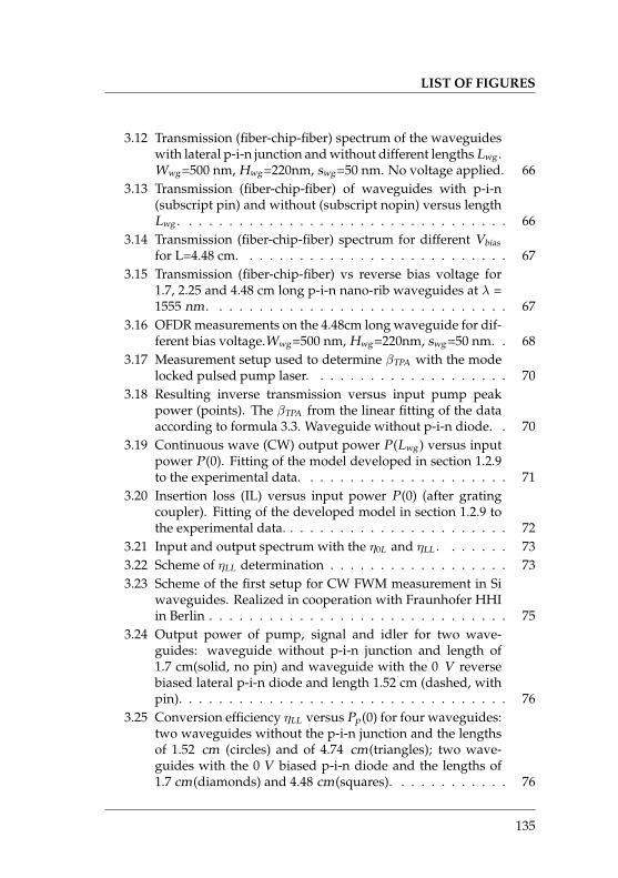
LIST OF FIGURES
3.12 Transmission (fiber-chip-fiber) spectrum of the waveguideswith lateral p-i-n junction and without different lengths Lwg .Wwg =500 nm, Hwg =220nm, swg =50 nm. No voltage applied. 66
3.13 Transmission (fiber-chip-fiber) of waveguides with p-i-n(subscript pin) and without (subscript nopin) versus lengthLwg . . . . . . . . . . . . . . . . . . . . . . . . . . . . . . . . . 66
3.14 Transmission (fiber-chip-fiber) spectrum for different Vbias
for L=4.48 cm. . . . . . . . . . . . . . . . . . . . . . . . . . . 673.15 Transmission (fiber-chip-fiber) vs reverse bias voltage for
1.7, 2.25 and 4.48 cm long p-i-n nano-rib waveguides at λ =1555 nm . . . . . . . . . . . . . . . . . . . . . . . . . . . . . . 67
3.16 OFDR measurements on the 4.48cm long waveguide for dif-ferent bias voltage.Wwg =500 nm, Hwg =220nm, swg =50 nm. . 68
3.17 Measurement setup used to determine βTPA with the modelocked pulsed pump laser. . . . . . . . . . . . . . . . . . . . 70
3.18 Resulting inverse transmission versus input pump peakpower (points). The βTPA from the linear fitting of the dataaccording to formula 3.3. Waveguide without p-i-n diode. . 70
3.19 Continuous wave (CW) output power P (Lwg ) versus inputpower P (0). Fitting of the model developed in section 1.2.9to the experimental data. . . . . . . . . . . . . . . . . . . . . 71
3.20 Insertion loss (IL) versus input power P (0) (after gratingcoupler). Fitting of the developed model in section 1.2.9 tothe experimental data. . . . . . . . . . . . . . . . . . . . . . . 72
3.21 Input and output spectrum with the η0L and ηLL . . . . . . . 733.22 Scheme of ηLL determination . . . . . . . . . . . . . . . . . . 733.23 Scheme of the first setup for CW FWM measurement in Si
waveguides. Realized in cooperation with Fraunhofer HHIin Berlin . . . . . . . . . . . . . . . . . . . . . . . . . . . . . . 75
3.24 Output power of pump, signal and idler for two wave-guides: waveguide without p-i-n junction and length of1.7 cm(solid, no pin) and waveguide with the 0 V reversebiased lateral p-i-n diode and length 1.52 cm (dashed, withpin). . . . . . . . . . . . . . . . . . . . . . . . . . . . . . . . . 76
3.25 Conversion efficiency ηLL versus Pp (0) for four waveguides:two waveguides without the p-i-n junction and the lengthsof 1.52 cm (circles) and of 4.74 cm(triangles); two wave-guides with the 0 V biased p-i-n diode and the lengths of1.7 cm(diamonds) and 4.48 cm(squares). . . . . . . . . . . . 76
135
LIST OF FIGURES
3.26 Conversion efficiency ηLL for Lwg of1.7 cm , 2.25 cm and4.48 cm , Pp (0) = 26dBm , λp = 1552.5nm , λs = 1550nm . . . 77
3.27 Conversion efficiency ηLL for three pump wavelengths ver-sus signal detuning ∆λ. Pp (0) = 26 dBm , Lwg = 4.48 cm ,Ubias = 30 V . . . . . . . . . . . . . . . . . . . . . . . . . . . . 77
3.28 Output spectrum recorded by OSA for the waveguide oflength Lwg = 4.48 cm, Pp (0) = 26.5dBm , λp = 1552.5 nm ,λs = 1550 nm , Ubias = −20 V . . . . . . . . . . . . . . . . . 78
3.29 Dependence of the ηLL on Pp (0) for several reverse Ubias val-ues, λp = 1552.5 nm , λs = 1550 nm , Lwg = 4.48 cm .. . . . . . . . . . . . . . . . . . . . . . . . . . . . . . . . . . . 78
3.30 Comparison of ηLL relation to incoupled pump power Pp (0)for 2.25 cm and 4.48 cm long waveguide for three bias volt-age levels. λp = 1552.5nm , λs = 1550nm . . . . . . . . . . . . 79
3.31 Second measurement setup for CW FWM measurement inSi waveguides. Realized in cooperation with the group atDTU. . . . . . . . . . . . . . . . . . . . . . . . . . . . . . . . 80
3.32 Measured power of signal at input Ps (0) and output Ps (Lwg )and Pi (Lwg ) idler versus wavelength of the input signal λs
for Pp (0) = 21.5 dBm . The input signal was always thesame, thus the signal curves overlap. . . . . . . . . . . . . . 81
3.33 Measured conversion efficiency η0L (solid) and ηLL (dashed)versus wavelength of the input signal λs for waveguidelengths 1.7 cm, 2.25 cm, 4.48 cm, pump wavelength λp =1552 nmand Pp (0) = 21.5dBm , Ubias = 0V . . . . . . . . . . . . . . . . 83
3.34 Measured conversion efficiency η0L versus wavelength ofthe input signal λs , for waveguide lengths 1.7 cm, 2.25 cm,4.48 cm, pump wavelength λp =1552 nm and Pp (0) = 21.5dBm ,Ubias = 28.2V . . . . . . . . . . . . . . . . . . . . . . . . . . . . 83
3.35 Measured conversion efficiency ηLL versus wavelength ofthe input signal λs , for waveguide lengths 1.7 cm, 2.25 cmand 4.48 cm, pump wavelength λp =1552 nm and Pp (0) =21.5dBm , reverse Ubias = 28.2V . . . . . . . . . . . . . . . . . 84
3.36 Experimentally determined ηLL versus λs variable Ubias (symbols)L = 4.48 cm, pump power Pp (0)=21.5dBm, and correspond-ing numerically determined characteristics for differentfree carrier lifetimes (solid curves). (Fit parameters γ =280 [1/(W · m)], βTPA = 5.6 · 10−10cm/W , Aeff = 0.1 µm2,αlin = 1.2 dB/cm) . . . . . . . . . . . . . . . . . . . . . . . . 84
136
LIST OF FIGURES
3.37 Experimentally determined η0L versus λs variable Ubias
(symbols) L = 4.48 cm, pump power Pp (0)=21.5dBm, andcorresponding simulated characteristics for different life-times (solid curves). (Fit parameters γ = 280 [1/(W · m)],βTPA = 5.6 ·10−10cm/W , Aeff = 0.1 µm2, αlin = 1.2 dB/cm ,D = −1.9ps/ (nm·) . . . . . . . . . . . . . . . . . . . . . . . 85
3.38 Measured nonlinear transmission G as a function of λs forvariable Ubias (symbols) Lwg = 4.48 cm , pump powerPp (0)=21.5dBm, and corresponding simulated characteris-tics for different effective lifetimes τeff (solid curves). Lineartransmission curve (at Ubias = −20V ) was inserted (dashed)to indicate gain. (Fit parameters γ = 280 [1/(W · m)],βTPA = 5.6 ·10−10cm/W , Aeff = 0.1 µm2, αlin = 1.2 dB/cm ,D = −1.9ps/ (nm · m) ) . . . . . . . . . . . . . . . . . . . . . 85
3.39 Conversion efficiency ηLL versus λs for various pump powerPp (0), length Lwg =4.48 cm, Ubias =-28.2 V. Comparison ofthe experimental data(points) to the numerically obtainedcurves (solid line) for the same optical power. (Fit param-eters γ = 280 [1/(W · m)], Aeff = 0.1 µm2, τeff = 130 ps),D = −1.9ps/ (nm · m) ) . . . . . . . . . . . . . . . . . . . . . 87
3.40 Measurement setup used to determine the phase sensitivegain in silicon waveguide . . . . . . . . . . . . . . . . . . . . 88
3.41 Spectra recorded at the input and output of the 4.48 cm longwaveguide for maximum and minimum gain. The totalpower from two pumps P p1(0) + P p2(0) = 19.5dBm . . . . . 89
3.42 Phase sensitive amplification in 1.7, 2.25 and 4.48 cm long p-i-n diode waveguides and the reference waveguide withoutp-i-n diode with length of 4.74 cm. Total pump power 19.5dBm . . . . . . . . . . . . . . . . . . . . . . . . . . . . . . . . 90
3.43 Phase sensitive amplification as a function of phase shift fordifferent total pumps power after the grating coupler andbias of Ubias = -20 V. For the highest power voltage was in-creased to Ubias = -25 V. Lwg =4.48 cm. . . . . . . . . . . . . . 90
4.1 Measurement setup for the wavelength conversion of the40 Gbps NRZ-OOK modulated signal in silicon waveguidewith the lateral p-i-n diode. [43] . . . . . . . . . . . . . . . . 94
4.2 Input(black) and output spectra for the waveguides withoutand with the p-i-n junction. Observed ηLL values for thereference waveguide, 0V and 20V biased p-i-n waveguidewere -26.9 dB, -8 and -4.6 dB respectively. . . . . . . . . . . . 95
137
LIST OF FIGURES
4.3 Measured BER versus received power: back-to-back, outputsignal and idler at -20 V reverse bias voltage and idler at 0 Vbias voltage. The insets show the eye diagrams for the idlerat -20 V bias voltage (A), at 0 V bias voltage(B) and for thewaveguide without junction (C) . . . . . . . . . . . . . . . . 96
4.4 Experimental setup for dynamic phase regeneration of a10 Gbps DPSK signal. . . . . . . . . . . . . . . . . . . . . . . 98
4.5 Optical spectra measured at the input and output of the wa-veguide under dynamic operation with the 10 Gbps signal.. . . . . . . . . . . . . . . . . . . . . . . . . . . . . . . . . . . 99
4.6 Eyes diagrams at the receiver for -36 dBm of received powerbefore(left) and after(right) regeneration, without(top) andwith(bottom) phase noise generated by a 5 GHz tone with amodulation index of 0.57. . . . . . . . . . . . . . . . . . . . . 99
4.7 BER as a function of the received power for different phasenoise loading conditions before (solid symbols) and after(hollow symbols) regeneration. Modulation index of 0.57was used. . . . . . . . . . . . . . . . . . . . . . . . . . . . . . 100
4.8 Power penalty (compared to back-to-back for a BER=10−9)as a function of the modulation index of the 5-GHz radiofrequency tone used to emulate the phase noise . . . . . . . 100
138
List of Publications
[1] F. DaRos, D. Vukovic, A. Gajda, L. Zimmermann, K. Petermann, andC. Peucheret. Continuous wave phase-sensitive four-wave mixingin silicon waveguides with reverse-biased p-i-n junctions. In OpticalCommunication (ECOC 2013), 39th European Conference and Exhibitionon, pages 1–3, Sept 2013.
[2] Francesco DaRos, Dragana Vukovic, Andrzej Gajda, Kjeld Dalgaard,Lars Zimmermann, Bernd Tillack, Michael Galili, Klaus Petermann,and Christophe Peucheret. Phase regeneration of dpsk signals in asilicon waveguide with reverse-biased p-i-n junction. Opt. Express,22(5):5029–5036, Mar 2014.
[3] G. Dziallas, M. Jazajerifar, A. Gajda, L. Zimmermann, and K. Peter-mann. A numerical investigation of continuous wave parametric gainin silicon nano waveguides at wavelengths around 1550 nm. In Nu-merical Simulation of Optoelectronic Devices (NUSOD), 2014 14th Inter-national Conference on, Sept 2014.
[4] A. Gajda, F. Da Ros, D. Vukovic, L. Zimmermann, C. Peucheret,B. Tillack, and K. Peterman. High efficiency wavelength conversionof 40 gbps signals at 1550 nm in soi nano-rib waveguides using p-i-n diodes. In Group IV Photonics (GFP), 2013 IEEE 10th InternationalConference on, pages 160–161, Aug 2013.
[5] A. Gajda, J. Muller, O. Nobis, J. Bruns, I. Giuntoni, M. Krause, H. Ren-ner, K. Petermann, and E. Brinkmeyer. Reducing the free-carrier life-time in silicon waveguides by controlled au doping. In Group IV Pho-tonics, 2008 5th IEEE International Conference on, pages 173–175, Sept2008.
[6] A. Gajda, G. Winzer, B. Tillack, K. Petermann, L. Zimmermann,H. Tian, R. Elschner, T. Richter, and C. Schubert. High efficiency cwfour-wave mixing at 1.5 µm in soi nano-rib waveguides using p-i-ndiodes. In Group IV Photonics (GFP), 2012 IEEE 9th International Con-ference on, pages 225–227, Aug 2012.
[7] Andrzej Gajda, Lars Zimmermann, J. Bruns, B. Tillack, and K. Pe-termann. Design rules for p-i-n diode carriers sweeping in nano-ribwaveguides on soi. Opt. Express, 19(10):9915–9922, May 2011.
[8] Andrzej Gajda, Lars Zimmermann, Mahmoud Jazayerifar, GeorgWinzer, Hui Tian, Robert Elschner, Thomas Richter, Colja Schubert,
139

LIST OF PUBLICATIONS
Bernd Tillack, and Klaus Petermann. Highly efficient cw paramet-ric conversion at 1550 nm in soi waveguides by reverse biased p-i-njunction. Opt. Express, 20(12):13100–13107, Jun 2012.
[9] K Petermann, A Gajda, G Dziallas, M Jazayerifar, L Zimmermann,B Tillack, F Da Ros, D Vukovic, K Dalgaard, M Galili, and ChristophePeucheret. Phase-sensitive optical processing in silicon waveguides.In Optical Fiber Communication Conference (OFC 2015), volume Tu2F ofOptical Fiber Communication Conference - Chip-scale All-optical Process-ing (2015), page Tu2F.4, Los Angeles, United States, March 2015. OSA(ISBN: 978-1-55752-937-4).
[10] H. Tian, G. Winzer, A. Gajda, K. Petermann, B. Tillack, and L. Zim-mermann. Fabrication of low-loss soi nano-waveguides includingbeol processes for nonlinear applications. Journal of the European Op-tical Society - Rapid publications, 7(0), 2012.
140