Embed Size (px)
Citation preview
Foundries and Design Rules
Instructor S. Demlow ECE 410 January 30, 2012
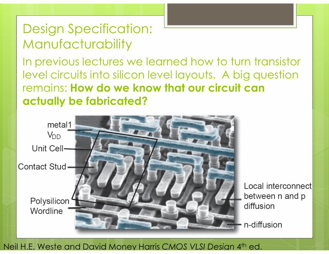
Design Specification: Manufacturability
Neil H.E. Weste and David Money Harris CMOS VLSI Design 4th ed.
In previous lectures we learned how to turn transistor level circuits into silicon level layouts. A big question remains: How do we know that our circuit can actually be fabricated?

Design Rules Each layer is manufactured with specifications on the minimum width, spacing to adjacent layers, overlap over connecting layers, and other geometrical constraints derived from the limits of a specific fabrication process. Some examples:
Neil H.E. Weste and David Money Harris CMOS VLSI Design 4th ed.
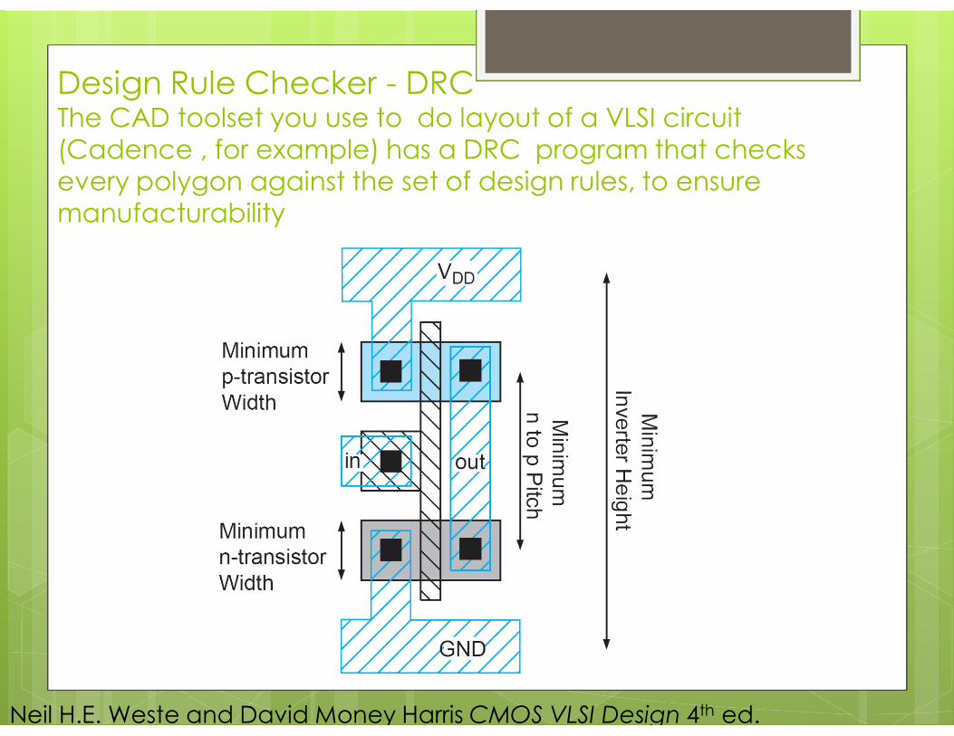
Design Rule Checker - DRC The CAD toolset you use to do layout of a VLSI circuit (Cadence , for example) has a DRC program that checks every polygon against the set of design rules, to ensure manufacturability
Neil H.E. Weste and David Money Harris CMOS VLSI Design 4th ed.
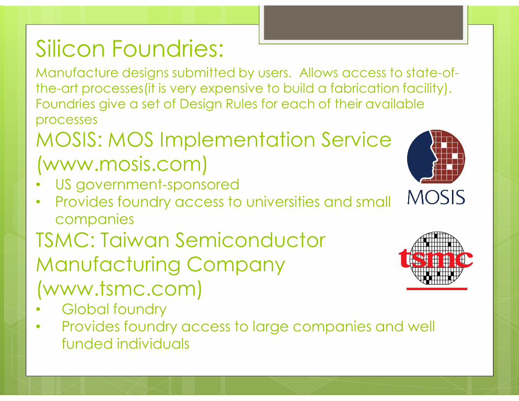
Silicon Foundries: Manufacture designs submitted by users. Allows access to state-of-the-art processes(it is very expensive to build a fabrication facility). Foundries give a set of Design Rules for each of their available processes
MOSIS: MOS Implementation Service (www.mosis.com) • US government-sponsored • Provides foundry access to universities and small
companies TSMC: Taiwan Semiconductor Manufacturing Company (www.tsmc.com) • Global foundry • Provides foundry access to large companies and well
funded individuals
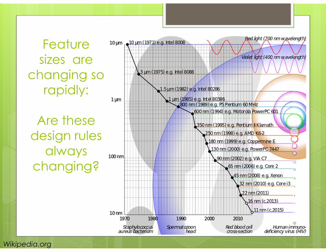
Feature sizes are
changing so rapidly:
Are these
design rules always
changing?
Wikipedia.org
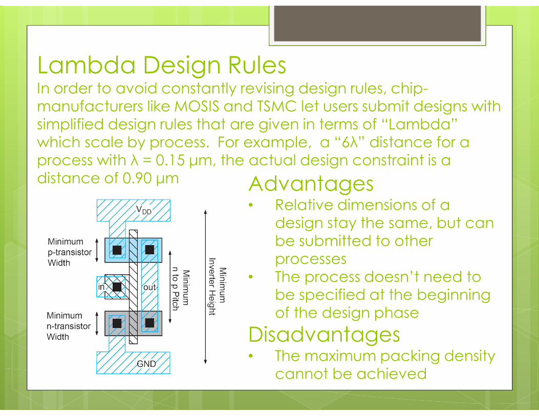
Lambda Design Rules In order to avoid constantly revising design rules, chip-manufacturers like MOSIS and TSMC let users submit designs with simplified design rules that are given in terms of “Lambda” which scale by process. For example, a “6λ” distance for a process with λ = 0.15 μm, the actual design constraint is a distance of 0.90 μm Advantages
• Relative dimensions of a design stay the same, but can be submitted to other processes
• The process doesn’t need to be specified at the beginning of the design phase
Disadvantages • The maximum packing density
cannot be achieved
A look inside an INTEL Fab http://www.youtube.com/watch?v=oMNaBkEIyj0
There are a few other links to good videos about semiconductor processing that you should watch outside of class: Discovery Channel program on how silicon wafers and computer
chips are made. Great footage of silicon wafer growth http://www.youtube.com/watch?v=aWVywhzuHnQ
Current TSMC Fab Technology http://www.youtube.com/watch?v=4Q_n4vdyZzc
Packaging a fabricated INTEL Microprocessor: (Watch from 1:00 – 5:30) http://www.youtube.com/watch?v=Cg-mvrG-K-E&feature=related
Future: 22 nm 3d FETS http://www.youtube.com/watch?v=_zldnUY0t1M&feature=related