Embed Size (px)
Citation preview

LBL - 36166
UC - 426
Paper submitted to the International Conference on Metallurgical Coatings and Thin Films
April 24-28,1995, San Diego, CA ICMCTF-95
Formation of Metal Oxides by Cathodic Arc Deposition
S. Anders, A. Anders, M. Rubin, Z. Wang, S. Raoux, F. Kong, and I. G.
Brown Lawrence Berkeley Laboratory, University of California, Berkeley, CA 94720
March 1995
This work was supported by the U. S. Department of Energy, Division of Advanced Energy
Projects, and the Assistant Secretary for Energy Efficiency and Renewable Energy, Office of
Building Technologies, Building Systems and Materials Division of the U.S. Department of
Energy, under Contract NO. DE-AC03-76SF00098.

DISCLAIMER
This report was prepared as an account of work sponsored by an agency of the United States Government. Neither the United States Government nor any agency thereof, nor any of their employees, make any warranty, express or implied, or assumes any legal liability or responsibility for the accuracy, completeness, or usefulness of any information, apparatus, product, or process disclosed, or represents that its use would not infringe privately owned rights. Reference herein t o any specific commercial product, process, or service by trade name, trademark, manufacturer, or otherwise does not necessarily constitute or imply its endorsement, recommendation, or favoring by the United States Government or any agency thereof. The views and opinions of authors expressed herein do not necessarily state or reflect those of the United States Government or any agency thereof.

DISCLAIMER
Portions of this document may be illegible in electronic image products. Images are produced from the best available original document.

Formation of Metal Oxides by Cathodic Arc Deposition
S. Anders, A. Anders, M. Rubin, 2. Wang, S. Raoux, F. Kong, and I. G. Brown Lawrence Berkeley Laboratory, University of California, Berkeley, CA 94720
Abstract
Metal oxide thin films are of interest for a number of applications. Cathodic arc deposition,
which is an established and industrially applied technique for the formation of nitrides (e.g. TiN),
can also be used for metal oxide thin film fofmation. A cathodic arc plasma source with the desired
cathode material is operated in an oxygen atmosphere of appropriate pressure, and metal oxides of
various stoichiometric composition can be formed on different substrates. We report here on a
series of experiments on metal oxide formation by cathodic arc deposition for different
applications. Black copper oxide has been deposited on accelerator components to increase the
radiative heat transfer between the parts. Various metal oxides such as tungsten oxide, niobium
oxide, nickel oxide and vanadium oxide have been deposited on IT0 glass to form electrochromk
films for window applications. Tantalum oxide films are of interest for replacing polymer
electrolytes. Optical waveguide structures can be formed by refractive index variation using oxide
multilayers. We have synthesized multilayers of A1203lY203/A1203/Si as possible basic
structures for passive optoelectronic integrated circuits, and A12-xErx03 thin films with a variable
Er concentration which is a potential component layer for the production of active optoelectronic
integrated devices such as amplifiers or lasers at a wavelength of 1.53 pm. Aluminum and
1
chromium oxide Nms have been deposited on a number of substrates to impart improved corrosion
resistance at high temperature. Titanium sub-oxides which are electrically conductive and
corrosion resistant and stable in a number of aggressive environments have been deposited on
various substrates. These sub-oxides are of great interest for use in electrochemical cells.
Common features of all these depositions are the high deposition rate typical for cathodic arc
deposition, the good adhesion of the films due to the high metal ion energy, and the advantage of
an environmentally clean method in comparison to wet-chemical oxide formation techniques.
2

1. Introduction
Cathode spots of vacuum arc discharges are sources of highly ionized, dense plasma of the
cathode material. Vacuum arc plasma sources based on this type of discharge have been used to
deposit various metal films, alloy films, and amorphous hard carbon films of high quality, in
particular if the sources are equipped with macroparticle filters to remove the solid debris which is
formed at the cathodes of the sources along with the plasma, If these sources are operated in a
gaseous atmosphere such as nitrogen or oxygen, chemical compounds can be formed. The
cathode spot mechanism is similar, and the sources are then more appropriately called cathodic arc
plasma sources. The formation of nitrides such as, e.g., TiN, HM, ZrN, and also (Ti, A1)N by
cathodic arc deposition is an established technique and has many applications, in particular hard
coatings for tools. The formation of oxides is possible in the same way by operating a cathodic arc
metal plasma source in an oxygen environment [ 1,2]. This technique has a number of advantages
in comparison to other oxide formation techniques. The method is high rate, environmentally
clean, and flexible in the sense that by varying plasma production and gas pressure oxides of
various stoichiometric ratio can be formed. By operating two or more sources Simultaneously or
by using alloy cathodes it is possible to deposit oxides containing more than one metal species. A
further advantage is the possible combination of cathodic arc deposition of oxides with various
biasing techniques of the substrates, which allows one to influence the metal ion energy and
thereby to modify the substrate-film interface and the film properties.
In the present paper we report on experiments which were performed to deposit metal oxides
of various types for a number of applications. We describe the plasma source and macroparticle
filter designs, their application to metal oxide formation, and the properties of the deposited oxide
films.
3

2. Cathodic Arc Plasma Sources and Macroparticle Filters
A variety of cathodic arc plasma sources have been designed and operated depending on the
specific application. Our smallest source has a cathode diameter of 3 mm and is operated in a
pulsed mode (typical pulse length 250 ps, 1-5 Hz); it is suited for the deposition of monolayers up
to films of 10 nm. Our largest source has a cathode diameter of 50 mm, is water-cooled, can
operate continuously, and is designed for the deposition of thick films in the micron range on large
substrates. For high-quality applications, macroparticle-free films are required, and all our sources
can be combined with 90 degrees bent magnetic macroparticle filters of various sizes. For other
applications a slight macroparticle contamination of the films can be tolerated and the sources are
operated without a filter. The sources and/or the substrates can be mounted on moveable
feedthroughs which allows the coating of complex or large substrates. A detailed description of
sources and filters can be found elsewhere [3-71.
We apply a pulse biasing technique for many depositions in order to enhance the adhesion
and to influence the film properties. The substrates which are immersed in the plasma are
repetitively pulse biased to a negative voltage. During the bias pulses ions are extracted from the
plasma, accelerated and implanted into the substrates whereas between the pulses low-energy
deposition takes place. This method is called Plasma Immersion Ion Implantation and Deposition
and is described in detail elsewhere [S, 93.
3. Applications
3.1. Formation of black CuOfilm for increased heat tranqfer
The radiation properties of CuO are close to those of an ideal black body making it a good
coating for applications of enhanced radiation heat transfer. The longitudinal feedback kicker of
the Advanced Light Source at Lawrence Berkeley Laboratory needs additional cooling because the
kicker electrodes are heated by currents induced in the structure by the electron beam; and they
transfer this heat mainly by radiation to the kicker housing. The kicker is made from aluminum
and consists of four RF electrode pairs inside a kicker housing which is a tube of 1 m length and
an inner diameter of 15 cm. A black coating CuO on the kicker surfaces can increase the radiation
heat transfer considerably. Copper oxide was deposited using a cathodic arc plasma source with a
copper cathode (50 mm diameter) operated in an oxygen atmosphere at a pressure of 40 Pa. The
arc current was 120 A, the arc duration 250 ms, and the arc repetition rate 0.5 s-l. For this
particular deposition we used a plasma source without anode and configured the substrate as the
anode for coating the outside of kicker electrodes as well as for coating the inside of the kicker
housing. In this application a slight contamination of the CuO film by macroparticles can be
tolerated as long as the f i i appears black because a few micron-size copper macroparticles do not
influence the RF behavior of the device. The kicker electrodes were mounted on a movable
vacuum feedthrough to allow rotation and longitudinal movement. The inside of the kicker
housing was coated by moving the plasma source through the bore of the housing. Areas which
were not to be coated were covered by stainless steel masks. Figure 1 shows one of the electrodes
and the housing after deposition and removal of the masks. The average deposition rate was
5 nm/s over an area of 100 cm2 for the deposition of the electrodes, and 20 1 4 s over an area of
100 cm2 for the inside of the kicker housing.
The CuO films were characterized by different methods to verify their chemical composition
and structure, adhesion, RF behavior and UHV compatibility. The chemical composition and
thickness of the films was determined by Rutherford Backscattering Spectrometry ( R B S ) . The
films were found to be slightly oxygen-rich with a nominal composition of CuO1.23 and a
thickness of 5 pm. The crystal structure of the films was studied by X-ray diffraction (XRD) in
the Bragg geometry using the Cu K a line (h = 0.154 nm). XRD results show low diffraction
peak intensities of the CuO phase, with broad CuO diffraction peaks indicating that the CuO grain
size in this film is small. Because no diffraction peaks of other copper oxide phases are present, it
is believed that this film is mostly amorphous with some small grains of crystalline CuO.
~
5

Adhesion was tested using a pull tester. The pull strength necessary to remove the CuO films from
the aluminum substrates exceeded 60 MPa which was the internal strength of the epoxy. The
coated kicker parts were vacuum baked twice in a furnace at a temperature of 150°C for 8 hours.
No degradation of the film quality was observed after vacuum baking. The kicker was tested for
RF performance before and after CuO coating, and the transmission loss was identical in both
cases. Impedance measurements from 500 MHz to 26 GHz also showed no significant differences
indicating that the coating is transparent to RF radiation and well suited for coating of RF devices.
Heating tests were performed with CuO-coated aluminum parts which resembled the kicker
geometry. When uncoated, cleaned aluminum parts were used and the temperature of the inner
electrodes increased asymptotically by up to 1WC at a heating power of 8 Watts; this temperature
increase is not acceptable for kicker operation. After CuO coating of the parts the temperature rise
was only 50°C which is a value that can be tolerated during kicker operation. The test
demonstrates the successful enhancement of thermal radiation heat transfer from the inner
electrodes to the outer housing by increased radiation from the black surfaces of the parts. The
kicker was assembled and installed at the Advanced Light Source, and a base pressure of better
than 10-8 Pa has been reached. The experiment is described in detail elsewhere [lo].
3 2 . Formation of electrochromic oxidefilms
Metal oxides are used in various applications for windows such as spectrally selective
coatings and electrochromic windows. Electrochromic windows are multilayer structures of
various types containing different metal oxide layers. A typical electrochromic device consists of a
structure like glass/transparent conductor/cathodic electrochromic electrodebonic conductor/anodic
electrochromic electrode/transparent conductor/glass. Tin oxide or indium tin oxide (ITO) films are
transparent and conducting; and they act as contacts in these structures. Switching elements of the
structures change reversibly from transparent to colored when ions are injected into or extracted
from these films. Some metal oxides such as tungsten oxide, titanium oxide, niobium oxide or
6
vanadium oxide show a cathodic coloration, whereas other oxides such as nickel oxide or cobalt
oxide show anodic coloration. The ion conductors in complete solid state devices are also
relatively thick oxides such as tantalum oxide and lithium niobate.
We have applied the method of cathodic arc deposition to form oxides of tungsten, nickel,
vanadium, niobium, and tantalum thin films on various substrates. Plasma sources with 25 mm
cathode diameter have been operated in pulsed mode with and without macroparticle filters.
Typical arc current was 300 A, arc duration 5 ms, and arc repetition rate 1 s-l. The sources were
operated at oxygen pressures between 4 and 10 Pa. The substrates were glass and ITO-coated
glass. The average deposition rate was 0.1 nds . The substrates were not cooled during the
deposition. The exposure to the plasma lead to a temperature rise of the substrates during
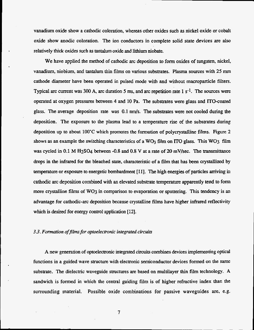
deposition up to about 100°C which promotes the formation of polycrystalline films. Figure 2
shows as an example the switching characteristics of a W03 film on IT0 glass. This W03 film
was cycled in 0.1 M H2SO4 between -0.8 and 0.8 V at a rate of 20 mV/sec. The transmittance
drops in the infrared for the bleached state, characteristic of a film that has been crystallized by
temperature or exposure to energetic bombardment [ 1 I]. The high energies of particles arriving in
cathodic arc deposition combined with an elevated substrate temperature apparently tend to fonn
more crystalline films of W03 in comparison to evaporation or sputtering. This tendency is an
advantage for cathodic-arc deposition because crystalline films have higher infrared reflectivity
which is desired for energy control application [ 121.
3 3 . Formation offilms for optoelectronic integrated circuits
A new generation of optoelectronic integrated circuits combines devices implementing optical
functions in a guided wave structure with electronic semiconductor devices formed on the same
substrate. The dielectric waveguide structures are based on multilayer thin film technology. A
sandwich is formed in which the central guiding film is of higher refractive index than the
surrounding material. Possible oxide combinations for passive waveguides are, e.g.
7

yttridaluminum oxide based structures. The refractive index difference between AI203 and
Y2O3 is high (lo%), and the index profile can be tailored by atomic mixing of Al and Y. Passive
optoelectronic components perform functions like phase matching, wave coupling, deflection,
splitting, filtering, and focusing [13]. By doping the guiding region with optically active
impurities, components such as amplifiers and lasers can be fabricated [14,15]. Depending on the
kind of active impurity, integrated amplifiers and lasers can be generated for a wide range of
wavelengths. An important application is the formation of 1.53 pm lasers by doping the
waveguide with Er ions. This wavelength of 1.53 pm corresponds to the optical window for
minimum loss in silica-based optical fiber transmission.
We have formed A1203 and Y2O3 thin films with appropriate stoichiometric ratio on silicon
substrates by operating filtered aluminum and yttrium sources in an oxygen atmosphere. These
films are the basic elements for passive devices whereas Er-doped aluminum oxide A12-,ErX03
films are required for active elements. Doping of A1203 with erbium was performed in two
different ways. One approach was to use two filtered arc sources (one A1 and one Er source)
directed towards the same substrate which were triggered alternately. The Er concentration was
controlled by setting the pulse lengths of the two sources in the required ratio taking the different
deposition rates of A1 and Er into account. The second approach is the application of an
aluminuderbum compound cathode in a single plasma source.
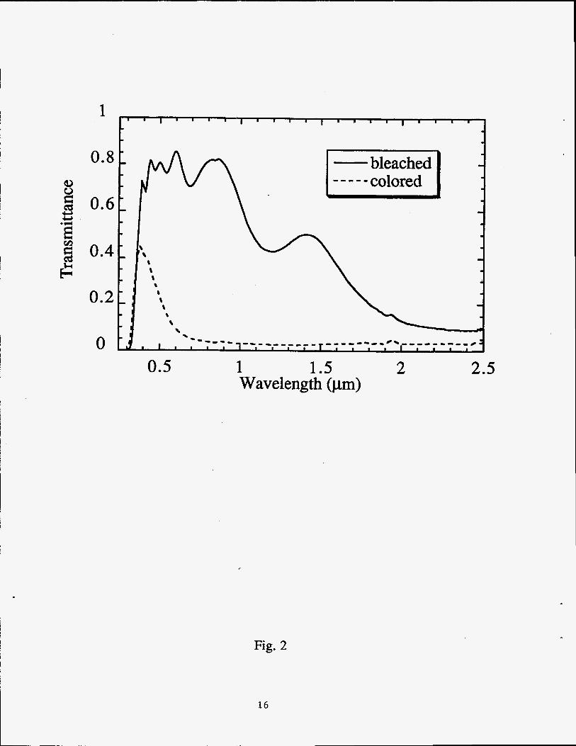
The 1.53 pm emission of erbium originates from the 4113/2-411s/2 intra 4fl1 shell transition of
Er3+ ions. As this orbital is well screened by outer closed shells 5s2 and 5p6 it is relevant to note
that the emission wavelength depends neither on the host matrix nor on its temperature. Due to Er-
Er coupling effects however the concentration of erbium in the material plays an important role. As
the highest concentration of active center must be reached, a balance must be found in dealing with
the excitation efficiency, the cross-relaxation mechanisms, the up-conversion and the self-
quenching phenomena [ 161. Thus the erbium concentration must be optimized. For Er-doped
dielectric materials, this optimum concentration is three orders of magnitude greater than for
erbium-doped classical semiconductors [ 171. In the case of erbium doped aluminum oxide thin
8

films, the concentration of erbium that can be included without reaching the self-quenching
threshold is as high as ~ 4 . 4 5 . Figure 3 shows the photoluminescence spectrum at room
temperature of a 300 nm thick A11.55Er0.4503/Si sample. This film was deposited at room
temperature using two separate Er and AI sources (cathode diameter 6 mm) in an oxygen
atmosphere of 2 Pa. Both sources operated at an arc current of 300 A. The erbium source pulse
duration was 0.5 ms, the aluminum source pulse duration was 5 ms. After deposition the samples
were annealed in air at T==6OO0C for 1 hour.
3.4. Formation of A 1 2 0 3 j T l ~ ~ ~ for improved corrosion resistance at high temperature
Protection from corrosion and environmental effects arising from deleterious reactions with
gases and condensed products is required for advanced high-temperature materials. Stable surface
oxides which are well-adhered to the substrate and retain their mechanical stability after repeated
temperature cycling are desired coatings to protect various materials such as metals, alloys or
compounds.
We have explored the formation of A1203 and Cr2O3 films by cathodic arc deposition on a
variety of substrates such as stainless steel, Sic, and an iron aluminum alloy. The films were
deposited at pressures between 0.5 - 2.5 Pa, a plasma source (cathode diameter 6 nun) with filter
was used at an arc current of 250 A, an arc duration of 5 ms and an arc repetition rate of 1 Hz. A
pulsed bias voltage of -2 kV with a pulse duration of 2 ps and a pulse off-time of 6 ps was applied
to the substrates. The substrates were mounted on a water-cooled sample holder.
As deposited at room temperature, the films are almost amorphous. Figure 4 shows an XRD
spectrum of an A1203 film on an FeAl substrate, Figure 5 shows the spectrum of the same film
after heating for 16 hours at a temperature of lO0O'C. The most stable form of aluminum oxide,
a-Al203 has been formed. Similar results have been obtained for Cr2O3 films on SIC. The
adhesion of the films was investigated using a pull tester before and after heating; in all cases the
pull strength was greater than 60 MPa, which was the limit of our pull tester.
9

3 5 . Formation of titanium sub-oxides for electrochemical cells
Magnkli phase sub-oxides of titanium which exist in the composition range between Ti02
and Ti203 [ 181 have been reported as an electrically conductive and corrosion-resistant electrode
material with very little intrinsic electrocatalytic activity for most electrochemical reactions. It is
therefore a potentially useful electrode material for alkaline-electrolyte batteries. It is expected that
a composite electrode configuration would suppress unwanted parasitic oxygen evolution and thus
improve the coulombic efficiency of nickel oxide electrodes. In addition, the high overpotential for
the oxygen evolution reaction on the surface coating is beneficial to the forrnation of higher-valence
states of nickel oxides, which leads to a better electrode specific capacity for battery application.
Recently non-porous titanium sub-oxide ceramic plates have become available commercially.
However, the traditional fabrication technology based on reduction of titanium dioxide at
temperatures above 10oO°C limits its application as a composite electrode material.
By use of the cathodic arc technique, titanium sub-oxide has been deposited on the surface of
nickel oxide electrodes. A titanium cathodic arc plasma source with a cathode diameter of 6 mm
was used in a pulsed mode at a current of 200 A, an arc duration of 5 ms, and an arc repetition rate
of 1 Hz. A magnetic macroparticle fdter was attached to the plasma source, and the source was
operated in an oxygen atmosphere of 1-2 Pa. A pulsed bias voltage of -2 kV with a pulse duration
of 2 ps and a pulse off-time of 6 ps was applied to the substrates. Sub-oxide films have been
deposited on glass, silicon, and metal substrates. The film thickness was about 200 nm. The
deposited films were dark blue to black and had a resistivity of 0.15 Q cm, typical for titanium
sub-oxide. RBS investigation showed a stoichiometric ratio of the films of Ti01.85. XRD
analysis did not indicate any crystalline phase in these films. Cyclic voltammetric sweep
experiments were performed to study the electrochemical behavior of nickel oxide electrodes doped
with titanium sub-oxide. Figure 6 shows that the oxygen-evolution reaction was indeed
suppressed - its onset potential was shifted by 50-100 mV positive to the nickel oxidation reaction.
10

Conclusions
Cathodic arc deposition is an efficient method for forming strongly adherent coatings of metal
oxides with very low contamination and on a large scale. It is an environmentally clean method in
comparison to wet-chemical processes because no chemical waste is produced. The films are also
cleaner from the chemical point of view, leading to superior UHV compatibility. The films as
deposited at room temperature are generally amorphous. They can contain small crystalline
structures when the deposition was perfomed at elevated temperature. Post-deposition annealing
modifies the structure of the films and allows the formation of polycrystalline phases. Superior
adhesion of the films and mechanical stability during thermal cycling is achieved by combining
cathodic arc deposition with pulsed biasing, particularly for conducting substrates. It is possible to
deposit chemical compounds such as oxides and nitrides as well as pure or alloy metal films using
the same type of plasma source, illustrating the versatile nature of this device-fabrication technique.
Acknowledgments
This work was supported by the U. S. Department of Energy, Division of Advanced Energy
Projects, and the Assistant Secretary for Energy Efficiency and Renewable Energy, Office of
Building Technologies, Building Systems and Materials Division of the U.S. Department of
Energy, under Contract NO. DE-AC03-76SFW098.
11

References
[l] P. J. Martin, R. P. Netterfield, T. J. Kinder, and L. Descijtes, Surf. Coat. Technol. 49
(1991) 239.
A. Ben-Shalom, L. Kaplan, R. L. Boxman, S. Goldsmith, and M. Nathan, Thin Solid
Films, 236 (1993) 20.
A. Anders, S. Anders, I. G. Brown, and I. C. Ivanov, Mat. Res. Soc. Symp. Proc., 316
(1994) 833.
S. Anders, A. Anders, and I. G. Brown, J. Appl. Phys., 74 (1993) 4239.
S. Anders, A. Anders, and I. G. Brown, J. Appl. Phys., 75 (1994) 4895.
A. Anders, S. Anders, and I. G. Brown, J. Appl. Phys., 75 (1994) 4900.
A. Anders, S. Anders, and I. G. Brown, Plasma Sources Sci. Technol., 4 (1995) 1.
A. Anders, S. Anders, I. G. Brown, M. R. Dickonson, and R. A. MacGill, J. Vac. Sci.
Technol. B, 12 (1994) 815.
A. Anders, S. Anders, I. G. Brown, and I. C. Ivanov, Mat.Res. SOC. Symp. Proc., 316
(1994) 833.
[2]
131
[4]
[5]
[6]
[7]
[8]
[9]
[lo] R. A. MacGill, S. Anders, A. Anders, R. A. Castro, M. R. Dickinson, K. M. Yu, and I. G.
Brown, Surf. Coat. Technol., to be published.
[ll] M. Rubin, J. Vac. Sci. Technol. A, 10 (1992) 1905.
[12] K. Miyake, H. Kaneko, M. Sano, and N. Suedomi, J. Appl. Phys., 55 (1984) 2747.
[ 131 J. T. Boyd, Ed., Integrated Optics: Devices and Applications, IEEE, New York, 1990.
[14] M. Federighi, I. Massarek, and P. F. Trwoga, Electr. Lett., 30 (1994), 1277.
[15] M. Oguma, T. Kitagawa, K. Hattori, and M. Horiguchi, IEEE Phot. Tech. Lett., 6 (1994)
1041.
[16] M. P. Miller and J. C. Wright, J. Chem. Phys., 71, (1979), 324.
[17] P. N. Favennec, H. L'Haridon, M. Salvi, D. Moutonnet, and Y. Le Guillou, Electron. Lett.,
25, (1989) 718.
.
12

[ 181 V. E. Henrich and P. A. Cox, The Su~ace Science of Metal Oxides, Cambridge
University Press, 1994.
13

Captions for Figures
Fig. 1: Kicker electrode and kicker housing after deposition and removing of masks. The black
copper oxide coating is visible on the outside of the electrode (left) and inside the housing
(right).
Fig. 2 Spectral transmittance of a W03 film on IT0 coated glass in the bleached and colored state.
The film thickness was 50 nm.
Fig. 3: Photoluminescence spectrum at room temperature of a 300 nm thick A11.55Er0.4503/Si
structure. The excitation wavelength was 488 nm (Ar+ ion laser - 200 mw).
Fig. 4: XRD pattern of Ai203 film as deposited on FeAl. The film thickness was 600 nm.
Fig. 5: XRD pattern of the Al2O3 film of Fig. 4, after 16 hours of annealing at 1ooo"C.
Fig. 6: Cyclic voltammetry for Ni electrodes with and without titanium suboxide coating. The
overpotential for oxygen evolution increases by about 50-100 mV for the sample with
coating.
14

Fig. 1
15
1
0.8 d) 0
0.6 Y L,
ccf 0.4
0.2
0 0.5 1 1.5 2 2.5
Wavelength (pm)
Fig. 2
16
14
12
10
8
6
4 1.5 1.51 1.52 1.53 1.54 1.55 1.56
Wavelength (pm)
Fig. 3
17

r
P
ch 0
w 0
Intensity (rel. units)
0
Y

1400
1200
1000 c, .-. c 3
800 M
o! W
d Q) I= 400 Y
Y
200
0 35 40 45 50 55 60 65
2 Theta (des-eesl
Fig. 5
19

2
-1
. Fig. 6
20