Embed Size (px)
Citation preview
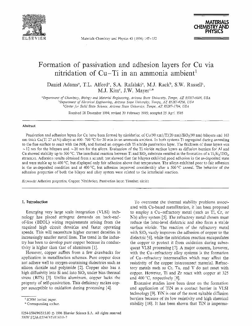
ELSEVIER Materials Chemistry and Physics 43 (1996) 145-152
Formation of passivation and adhesion layers for Cu via nitridation of Cu-Ti in an ammonia ambient’
Daniel Adamsa, T.L. Alford”, S.A. Rafalski”, M. J. Rackb, S.W. Russell”, M.J. Kim”, J.W. Mayerc,*
“Department of Chemistry, Biology and Material Engineering, Arizona State UMversity, Tetnpe, AZ 85287-6006, USA bDepartmerlt of Electrical Engineering, Arizona State University, Tenzpe, AZ 85287-6206, USA
‘Center for Solid State Science, Arizona State University, Tempe, AZ 85287-1704, USA
Received 28 December 1994; revised 20 February 1995; accepted 25 April 1995
Abstract
Passivation and adhesion layers for Cu have been formed by nitridation of Cu(90 nm)/Ti(20 nm)/Si0,(90 nm) bilayers and 163 nm thick Cu(Ti 27 at.%) alloys at 400-700 “C for 30 min in an ammonia ambient. In both systems Ti segregated during annealing to the free surface to react with the NH, and formed an oxygen-rich Ti nitride passivation layer. The thickness of these layers was N 12 nm for the bilayers and -20 nm for the alloys. E’valuation of the Ti nitride surface layers as diffusion barriers for Al and Cu showed stability up to 500 “C. The interfacial reaction between Ti and SiO, substrate resulted in the formation of a Ti,Si,/TiO,V structure. Adhesion results obtained from a scratch test showed that the bilayers exhibited good adhesion in the as-deposited state and were stable up to 400 “C, but displayed only fair adhesion above that temperature. The alloys exhibited poor to fair adhesion in the as-deposited condition and at 400 “C, but adhesion improved considerably after a 500 “C anneal. The behavior of the adhesion properties of both the bilayer and alloy system were related to the interfacial reaction.
Keywords: Adhesion properties; Copper; Nitridation; Passivation layer; Titanium nitride
1. Introduction
Emerging very large scale integration (VLSI) tech- nology has placed stringent demands on back-end- of-line (BEOL) wiring requirements arising from the required high circuit densities and faster operating speeds. This will necessitate higher current densities in increasingly smaller metal lines. The trend in the indus- try has been to develop pure copper because its conduc- tivity is higher than that of aluminum [ 11.
However, copper suffers from a few drawbacks for application in metallization schemes. Pure copper does not adhere well to oxygen-containing dielectrics such as silicon dioxide and polyimide [2]. Copper also has a high diffusivity into Si and into SiOl? under bias thermal stress (BTS) [3]. Unlike aluminum, copper lacks the property of self-passivation. This deficiency makes cop- per susceptible to oxidation during processing [4].
’ ICEM invited paper. * Corresponding author.
0254-0584/96/$15.00 0 1996 Elsevier Science S.A. All rights reserved SSD~~2_54~0~584f95‘)01610-7
To overcome the thermal stability problems associ- ated with Cu-based metallization, it has been proposed to employ a &-refractory metal (such as Ti, Cr, or Nb) alloy system [5]. The refractory metal chosen must reduce the inter-level dielectric and also form a stable surface nitride. The reaction of the refractory metal with SiOz vastly improves the adhesion of copper to the dielectric [6], while the nitridation reaction encapsulates the copper to protect it from oxidation during subse- quent VLSI processing [7]. A major concern, however, with the Cu-refractory alloy systems is the formation of Cu-refractory intermetallics which may affect the resistivity of the copper interconnect material. Refrac- tory metals such as Cr, Ta, and V do not react with copper. However, Ti and Zr react with copper at 325 and 400 “C, respectively [8].
Extensive studies have been done on the formation and application of TIN as a contact barrier in VLSI technology [9]. TIN is one of the most suitable diffusion barriers because of its low resistivity and high chemical stability [lo]. It has been shown that TIN is imperme-
146 D. Adam et al. /Materials Chemistry and Physics 43 (1996) 145-152
able to Si and Al [II], and it is an effective diffusion barrier in Cu/TiN/Si and Cu/TiN/Al structures up to 500 “C [ 121. Various methods have been employed to improve the adhesion of Cu to SiOZ: insertion of a metal adhesion promoter, such as Cr [ 131 or Ti [3], or addition of small amounts (lo-15 at.%) of various alloying elements [ 141. Russell et al. [6] have demon- strated good adhesion of Cu to SiO,-based dielectrics by alloying and subsequently annealing both Cu(Ti) and Cu(Cr) alloy films.
In the present investigation we have isochronally annealed Cu/Ti bilayers and Cu-Ti alloys in flowing NH3 to form TiN-encapsulated Cu layers. The two systems are contrasted with respect to the free surface reaction between Ti and NH, and the interfacial reaction between Ti and SiO, substrate. Also the stability of the TiN,( 0) resulting from the free surface reactions in both systems was evaluated for Cu and Al diffusion. We also investigated the adhesion of Cu/Ti bilayers and alloys on SiOZ using scratch testing. The adhesion properties of Cu to the SiO, substrate showed direct correlation with the interfacial reactions.
2. Experimental
A thin bilayer structure, Cu(90 nm)/Ti(20 nm), was prepared by sequentially depositing Ti and Cu by elec- tron-beam evaporation onto thermally grown silicon dioxide (SiOJ substrate. A 163 nm thick Cu(Ti 27 at.%) alloy was codeposited by electron-beam evapora- tion onto a 130 nm thermally grown SiO, substrate. The base and operating pressures of the deposition system were -lo-* and 10e7 Torr, respectively. The stoichiometry and thicknesses of the as-deposited sam- ples were determined by Rutherford backscattering spectrometry (RBS). Samples were annealed for 30 min at temperatures ranging from 400-700 “C in a Lindberg single-zone quartz tube furnace in a flowing electronic grade ammonia (NH,: 99.99 + %, with H,O < 33 and 0, + Ar < 10 molar ppm) ambient. A 50 nm Al film was deposited after nitridation, whereupon a second anneal was performed in flowing Ar-5%H, or N,- 5%H, forming gas. Al depositions were carried out by resistive evaporation in a bell-jar evaporator at a pres- sure of 10m6 Torr during deposition. To reduce the amount of oxygen during annealing, the chamber was evacuated to about 10 mTorr before each anneal, fol- lowed by a 2.5 min purge with NH, or the particular forming gas. This sequence was repeated twice with a final 20 min purge. To minimize the chances of oxida- tion, flow rates of about 8 1 min-’ were maintained during the anneals. Annealed samples were allowed to cool in the flowing gas before removal.
Free surface and interfacial reactions were analyzed by RBS and Auger electron spectroscopy (AES). The
microstructure and composition of the samples were also characterized by high resolution transmission elec- tron microscopy (HREM) and electron energy loss nanospectroscopy (EELS). RBS analysis was per- formed using a 1.7 MV Tandem accelerator using 2.0 and 3.7 MeV He*+ beams. The backscattering angle was 170” and the total accumulated charge lo-20 PC. The higher energy beam was used to detect the presence of nitrogen in the annealed samples, and to separate the overlapping copper and titanium signals. The samples were also tilted by 45 ’ to improve depth resolution. The N(cl,a)N nuclear reaction occurs near 3.7 MeV. All the samples were isochronally annealed for 30 min in a flowing NH, ambient. We utilized the computer-simula- tion program RUMP for simulation and interpretation of RBS spectra [15]. AES analyses of the bilayer sys- tems were performed by using a Perkin-Elmer PHI 600 scanning Auger system using a primary beam energy of 3 keV and a current of 0.2 PA. Depth profiles were acquired by sputtering with 3.5 keV Ar ions. The ion beam was rastered over a 2 mm2 area. The Auger instrument used to analyze the Cu-Ti alloy system was a Perkin-Elmer PHI stationary electron-beam thin-film analyzer which was controlled by a desktop microcom- puteF using a PC-137 interface. A 5 keV primary elec- tron beam of 3 JJA was used for excitation of the Auger spectra. The diameter of the beam was 250 pm. Depth profiles were acquired by sputtering with 2 keV Ar ions, directed at 30 ’ to the sample surface normal and rastered over a few millimeters. It should be noted that no attempt was made to separate the overlapping Ti (LMM) and N (KLL) transitions near 380 eV.
Cross sections of specimens for transmission electron microscopy (TEM) were prepared by mechanically thinning to about 100 llrn thickness and then dimpling 10 pm or less. Final thinning to electron transparency was done by Ar ion-beam milling. HREM experiments were performed in a Topcon-002B microscope at 200 kV, with a resolution limit of 0.18 nm. Nanoanalysis was done using a Philips EM400ST field emission gun microscope coupled to a Gatan parallel detection elec- tron energy loss spectrometer at 100 keV. A liquid-ni- trogen-cooled specimen holder was used for all analytical experiments to minimize specimen contami- nation and local specimen heating. For nano-diffraction and EELS experiments, the probe position was adjusted in diffraction mode by monitoring a shadow image in the Bragg disk of the transmitted beam. A computer system was utilized to control the focused probe posi- tion at the specimen and EELS spectrum acquisition for position-resolved spectroscopy.
Adhesion testing was performed by scratch testing at a fixed load applied in 10 g increments. The sample matrixes used for the adhesion measurements were: a bilayer structure of Cu( 180 nm) on Ti( 10 mn) and a 160 nm Cu(Ti 20 at.%) alloy on SiO,. Anneals were
D. Adams et al. /Matesink Chemistry and Physics 43 (1996) 145-152 147
‘2 I!
SO, z!
2 p Cu(Ti) z
x CA 9
600°C, 30 min, NH,
Sputter time (min)
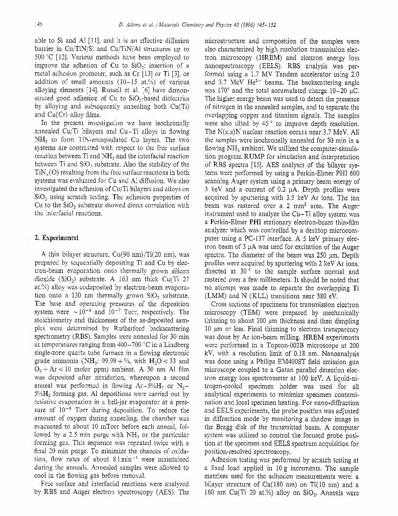
Fig. 1. Auger depth profiles of Cu(90 nm)/Ti(20 nm)/SiO, nitrided at 600 “C for 30 min in NH,.
performed under flowing ( - 1 1 min-‘) electronic grade forming gas (Ar-S%H,). All anneal times were 30 min. A complete description of the scratch tester and the failure criteria used for the scratch test are outlined in Ref. [6].
Substrate exposure was determined primarily by opti- cal microscopy at 40 x , Scanning electron microscopy and energy dispersive spectroscopy were used to verify exposure for selected samples.
3. Results
3.1. Free surface and interfacial reactions
3.1.1. Cu/Ti bilayer system In Fig. 1 AES depth profiles of the Cu( 90 nm) /Ti( 20
nm)/SiO, bilayer structure annealed at 600 “C are repre- sented. The depth profiles show that Ti segregates to the free surface. The segregated surface Ti reacts with the NH, ambient to form a Ti nitride surface layer, labeled as TIN,(O) on the schematic. Although the N-KLL and Ti-LMM signals near 380 eV overlap, the enhancement of the 380 eV Ti peak points to the presence of N in the surface layer. The profile based on this 380 eV peak is indicated by the label Ti + N for the 600 “C anneal as shown in Fig. 1. The decrease in the Ti signal to near background level in the subsurface layer suggests an almost pure copper layer. The oxygen profile shows, apart from the 0 peak from the SiO, substrate (near 18 rnin), an additional 0 peak near 12 min. The additional 0 peak originates from the dissociation of the SiOz by Ti at this temperature. As the oxide is dissociated, silicon reacts with Ti and forms a Ti silicide (labeled Ti,Si, on schematic) adjacent to the SiOz and the freed 0 reacts with the Ti to form a Ti oxide. In these analyses the Si window was set at 76-102 eV.
Energy (MeV) 1.5 2.0 2.5 3 ‘LO
I I I
-As-deposited - -5OO’C,
3.7 MeV 30 min
- -6OO”C, 30 min
I I I 300 400 500
Channel
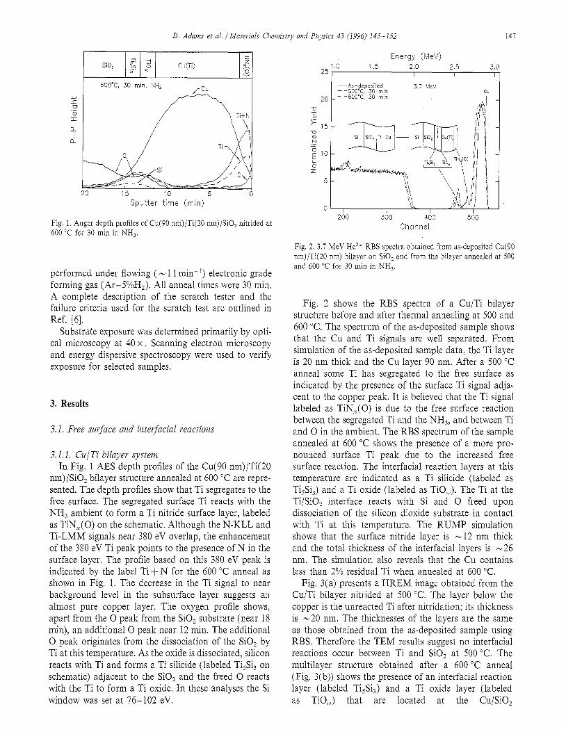
Fig. 2. 3.7 MeV He*+ RBS spectra obtained from as-deposited Cu(90 nm)/Ti(20 nm) bilayer on SiO, and from the bilayer annealed at 500 and 600 “C for 30 min in NH,.
Fig. 2 shows the RBS spectra of a Cu/Ti bilayer structure before and after thermal annealing at 500 and 600 “C. The spectrum of the as-deposited sample shows that the Cu and Ti signals are well separated. From simulation of the as-deposited sample data, the Ti layer is 20 nm thick and the Cu layer 90 nm. After a 500 “C anneal some Ti has segregated to the free surface as indicated by the presence of the surface Ti signal adja- cent to the copper peak. It is believed that the Ti signal labeled as TiN,(O) is due to the free surface reaction between the segregated Ti and the NH,, and between Ti and 0 in the ambient. The RBS spectrum of the sample annealed at 600 “C shows the presence of a more pro- nounced surface Ti peak due to the increased free surface reaction. The interfacial reaction layers at this temperature are indicated as a Ti silicide (labeled as Ti,Si,) and a Ti oxide (labeled as TiO,,,). The Ti at the Ti/SiO* interface reacts with Si and 0 freed upon dissociation of the silicon dioxide substrate in contact with Ti at this temperature. The RUMP simulation shows that the surface nitride layer is - 12 nm thick and the total thickness of the interfacial layers is -26 nm. The simulation also reveals that the Cu contains less than 2% residual Ti when annealed at 600 “C.
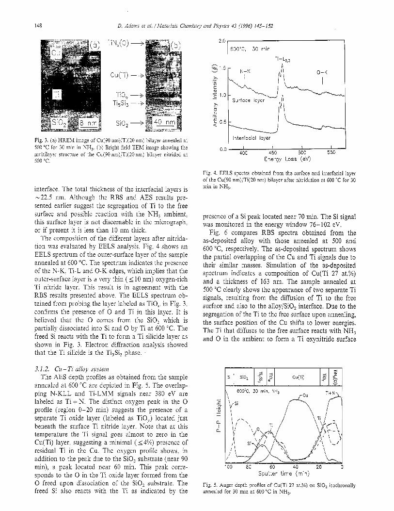
Fig. 3(a) presents a HREM image obtained from the Cu/Ti bilayer nitrided at 500 “C. The layer below the copper is the unreacted Ti after nitridation; its thickness is -20 nm. The thicknesses of the layers are the same as those obtained from the as-deposited sample using RBS. Therefore the TEM results suggest no interfacial reactions occur between Ti and SiOz at 500 “C. The multilayer structure obtained after a 600 “C anneal (Fig. 3(b)) shows the presence of an interfacial reaction layer (labeled Ti,Si,) and a Ti oxide layer (labeled as TiO,,) that are located at the Cu/SiO,
148 D. Adams ef al. /Materials Chemisrry and Physics 43 (1996) 145-152
EN,(O)
Cu(Ti)
Ti O,,, Ti,Si,
SiO,
2.0 600T, 30 min
Ti-L2,3
Fig. 3. (a) HREM image of Cut90 nm)/Ti(20 nm) bilayer annealed at 500 “C for 30 min in NH,. (b) Bright field TEM image showing the multilayer structure of the Cu(90 nm)/Ti(ZO nm) biIayer nitrided at 600 “C.
interface. The total thickness of the interfacial layers is -22.5 nm. Although the RBS and AES results pre- sented earlier suggest the segregation of Ti to the free surface and possible reaction with the NH3 ambient, this surface layer is not discernable in the micrograph, or if present it is less than 10 nm thick.
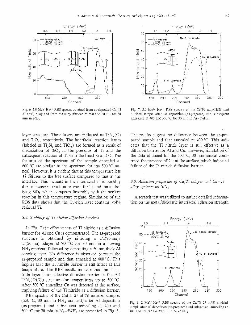
The composition of the different layers after nitrida- tion was evaluated by EELS analysis. Fig. 4 shows an EELS spectrum of the outer-surface layer of the sample annealed at 600 “C. The spectrum indicates the presence of the N-K, Ti-L and O-K edges, which implies that the outer-surface layer is a very thin ( I 10 nm) oxygen-rich Ti nitride layer. This result is in agreement with the RBS results presented above. The EELS spectrum ob- tained from probing the layer labeled as TiO,, in Fig. 3, confirms the presence of 0 and Ti in this layer. It is believed that the 0 comes from the SiO, which is partially dissociated into Si and 0 by Ti at 600 “C. The freed Si reacts with the Ti to form a Ti silicide layer as shown in Fig. 3. Electron diffraction analysis showed that the Ti silicide is the Ti,Si, phase.
3.1.2. Cu - Ti alloy system The AES depth profiles as obtained from the sample
annealed at 600 “C are depicted in Fig. 5. The overlap- ping N-KLL and Ti-LMM signals near 380 eV are labeled as Ti t N. The distinct oxygen peak in the 0 profile (region O-20 min) suggests the presence of a separate Ti oxide layer (labeled as TiO,) located just beneath the surface Ti nitride layer. Note that at this temperature the Ti signal goes almost to zero in the Cu(Ti) layer, suggesting a minimal ( 14%) presence of residual Ti in the Cu. The oxygen profile shows, in addition to the peak due to the SiOZ substrate (near 90 mm), a peak located near 60 min. This peak corre- sponds to the 0 in the Ti oxide layer formed from the 0 freed upon dissociation of the SiOZ substrate. The freed Si also reacts with the Ti as indicated by the
Interfacial layer
0.0 I 1 I I 400 450 500 550
Energy Loss (eV)
Fig. 4. EELS spectra obtained from the surface and interfacial layer of the Cu(90 nm)/Ti(20 nm) bilayer after nitridation at GO0 ‘C for 30 min in NH,.
presence of a Si peak located near 70 min, The Si signal was monitored in the energy window 76-102 eV.
Fig. 6 compares RBS spectra obtained from the as-deposited alloy with those annealed at 500 and 600 “C, respectively. The as-deposited spectrum shows the partial overlapping of the Cu and Ti signals due to their similar masses. Simulation of the as-deposited spectrum indicates a composition of Cu(Ti 27 at.%) and a thickness of 163 nm, The sample annealed at 500 “C clearly shows the appearance of two separate Ti signals, resulting from the diffusion of Ti to the free surface and also to the alloy/SiO, interface. Due to the segregation of the Ti to the free surface upon annealing, the surface position of the Cu shifts to lower energies. The Ti that diffuses to the free surface reacts with NH, and 0 in the ambient to form a Ti oxynitride surface
,:! zi 3
Si SiO, $2 P CufTi) $ g v
600°C, 30 min, NH3
2 0 .-
?
a I
a
Sputter time (min)
Fig. 5. Auger depth profiles of Cu(Ti 27 at.%) on SiO, isochronally annealed for 30 min at 600 “C in NH,.
D. Adams et al. /Materials Chemistry nrd Physics 43 (1996) 145-152 149
Energy (MeV) 0.6 0.8 1.0 1.2 1.4 1.6
I I I I I
80
t
-As-deposited - -5OO’C, 30 min - -6OOT, 30 min
0 \\ ,, 1
160 I I I
150 200 250
Channel
Fig. 6. 2.0 MeV He2* RBS spectra obtained from as-deposited Cu(Ti 27 at.%) alloy and from the alloy nitrided at 500 and 600 “C for 30 min in NH,.
layer structure. These layers are indicated as TIN,(O) and TiO,, respectively. The interfacial reaction layers (labeled as Ti,Si, and TiO,,) are formed as a result of dissociation of SiOZ in the presence of Ti and the subsequent reaction of Ti with the freed Si and 0. The features of the spectrum of the sample annealed at 600 “C are similar to the spectrum for the 500 ‘C an- neal. However, it is evident that at this temperature less Ti diffuses to the free surface compared to that at the interface. This increase in the interfacial Ti is possibly due to increased reaction between the Ti and the under- lying Si02 which competes favorably with the surface reaction in this temperature regime. Simulation of the RBS data shows that the &-rich layer contains ~4% residual Ti.
3.2. Stability of Ti nitride dlj%sion hurriers
In Fig. 7 the effectiveness of Ti nitride as a diffusion barrier for Al and Cu is demonstrated. The as-prepared structure is obtained by nitriding a Cu(90 nm)/ Ti(20 nm) bilayer at 700 “C for 30 min in a flowing NH, ambient, followed by depositing a 50 nm thick Al capping layer. No difference is observed between the as-prepared sample and that annealed at 400 “C. This implies that the Ti nitride barrier is still intact at this temperature. The RBS results indicate that the Ti ni- tride layer is an effective diffusion barrier in the Al/ TiN,.(O)/Cu structure for temperatures up to 500 “C. After 500 “C annealing Cu was detected at the surface, implying failure of the Ti nitride as a diffusion barrier.
RBS spectra of the Cu(Ti 27 at.%) nitrided samples (550 “C, 30 min in NH, ambient) after Al deposition (as-prepared) and subsequent annealing at 400 and 500 “C for 30 min in N,-5%H2 are presented in Fig. 8.
Energy (MeV)
1.1 12 1.3 1.4 1.5 1.6 70, I , I I I I I
60
7J 40 2 .-
0 30 E k5
z 20
10
Channel
Fig. 7. 2.0 MeV He2+ RBS spectra of the Cu(90 nm)/Ti(20 nm) nitrided sample after Al deposition (as-prepared) and subsequent annealing at 400 and 500 “C for 30 min in Ar-S%H,.
The results suggest no difference between the as-pre- pared sample and that annealed at, 400 “C. This indi- cates that the Ti nitride layer is still effective as a diffusion barrier for Al and Cu. However, simulation of the data obtained for the 500 “C, 30 min anneal confi- rmed the presence of Cu at the surface, which indicated failure of the Ti nitride diffusion barrier.
3.3. Adhesion properties of CulTi bilayer and Cu-Ti alloy systems on SOS
A scratch test was utilized to gather detailed informa- tion on the metal/dielectric interfacial adhesion strength
Energy (MeV) 1 .o 1.2 1.4 1.6
70 I I 1
60
; 50
jr qJ 40 E
.% 30 E b
z 20
10
Channel
Fig. 8. 2 MeV He2+ RBS spectra of the Cu(Ti 27 at.%) nitrided sample after Al deposition (as-prepared) and subsequent annealing at 400 and 500 “C for 30 min in N,-5%H2.
150 D. Adams et al. /Materials Chemistry and Physics 43 (1996) 145-152
80
57 0 Cu/Ti Bilayer
E 6o
A Cu(Ti) Alloy
*NA
2
2 40 -y/Y o-o
-i :q 20 -
;
0 I I I 0 200 400 600
Temperature (“C)
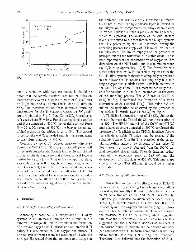
Fig. 9. Scratch test results for Cu/Ti bilayers and Cu-Ti alloys on SiO,.
and its evolution with heat treatment. It should be noted that the sample matrixes used for the adhesion measurements were: a bilayer structure of Cu( 180 nm) on Ti( 10 nm) and a 160 nm Cu(Ti 20 at.%) alloy on SiOz. The measured critical force W versus annealing temperature for the Ti bilayer structure on SiOz sub- strate is plotted in Fig. 9. Pure Cu on Si02 is used as a reference where W = 10 g. For the as-deposited samples and those annealed at 400 “C the resulting critical force W = 50 g. However, at 500 “C, the bilayer system ex- hibited a drop in the critical force to 40 g. The critical forces for the 600 “C annealed samples were equivalent to the values obtained at 500 “C.
Contrary to the Cu/Ti bilayer structures discussed above, the Cu(Ti 20 at.%) alloys did not adhere as well in the as-deposited state. Scratch test results are plotted in Fig. 9. The data indicate that a lower critical force is needed for failure (W = 30 g) in the as-deposited state, although this is still a significant improvement over pure Cu on SiO, (W =,lO g). It is apparent that addi- tions of Ti greatly enhance the adhesion of Cu to dielectrics. The critical force increases slightly in value after annealing to 400 “C. At 500 “C and above, the critical force increases significantly to values greater than or equal to 55 g.
4. Discussion
4.1. Free surface and interfacial reactions
Annealing of both the Cu/Ti bilayer and Cu-Ti alloy systems in an ammonia ambient for 30 min in the temperature range 400-600 “C results in the formation of a surface oxygen-rich Ti nitride and an interfacial Ti oxide/Ti silicide structure. The oxygen-rich surface Ti nitride layer is formed from the reaction of Ti with the nitrogen dissociated from the ammonia and oxygen in
the ambient. The results clearly show that a thinner ( N 12 nm at 600 “C) single surface layer is formed in the bilayer system compared to the alloys where a dual Ti oxide/Ti nitride surface layer ( -20 nm at 600 “C) structure is present. The absence of the dual surface layer is attributed to the fact that in the bilayer systems the Ti is protected by the Cu. Therefore, during the annealing process the supply of Ti is much less than in the alloy case. The limited supply and the presence of nitrogen retards the formation of a stable oxide. It has been reported that the concentration of oxygen in Ti is dependent on the N/Ti ratio, and is a minimum when the N/Ti ratio approaches I [16]. The formation of a stable subsurface oxide in the surface region (as in the Cu-Ti alloy system) is therefore completely suppressed in the bilayer Cu-Ti systems, resulting only in a thin single oxygen-rich Ti nitride layer. This is in contrast to the Cu-Ti alloy where Ti is almost immediately avail- able for reaction with the 0 in the ambient at the onset of the annealing process. The AES results Cu(Ti 27 at.%) in Fig. 5 confirmed the formation of a stable subsurface oxide (labeled TiO,,). This oxide did not inhibit the nitridation as observed by the presence of the surface Ti nitride layer (TiN,Y(0)) in Fig. 5.
A Ti silicide is formed on top of the SiOz due to the reaction between the Ti and the Si upon dissociation of the SiO*. The HREM analysis of the Cu(90 nm)/Ti (20 nm) bilayer structure annealed at 600 “C! confirmed the presence of a Ti silicide at the Ti/SiOl interface. Above the silicide a stable Ti oxide may be formed if the solubility limit of 0 in the Ti is exceeded at the partic- ular annealing temperature. A study of the Auger Ti line shapes (not shown) obtained from the 600 “C an- neal presented characteristic Ti oxide features: reduc- tion of the secondary peak at 385 eV and the development of a shoulder at 410 eV. This line shape closely resembles TiO although it could be a higher oxide state.
4.2. Evaluation of cl~j%sion bat&r.s
In this section we discuss the effectiveness of TiN,(O) barriers formed by annealing Cu/Ti bilayers and alloys formed by isochronally (30 min) nitriding the structures in an NH3 ambient at 700 and 550 “C, respectively. RBS analysis indicated no difference between the Cu/ TiN,(O)/Al sample annealed at 400 “C for 30 min in Ar-5%Hz and the as-prepared sample (Fig. 7). How- ever, the results obtained for the 500 “C anneal showed the presence of Cu at the surface, which suggested failure of the TiN diffusion barrier. The results further suggested that the TiN film dissociates as an effect of the barrier failure. Aluminum can be nitrided and cop- per can react with Ti to form compounds when they make contact with the TiN during heat treatment. Therefore, it is believed that the formation of Al,Ti,
D. Adams et al. /Materials Chemistry and Physics 43 (1996) 145-152 151
Cu,Ti and AlN compounds of the barrier were primar- ily responsible for the dissociation of the TiN barriers. Evaluation of the integrity of the nitrided Cu-Ti alloy system as diffusion barriers for Cu and Al showed a failure mechanism similar to that of the bilayer system. The TIN diffusion barrier in this case was also only stable up to 500 “C. Therefore, the results indicate that in both systems the TIN,(O) was stable as a diffusion barrier for Cu and Al up to 500 “C. However, it is important to point out that the bilayer structure had to be nitrided at 700 “C to have equivalent barrier effec- tiveness as the alloy nitride at 550 “C.
J.3. Adhesion properties of CulTi bilayer and Cu-Ti dloy systems on SO,
As the temperature is increased for the Cu-Ti alloys, the amount of Ti which segregates to the dielectric interface increases steadily. This correlates well with the adhesion results where the transition from fair adhesion to good adhesion occurs at around 500 “C. These re- sults can be summarized in the following statement: adhesion is enhanced in the Cu(Ti 20 at.%) alloy sys- tems by an interfacial reaction that is occurring via reduction of SiOz by Ti, and the analysis indicates only a small amount of reaction is needed for improved interfacial strength.
The observed results for the Cu/Ti bilayers cannot solely be explained by chemical effects. The shift to lower critical forces above 400 “C in the bilayer system is difficult to explain since it is expected that the degree of chemical interaction between Ti and the dielectric will increase with higher annealing temperature. One explanation is that at the free surface a reaction occurs which draws some of the Ti to the free surface leaving behind Kirkendall voids at the Cu/dielectric interface due to the rapid rate at which these species are diffus- ing. These voids would cause the interfacial strength to weaken by decreasing the interfacial area. Preliminary transmission electron microscopy studies suggest that voids may have formed near the dielectric interface in the Cu/Ti bilayer at 500 “C.
5. Conclusions
Nitridation of Cu/Ti bilayer and Cu-Ti alloy systems at temperatures 400-700 “C in NH3 for 30 min resulted in the segregation of Ti to both the free surface and alloy/SiO, interface. The Ti that segregated to the free surface reacted with the NH, ambient to form a Ti oxynitride passivation layer. Application of these sur- face layers as diffusion barriers for Cu and Al showed stability up to 500 “C. At temperatures as low as 500 “C, Ti at the Cu/SiO, interface reduces the SiO*. The freed Si and 0 react with the Ti to form a
Ti,Si,/Ti oxide structure between the Cu and the re- maining SiOz substrate. The evolution of the final struc- ture is therefore governed by a competition between the free surface nitridation/oxidation and the interfacial reaction. The residual Ti in the encapsulated Cu layer was always <4%.
Bilayers exhibit good adhesion in the as-deposited state and are stable to 400 “C but display only fair adhesion above that temperature, whereas alloys exhibit poor to fair adhesion in the as-deposited condition and at 400 “C, but adhesion improves considerably at and above the 500 “C anneal. The improvement of adhesion in the alloy structures is attributed to chemical reac- tions between Ti and the SiO*. The degradation in adhesion in the bilayer structures is attributed to void- ing at the interface as Ti diffuses away from the inter- face to the free surface.
It is clearly evident that low temperature ( 1600 “C) nitridation of Cu-Ti alloys yields thicker Ti nitride passivation/diffusion layers than the bilayers and the alloys also displayed improved adhesion properties on SiOz in this temperature regime. Therefore, Cu-based alloys have a future in semiconductor metallization schemes because they have been proven to have electri- cal and mechanical characteristics comparable to bilay- ers after heat treatment.
Acknowledgements
The authors would like to thank Harland Tompkins (Motorola, Mesa, AZ) for performing some of the AES analyses. They also acknowledge the financial support provided by the National Science Foundation (L. Hess, DMR-9307662 and L. Salmon, ECS-9410399).
References
[l] J.M.E. Harper, K.L. Holloway and T.Y. Kwok, US Patent No. 5 130 274, 1992.
[2] C. Apblett, D. Muira, M. Sullivan and P.J. Ficalora, J. Appl. Phys., 71 (1992) 4925.
[3] Y. Shacham-Diamand, A. Dedhia, D. Hoffstetter and W.G. Oldham, J. Electrochem. Sot., 140 (1993) 2421.
[4] J. Li, G. Vizkelethy, P. Revesz, J.W. Mayer and K.N. Tu, J. Appl. Phys., 69 (1991) 1020.
[5] J. Li, J.W. Mayer, Y. Shacham-Diamand and E.G. Colgan, Appl. Phys. Lett., 60 (1992) 2983.
[ 61 SW. Russell, S.A. Rafalski, R.L. Spreitzer, J. Li, M. Moinpour, F. Moghadam and T.L. Alford, Thin Solid Fibns, submitted for publication.
[7] J. Li, J.W. Mayer and E.G. Colgan, J. Appl. Phys., 70 (1991) 2820.
[8] J. Li, J.W. Strane, S.W. Russell, S.Q. Hong, J.W. Mayer, T.K. Marais, CC. Theron and R. Pretorius, J. iippl. Phys., 72 (1992) 2810.
[9] C.Y. Ting, S.S. Iyer, CM. Osburn, G.J. Hu and A.M. Scheiw- gart, Proc. First Im. Symp. VLSI Science and Technology, The Electrochemical Society, New York, 1982, p. 224.

152 D. Adam et al. /Matesials Chemistry and Physics 43 (1996) 145-l-U
[lo] M.A. Nicolet and M. Bartur, J. Vat. Ski. Techml., 19 (1981) 786.
[ 111 M. Kottke, R. Gregory, F. Pintchovski, E. Travis and P.J. Tobin, J. Vat. Sci. Technol. B, 9 (1) (1991) 74.
1121 S.Q. Wang, I. Raaijmakers, B.J. Burrow, S. Suthar, S. Redkar and K.B. Kim, J. Appl. Phys., 68(1990) 5176.
[13] A.R. Wolter, J. Appl. Phys., 36 (1965) 2377. [14] K. Hoshino, H. Yagi and H. Tsuchikawa, Pvoc. 7fk Iut. IEEE
VLSI Mtiltileuel Interconnection Co& 1991, p, 357. [ 151 L.R. Doolittle, Nucl. Iustwn~. Methods B, 9 (1985) 344. [ 161 M.M. Farahani, S. Garg and B.T. Moore, J. Ebxttvchcn~. Sot.,
141 (1994) 479.