Embed Size (px)
Citation preview
August 2012 physicsworld.com
FOCUS ON VACUUM TECHNOLOGY
Challenges, applications and solutions

Monitor and control your vacuum systems with the most reliable technology from Oerlikon Leybold Vacuum. Precision vacuum measurement is crucial for the success of vacuum processes and research. Vacuum transmitters, control-ler, as well as passive sensors and their operating instruments help to maintain the parameters of your manufacturing processes in the pressure range from 10-12 to 1000 mbar, some even under radiation and bakeable conditions. For professional leak detection, the helium leak detector PHOENIXL is designed for industrial applications - robust, fast and extremely accurate. The modular cart version with an built-in scroll pump SC30 D offers even more flexibility. Get the details at www.oerlikon.com/leyboldvacuum
High Vacuum Monitoring and Control
Smart technology you can rely on
©B
ICO
M_1
1618
.02
3.07
.201
2
Oerlikon Leybold Vacuum GmbHBonner Strasse 498D-50968 KölnT +49 (0)221 347-0F +49 (0)221 347-1250E-mail : [email protected]://www.oerlikon.com/leyboldvacuum
Augus t 2012 1
physicswor ld.com
Physics World Focus on: Vacuum technology
Contents
Who says CERN’s discovery of the Higgs boson has no Physics World
it is also providing a springboard for the energy sector. That
Matin Durrani, Editor, Physics World
On the coverRotor blades in a turbomolecular pump 27 (Agilent Technologies)
Focus on: Vacuum technology
Thin-film solar cells offer major market opportunities 3
Vacuum technology underpins nanotechnology research at Sheffield University 19
Editor Matin DurraniAssociate Editor Dens MilneNews Editor Michael BanksContributing Editor Susan CurtisProduction Editor Louise Unwin
Managing Editor Susan CurtisMarketing and Circulation Gemma BaileyAdvertisement Sales Chris ThomasAdvertisement Production Mark TrimnellDiagram Artist Alison ToveyArt Director Andrew Giaquinto
Copyright © 2012 by IOP Publishing Ltd and individual contributors. All rights reserved
Printed in the UK by Warners (Midlands) plc, The Maltings, West Street, Bourne, Lincolnshire PE10 9PH
Physics WorldTemple Circus, Temple Way, Bristol BS1 6HG, UKTel: +44 (0)117 929 7481E-mail: [email protected]: physicsworld.com
News 3Edwards raises $100m on NASDAQ Barriers to thin-film solar cells Roadmap for plasmas unveiled Angstrom launches novel CVD kit Silicene revealed Yoctogram mass sensor Synchrotrons in focus
FeaturesFrom beam pipes to solar panels 9Marina Giampietro describes how vacuum technology used at CERN’s Large Hadron Collider is boosting the solar revolution
Growing graphene for real 13Vacuum techniques lie at the heart of attempts to grow large amounts of high-quality graphene for real-world applications, explains Belle Dumé
Welcome to nanotech central 19A novel research facility at Sheffield University that could lead to novel electronic devices deploys vital vacuum techniques, reports Matthew Chalmers
Agilent expands vacuum offering 23Giampaolo Levi, head of Agilent’s new Vacuum Products division, tells Susan Curtis how the company is benefiting from its acquisition of Varian in 2010
How low can you go? 27Richard Stevenson describes the technology required to go from normal atmospheric pressure down to extreme vacuum levels
Events Diary 30Key meetings, conferences and exhibitions in the vacuum-technology calendar
EMPA
Uni
vers
ity
of S
heff
ield

Exceptional high performance
nXDS - for heightened performance and reliability with lower cost of ownership
nXDS - the great new shape of high performance dry vacuum pumping
Vacuum science... product solution.
© Edwards Limited 2012. All Rights Reserved
Discover more at www.edwardsvacuum.com/nXDS
Totally outclassing the competition
Augus t 2012 3
physicswor ld.com NewsPhysics World Focus on: Vacuum technology
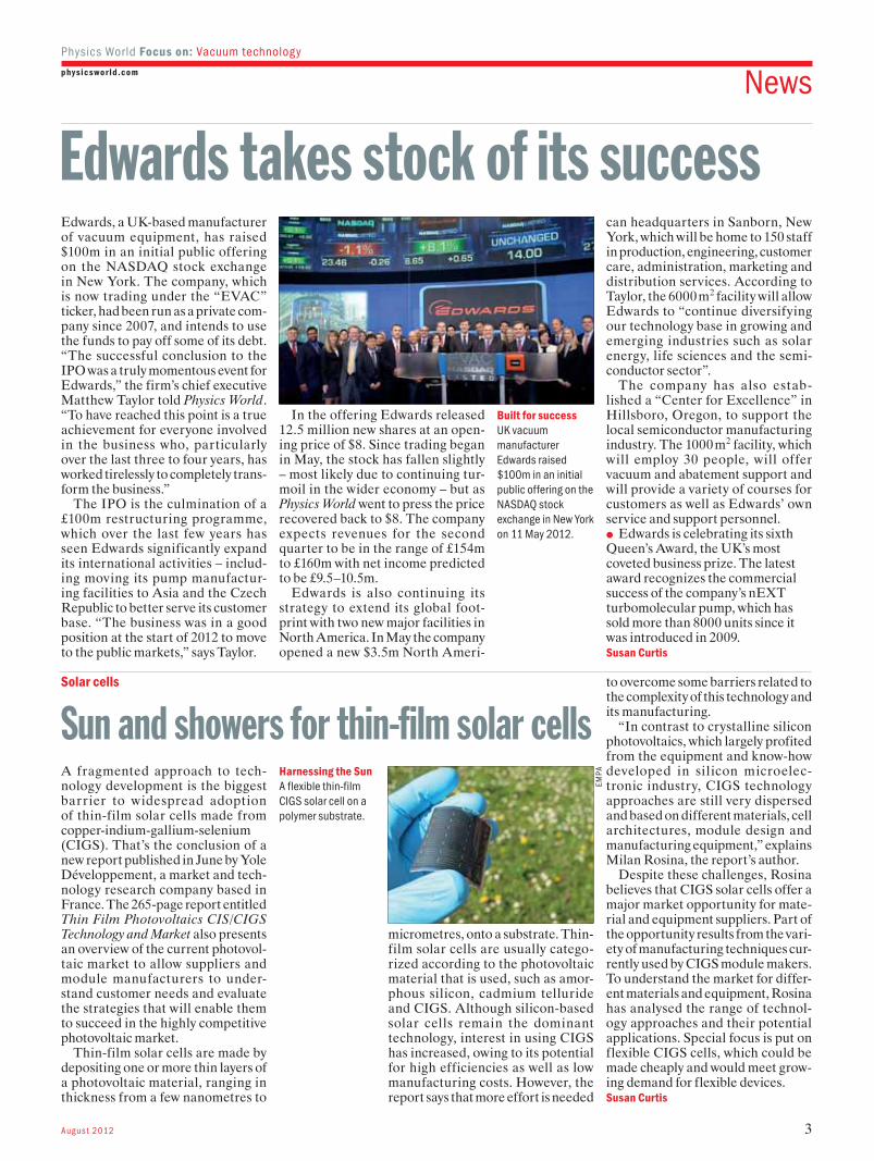
Edwards, a UK-based manufacturer of vacuum equipment, has raised $100m in an initial public offering on the NASDAQ stock exchange in New York. The company, which is now trading under the “EVAC” ticker, had been run as a private com-pany since 2007, and intends to use the funds to pay off some of its debt. “The successful conclusion to the IPO was a truly momentous event for Edwards,” the firm’s chief executive Matthew Taylor told Physics World. “To have reached this point is a true achievement for everyone involved in the business who, particularly over the last three to four years, has worked tirelessly to completely trans-form the business.”
The IPO is the culmination of a £100m restructuring programme, which over the last few years has seen Edwards significantly expand its international activities – includ-ing moving its pump manufactur-ing facilities to Asia and the Czech Republic to better serve its customer base. “The business was in a good position at the start of 2012 to move to the public markets,” says Taylor.
In the offering Edwards released 12.5 million new shares at an open-ing price of $8. Since trading began in May, the stock has fallen slightly – most likely due to continuing tur-moil in the wider economy – but as Physics World went to press the price recovered back to $8. The company expects revenues for the second quarter to be in the range of £154m to £160m with net income predicted to be £9.5–10.5m.
Edwards is also continuing its strategy to extend its global foot-print with two new major facilities in North America. In May the company opened a new $3.5m North Ameri-
Edwards takes stock of its successcan headquarters in Sanborn, New York, which will be home to 150 staff in production, engineering, customer care, administration, marketing and distribution services. According to Taylor, the 6000 m2 facility will allow Edwards to “continue diversifying our technology base in growing and emerging industries such as solar energy, life sciences and the semi-conductor sector”.
The company has also estab-lished a “Center for Excellence” in Hillsboro, Oregon, to support the local semiconductor manufacturing industry. The 1000 m2 facility, which will employ 30 people, will offer vacuum and abatement support and will provide a variety of courses for customers as well as Edwards’ own service and support personnel.
Edwards is celebrating its sixth Queen’s Award, the UK’s most coveted business prize. The latest award recognizes the commercial success of the company’s nEXT turbomolecular pump, which has sold more than 8000 units since it was introduced in 2009.Susan Curtis
Built for success UK vacuum manufacturer Edwards raised $100m in an initial public offering on the NASDAQ stock exchange in New York on 11 May 2012.
Harnessing the Sun A flexible thin-film CIGS solar cell on a polymer substrate.
A fragmented approach to tech-nology development is the biggest barrier to widespread adoption of thin-film solar cells made from copper-indium-gallium-selenium (CIGS). That’s the conclusion of a new report published in June by Yole Développement, a market and tech-nology research company based in France. The 265-page report entitled Thin Film Photovoltaics CIS/CIGS Technology and Market also presents an overview of the current photovol-taic market to allow suppliers and module manufacturers to under-stand customer needs and evaluate the strategies that will enable them to succeed in the highly competitive photovoltaic market.
Thin-film solar cells are made by depositing one or more thin layers of a photovoltaic material, ranging in thickness from a few nanometres to
micrometres, onto a substrate. Thin-film solar cells are usually catego-rized according to the photovoltaic material that is used, such as amor-phous silicon, cadmium telluride and CIGS. Although silicon-based solar cells remain the dominant technology, interest in using CIGS has increased, owing to its potential for high efficiencies as well as low manufacturing costs. However, the report says that more effort is needed
to overcome some barriers related to the complexity of this technology and its manufacturing.
“In contrast to crystalline silicon photovoltaics, which largely profited from the equipment and know-how developed in silicon microelec-tronic industry, CIGS technology approaches are still very dispersed and based on different materials, cell architectures, module design and manufacturing equipment,” explains Milan Rosina, the report’s author.
Despite these challenges, Rosina believes that CIGS solar cells offer a major market opportunity for mate-rial and equipment suppliers. Part of the opportunity results from the vari-ety of manufacturing techniques cur-rently used by CIGS module makers. To understand the market for differ-ent materials and equipment, Rosina has analysed the range of technol-ogy approaches and their potential applications. Special focus is put on flexible CIGS cells, which could be made cheaply and would meet grow-ing demand for flexible devices.Susan Curtis
Sun and showers for thin-film solar cells Solar cells
EMPA
INTRODUCING THE MODEL 22C
Two multipurpose input channels support most cryogenic temperature sensors. Thermocouple inputs are optional.
Two-channel Cryogenic Temperature ControllerTwo-channel Cryogenic Temperature Controller
www.cryocon.com
physicswor ld.com NewsPhysics World Focus on: Vacuum technology
Augus t 2012 5
Technology updateEdwards introduces new rangeUK vacuum manufacturer Edwards has launched a new range of dry-scroll vacuum pumps for scientific applications. The company claims that the new nXDS is the best performing pump in its class, offering exceptional pumping capability and state-of-the-art design features. According to Edwards, it is a simple “fit and forget” pump that provides excellent performance for many years. The oil-free pump avoids the need for lubricants, which reduces the need for regular maintenance, resulting in less downtime and a low cost of ownership. It also has a lower environmental impact than oil-sealed pumps, including a standby mode to reduce power consumption, while the advanced scroll design and tip-seal technology make it extremely reliable.
New leak detector from PfeifferGerman firm Pfeiffer Vacuum has introduced the first vacuum leak detector that uses a quartz-window sensor to detect helium instead of the usual mass spectrometer. This means that the MiniTest 300 operates reliably at pressures up to 200 mbar, while other leak detectors work at only about 20 mbar. As the MiniTest is a helium partial-pressure measuring device that requires no internal pumping system, the maintenance costs are also lower than for traditional leak detectors. The device is small and light enough to be used for on-site service calls, and also offers wireless remote control to allow even large facilities and systems to be tested by a single engineer. It can be used for a range of industrial applications, such as coating and vacuum systems, as well as for vacuum furnaces.
UHV Design showcases productsA new brochure from UHV Design details how its vacuum manipulation products can be used in synchrotron applications. The guide showcases the capabilities of devices ranging from linear actuators to complete multi-axis sample manipulators. The document outlines each type of manipulator commonly used in synchrotron applications, and provides examples of how they are used in storage rings, beamlines and end stations. UHV Design says that its products can meet the demands of the synchrotron community for precision, durability and ultrahigh vacuum performance, and that it also offers in-house expertise to customize its products to meet specific requirements.
A group of 16 leading plasma researchers from Japan, the Neth-erlands, the US, France, Germany, Australia and the UK, has released a roadmap defining the current trends and future challenges for plasma sci-ence and technology. Split into 16 sections that are each on a specialist sub-field of plasma physics, The 2012 Plasma Roadmap, which has been published in Journal of Physics D: Applied Physics (45 253001), details the current state of the art as well as the challenges that lie ahead for each of the fields.
Plasma processing under vacuum conditions is tackled by several experts. Seiji Samukawa of Tohoku University, Japan, surveys plasma etching for future nanoscale devices, while Shahid Rauf of US-based com-pany Applied Materials covers very large-area plasma processing for applications such as semiconductor chips, flat-panel displays and solar panels. Other key areas featured in the roadmap include plasma lighting, “nanodusty” plasmas for fabricating nanoparticle-based materials, and modelling and diagnostics.
With such a diverse set of appli-cations – extending to plasmas for medicine, catalysis and the environ-
Plasma experts map out the road ahead
Built for growth A new chemical vapour deposition system from Angstrom Engineering will allow researchers to fabricate carbon nanotubes and graphene.
Angstrom Engineering has launched a low-pressure chemical vapour deposition system that has been optimized for graphene and carbon nanotube research. As interest grows in the use of graphene for a range of thin-film electronic devices, Ang-strom has released a system that com-bines precise process control along with the flexibility to experiment with different growth conditions.
The new system has been specifi-cally designed to provide the high temperatures and rapid cooling needed to fabricate such novel mate-rials. Angstrom has designed a water-cooled furnace that can be heated to 1100 °C within 10 minutes, which sig-nificantly reduces the process time. It can also be cooled to below 800 °C within two minutes, which is critical
for controlled graphene growth. A fully automated control system
allows researchers to specify pro-cess recipes with up to 50 separate steps, and data logs are captured to the results from each recipe to be analysed. Safety is also ensured through a complete interlock system that protects users from the extreme temperatures, process gases and high voltages that occur in this type of equipment.
The system offers stable pressure control from 100 mTorr to 500 Torr and it can accommodate up to 12 mass f low controllers. Chamber sizes range in diameter from 50 to 200 mm, allowing processing of sin-gle small samples up to batches of 150 mm wafers.Susan Curtis
New deposition system targets graphene researchMaterials science
Plasma physics
ment – it has proved difficult to pro-duce a single view on research trends. “There’s no single person who can give an overview of all of these dif-ferent directions. Instead we asked a larger group of experts to write short articles on their particular area,” guest editor Uwe Czarnetzki of the Ruhr-University Bochum in Germany told Physics World during a video interview.
What emerges is a detailed snap-shot of current activities in plasma research, which the authors say include “novel technologies, fresh ideas and concepts, and new appli-cations”. If the roadmap succeeds in its goal to provide greater clarity about plasma research to political and funding bodies, the authors say that they will update the roadmap to reflect continuing innovation in a rapidly evolving field. “Novel tech-nologies, fresh ideas and concepts, and new applications discussed by our authors demonstrate that the road to the future is wide and far reaching,” the authors write. “We hope that this special plasma roadmap will provide guidance for colleagues, funding agencies and government institutions.”Susan Curtis
We hope that this special plasma roadmap will provide guidance for colleagues, funding agencies and government institutions
detecting the future
[email protected] | www.dectris.com
Specific solutions
– In-vacuum detectors – Specific module geometries– Special energy calibrations
SINGLE-PHOTON- COUNTING X-RAY DETECTORS
In-vacuum PILATUS 1M detector for X-ray detection down to 1.75 keV, realized in collaboration with the Physikalisch-Technische Bundesanstalt, Berlin.
Specific solutions are based on our successful PILATUS and MYTHEN detector series.
physicswor ld.com NewsPhysics World Focus on: Vacuum technology
Augus t 2012 7
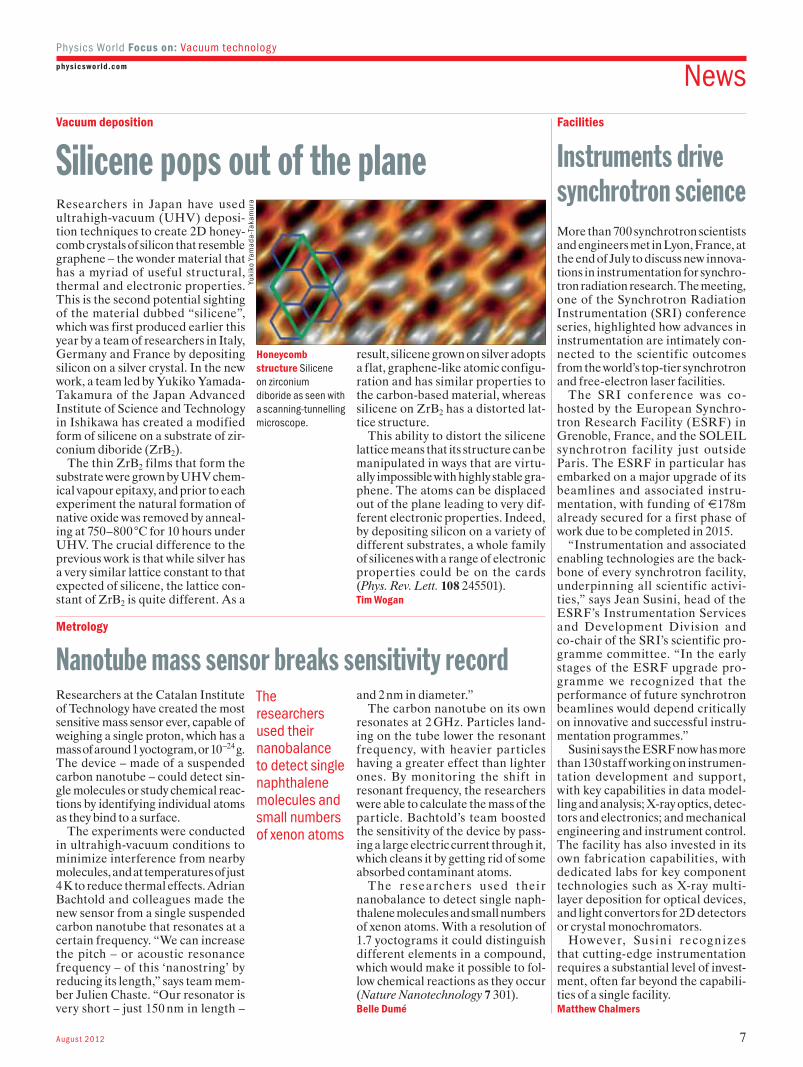
Researchers in Japan have used ultrahigh-vacuum (UHV) deposi-tion techniques to create 2D honey-comb crystals of silicon that resemble graphene – the wonder material that has a myriad of useful structural, thermal and electronic properties. This is the second potential sighting of the material dubbed “silicene”, which was first produced earlier this year by a team of researchers in Italy, Germany and France by depositing silicon on a silver crystal. In the new work, a team led by Yukiko Yamada-Takamura of the Japan Advanced Institute of Science and Technology in Ishikawa has created a modified form of silicene on a substrate of zir-conium diboride (ZrB2).
The thin ZrB2 films that form the substrate were grown by UHV chem-ical vapour epitaxy, and prior to each experiment the natural formation of native oxide was removed by anneal-ing at 750–800 °C for 10 hours under UHV. The crucial difference to the previous work is that while silver has a very similar lattice constant to that expected of silicene, the lattice con-stant of ZrB2 is quite different. As a
result, silicene grown on silver adopts a flat, graphene-like atomic configu-ration and has similar properties to the carbon-based material, whereas silicene on ZrB2 has a distorted lat-tice structure.
This ability to distort the silicene lattice means that its structure can be manipulated in ways that are virtu-ally impossible with highly stable gra-phene. The atoms can be displaced out of the plane leading to very dif-ferent electronic properties. Indeed, by depositing silicon on a variety of different substrates, a whole family of silicenes with a range of electronic properties could be on the cards (Phys. Rev. Lett. 108 245501).Tim Wogan
Honeycomb structure Silicene on zirconium diboride as seen with a scanning-tunnelling microscope.
Researchers at the Catalan Institute of Technology have created the most sensitive mass sensor ever, capable of weighing a single proton, which has a mass of around 1 yoctogram, or 10–24 g. The device – made of a suspended carbon nanotube – could detect sin-gle molecules or study chemical reac-tions by identifying individual atoms as they bind to a surface.
The experiments were conducted in ultrahigh-vacuum conditions to minimize interference from nearby molecules, and at temperatures of just 4 K to reduce thermal effects. Adrian Bachtold and colleagues made the new sensor from a single suspended carbon nanotube that resonates at a certain frequency. “We can increase the pitch – or acoustic resonance frequency – of this ‘nanostring’ by reducing its length,” says team mem-ber Julien Chaste. “Our resonator is very short – just 150 nm in length –
More than 700 synchrotron scientists and engineers met in Lyon, France, at the end of July to discuss new innova-tions in instrumentation for synchro-tron radiation research. The meeting, one of the Synchrotron Radiation Instrumentation (SRI) conference series, highlighted how advances in instrumentation are intimately con-nected to the scientific outcomes from the world’s top-tier synchrotron and free-electron laser facilities.
The SRI conference was co-hosted by the European Synchro-tron Research Facility (ESRF) in Grenoble, France, and the SOLEIL synchrotron facility just outside Paris. The ESRF in particular has embarked on a major upgrade of its beamlines and associated instru-mentation, with funding of 178m already secured for a first phase of work due to be completed in 2015.
“Instrumentation and associated enabling technologies are the back-bone of every synchrotron facility, underpinning all scientific activi-ties,” says Jean Susini, head of the ESRF’s Instrumentation Services and Development Division and co-chair of the SRI’s scientific pro-gramme committee. “In the early stages of the ESRF upgrade pro-gramme we recognized that the performance of future synchrotron beamlines would depend critically on innovative and successful instru-mentation programmes.”
Susini says the ESRF now has more than 130 staff working on instrumen-tation development and support, with key capabilities in data model-ling and analysis; X-ray optics, detec-tors and electronics; and mechanical engineering and instrument control. The facility has also invested in its own fabrication capabilities, with dedicated labs for key component technologies such as X-ray multi-layer deposition for optical devices, and light convertors for 2D detectors or crystal monochromators.
However, Susin i recognizes that cutting-edge instrumentation requires a substantial level of invest-ment, often far beyond the capabili-ties of a single facility. Matthew Chalmers
and 2 nm in diameter.”The carbon nanotube on its own
resonates at 2 GHz. Particles land-ing on the tube lower the resonant frequency, with heavier particles having a greater effect than lighter ones. By monitoring the shift in resonant frequency, the researchers were able to calculate the mass of the particle. Bachtold’s team boosted the sensitivity of the device by pass-ing a large electric current through it, which cleans it by getting rid of some absorbed contaminant atoms.
The researchers used thei r nanobalance to detect single naph-thalene molecules and small numbers of xenon atoms. With a resolution of 1.7 yoctograms it could distinguish different elements in a compound, which would make it possible to fol-low chemical reactions as they occur (Nature Nanotechnology 7 301).Belle Dumé
Nanotube mass sensor breaks sensitivity recordMetrology
Silicene pops out of the planeVacuum deposition
Yuki
ko Y
amad
a-Ta
kam
ura
Instruments drive synchrotron science
Facilities
The researchers used their nanobalance to detect single naphthalene molecules and small numbers of xenon atoms
Augus t 2012 9
physicswor ld.com SolarPhysics World Focus on: Vacuum technology
From beam pipes to solar panels
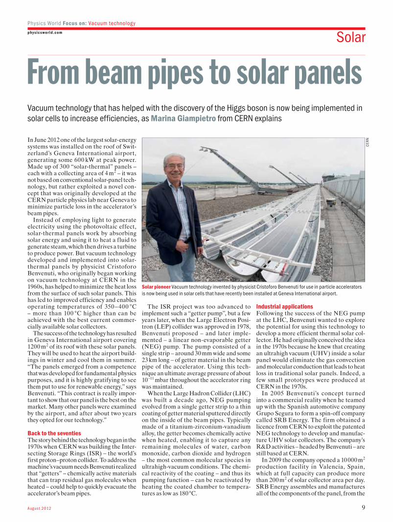
In June 2012 one of the largest solar-energy systems was installed on the roof of Swit-zerland’s Geneva International airport, generating some 600 kW at peak power. Made up of 300 “solar-thermal” panels – each with a collecting area of 4 m2 – it was not based on conventional solar-panel tech-nology, but rather exploited a novel con-cept that was originally developed at the CERN particle physics lab near Geneva to minimize particle loss in the accelerator’s beam pipes.
Instead of employing light to generate electricity using the photovoltaic effect, solar-thermal panels work by absorbing solar energy and using it to heat a fluid to generate steam, which then drives a turbine to produce power. But vacuum technology developed and implemented into solar-thermal panels by physicist Cristoforo Benvenuti, who originally began working on vacuum technology at CERN in the 1960s, has helped to minimize the heat loss from the surface of such solar panels. This has led to improved efficiency and enables operating temperatures of 350–400 °C – more than 100 °C higher than can be achieved with the best current commer-cially available solar collectors.
The success of the technology has resulted in Geneva International airport covering 1200 m2 of its roof with these solar panels. They will be used to heat the airport build-ings in winter and cool them in summer. “The panels emerged from a competence that was developed for fundamental physics purposes, and it is highly gratifying to see them put to use for renewable energy,” says Benvenuti. “This contract is really impor-tant to show that our panel is the best on the market. Many other panels were examined by the airport, and after about two years they opted for our technology.”
Back to the seventiesThe story behind the technology began in the 1970s when CERN was building the Inter-secting Storage Rings (ISR) – the world’s first proton–proton collider. To address the machine’s vacuum needs Benvenuti realized that “getters” – chemically active materials that can trap residual gas molecules when heated – could help to quickly evacuate the accelerator’s beam pipes.
The ISR project was too advanced to implement such a “getter pump”, but a few years later, when the Large Electron Posi-tron (LEP) collider was approved in 1978, Benvenuti proposed – and later imple-mented – a linear non-evaporable getter (NEG) pump. The pump consisted of a single strip – around 30 mm wide and some 23 km long – of getter material in the beam pipe of the accelerator. Using this tech-nique an ultimate average pressure of about 10–11 mbar throughout the accelerator ring was maintained.
When the Large Hadron Collider (LHC) was built a decade ago, NEG pumping evolved from a single getter strip to a thin coating of getter material sputtered directly on the inside of the beam pipes. Typically made of a titanium-zirconium-vanadium alloy, the getter becomes chemically active when heated, enabling it to capture any remaining molecules of water, carbon monoxide, carbon dioxide and hydrogen – the most common molecular species in ultrahigh-vacuum conditions. The chemi-cal reactivity of the coating – and thus its pumping function – can be reactivated by heating the coated chamber to tempera-tures as low as 180 °C.
Industrial applicationsFollowing the success of the NEG pump at the LHC, Benvenuti wanted to explore the potential for using this technology to develop a more efficient thermal solar col-lector. He had originally conceived the idea in the 1970s because he knew that creating an ultrahigh vacuum (UHV) inside a solar panel would eliminate the gas convection and molecular conduction that leads to heat loss in traditional solar panels. Indeed, a few small prototypes were produced at CERN in the 1970s.
In 2005 Benvenuti’s concept turned into a commercial reality when he teamed up with the Spanish automotive company Grupo Segura to form a spin-off company called SRB Energy. The firm obtained a licence from CERN to exploit the patented NEG technology to develop and manufac-ture UHV solar collectors. The company’s R&D activities – headed by Benvenuti – are still based at CERN.
In 2009 the company opened a 10 000 m2 production facility in Valencia, Spain, which at full capacity can produce more than 200 m2 of solar collector area per day. SRB Energy assembles and manufactures all of the components of the panel, from the
Vacuum technology that has helped with the discovery of the Higgs boson is now being implemented in solar cells to increase efficiencies, as Marina Giampietro from CERN explains
Solar pioneer Vacuum technology invented by physicist Cristoforo Benvenuti for use in particle accelerators is now being used in solar cells that have recently been installed at Geneva International airport.
CER
N
physicswor ld.comSolarPhysics World Focus on: Vacuum technology
collector structure up to the vacuum pro-cess, and also designs and produces support structures and mirrors that can allow light collection for maximum efficiency.
The solar thermal collectors now being produced by SRB Energy can absorb more than 70% of solar energy with very small heat emission. Tests show that the UHV thermal solar panel can even produce 80 °C with a thick layer of snow on top of the collector, while other collectors produce almost nothing under the same conditions.
The vacuum level inside the panel varies between 10–6 and 10–9 mbar during the daily solar cycle, but SRB Energy claims that the vacuum is remarkably stable over time, with the same pumping function being main-tained for 25 years or more. This means that the panels are suitable for a range of commercial applications, including domes-tic and industrial heating, air conditioning and energy generation.
The collectors are available in a range of configurations for different applications. The flat collector on its own is most suitable for domestic use, where it can be installed on a roof and used to power a hot-water heating system. As the UHV panel converts diffuse light into heat with high efficiency, it is particularly suitable for countries where
the sun does not shine every day.“High-temperature solar-cell operation
can normally only be achieved by concen-trating the solar radiation using parabolic mirrors, but these designs can be expensive and are unable to collect diffuse solar energy in cloudy conditions,” says Benvenuti. How-ever, these new collectors can achieve tem-peratures of up to 300 °C without the use of focusing mirrors. “Our panels are also specially designed to collect both direct and diffuse sunlight, which makes them very pro-ductive in terms of energy. Diffuse sunlight corresponds to more than half of central Europe’s solar energy, but can’t be collected by systems that use focusing mirrors.”
Industrial heating processes typically require higher temperatures, and in this case the flat collector can be combined with a cylindrical concentration system to reli-ably achieve working temperatures of up to
200 °C. SRB has already supplied panels for various projects, including heating a paint oven to 175 °C for use in the automotive industry, and heating tanks of bitumen to 190 °C for an asphalt-manufacturing facility.
Even higher temperatures are needed for large heating systems and power gen-eration, and for these applications SRB has devised a concentration system based on Fresnel mirrors. However, Benvenuti believes that the unique properties of the UHV collector would enable more solar energy to be harvested over the course of the year, while lower operating tempera-tures would also reduce the overall bill of materials for the plant.
Benvenuti hopes that the order from Geneva International airport will now pave the way for commercial success. “Other pro-jects in Switzerland and France are close to being signed off, and the completion of this project will certainly help to generate some great publicity for this technology.” For CERN, meanwhile, SRB Energy is a shin-ing example of how technologies developed for fundamental physics can drive innova-tion in the commercial sector.
Marina Giampietro is a communication officer at CERN
The solar thermal collectors can absorb more than 70% of solar energy with very small heat emission
© Copyright 2012. COMSOL, COMSOL Multiphysics and LiveLink are either registered trademarks or trademarks of COMSOL AB. AutoCAD and Inventor are registered trademarks of Autodesk, Inc., in the USA and other countries. LiveLink for AutoCAD and LiveLink for Inventor
®
Verify and optimize your designs with COMSOL Multiphysics.
COMSOL Multiphysics
FLUIDCFD Module Pipe Flow ModuleMicrofluidics ModuleSubsurface Flow Module
CHEMICALChemical Reaction Engineering Module Batteries & Fuel Cells ModuleElectrodeposition Module Corrosion Module
MECHANICALHeat Transfer ModuleStructural Mechanics Module Nonlinear Structural Materials ModuleGeomechanics Module Acoustics Module
ELECTRICALAC/DC ModuleRF ModuleMEMS ModulePlasma Module
MULTIPURPOSEOptimization ModuleMaterial LibraryParticle Tracing Module
INTERFACINGCAD Import ModuleFile Import for CATIA® V5LiveLink™ for SolidWorks®
LiveLink™ for SpaceClaim®
LiveLink™ for Pro/ENGINEER®
LiveLink™ for Creo™ ParametricLiveLink™ for Inventor®
LiveLink™ for AutoCAD®
LiveLink™ for MATLAB®
Product Suite
Multiphysics tools let you build simulations that accurately replicate the important characteristics of your designs. The key is the ability to include all physical effects that exist in the real world. Order your free Introduction to Multiphysics CD at www.comsol.com/intro
®®
CVD: Chemical Vapor Deposition in low-pressure reactors is an
deposition on wafers as a function of the reactor operating conditions.
COMSOLCONFERENCEEUROPE 20 1 2 OCTOBER 10 - 12
Vacuum feedthrough
DIAMOND SAVia dei Patrizi 5, CH-6616 LosoneTel.+41 91 785 45 45, Fax +41 91 785 45 00
www.diamond-fo.com
Based on UHV CF flangeConnectorized or pigtailedWide choice of connector typesMAS universal flanges for highmodularity
High optical performanceSuitable for every fiber typeCompatible with PM fibers
Aeronautics and marineLaboratory and measurementapplicationsVacuum chambers and pressurevesselsOil and gas industry
Compatible connectors
FC AVIM Mini-AVIM DIN DMI
J A N I S
Contact us today:[email protected] +1 978 657-8750www.janis.com/ProbeStations.aspxwww.facebook.com /JanisResearch
Applications include nano science, materials and spintronics3.2 K - 675 K; high vacuum or UHVUp to 8 probes, DC to 67 GHz, plus fiber opticsZoom optics with camera and monitor Cooling options: liquid helium, liquid nitrogen or cryogen freeHorizontal, vertical or vector magnetic field options are available
Cryogenic Wafer Probe Stations
Augus t 2012 13
physicswor ld.com GraphenePhysics World Focus on: Vacuum technology
Growing graphene for real
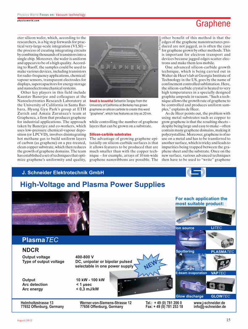
Graphene – a sheet of carbon atoms arranged in a honeycomb-like lattice just one atom thick – is the “wonder material” that could revolutionize electronics and possibly even replace silicon as the indus-try’s material of choice. Its unique prop-erties arise partly from the fact that the electrons in graphene behave as if they have no rest mass, which means that they streak through the material at about 0.3% of the speed of light – an invaluable prop-erty in the quest for ultrafast transistors. Indeed, owing to the fact that they move at such high speeds, the electrons in graphene are called “Dirac fermions” because they are governed by the Dirac equation – the quantum-mechanical description of elec-trons moving relativistically.
Graphene also has an abnormally high strength for a one-atom-thick material. Indeed, if a 100 μm-thick sheet of cling film had the same strength as pristine gra-phene, you would require a force of more than 20 000 N to puncture it with a pencil – roughly that exerted by a 2 tonne car. Moreover, graphene shows great promise for photonics applications because almost every photon absorbed by the material gen-erates an electron-hole pair that could, in principle, be converted into electric cur-rent. And thanks to its Dirac electrons, gra-phene can also absorb light of any colour.
However, one big hurdle will have to be overcome if efficient real-world devices are to see the light of day – namely, that researchers will need to find a way of syn-thesizing high-quality graphene in a con-trolled way. Single layers of graphene can be isolated using the “Scotch-tape” technique, which simply involves lifting off flakes of the material from a piece of graphite (the form of carbon found in pencil lead) using sticky tape. Although this technique produces
monolayer samples of pure graphene ideal for fundamental studies – it was widely used by Andre Geim and Konstantin Novoselov from the University of Manchester in their Nobel-prize-winning work – it can in no way be scaled up to industrial levels.
There are currently two main ways to produce large-area, high-quality graphene suitable for the electronics industry, both of which require vacuum processes. The first involves creating a layer of the material on a copper film, while the second requires the graphene layer to be grown on structured silicon-carbide surfaces. Although the two methods have been known for decades, interest in them has intensified as research-ers have discovered how important gra-phene could be for the electronics industry.
Each technique has its own advantages
and disadvantages. Growing graphene on copper, for example, is relatively straight-forward and it allows the material to be produced over larger surface areas than is possible with silicon carbide. Unfor-tunately, graphene grown on copper is polycrystalline and contains grain bounda-ries that can degrade the electronic and mechanical properties of graphene. On the other hand, growing graphene with silicon carbide is more expensive because it is less cheap to use as a substrate.
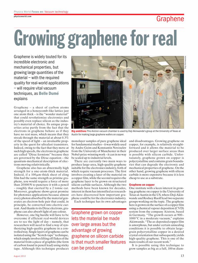
Graphene on copperOne institute with a keen interest in grow-ing graphene on copper is the University of Texas at Austin in the US, where Deji Akin-wande and Rodney Ruoff lead two separate groups working on the topic. The graphene here is grown on the surface of a copper film using a chemical vapour deposition (CVD) system from the company Aixtron, based in Germany. “The growth occurs at 900–1000 °C in a moderate vacuum,” explains Akinwande. “The as-deposited copper film is amorphous, but under certain annealing conditions it is possible to obtain large-grain polycrystalline copper in a desired crystal orientation that subsequently yields high-quality graphene. This is one of the main results of our recent work.”
It is possible using this technique to grow samples as big as a full, 100 m diam-
Graphene is widely touted for its incredible electronic and mechanical properties, but growing large quantities of the material – with the required quality for real-world applications – will require vital vacuum techniques, as Belle Dumé explains
Big ambitions This Aixtron vacuum chamber is used by Deji Akinwande’s group at the University of Texas at Austin for making large graphene wafers on copper.
Graphene grown on copper lets the material be made over large areas but the advantage of growing graphene on silicon carbide is that much smaller features can be produced
Dej
i Aki
nwan
de
AIXTRON SE · Kaiserstr. 98 · 52134 Herzogenrath · Germany · E-mail : [email protected] · www.aixtron.com
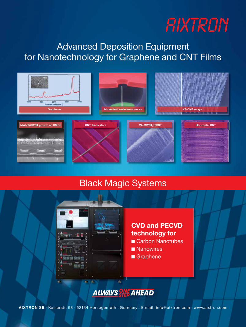
Advanced Deposition Equipment for Nanotechnology for Graphene and CNT Films
Black Magic Systems
MWNT/SWNT growth on CMOS
VA-CNF arraysMicro fi eld emission sourcesGraphene
CNT Transistors VA-MWNT/SWNT Horizontal CNT
CVD and PECVD technology for
Carbon NanotubesNanowiresGraphene
Augus t 2012 15
physicswor ld.com GraphenePhysics World Focus on: Vacuum technology
eter silicon wafer, which, according to the researchers, is a big step forwards for prac-tical very-large-scale integration (VLSI) – the process of creating integrating circuits by combining thousands of transistors into a single chip. Moreover, the wafer is uniform and appears to be of a high quality. Accord-ing to Ruoff, the samples could be used to make various devices, including transistors for radio-frequency applications, chemical/vapour sensors, transparent electrodes for displays, supercapacitors for energy storage and nanoelectromechanical systems.
Other key players in this field include Kaustav Banerjee and colleagues at the Nanoelectronics Research Laboratory at the University of California in Santa Bar-bara, Hyung Gyu Park’s group at ETH Zurich and Amaia Zurutuza’s team at Graphenea, a firm that produces graphene for industrial applications. The approach taken by Banerjee and co-workers, which uses low-pressure chemical-vapour depo-sition (or LPCVD), involves disintegrating hot methane gas to build uniform layers of carbon (as graphene) on a pre-treated, clean copper substrate, which then reduces the growth of graphene domains. The team has established a set of techniques that opti-mize graphene’s uniformity and quality,
while controlling the number of graphene layers that can be grown on a substrate.
Silicon-carbide substratesThe advantage of growing graphene epi-taxially on silicon-carbide surfaces is that it allows features to be produced that are much smaller than with the copper tech-nique – for example, arrays of 10 nm-wide graphene nanoribbons are possible. The
other benefit of this method is that the edges of the graphene nanostructures pro-duced are not jagged, as is often the case for graphene grown by other methods. This is important for electron transport and devices because jagged edges scatter elec-trons and make them less mobile.
One advanced silicon-carbide growth technique, which is being carried out in Walter de Heer’s lab at Georgia Institute of Technology in the US, goes by the name of confinement controlled sublimation. Here, the silicon-carbide crystal is heated to very high temperatures in a specially designed graphite ampoule in vacuum. “Such a tech-nique allows the growth rate of graphene to be controlled and produces uniform sam-ples,” explains de Heer.
As de Heer points out, the problem with using metal substrates such as copper to grow graphene is that the resulting sheets – despite being large and easy to make – often contain many graphene domains, making it polycrystalline. Moreover, graphene is of no use on a metal and has to be transferred to another surface, which is tricky and leads to impurities being trapped between the gra-phene sheet and the substrate. Once on the new surface, various advanced techniques then have to be used to “write” graphene
Small is beautiful Sefaattin Tongay from the University of California at Berkeley has grown graphene on silicon carbide to create this word “graphene”, which has features as tiny as 20 nm.
Sef
Ton
ngga
y
Helmholtzstrasse 13 Werner-von-Siemens-Strasse 12 Tel.: + 49 (0) 781 206 0 www.j-schneider.de
77652 Offenburg, Germany 77656 Offenburg, Germany Fax: + 49 (0) 781 253 18 [email protected]
J. Schneider Elektrotechnik GmbH
High-Voltage and Plasma Power Supplies
GLOWTEC
PLASMATEC
Glow discharge
NDCR
Sputtering
For each application the
most suitable product:
PLASMATEC
Ion source
LITEC
VAPTEC
E-beam evaporation
Output voltage 400-800 V
Type of output voltage DC, unipolar or bipolar pulsed
selectable in one power supply
Output 10 kW - 100 kW
Arc detection < 1 μsec
Arc energy < 0,3 mJ/kW
E
W
N
PlasmaTEC
16 Augus t 2012
physicswor ld.comGraphenePhysics World Focus on: Vacuum technology
Flexible drive concepts for HV and UHV environments: PI miCos and PI offer engineered vacuum solutions for single- and multi-axis precision positioning tasks.
Enthusiastic about technology – enthusiastic for you.
10-11 hPaE N G I N E E R E D V A C U U M S O L U T I O N S
W W W. P I M I C O S . C O M
Physik Instrumente (PI) GmbH & Co. KGAuf der Römerstr. 1 · 76228 KarlsruheTel. +49 (721) 4846-0 · Fax +49 (721) [email protected] · www.pi.ws
PI miCos GmbHFreiburger Str. 30 · 79427 Eschbach Tel. +49 (7634) 5057-0 · Fax +49 (7634) [email protected] · www.pimicos.com
nanopatterns, which leaves a lot of residue on the graphene surface. “In contrast, sili-con carbide is a high-quality single crystal, which is an important semiconductor in its own right, so graphene grown on this mate-rial can be directly used in electronics appli-cations,” says de Heer.
Technically, the graphene samples can be grown as large as the silicon-carbide wafer (3 inches), but smaller rectangles measur-ing 4 5 mm are preferred. “Bigger does not always mean better – it is all about quality,” says de Heer. “For electronics, well formed nanostructures on silicon carbide are much more interesting and important than very large, poorly formed sheets transferred from metals.”
Sefaattin Tongay of the University of California at Berkeley agrees. His group is working on implanting graphene on silicon-carbide substrates using various ions employing focused beam lithography and loading the samples into a vacuum oven to finalize the graphene growth process. Irradiating silicon carbide with ions creates open silicon and carbon bonds, explains Tongay, and during the annealing step the carbon rises to the surface and forms gra-phene. Without the ion-irradiation step, graphene growth would initiate at a higher
temperature. “Our technique is good for writing small features without too many complications,” he says. “And the whole process is as easy as implanting desired regions with ions, which is a routine tech-nique in the semiconductor industry any-way, and then just annealing the material in a vacuum. We have currently made some further developments and can now grow graphene even faster.”
Graphene grown on silicon carbide can be used to make electronics devices for basic scientific research. Narrow epitaxial graphene nanoribbons, the properties of which might be tuned from conducting to insulating according to some recent research, might ultimately be used as wir-ing for nanographene electronics as well as for making semiconducting graphene or graphene-derived semiconductors.
Copper and plastic electronicsAkinwande agrees that significant pro-gress has been made on growing graphene on single-crystal silicon-carbide substrates, which would allow the graphene to be used directly on such substrates without having to be transferred. However, he thinks it would be far too expensive to transfer graphene from such costly substrates to, say, polymer
films for plastic electronics, which is why – in his view – copper wins out. “Copper film can be large in size and so allows for very-large-area graphene growth for use in applica-tions like plastic electronics as transparent conductive films and RF electronics,” says Akinwande. Ruoff also claims that various groups, including his own, are improving the quality of the graphene grown on cop-per films and foils by obtaining material that has a larger grain size, which in turn shows higher carrier mobilities.
Materials scientist Manish Chhowalla from Rutgers University, meanwhile, thinks that CVD-grown graphene on copper is a promising method for producing continu-ous layers of high-quality material over large areas. “Wrinkles and grain bounda-ries are sparse in graphene grown on cop-per and therefore excellent optoelectronic properties can be obtained,” he says. But Chhowalla adds that the main challenge for this method will be to develop a “reli-able and scalable method” to remove the graphene from the copper and transfer it to other substrates. “If this and other problems can be overcome then graphene grown on copper could even replace indium tin oxide as the ubiquitous transparent conductor,” he claims.

Delivering Expert Solutions for Vacuum, Surface & Nanoscience
Scanwel Ltd, Llandderfel, Bala, Gwynedd LL23 7HW, UK. Tel: +44 (0)1678 530281. Fax: +44 (0)1678 530320
Photoelectron Spectroscopy under Near Ambient Pressures (NAP)
www.scanwel.co.uk
Making vacuum easy – from off the shelf hardware to complete custom systems
Scanwel three chamber xhv outgassing test system, with <10–11 mbar base pressure for Joe Herbert (ASTeC Vacuum Science Group Daresbury Laboratory).
• “Superclean” chambers separated by “sealed” Variable Orifice Disc
• xhv pumping based on turbo pumps in series and all metal gate valves
• 250 oC quick fit bakeout system
• Fast “heated” Entry lock for transfer to low maintenancesample outgassing stage for TPD studies
• Multiple RGA heads and “extractor gauges”
• Simple manual control system with power failure safe condition
Competitively priced hardware is available from stock. For a full listing, including details of this amazing offer visit our easy to use on-line shop
OFFER of the month
Key features• Wide Angle Pre-Lens with 44° Acceptance Angle• Near Ambient Working Pressures up to 25 mbar• Large Kinetic and Pass Energy Range• High Energy and Angular Resolution• Compatible with our unique in-situ high pressure cell• XPS and UPS excitation sources for NAP conditions• Complete systems available
When analysing properties of devices that function in ambient conditions, high pressures or liquid environments, the application of the results has always been controversial due to the usual vacuum environment in XPS and UPS. For years this pressure gap has been an insurmountable barrier. The SPECS Phoibos 150 NAP is a new product designed to bridge that gap, enabling ESCA measurements at pressures up to 25 mbar by the use of multiple differential pumping stages.
AVB-CF70Viton Sealed Valve
Usually £238 Less 20%Offer Price £190.40
are exclusively represented by Scanwel in the UK and Ireland

Competitive pricing and short lead times for standard and custom electrical feedthroughs.
www.lewvac.co.ukLewVac, Unit F2, Ote Hall Farm, Janes Lane, Burgess Hill, East Sussex, RH15 0SR, UKTel : +44 (0) 1444 233372 - email : [email protected] - Fax : +44 (0)1444 233392
D i f f r a c t i o n and Pos i t i o n i ng Equ i pmen t
Sommerstrasse 4
D-83253 Rimsting, Germany
www.xhuber.com
The World of High Precis ion
Vacuum Posit ioning
FV/HV/UHV
An t imagne t i c
Rad i a t i o n r e s i s t an t
S t anda rd o r cus t omer - spec i f i c s o l u t i o ns
Vacuum e xpe r i ence f o r more t han 20 y ea r s
Augus t 2012 19
physicswor ld.com FacilitiesPhysics World Focus on: Vacuum technology
Welcome to nanotech central
The semiconductor industry represents perhaps the most advanced nanotechnol-ogy there is, underpinning all aspects of modern telecommunications and consumer electronics. Silicon is the industry’s work-horse, but III-V semiconductors – materi-als in groups three and five of the Periodic Table – offer a higher carrier mobility and favourable optoelectronic properties. III-Vs drive the Internet, mobile phones and optical data storage, but also underpin applications such as high-efficiency solar cells and solid-state lighting, terahertz imaging for healthcare, and transistors that will further the miniaturization trend.
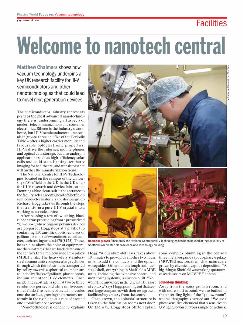
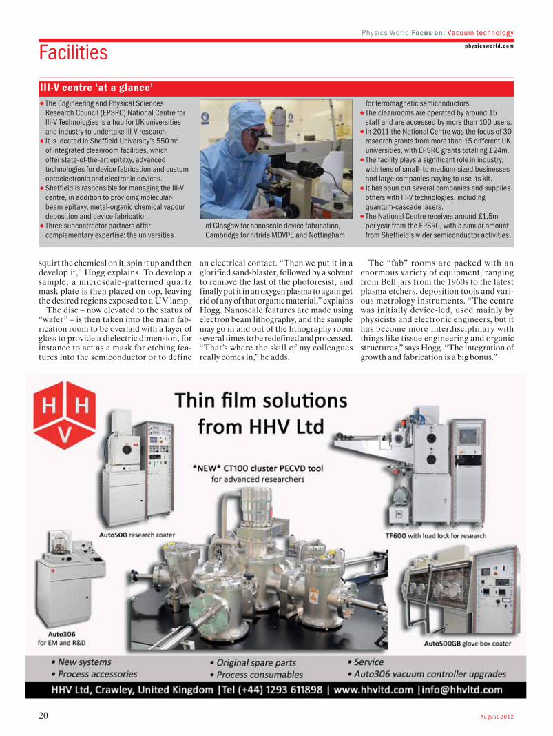
The National Centre for III-V Technolo-gies, located on the campus of the Univer-sity of Sheffield in the UK, is the UK’s hub for III-V research and device fabrication. Donning a blue clean-suit at the entrance to the facility’s cleanrooms, head of Sheffield’s semiconductor materials and devices group Richard Hogg takes us through the steps that transform a pure III-V crystal into a working nanoscale device.
After passing a row of twitching, black rubber arms protruding from a pressurized “glove box”, where organic polymer devices are prepared, Hogg stops at a plastic tub containing 350 μm-thick polished discs of gallium arsenide a few centimetres in diam-eter, each costing around £70 ($125). These, he explains above the noise of equipment, are the substrates that are loaded into one of the centre’s three molecular-beam-epitaxy (MBE) units. The heavy-duty stainless-steel vacuum units comprise a large cylinder through which the substrate is transported by trolley towards a spherical chamber sur-rounded by flasks of gallium, phosphorous, indium and other III-V elements. Once inside, the substrate is spun at two or three revolutions per second while millisecond-timed flasks fire beams of metal molecules onto the surface, growing the structure uni-formly in the x-y plane at a rate of around one atomic layer per second.
“Nanotechnology is done in z,” explains
Hogg. “A quantum-dot laser takes about 10 minutes to grow, plus another two hours or so to add the contacts and the optical waveguide.” Other than its tough stainless-steel shell, everything in Sheffield’s MBE units, including the extensive control and monitoring systems, is custom built. “You won’t find anywhere in the UK with this sort of epitaxy,” says Hogg, pointing out that sev-eral large companies with their own growth facilities buy epitaxy from the centre.
Once grown, the epitaxial structure is taken to the fabrication rooms next door. On the way, Hogg stops off to explain
some complex plumbing in the centre’s three metal-organic vapour-phase-epitaxy (MOVPE) reactors, in which structures are grown by chemical vapour deposition. “A big thing at Sheffield was making quantum-cascade lasers on MOVPE,” he says.
Joined-up thinkingAway from the noisy growth room, and with more staff around, we are bathed in the unsettling light of the “yellow room”, where lithography is carried out. “We use a photosensitive chemical that’s sensitive to UV light, so you put your sample on a chuck,
Matthew Chalmers shows how vacuum technology underpins a key UK research facility for III-V semiconductors and other nanotechnologies that could lead to novel next-generation devices
Room for growth Since 2007 the National Centre for III-V Technologies has been housed at the University of Sheffield’s dedicated Nanoscience and Technology building.
All i
mag
es: U
nive
rsit
y of
She
ffie
ld
20 Augus t 2012
physicswor ld.comFacilitiesPhysics World Focus on: Vacuum technology
squirt the chemical on it, spin it up and then develop it,” Hogg explains. To develop a sample, a microscale-patterned quartz mask plate is then placed on top, leaving the desired regions exposed to a UV lamp.
The disc – now elevated to the status of “wafer” – is then taken into the main fab-rication room to be overlaid with a layer of glass to provide a dielectric dimension, for instance to act as a mask for etching fea-tures into the semiconductor or to define
an electrical contact. “Then we put it in a glorified sand-blaster, followed by a solvent to remove the last of the photoresist, and finally put it in an oxygen plasma to again get rid of any of that organic material,” explains Hogg. Nanoscale features are made using electron beam lithography, and the sample may go in and out of the lithography room several times to be redefined and processed. “That’s where the skill of my colleagues really comes in,” he adds.
The “fab” rooms are packed with an enormous variety of equipment, ranging from Bell jars from the 1960s to the latest plasma etchers, deposition tools and vari-ous metrology instruments. “The centre was initially device-led, used mainly by physicists and electronic engineers, but it has become more interdisciplinary with things like tissue engineering and organic structures,” says Hogg. “The integration of growth and fabrication is a big bonus.”
The Engineering and Physical Sciences Research Council (EPSRC) National Centre for III-V Technologies is a hub for UK universities and industry to undertake III-V research. It is located in Sheffield University’s 550 m2 of integrated cleanroom facilities, which offer state-of-the-art epitaxy, advanced technologies for device fabrication and custom optoelectronic and electronic devices. Sheffield is responsible for managing the III-V centre, in addition to providing molecular-beam epitaxy, metal-organic chemical vapour deposition and device fabrication. Three subcontractor partners offer complementary expertise: the universities
of Glasgow for nanoscale device fabrication, Cambridge for nitride MOVPE and Nottingham
for ferromagnetic semiconductors. The cleanrooms are operated by around 15 staff and are accessed by more than 100 users. In 2011 the National Centre was the focus of 30 research grants from more than 15 different UK universities, with EPSRC grants totalling £24m. The facility plays a significant role in industry, with tens of small- to medium-sized businesses and large companies paying to use its kit. It has spun out several companies and supplies others with III-V technologies, including quantum-cascade lasers. The National Centre receives around £1.5m per year from the EPSRC, with a similar amount from Sheffield’s wider semiconductor activities.
III -V centre ‘at a glance’
www.friatec.de
FRIATEC AktiengesellschaftSteinzeugstraße 5068229 MannheimTel +49 621 486-0
High-quality products made of FRIALIT-DEGUSSIT-Ceramics like alu-minium oxide and zirconium oxide with brilliant material properties for extreme requirements in the fi elds of electrical, high temperature and mechanical engineering as well as in research and development.
FRIALIT®-DEGUSSIT® Oxide Ceramics
High voltage accelerator assembly for ion-source
Kicker chamber with TiN coating
QUADRUPOLESFOR ADVANCED
SCIENCE
THIN FILMSURFACE ANALYSIS
PRECISIONGAS ANALYSIS
PLASMACHARACTERISATION
� Instruments forresidual gasanalysis (RGA)
� Evolved gasanalysis
� TPD/TPR� Vacuum process monitoring
� Complete SIMSworkstations
� Static and dynamicSIMS
� Chemicalcomposition & depthprofiling
� Choice of primary ions� SIMS for FIB including bolt-on modules
& integrated SIMS-on-a-Flange
� EQP ion mass andenergy analyser
� RF, DC, ECR andpulsed plasma
� Neutrals and neutralradicals
� Time resolved analysis� HPR-60 extends analyses to
atmospheric pressure processes
Q u a d r u p o l e s f o r a d v a n c e d s c i e n c e
for further details of Hiden Analytical products contact:
EQP Analyser
SIMS-on-a-Flange
QGA Gas Analysis System
BrochureAvailableNow!
MDC’scomprehensivebrochure contains awhole range of new connectivity solutions including: Subminiature-C Introduction and 9 pins
Accessories, 23 pins, 37 and 60 pins
Subminiature-D Introduction, 9, 15, 25 and 50 pins
Power Subminiature-D Introduction, 3, 5and 8 pins
Double Density Subminiature -D
Micro-D Instrumentation 9, 15, 25, 51 and 100 pins
USB Instrumentation 4 pins
SMA Coaxial High frequency 45GHz
Tri-ax Stainless steel compatible
In-vacuum wiring Kapton® insulated cableintroduction
Kapton® and PTFE Insulated ribbon cable
Kapton® insulated, accessories
Fibre opticsFeedthroughs,cables and couplers
United KingdomMDC Vacuum LimitedTel: +44 (0)1825 280 450 Fax: +44 (0)1825 280 440 [email protected]
FranceMDC Vacuum Products SarlTel: +33 (0)437 65 17 50 Fax: +33 (0)437 65 17 55 [email protected]
GermanyMDC Vacuum LimitedTel: +49 (0)2305 947 508 Fax: +49 (0)2305 947 510 [email protected]
HollandEvatec Process Systems BVTel: +31 343 595 470Fax: +31 343 592 [email protected]
ItalyKenosistec SrlTel: +39 02 9055200Fax: +39 02 [email protected]
Russian FederationMSH Technology LimitedTel: +7 (495) 543 60 25Fax: +7 (495) 722 12 [email protected]
Connectivity: New fromMDC
The VCH-01 LED lighting for Vacuum Systems is just one example of a neat little answer to an age old problem.
For more Illuminating ideas please visit
>
>
Your perfect partner for quality
vacuum components
Now available on our new website
T. +39.011.0968307 – F. +39.011.0968393 [email protected] - www.vaqtec.com
Augus t 2012 23
physicswor ld.com
Physics World Focus on: Vacuum technology
Interview: Giampaolo Levi
Agilent expands vacuum offering
What were the key business drivers for the acquisition of Varian in 2010?Agilent Technologies is the world’s premier measurement company and a technology leader in chemical analysis, life sciences, electronics and communications. Varian was a leading worldwide supplier of analytical instruments and vacuum technologies – and for more than 60 years, Varian developed a rich pool of talent, technology, products and relationships in these areas. The combination of these strengths with Agilent’s bio-analytical measurement business has given us the broadest product offering in the industry.
The acquisition established Agilent’s position as a leading provider of analytical instrumentation to the applied- and life-sciences markets by expanding the breadth of the company’s products and applications in industrial and life sciences, nuclear magnetic resonance, imaging and vacuum technology. For our customers, this means a broader range of expertise from one trusted company.
How much overlap was there between the two firms’ product lines?While some minor overlaps did exist in the firms’ analytical instrumentation product lines, producing vacuum equipment was a new business for Agilent. However, the company did have a great deal of experience in the field because vacuum technology is widely used in instrumentation manufacturing, and Agilent is a major user of vacuum products.
Vacuum pumps and accessories are key components of many of our analytical instruments, so the acquisition and the creation of the vacuum products division (VPD) within Agilent opened up the possibility of integrating our own vacuum solutions within Agilent’s instruments.
Apart from the analytical instrumentation market, the VPD is a technology and market leader in other scientific and industrial vacuum-applications fields. This is opening new markets to Agilent and complementing our products in areas such as research, accelerators, electron microscopy and surface analysis.
What has the merger process been like? Were there any big differences in business culture between the two firms and how have these been addressed?Both companies were Silicon Valley pioneers. Varian Associates was the first Stanford University Science Park company, while Agilent’s roots date back to the earliest days of Hewlett-Packard from which Agilent was spun off in 1999. These common origins made the integration easier.
Technology leadership, quality and customer satisfaction, human resources, and business ethics were key values for both
organizations and this helped a lot in the merger process, which was challenging because the acquisition was one of the largest in Agilent’s history.
The integration of the VPD into Agilent processes and systems has been a key first step that creates the opportunity to be part of a much wider and stronger structure. This allows us to take full advantage of the resources of a truly global presence.
The second and even more important aspect of the integration is the opportunity it provides to develop vacuum solutions for Agilent instrumentation. Indeed, the mandate to create dedicated products for one of the world’s major instrumentation manufacturers offers the VPD an opportunity to improve and grow.
What are the key product lines and markets for Agilent’s vacuum products?
Agilent vacuum provides more than 7000 products and accessories. Our key markets include scientific facilities doing fundamental research – particle accelerators, synchrotrons, other large physics projects, as well as academic and government labs. Mass spectrometry and electron microscopy are other important markets, as well as medical instrumentation. Industrial vacuum processes and thin-film equipment are other key aspects of our business.
VPD’s high-vacuum pump offering includes turbomolecular pumps, where we have a leading position in the research and instrumentation markets. We also supply ion pumps, where VPD has been technology and market leader since the technology was invented at Varian in 1957. We also offer diffusion pumps, where again we lead both in performance and market share.
Agilent’s medium-vacuum pumps comprise dry-scroll pumps, for which VPD owns proprietary technology and has a strong market position. We also supply dual-stage rotary-vane pumps that complement our high-vacuum pumps. Thanks to the recent acquisition of the Italian manufacturer PVR, we also produce large rotary-vane pumps and roots systems.
In addition to pumps, VPD also produces a range of vacuum instrumentation and components such as leak detectors, vacuum gauges and controllers, valves, flanges and fittings.
How has the vacuum products business been integrated into Agilent’s organizational structure? Agilent’s VPD is run as a standalone business unit. The adoption of the Agilent product life cycle is showing positive results in all aspects of new product development and industrialization – leading to higher product reliability and reduced time to market. New capital has been made available and as a result key projects are in place to expand production capability.
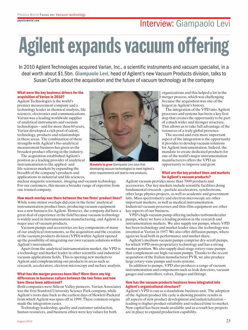
In 2010 Agilent Technologies acquired Varian, Inc., a scientific instruments and vacuum specialist, in a deal worth about $1.5bn. Giampaolo Levi, head of Agilent’s new Vacuum Products division, talks to
Susan Curtis about the acquisition and the future of vacuum technology at the company
Mandate to grow Giampaolo Levi says that developing vacuum technologies to meet Agilent’s strict requirements will lead to new products.
Agi
lent
Marketing and sales are also benefiting greatly from Agilent’s powerful corporate resources.
What impact has the merger had on product development?The need to develop vacuum solutions tailored to the strict specifications of Agilent Technologies is paying off in terms of the improvement of quality and reliability of all VPD products. This opportunity to further develop traditional Varian vacuum technology excellence will ultimately result in new market-leading products.
Where do you now see the major growth opportunities for the vacuum business? What new markets and applications are driving your product-development programme?Besides increasing our share in our core markets of research and instrumentation, we see opportunity for growth in thin-film coating, vacuum metallurgy and industrial leak-detection applications. Our acquisition of PVR has broadened our product offering in these markets. This addition completes the VPD product portfolio with a series of primary pumps suitable for backing high-vacuum turbo or diffusion pumps in various industrial applications.
What new technology developments are you working on to support your growth objectives?Recent breakthroughs include our new IDP dry-scroll pump, which employs an innovative hermetic design in which the motor and bearings are outside the vacuum space. This allows the complete isolation of all pumped gases. Other innovations in the IDP include a new single-layer tip seal, which makes the pumps
more tolerant to water vapour and other solvents. In high vacuum, an important recent innovation is our
TwisTorr turbo-pump technology. The pump’s new spiral drag stage enables a pump design that is at once very compact and able to sustain high gas flow and produce high compression ratios. The patented TwisTorr design ensures a constant local pumping speed inside the channel and avoids reverse pressure gradients, minimizing power consumption and improving the thermal performance of the pump.
In ultrahigh-vacuum ion pumps, recently our major focus has been on electronics – specifically designed control units, which maximize the pumping speed throughout the entire operating pressure range by automatically varying the high voltage as a function of pressure.
physicswor ld.com
Physics World Focus on: Vacuum technology
Interview: Giampaolo Levi
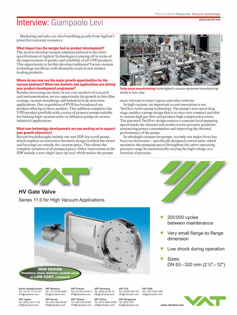
Turbo-pump manufacturing Inside Agilent’s vacuum-equipment manufacturing facility in Turin, Italy.
Agi
lent
VG SCIENTA
VG SCIENTA
Find Out More - www.vgscienta.com
Request a brochure - [email protected] Call sales support : +44 (0)1424 851291
Buy Online @ www.vgscienta.com/shop
Wide Bore Linear Transfer Mechanism
Wide Bore Omniax
Organic Deposition Devices
oC - 100oC in <70 mins
Global Innovators / Local Providers
EBARA Technologies, Inc.
Line & Valve Heaters
Repair & Remanufacturing Services
Parts Cleaning Services
24/7/365 Field Service
Rough Vacuum Pumps
High Vacuum Pumps
Exhaust Gas Abatement
Vacuum Valves & Hardware
www.ebaratech.com
800-535-5376
Augus t 2012 27
physicswor ld.com PumpingPhysics World Focus on: Vacuum technology
Nature abhors a vacuum. But that doesn’t stop us from trying, and when we succeed it opens up a vast array of new opportuni-ties. Dropping from atmospheric pressure (1013 mbar) to about 0.1 mbar, for example, is enough for the manufacture of compact fluorescent lamps, the freeze-drying of food and a range of other industrial processes.
Reducing the pressure further allows engineers to deposit high-quality materials with supreme precision. This makes possi-ble the semiconductor devices that are at the heart of all modern gadgets, anti-reflection and anti-bacterial coatings, and much more. At the extreme end of the vacuum scale, an almost perfect vacuum of 10–13 mbar is essential in high-energy physics to enable scientists to accelerate particles to very high speeds and then study their collisions.
Generating the appropriate vacuum con-ditions – and understanding what’s happen-ing inside the vacuum chamber – is crucial to the success of all applications of vacuum technologies. So let’s take a journey from normal atmospheric pressure down to extreme vacuum levels and examine the technology along the way.
Sweeping away gasScientists have been able to achieve pres-sures in the medium-vacuum regime, extending from 1 to 10–3 mbar, for hundreds of years. One of the most popular tech-niques remains the oil-sealed rotary-vane pump, which works on the principle of dis-placement. Gas flowing into the inlet port is trapped and compressed between a rotor vane and the pump’s body, from where it is swept towards the exhaust.
The oil in the pump plays several crucial roles: it lubricates the internal mechanical components; helps to dissipate heat; acts as a sealant that prevents gas from re-entering the vacuum chamber; and protects compo-nents from corrosive gases used in some deposition processes. However, it also has its downsides. “There is the potential for [oil] hydrocarbons streaming back from the inlet of the pump, which would contaminate the [vacuum] process,” explains Brandon Frid-
ley, product manager for pumps at vacuum specialist Kurt J Lesker. Fridley also points out that the oil must be replaced regularly, which leads to high maintenance costs.
Some of these problems can be overcome with dry pumps. Scroll pumps, for example, circle one spiral scroll around another, com-pressing the gas at the centre of the scroll, from where it is exhausted. “Over time you have some wear on components within certain models of dry pump that require replacement, but essentially they are main-tenance free,” says Fridley. However, dry pumps typically cost twice as much as their oil-sealed rivals and they typically deliver pressures 10 times higher.
Inside the chamberThese rotary and scroll pumps are some-times called “roughing pumps” because they can be used in the first stage of pump-ing a vacuum system from atmospheric pressure down to much lower pressures. Roughing pumps work best at medium vacuum levels where the large number of
gas molecules in the chamber ensures that the molecules constantly collide with each other. These collisions maintain the relative abundance of the different molecular spe-cies inside the chamber, which is similar to that at atmospheric pressure.
As the pressure drops below about 10–3 mbar, the average distance that a gas molecule travels before it collides with another molecule increases steadily from tens of nanometres to centimetres and beyond. As a molecule’s mean-free path starts to exceed the chamber’s dimensions, the molecules are more likely to hit the chamber wall than each other. At this stage the gas no longer flows like a liquid, and a simple roughing pump becomes ineffective.
Transferring momentumReducing the pressure further requires a pump that operates in a different way and one popular option is the turbomolecular pump. Turbo pumps work on a momentum transfer principle, in which gas molecules entering the pump are repeatedly kicked by a series of aluminium rotor blades moving between 20 000 and 90 000 rpm. The move-ment of the rotor blades accelerates the mol-ecules and steers them towards the exhaust.
“When you turn the turbo pump on, the roughing pump becomes a backing pump,” explains Fridley. “It continuously supports the turbo pump by pulling a sufficient vac-uum on the turbo pump’s exhaust.”
Another option is an oil-based diffusion pump, which must also be used in tandem with a backing pump. Diffusion pumps work by heating a low-vapour-pressure, high-molecular-weight oil stored in the base of the pump beyond its boiling point to form a dense vapour stream. This rises up a central column and out of conical noz-zles to form a “conical vapour curtain”. Any gas molecules entering the inlet of the pump collide with the oil curtain, bounce off towards the boiler and exit the pump. Oil is recycled during this process, because vapour hitting the water-cooled walls con-denses and returns to the boiler.
Reaching h igh-vacuum levels of 10–3–10–8 mbar is relatively straightforward using the right combination of pumps. How-ever, if the vacuum is needed for a produc-tion process, such as the coating of large sheets of glass, the pumping-down process must be fast enough to ensure high through-put and competitive manufacturing costs. Larger pumps extract gases more quickly, but care is needed to ensure that pumping does not lead to excessive cooling, which would cause condensation.
Using pumps alone to get pressures down to 10–8 mbar can take several weeks. Although molecular species such as nitro-gen, oxygen and carbon dioxide start to dis-appear below about 10–3 mbar, water vapour
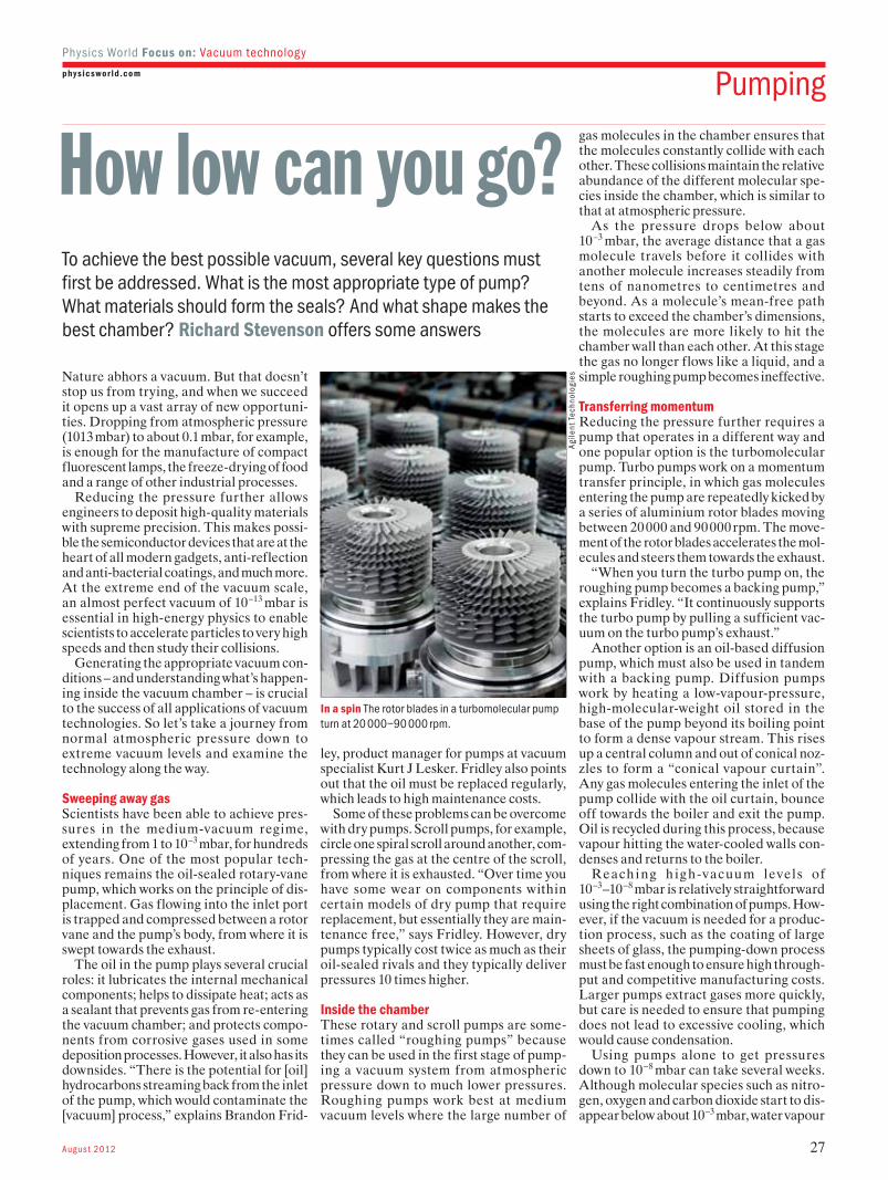
In a spin The rotor blades in a turbomolecular pump turn at 20 000–90 000 rpm.
Agi
lent
Tec
hnol
ogie
s
How low can you go?To achieve the best possible vacuum, several key questions must first be addressed. What is the most appropriate type of pump? What materials should form the seals? And what shape makes the best chamber? Richard Stevenson offers some answers
28 Augus t 2012
physicswor ld.com
Physics World Focus on: Vacuum technology
Pumping
is left behind to become the dominant spe-cies inside the chamber. Water is difficult to pump because the polarity of water mole-cules causes them to stick to the walls of the chamber – and the quickest way to remove them is to heat the chamber to about 150–200 °C for several hours. This “bake-out” process is done while the chamber is being pumped and evacuates most of the water, reducing the pressure to around 10–8 mbar.
At this stage most of the gas in the cham-ber is hydrogen, which is very difficult to pump. The mean-free path of the molecules is tens of kilometres, which means that almost all interactions occur on the cham-ber surfaces. Consideration must therefore be given to the design of the vacuum cham-ber and the materials inside it when creating ultrahigh-vacuum (UHV) conditions.
Indeed, achieving a UHV is more about reducing the amount of gas given off by materials inside the vacuum chamber – a process called outgassing – than it is about pumping. “Stainless steel is the most com-mon material [for building a chamber]. It is the easiest to work, and produces low levels of gas,” advises Paul Rummery, product manager for special fabrications at Kurt J Lesker, which offers a chamber-construction service. However, he explains that some grades of stainless steel are unsuitable, and that inferior suppliers may ship apparently ideal material that is porous under UHV conditions.
Shape of thingsThe shape of the chamber is also important for UHV – cylinders and spheres are far better at withstanding the pressure exerted by the atmosphere than are cubic shapes. As Rummery explains, this can lead to a trimming of material costs: “You can make a 300 mm diameter chamber out of 3 mm-thick material, but if you had a similar-sized 300 mm-sided box you would need 12–16 mm-thick material.”
It is also crucial to create high-quality welds using a material with minimal out-gassing properties. Metals – usually cop-per – are used as gaskets to make the seals between flanges. “The most common flange for ultrahigh vacuum has a knife edge that bites into the copper,” explains Rummery. If the vacuum demands are less severe, gaskets made from synthetic-rubber materials, such as Viton and buna-N, are popular choices.
Once the materials inside the cham-ber have been optimized, turbomolecular pumps can be used to reach UHV pres-sures of down to about 10–10 mbar, and even lower pressures if more than one are used in sequence. However, reaching pressures as low as 10–12 mbar requires an ion pump, which works by catching and holding mol-ecules, rather than removing them from the chamber. An ion pump contains a cloud of electrons that circle inside anode rings and are controlled by a strong magnetic field. When the electrons collide with gas mole-cules, they create positive ions that are then trapped by titanium cathode plates posi-tioned near the open ends of the anode rings.
At the extremeBeyond UHV lies extremely high vacuum. Particle accelerators, for example, require vacuum levels as low as 10 –13 mbar and achieving this involves a whole new level of innovation. An important challenge asso-ciated with accelerators is that an extreme vacuum must be created in the beam lines, which are long tubes with diameters of 25 mm or less. Removing gases from these tubes is an extremely time-consuming pro-cess that has been likened to draining the contents of a bath through a straw, rather than the plughole.
One of the most important recent devel-opments in this arena has been the use of non-evaporable getters (NEGs) inside accelerator beam lines. Getters are spe-cial materials that grab hold of gas mol-ecules and don’t let them go. The narrow tubes of an accelerator are coated with a thin layer of getter material, typically a titanium- zirconium-vanadium alloy. Heat-ing removes the oxide from the NEG, which enables it to trap carbon monoxide, carbon dioxide and hydrogen, the three most com-mon gases present in extremely low vacu-ums. Combining these coatings with a large and distributed vacuum system can gener-ate pressure levels as low as 10–13 mbar.
Designers of next-generation particle accelerators want to use even narrower cylinders, which will provide further chal-lenges for those designing future vacuum technologies. In particular, the develop-ment of thin-film getter coatings will con-tinue and the materials look set to drive vacuum systems to even lower pressures over the coming years.
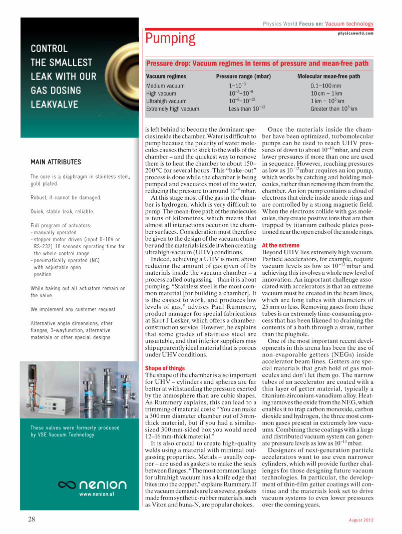
Vacuum regimes Pressure range (mbar) Molecular mean-free path
Medium vacuum 1–10–3 0.1–100 mmHigh vacuum 10–3–10–8 10 cm – 1 kmUltrahigh vacuum 10–8–10–12 1 km – 105 kmExtremely high vacuum Less than 10–12 Greater than 105 km
Pressure drop: Vacuum regimes in terms of pressure and mean-free path
ACCOMPLISHMENT VALUE EXPLORATION
PARTNERSHIP COMMUNITY INNOVATION NI C TO RM OM PIT PM UE SN T T D NE ES MIG PN O LIN EV VE EN DT I EON C NR AE MSE RA ORC RFH PEDelivering the latesttechnology inThin Film and NanoparticleSystems
www.mantisdeposition.com
30 Augus t 2012
Physics World Focus on: Vacuum technology
physicswor ld.com
Events Diary
2012European Conference on Surface Science (ECOSS-29)Edinburgh, Scotland3–7 SeptemberThis year ECOSS will be held alongside several other major condensed-matter conferences to provide a unique forum for researchers to present their work to a wider international audience. More than 1000 delegates from across the globe are expected to attend, including students, academics and industrial researchers, and a large exhibition will be run alongside the conference.
The programme will include plenary talks, invited and contributed presentations, and will allow ample time for poster sessions. A number of joint topical symposia have been scheduled
to enable surface scientists to exchange information with scientists working in other areas of condensed matter physics.www.cmd-24.org/home
13th International Conference on Plasma Surface EngineeringGarmisch-Partenkirchen, Germany 10–14 September This biennial conference will focus on the fundamentals and applications of plasma and ion-beam techniques in surface engineering. Organized by the European Joint Committee on Plasma and Ion Surface Engineering, the conference programme will range from fundamental plasma processes through to important applications in industrial manufacturing.
With numerous industrial exhibitors and some 30% of attendees expected to come from
industry, a special feature of PSE is the ability for research scientists to interact with engineers who are constantly looking for new solutions to emerging production challenges.www.pse-conferences.net/pse2012.html
Semicon EuropaDresden, Germany9–11 OctoberThe leading forum for semiconductor and microelectronics manufacturing in Europe, Semicon Europa is a key meeting place for buyers and sellers of vacuum technology. The event includes a large industry exhibition plus technical presentations and industry panels to help you keep up to date with key trends in semiconductor manufacturing.www.semiconeuropa.org
AVS 59th International Symposium and ExhibitionTampa, Florida, US28 October – 2 NovemberThis annual event in the vacuum calendar is expected to attract more than 2000 scientists and engineers to discuss everything from biotechnology through to nanoscience and novel materials and devices. Focus topics for this year’s meeting include electron transport in low-dimensional materials, graphene and related materials, in situ spectroscopy and microscopy, and nanomanufacturing science and technology.www2.avs.org/symposium
Vacuum Tech & Coating Expo 2012Milan, Italy7–9 NovemberThis event, billed as the most
Key meetings, conferences and exhibitions in the vacuum-technology calendar
Vacuum Expo 2012Coventry, UK17–18 OctoberCurrently the only event of its kind in the UK, this year’s Vacuum Expo will include a comprehensive industry exhibition plus a free two-day symposium to provide visitors with a full range of networking and training opportunities. Researchers and industry professionals will be able to discuss their technology needs with international suppliers of vacuum equipment and services, and will also be able to learn about emerging technologies, industry trends and applications of vacuum technology in science and industry.
For the second year running, the two-day Vacuum Symposium will run alongside the exhibition. Organized by the Institute of Physics’ Vacuum Group and the RGA Users Group, the first day of the symposium will focus on vacuum and plasmas for industry. The meeting will attempt to cover the wide range of industries that depend on plasma processing, which range from automotive and aerospace through to semiconductor manufacture and waste disposal. Speakers will explain the importance of plasmas in their industry, and one important topic for discussion will be how to eliminate contamination to avoid rejects and deliver maximum yield.
The second day of the Vacuum Symposium will feature a one-day meeting on
nanostructured metal-oxide thin films, which will cover deposition techniques and growth processes, characterization and properties, and integrated thin-film devices. The meeting aims to provide a forum for scientists and technologists working in different application areas to share knowledge, ideas and experiences.
“This research field is multidisciplinary, and widely dispersed among workers and users in a range of groups and subject areas,” says Zoe Barber of the University of Cambridge and a member the technical programme committee. “It’s essential that we get together, and a meeting such as nanostructured metal-oxide thin films is an ideal place to compare
approaches, find out about new ideas and challenges, and develop links.”
The conference will include invited speakers, contributed papers and a poster session, and will allow time for networking plus a visit to the exhibition. The call for papers remains open until 7 September, and the technical committee is particularly keen to see submissions in the following areas: transparent conducting oxides, optical layers, superconductors, displays, photocatalysis, water-vapour barriers and active electronic devices.
Delegates will also have access to an extensive pool of vacuum knowledge in the exhibition hall. A wide range of vacuum-related equipment will be on show, including a variety of pumping technologies, sample-handling systems, isolation valves and analytical instruments such as mass spectrometers and residual gas analysers. Power supplies and other electronics systems for vacuum systems will also be on display.
The event is held in conjunction with the Photonex exhibition at the Ricoh Arena in Coventry. Photonex is the UK’s largest event dedicated to optics, photonics and vision technologies, and also has an extensive conference programme. Key themes for this year’s conference include diode lasers, biophotonics, adaptive optics, and novel sources and detectors.www.vacuum-expo.com
32 Augus t 2012
physicswor ld.com
Physics World Focus on: Vacuum technology
physicswor ld.com
important European fair on vacuum and coating technologies, will include a rich conference programme alongside an industry exhibit featuring systems and components for a range of applications. It will once again form part of the wide-ranging HTE-hi.tech.expo trade show, where delegates can also explore the latest innovations in industry sectors such as photonics and lasers, batteries and charging systems, and magnets and superconductors.www.hitechexpo.eu/en_hte/index_hte.asp
MRS Fall Meeting and ExhibitBoston, US28 November – 2 DecemberThis regular meeting organized by the US-based Materials Research Society will highlight the extraordinary progress now being made in materials science and technology – much of which relies on vacuum processes. This year’s event will include 52 technical symposia organized into six broad themes.www.mrs.org/fall2012
2013VacuumTechExpo 2013Moscow, Russia16–18 AprilLeading companies such as Pfeiffer, Oerlikon and Vacom are expected to exhibit at this event, which runs alongside a research conference focused on vacuum equipment and technologies. The programme will include technical symposia and round-table discussions on the applications of vacuum equipment, materials and technologies in various industries.http://vacuumtechexpo.com
56th SVC Annual Technical ConferenceProvidence, US20–25 AprilThe 2013 SVC TechCon will explore the latest in vacuum coating and related technologies, as well as their role in high-tech applications. The programme will include technical presentations, an industry exhibit, a comprehensive education
programme, and a variety of networking events.
International Conference on Metallurgical Thin Films and Coatings (ICMCTF)San Diego, US23–27 AprilThe ICMCTF is the premier international event for thin-film deposition, characterization and advanced surface engineering. The conference, which this year celebrates its 40th anniversary, consistently attracts more than 700 scientists and engineers from industry, academia and government laboratories to discuss a compelling combination of cutting-edge research and real-world applications.
Key themes for the technical symposia include the development of new coating materials and processes, and evolving approaches for scaling up those processes for commercial applications. Running alongside the conference will be a two-day industrial exhibition, which will
showcase the latest equipment for the deposition, monitoring and characterization of coatings and thin films.www2.avs.org/conferences/icmctf
19th International Vacuum Congress (IVC-19)Paris, France9–13 SeptemberThe biggest vacuum event of them all, this time the IVC will be co-located with the International Conference on Nanoscience and Technology and the International Conference on Solid Surfaces, plus several other smaller events. Confirmed plenary speakers include Dan Shectman, who won the 2011 Nobel Prize for Chemistry for his discovery of quasicrystals, and delegates will be spoilt for choice with around 2000 presentations expected to run in 15 parallel sessions.
The programme also includes an industry exhibit and short courses delivered by industry experts.www.ivc19.com
Events Diary
Bringing Together the Best in Vacuum Coating and Surface Engineering Technologies
2013 TechCon DatesTechnical Program April 22–25
Technology Exhibit April 23–24
Education Program April 20–25
Join the Society of Vacuum Coaters in the heart of New England’s “Technology Corridor” for the 56th Annual Technical Conference, Exhibit, Education Program and Networking events.
The 2013 TechCon will feature the following Symposia:
These and other topics will be explored in our traditional Technical Sessions. Abstract Submission Deadline: October 12, 2012
Society of Vacuum Coaters www.svc.org

HiCube™ Pro
� Modular pumping station for clean vacuum� Dry, multi-stage ACP roots pump� High performance turbopump with integrated drive� Robust engineering makes for long service life and high reliability
Are you looking for a perfect vacuum solution? Please contact us:
Pfeiffer Vacuum GmbH · Headquarters/Germany T +49 6441 802-0 · F +49 6441 802-1202 [email protected]
www.pfeiffer-vacuum.com
A P A S S I O N F O R P E R F E C T I O N
The complete Solution for High Vacuum Applications
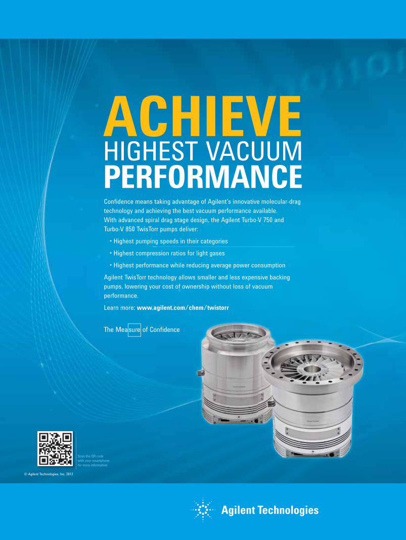
© Agilent Technologies, Inc. 2012
ACHIEVEHIGHEST VACUUMPERFORMANCE
Scan the QR codewith your smartphonefor more information
Confidence means taking advantage of Agilent’s innovative molecular-dragtechnology and achieving the best vacuum performance available.With advanced spiral drag stage design, the Agilent Turbo-V 750 andTurbo-V 850 TwisTorr pumps deliver:
Agilent TwisTorr technology allows smaller and less expensive backingpumps, lowering your cost of ownership without loss of vacuumperformance.
Learn more: www.agilent.com/chem/twistorr