Embed Size (px)
Citation preview

A32
FMJ A32, P35 & P35/3Amplifi ers
Service Manual
ARCAMARCAM
Issue 1.0
Contents List
! Phono board L870
o Circuit description o Component overlay o Parts list o Circuit diagrams
! Amplifier & PSU board L882
o Circuit description o Component overlay o Parts list o Circuit diagrams
! Display board L928
o Component overlay o Parts list o Circuit diagrams
! Preamplifier board L937
o Circuit description o Component overlay o Parts list o Circuit diagrams
! 3rd Channel Amplifier board L911 o Component overlay o Parts list o Circuit diagrams
! Transformer specifications o L914TX o L915TX
! General assembly
o A32 - Mechanical parts list o P35 - Mechanical parts list o P35/3 - Mechanical parts list
Phono Board L870
Contents
! Circuit description
! Component overlay
! Parts list
! Circuit diagrams

AV8 Phono Board Circuit Description Refer to circuit diagram L870 sheet 1 The phono board is a simple single stage RIAA amplifier and consists of two channels of high gain amplification, and the ability to switch between moving magnet (MM) and moving coil (MC) settings. PSU The unit derives its + 15V regulated rails from the unit it is fitted into with only local decoupling capacitors on board. Interface The unit connects to the host unit via a 8 way connector. Amplification The left channel has designators beginning with 100, and the right with 200. For the purposes of this description the left channel will be described, as the right channel is the same in all respects. The amplifier is a small signal class A voltage feedback amplifier with switch able gain. The input consists of an actively loaded differential pair of very low noise PNP transistors (TR106, TR107). These transistors are very specific and should only be replaced with identical parts with the E grade high gain. TR100 and TR101 form a current source for the pair, which sets the quiescent current for the entire amplifier. The active load consists of TR110 and TR111, which forms part of the differential current mirror with TR112, TR113 & TR114. This differential stage also has an active load (TR102 & TR103) to keep gain to a maximum. Both of these differential stages are designed to have as much gain as possible to enable the single stage design. The RIAA response is achieved in the feedback network: C101, C110, C111, C112, C119, C120 and R115, R112. C115 is used to correct between MM and MC gains as the amplifier is non-inverting. SW100 switches between MM and MC. Two poles of the switch change between the different loading required for each type of the cartridge: R108 & C109 for MM and added in parallel for MC R104 & C108. The other two poles change the feedback resister value to alter the gain: R105 for MM and added in parallel for MC R123. The DC offset is controlled by a non-inverting servo built around IC100. The amount of servo current is different for each gain setting via R111 (MM) and R124 (MC) so that the low frequency high pass point remains the same for both settings. However the high pass point for the circuit is set by C113. This gives a warp filter, stops DC start-up thumps from upsetting DC coupled circuitry and an approximation of the RIAA/IEC curve (-2dB @ 20Hz) The output is class A buffered by a dual mirror follower (TR104, TR105, TR108, TR109). The quiescent current is set by D100 and R118 and R119. Closed loop stability is achieved with C16, C117, giving symmetrical slewing capability.
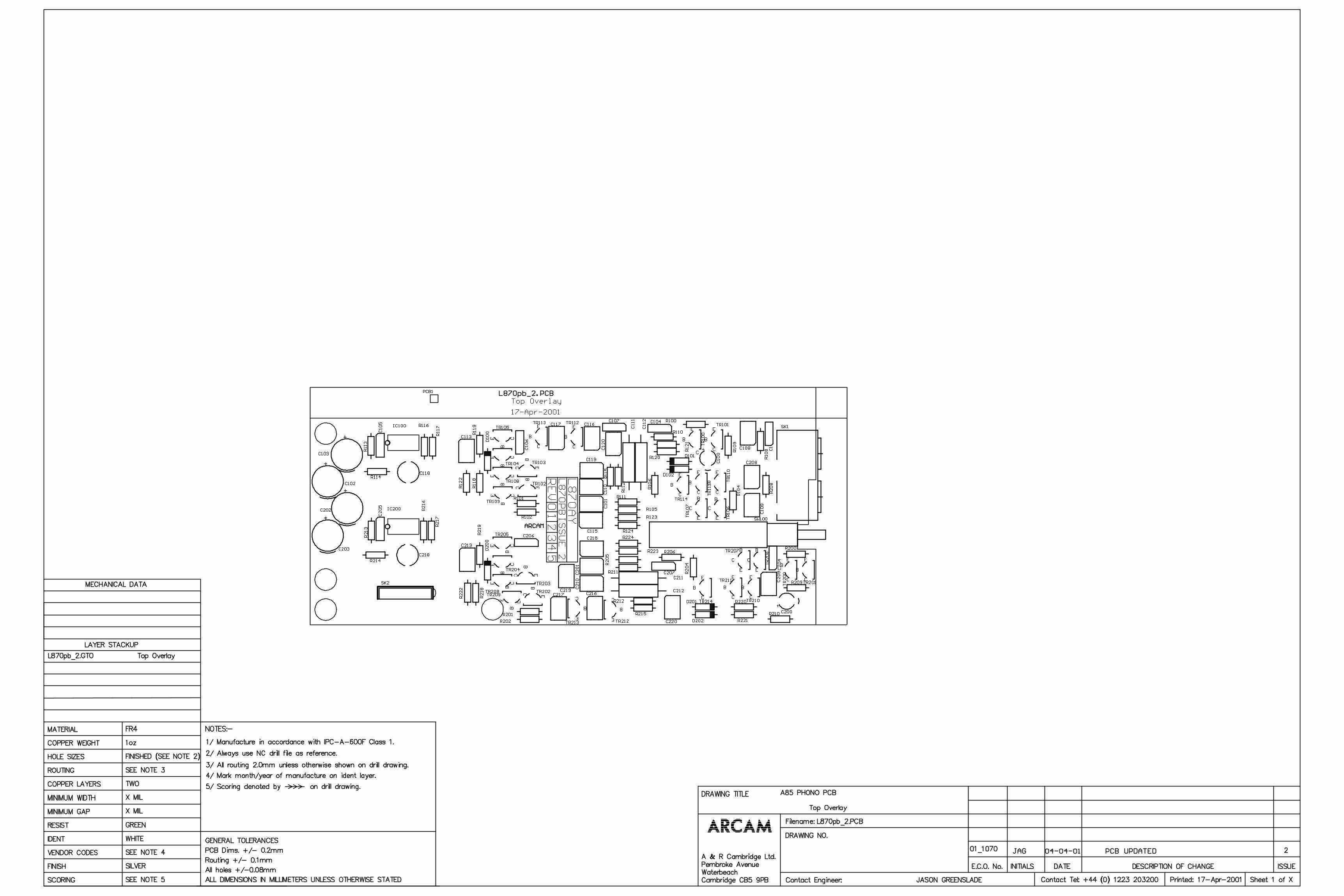
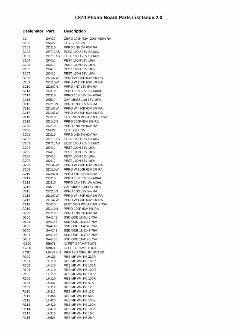
L870 Phono Board Parts List Issue 2.0
Designator Part Description
C1 2A410 CERD 100N 63V -20% +80% RAC100 2N622 ELST 22U 63VC101 2D210 PPRO 1N0 5% 63V RAC102 2P710AS ELEC 100U 25V SILMICC103 2P710AS ELEC 100U 25V SILMICC104 2K410 PEST 100N 63V 10%C105 2K410 PEST 100N 63V 10%C106 2K410 PEST 100N 63V 10%C107 2K410 PEST 100N 63V 10%C108 2D147W PPRO W 470P 63V 5% RAC109 2D110W PPRO W 100P 63V 5% RAC110 2D247N PPRO 4N7 63V 5% RAC111 2D310 PPRO 10N 63V 1% AXIALC112 2D310 PPRO 10N 63V 1% AXIALC113 2K510 CAP MKS2 1U0 16V 10%C115 2D213N PPRO 1N3 63V 5% RAC116 2D147W PPRO W 470P 63V 5% RAC117 2D147W PPRO W 470P 63V 5% RAC118 2U610 ELST NON POLAR 10UF 35VC119 2D110N PPRO 100P 63V 5% RAC120 2D210 PPRO 1N0 5% 63V RAC200 2N622 ELST 22U 63VC201 2D210 PPRO 1N0 5% 63V RAC202 2P710AS ELEC 100U 25V SILMICC203 2P710AS ELEC 100U 25V SILMICC204 2K410 PEST 100N 63V 10%C205 2K410 PEST 100N 63V 10%C206 2K410 PEST 100N 63V 10%C207 2K410 PEST 100N 63V 10%C208 2D147W PPRO W 470P 63V 5% RAC209 2D110W PPRO W 100P 63V 5% RAC210 2D247N PPRO 4N7 63V 5% RAC211 2D310 PPRO 10N 63V 1% AXIALC212 2D310 PPRO 10N 63V 1% AXIALC213 2K510 CAP MKS2 1U0 16V 10%C215 2D213N PPRO 1N3 63V 5% RAC216 2D147W PPRO W 470P 63V 5% RAC217 2D147W PPRO W 470P 63V 5% RAC218 2U610 ELST NON POLAR 10UF 35VC219 2D110N PPRO 100P 63V 5% RAC220 2D210 PPRO 1N0 5% 63V RAD100 3A4148 SSDIODE 1N4148 75VD101 3A4148 SSDIODE 1N4148 75VD102 3A4148 SSDIODE 1N4148 75VD200 3A4148 SSDIODE 1N4148 75VD201 3A4148 SSDIODE 1N4148 75VD202 3A4148 SSDIODE 1N4148 75VIC100 5B071 IC FET OPAMP TL071IC200 5B071 IC FET OPAMP TL071PCB1 L870PB_2 PRINTED CIRCUIT BOARDR100 1H133 RES MF W4 1% 330RR101 1H110 RES MF W4 1% 100RR102 1H110 RES MF W4 1% 100RR104 1H110 RES MF W4 1% 100RR105 1H110 RES MF W4 1% 100RR106 1H110 RES MF W4 1% 100RR108 1H347 RES MF W4 1% 47KR109 1H312 RES MF W4 1% 12KR110 1H312 RES MF W4 1% 12KR111 1H356 RES MF W4 1% 56KR112 1H410 RES MF W4 1% 100KR113 1H410 RES MF W4 1% 100KR114 1H410 RES MF W4 1% 100KR115 1H315 RES MF W4 1% 15KR116 1H522 RES MF W4 1% 2M2
L870 Phono Board Parts List Issue 2.0
Designator Part Description
R117 1H522 RES MF W4 1% 2M2R118 1H022 RES MF W4 1% 22RR119 1H022 RES MF W4 1% 22RR120 1H022 RES MF W4 1% 22RR121 1H022 RES MF W4 1% 22RR122 1H339 RES MF W4 1% 39KR123 1H010 RES MF W4 1% 10RR124 1H256 RES MF W4 1% 5K6R200 1H133 RES MF W4 1% 330RR201 1H110 RES MF W4 1% 100RR202 1H110 RES MF W4 1% 100RR204 1H110 RES MF W4 1% 100RR205 1H110 RES MF W4 1% 100RR206 1H110 RES MF W4 1% 100RR208 1H347 RES MF W4 1% 47KR209 1H312 RES MF W4 1% 12KR210 1H312 RES MF W4 1% 12KR211 1H356 RES MF W4 1% 56KR212 1H410 RES MF W4 1% 100KR213 1H410 RES MF W4 1% 100KR214 1H410 RES MF W4 1% 100KR215 1H315 RES MF W4 1% 15KR216 1H522 RES MF W4 1% 2M2R217 1H522 RES MF W4 1% 2M2R218 1H022 RES MF W4 1% 22RR219 1H022 RES MF W4 1% 22RR220 1H022 RES MF W4 1% 22RR221 1H022 RES MF W4 1% 22RR222 1H339 RES MF W4 1% 39KR223 1H010 RES MF W4 1% 10RR224 1H256 RES MF W4 1% 5K6SK1 8D230 PHONO SKT 2-WAY HOR EMC GOLDSK2 8K2408 8-WAY AMP CT CONNSW100 A1013 SW PUSH 4PCOTR100 4A556 TRANS LF SS P BC556BTR101 4A556 TRANS LF SS P BC556BTR102 4A556 TRANS LF SS P BC556BTR103 4A556 TRANS LF SS P BC556BTR104 4A556 TRANS LF SS P BC556BTR105 4A556 TRANS LF SS P BC556BTR106 4A1085 TRANS LF SS P 2SA1085TR107 4A1085 TRANS LF SS P 2SA1085TR108 4A546 TRANS LF SS N BC546BTR109 4A546 TRANS LF SS N BC546BTR110 4A546 TRANS LF SS N BC546BTR111 4A546 TRANS LF SS N BC546BTR112 4A546 TRANS LF SS N BC546BTR113 4A546 TRANS LF SS N BC546BTR114 4A546 TRANS LF SS N BC546BTR200 4A556 TRANS LF SS P BC556BTR201 4A556 TRANS LF SS P BC556BTR202 4A556 TRANS LF SS P BC556BTR203 4A556 TRANS LF SS P BC556BTR204 4A556 TRANS LF SS P BC556BTR205 4A556 TRANS LF SS P BC556BTR206 4A1085 TRANS LF SS P 2SA1085TR207 4A1085 TRANS LF SS P 2SA1085TR208 4A546 TRANS LF SS N BC546BTR209 4A546 TRANS LF SS N BC546BTR210 4A546 TRANS LF SS N BC546BTR211 4A546 TRANS LF SS N BC546BTR212 4A546 TRANS LF SS N BC546BTR213 4A546 TRANS LF SS N BC546BTR214 4A546 TRANS LF SS N BC546B
1 2 3 4 5 6 7 8
A
B
C
D
87654321
D
C
B
A
ISSUE
DRAWING NO.
23425
DRAWING TITLE
Drawn by:DATE
FilenameECO No. DESCRIPTION OF CHANGE
G:\DATA\ECO\ECO AGENDA\01_1070 l870 A85 PHONO ISSUE2\L870_2.0.ddb - L870c1_2.0.PRJ
A & R Cambridge Ltd.Pembroke AvenueDenny Industrial CentreWaterbeachCambridge CB5 9PB
A85 PHONO STAGE - TOP LEVEL
Circuit Diagram
L870C1JBR23-Apr-2001
INITIALSDate Printed 1 3Sheet of
Notes:
1
EMC
SK1PHONO2HG
0V_SIG
0V_SIG
LEFT IN LEFT OUT
LEFT CHANNELL870C2_2.0.SCH
RIGHT IN RIGHT OUT
RIGHT CHANNELL870C3_2.0.SCH
12345678
SK2
AMPCT8
+15V
-15V
0V_HF0V_SIG
Q_1
Q_2
Q_3
Q_4
Q_5
Q_6
Q_7 Q_8
PCB
PCB1
L870PB_2
Update Box
EL1
UPDATE_BOX
C1100N CD
00_1051 JAG 22/3/01 PRODUCTION ISSUE 1
01_1070 JAG 17/4/01 updated pcb and scm 2
1 2 3 4 5 6 7 8
A
B
C
D
87654321
D
C
B
A
ISSUE
DRAWING NO.
23425
DRAWING TITLE
Drawn by:DATE
FilenameECO No. DESCRIPTION OF CHANGE
G:\DATA\ECO\ECO AGENDA\01_1070 l870 A85 PHONO ISSUE2\L870_2.0.ddb - L870C2_2.0.SCH
A & R Cambridge Ltd.Pembroke AvenueDenny Industrial CentreWaterbeachCambridge CB5 9PB
A85 PHONO STAGE - LEFT CHANNEL
Circuit Diagram
L870C2JBR23-Apr-2001
INITIALSDate Printed 2 3Sheet of
Notes:
TR1062SA1085
TR1072SA1085
R12022R MF
R12122R MF
R105100R MF
R10847K MF
R101100R MF
R102100R MF
+ C102100U SILMIC
+C103100U SILMIC
R100330R MF
+ C10022U EL
R10912K MF
R11012K MF
C105100N PE
R117
2M2 MFR111
56K MF
R113100K MF
R114100K MF
TR111BC546B
TR110BC546B
TR114BC546B
TR112BC546B
TR113BC546B
TR100BC556B
TR101BC556B
TR102BC556B
TR103BC556B
TR104BC556B
TR105BC556B
TR108BC546B
TR109BC546B
+15V
-15V
R12239K MF
R112
100K MF
R115
15K MF
456
SW100B4PCO
10 11 12
SW100D4PCO
R104100R MF C108
470P PPW R12310R MF
C104100N PE
C107100N PE
R116
2M2 MF
3
26
74
IC100
TL071CD
0V_SIG0V_SIG
D1001N4148
R11822R MF
R11922R MF
C106100N PE
0V_SIG0V_HF
0V_SIG
0V_SIG0V_HF
D1011N4148
D1021N4148
R106100R MF
LEFT IN
LEFT OUT
Q_101
Q_102
Q_103
C109100P PPW
R1245K6 MF
C117470P PPWC116
470P PPW
C111
10N PP AX
C112
10N PP AX
C118
10U NP
C113
1U0 PE
C1151N3 PP
C110
4N7 PP
C101
1N0 PP
C119
100P PP
00_1051 JAG 22/3/01 PRODUCTION ISSUE 1
C120
1N0 PP
01_1070 JAG 17/4/01 updated pcb and scm 2

1 2 3 4 5 6 7 8
A
B
C
D
87654321
D
C
B
A
ISSUE
DRAWING NO.
23425
DRAWING TITLE
Drawn by:DATE
FilenameECO No. DESCRIPTION OF CHANGE
G:\DATA\ECO\ECO AGENDA\01_1070 l870 A85 PHONO ISSUE2\L870_2.0.ddb - L870C3_2.0.SCH
A & R Cambridge Ltd.Pembroke AvenueDenny Industrial CentreWaterbeachCambridge CB5 9PB
A85 PHONO STAGE - RIGHT CHANNEL
Circuit Diagram
L870C3JBR23-Apr-2001
INITIALSDate Printed 3 3Sheet of
Notes:
TR2062SA1085
TR2072SA1085
R22022R MF
R22122R MF
R205100R MF
R20847K MF
R201100R MF
R202100R MF
+ C202100U SILMIC
+C203100U SILMIC
C209
100P PPW
R200330R MF
+ C20022U EL
R20912K MF
R21012K MF
C205100N PE
R217
2M2 MFR211
56K MF
R213100K MF
R214100K MF
TR211BC546B
TR210BC546B
TR214BC546B
TR212BC546B
TR213BC546B
TR200BC556B
TR201BC556B
TR202BC556B
TR203BC556B
TR204BC556B
TR205BC556B
TR208BC546B
TR209BC546B
+15V
-15V
R22239K MF
R212
100K MF
R215
15K MF
123
SW100A4PCO
7 8 9
SW100C4PCO
R204100R MF
C208
470P PPWR22310R MF
C204100N PE
C207100N PE
R216
2M2 MF
3
26
74
IC200
TL071CD
0V_SIG0V_SIG
D2001N4148
R21822R MF
R21922R MF
C206100N PE
0V_SIG0V_HF
0V_SIG
0V_SIG0V_HF
D2011N4148
D2021N4148
R206100R MF
RIGHT IN
RIGHT OUT
Q_201
Q_202
Q_203
R2245K6 MF
C217470P PPWC216
470P PPW
C215
1N3 PP
C211
10N PP AX
C212
10N PP AX
C21810U NP
C213
1U0 PE
C219
100P PP
C210
4N7 PP
C201
1N0 PP
00_1051 JAG 22/3/01 PRODUCTION ISSUE 1
C220
1N0 PP
01_1070 JAG 17/4/01 updated pcb and scm 2
Amplifier + PSU
Board L882
Contents
! Circuit description
! Component overlay
! Parts list
! Circuit diagrams
Amplifier & PSU Circuit Description Refer to L882 circuit diagrams This is the printed circuit board that provides the power supply and output stage amplifiers for the A32 integrated and P35 power amplifiers. Its function is to: ! Drive the loudspeakers ! Provide an (always on) auxiliary 5VDC supply for the
micro controller and display interface ! Receive logic signals from the micro controller to turn
on the main amplifier supply relay (mains) and connect either pair of speaker output sockets
! Send logic signals to the micro controller pertaining to the state of the amplifiers (short circuit protection, DC offset protection, thermal protection)
! Receive and demodulate RC5 remote style control codes via the rear panel jack and transmit them to the micro controller
! Send a 12V trigger output via the rear panel jack for control of an auxiliary power amp when the unit is on
! Receive a 12V trigger input from the rear jack (for use in the power amp only version)
! Drive a pair of headphones via attenuating resistor networks The power amplifier is a symmetrical, class B, bipolar junction transistor output, current-feedback design (of which more later) with DC-coupled signal and feedback paths, featuring an active integrating voltage servo to control DC offsets.
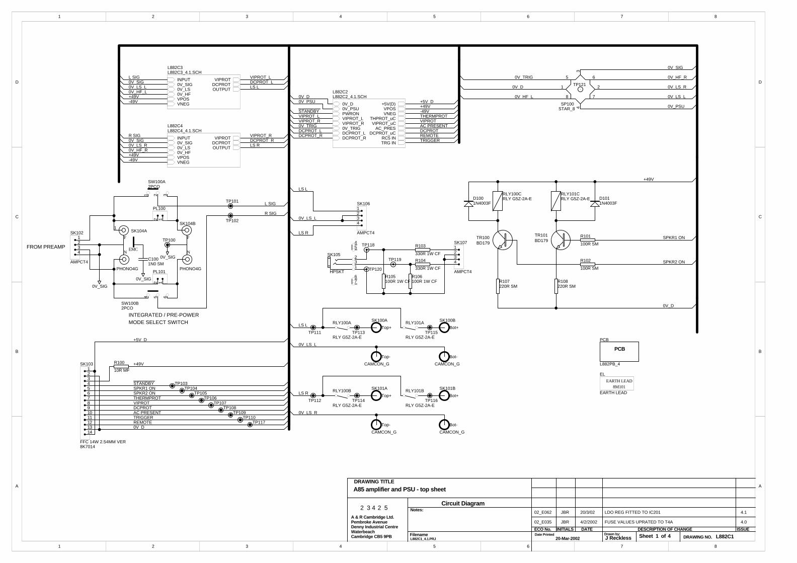
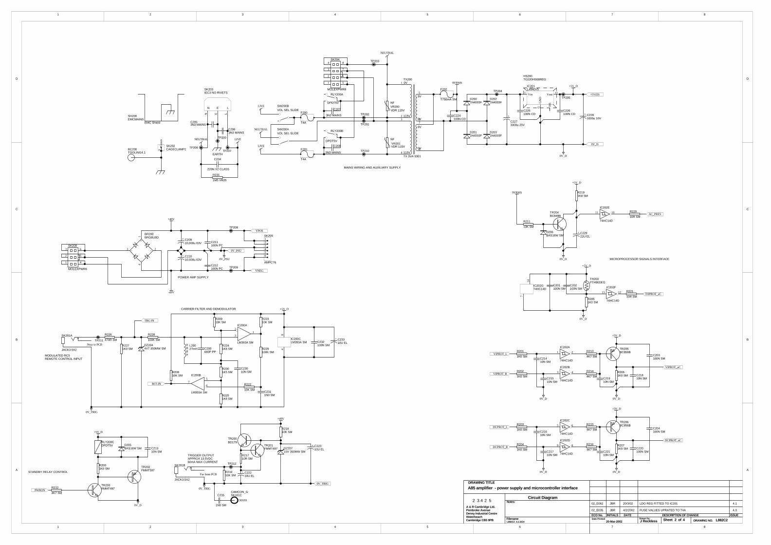
It features ‘instantaneous’ safe operating area protection in addition to sending a signal to the micro to turn off the output relays in the event of user or thermal overload. Since it is a DC-coupled design, the unit senses DC at the output and triggers the micro to turn off the loudspeaker relays in the event of excessive levels (possibly due to a faulty source component or short circuit output transistor). The output stage uses Sanken specialised ‘audio amplifier’ power bipolar Darlington transistors which are optimised for use with this type of topology. Consequently the unit has excellent measured performance in terms of noise, slew rate, output impedance and distortion (harmonic and intermodulated) and is essentially load invariant (to a first order the measured performance is independent of the load impedance). L882 Circuit Sheet 1 The audio input to the amplifier is connected to SK102 (which connects to the output of the preamp PCB). This signal is passed on via SK104A which forms the preamp out connection to the outside world. SK104B provides the power amp input connection, with switchSW100 selecting between pre / power and integrated modes. The unit is wired as a preamp / power amp combination with the switch depressed, allowing the user to insert a processor or other function (e.g. graphic EQ) between the output of the preamp and the input of the power amp. With the switch in the ‘out’ position the power amp input socket is ignored and the input to the power amp is connected internally to the output of the preamp. PL100 and PL101 are ‘handbag’ links fitted to the power amp only version to connect both pairs of phono sockets in parallel for daisy chaining (as there is no preamp output on a power amp). Relays RLY100 and RLY101 switch the two pairs of loudspeaker output sockets and are controlled by the micro lines describes above. Transistors TR100 and TR101 operate in ‘constant current sink’ mode which allow relay current to be approximately constant although the main power supply
rails will vary with mains input and load conditions. The current is around 20mA per relay. Star point SP100 is the ground ‘mecca’ for the entire amplifier (comprising all three PCBs within the unit). All of the separately named grounds are joined explicitly at this point. Different named grounds are used to ensure that no two ‘different’ grounds share copper, which could compromise the noise, distortion or crosstalk performance of the amplifier. The loudspeaker output signals are passed to socket SK106 which connects to SK107 and onto the headphone output via the attenuation resistors R103 thru R106. The hierarchy containing the other sheets is self explanatory. Each of the port names shown on the top sheet connects to the port of the same name on the lower sheets. L882 Circuit Sheet 2 This sheet contains the power supplies, the rear panel jack socket trigger circuits, the standby relay control and the ‘interface’circuits between the output signals of the power amplifiers and the inputs expected by the micro processor. The mains input enters the unit at SK203, with capacitors C205 and C206 acting as conducted RF suppression. The earth connection is passed on to the chassis (for safety reasons the chassis metalwork remains connected to mains power earth at all times). Switch SW200 is the voltage selector switch, allowing the unit to be operated in 230V or 115V mains countries by switching the dual-primary mains transformers between series and parallel winding. Varistors VR200 and VR201 act to prevent over-voltage surges from damaging the unit. If the user selects 115V operation and then connects the unit to a 230V supply, the varistors will go to a low impedance and blow the primary fuses. Any very high voltage line transients will also be suppressed, helping to eliminate transformer isolation breakdown. Relay RLY200 switches the primary side of the mains transformer, allowing the micro to control the on / off status of the amplifier. Its contacts are snubbed by capacitors C207 and C208 (to eliminate switching spark transients and prolong relay lifespan). The primary windings of the toroidal mains transformer connect to SK204. PCB mounted transformer TX200 is powered all the time that mains is present on SK203, irrespective of the on / off status of the amplifier. This is to ensure that the micro processor is always operational and can thus control the mains switching for the main amplifier. Secondary fuse F202 limits the current in the event of a failure mode, as the short circuit primary current of TX200 would be insufficient to blow the mains fuses. Diodes D200 thru D203, C227 and IC201 provide the 5VDC supply which powers the micro and display PCB and the relay coils. C224 is to reduce diode noise being transmitted back through the leakage capacitance of TX200. The mains transformer secondary winding is connected to SK200. This is a centre tapped winding, and is used with full bridge rectifier BR200 to produce the main positive and negative supplies for the power amp. C209 and C210 are the large reservoir capacitors, with C211 and C212 acting as high frequency decouplers. The main power supply rails and ground are accessible on SK205 for future module expansion.
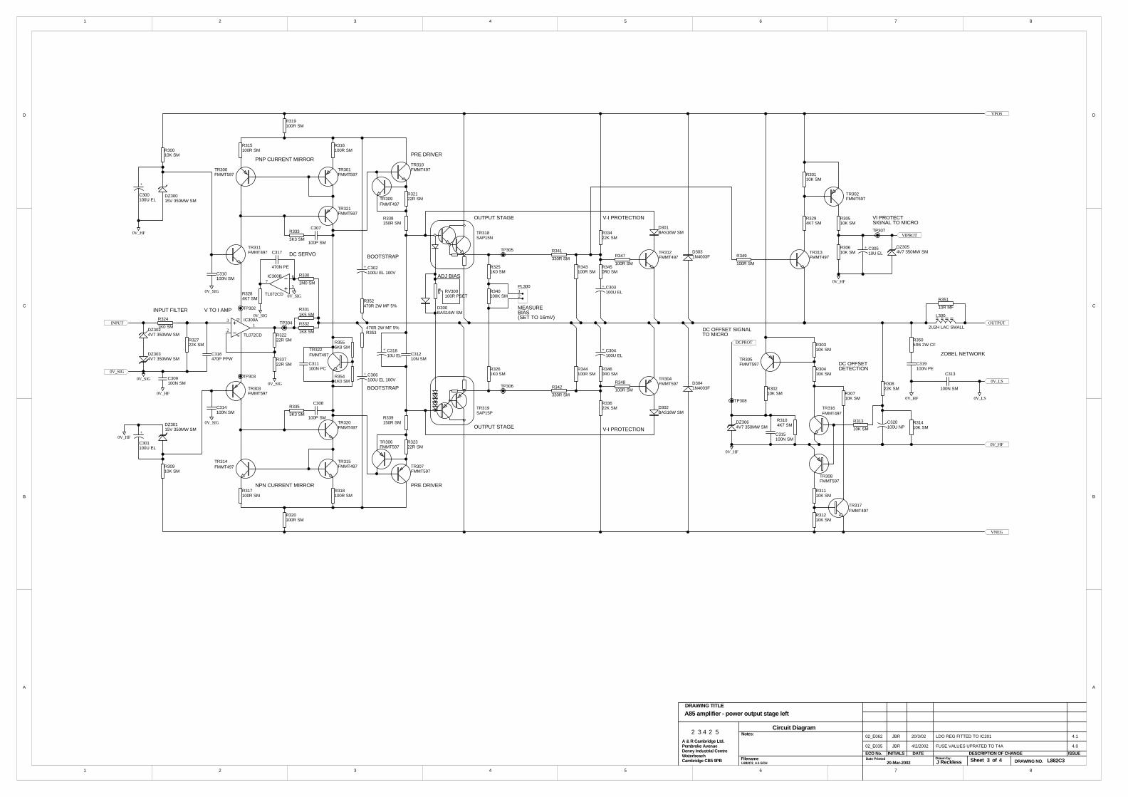
The circuitry around SK201A and IC200 is to receive and demodulate remote control commands sent in via the rear panel jack socket. This is for multi-room applications. L200 and C200 form a parallel resonant circuit at approximately 37kHz. The output from this bandpass filter is passed into IC200A where it is ‘chopped’ and fed to IC200B to provide the output signal. SK201B is a 13VDC signal trigger output which is active whenever the amplifier is powered up. R218 and DZ207 / C223 provide a reference voltage which is buffered by TR200. TR201 and R217 act as a current limit and prevent damage due to a short circuit on the output of SK201B. The maximum current is approximately 65mA. TR203 and TR202 are a complementary Darlington pair which turn on mains relay RLY200 when activated by a signal from the microprocessor. TR204 and its associated components are to detect whenever AC mains is present at the IEC socket. This is to notify the microprocessor if the user has unplugged the mains cord, so that it can take the necessary action (muting all the outputs and switching off the mains relay). The reservoir capacitors should last at least 4 mains cycles which gives the microprocessor plenty of time for a controlled shutdown. TR204 forms a monostable circuit. Each cycle of AC turns on TR204 via R211. TR204 then ‘shunts’ C229 ensuring that it is kept at a low potential. If more than one mains cycle is missing, then R219 charges up C229 sufficiently to trigger Schmitt inverter IC202E thus passing on a logic signal to the microprocessor. The use of a Schmitt inverter for IC202 is to ensure that the micro receives ‘clean’ logic levels - the hysteresis voltage (about 0.5V) is sufficient to prevent circuit noise from producing a string of ‘ghost’ signals when analogue levels are near the threshold point. TH200 is a positive tempco thermistor placed adjacent to the heatsink on which the output transistors are mounted. When the temperature of the thermistor exceeds 90 degrees Celsius the thermistor goes to a high impedance and so the input to IC202F goes low. This triggers a HIGH output to the micro indicating thermal overload. The VI protection signals from the left and right channels pass into IC202A and IC202B respectively, to be ‘cleaned up’ via the Schmitt trigger. They are then NOR’d using TR205 which sends a HIGH signal to the micro in the event of either channel suffering a short circuit or current overload. Exactly the same approach is used for the DC fault lines using IC202C and IC202D. L882 Circuit Sheet 3 This is the main audio power amplifier circuit. The amplifier is a class B design, which uses SAP ‘audio’ transistors in a symmetrical current feedback configuration. Input and feedback paths are DC coupled and there is an active integrating servo to remove DC offsets from the output. The basic principle of operation is follows: The input signal is amplified by a factor of 2 in IC300A. This drives a 44˜ impedance to ground causing the supply pin currents to change with the signal level. These changing supply pin currents are then ‘reflected’ by a pair of complementary Wilson mirrors and passed on to a series of buffer transistors before being connected to the load. The ‘feedback current’ flows back from the output terminal via R331 and R332 and attempts to provide the current necessary to allow IC300A to swing its output without drawing excessive current from its supply pins, thus making the change in supply current very small indeed. This is why the term ‘current feedback’ is used - it is the current flowing in
the feedback resistors that sets the overall gain of the amplifier. IC300B acts as an inverting integrator and its purpose is to remove DC from the loudspeaker output. Any positive DC offset will cause the output of IC300B to go negative, thus increasing the current in its negative supply pin and pulling the output voltage back towards zero. R330 and C317 set the time constant of this integrator (0.47 seconds) so that audio frequency components are ignored and only DC and subsonic frequencies are removed. The input to the amplifier is limited to ±5.4V via back-to-back zener diodes DZ302 and DZ303. This is to prevent the user from grossly overdriving the input to the amplifier and possibly causing damage. The diodes appear before series resistor R324 so that their variable capacitance does not introduce high frequency harmonic distortion. R324, R327 and C316 act as an input filter - this is a first order low pass filter with a corner frequency of around 340kHz to prevent RF signals from being injected into the front end of the amplifier. The corner frequency was chosen such that the phase shift introduced is less than 5˜ at 20kHz (considered by the AES to be the minimum perceptible relative amount by the human ear). The input impedance of the amplifier is 23kW at DC, falling to around 14kW at 20kHz. Operational amplifier IC300A is acting as a non-inverting gain of 2, driving the input signal into a 44W impedance to ground via R322 and R337. Its output voltage will be an accurate amplification of its input voltage (i.e. the signal on pin 1 should look identical to that on pin 3 but at twice the amplitude). The op-amp is used in a slightly unusual configuration here, in that its power supply pins are used as a (current) output, and its output pin is used as a (current) feedback. Transistors TR311 and TR303 supply the ±15V rails to the op-amp, and act as cascades to pass its supply pin currents through to the current mirrors, which sit at a potential too high for the op-amp to be connected directly. TR300, TR301 and TR321 form a PNP Wilson current mirror, which reflects the current sunk by the positive supply pin of IC300. Likewise TR314, TR315 and TR320 form an NPN Wilson current mirror, which reflects the current sourced by the negative supply pin of IC300. R315 thru R318 provide emitter degeneration of approximately 300mV for the current mirrors (as they pass about 3mA DC in quiescent conditions), to ensure accurate operation independent of the small variations between the transistors in the current mirrors. They also ensure that the current passing down the next stage is reasonably constant as the internal temperature of the amplifier changes, swamping out small thermal variations in the VBE of the mirror transistors. R319 and R320 slightly decouple the rails to the current mirrors from the main power rails of the amplifier, to allow the bootstrap circuit to operate. The bootstrap consists of C302 and C306 with metal film power resistors R352 and R353. The bootstrap is provided to allow the power supply rails of the current mirrors to go up and down slightly with the output signal into the loudspeaker. This enables the driver stage to fully saturate the output transistors and thus give the greatest power output and best thermal efficiency for any given power rail voltage. The voltage on the ‘inside’ end of R319 and R320 will vary by about 12 volts peak to peak at full output power, rising above the main power rails during signal peaks.
C307 and C308 with R333 and R335 provide the compensation necessary to ensure stability when the loop is closed. They are Miller capacitors which dramatically reduce the transimpedance (i.e. current to voltage gain) of the current mirrors at high frequencies. The present value of 47pF provides for a unity gain open loop bandwidth of around 75MHz, whilst ensuring a closed loop gain margin of around 6dB (note that gain margin in a current feedback design is not dependent on system bandwidth to a first order approximation). R333 and R335 provide a ‘zero’ in the open loop frequency response which is tailored to give the best time domain performance (i.e. to make high frequency square waves look square with minimal ringing or overshoot). DZ304 and C311 provide a fixed 4.7V bias voltage to allow the following stages to operate correctly. C311 is there to ensure that both halves of the following stage receive an equal AC signal component at high frequency. TR310 and TR307 are the ‘pre-driver’ transistors, which act to buffer the outputs from the preceding stage and drive the Darlington output power transistors. TR309 and R321 act as a current limit, to ensure that the emitter current of TR310 does not exceed 30mA in a fault condition. TR306 and R323 provide the same function for TR307. R338 and R339 are to loosely couple the outputs of the pre-driver stage to the inputs of the Darlington power output devices. This is so that the inbuilt temperature sensing diodes of the output transistors can accurately control the quiescent current of the output stage as the junction temperature of the power devices varies. C312 and C318 ensure that both halves of the output stage receive an equal AC signal component. The output transistors are TR318 and TR319. These are Sanken SAP15N and SAP15P devices respectively. They are specially designed for audio power amplifier use. In addition to high current gain (Darlington with a typical hFE of 20,000) they provide an inbuilt emitter resistor (thick film power resistor of 0W22) and temperature sensing diodes which closely and rapidly track the VBE versus temperature characteristic of the power transistors, allowing for easy, fast-responding and reasonably accurate control of quiescent current. RV300 is for fine trimming of the quiescent current. PL300 provides a convenient measuring point for this, which is short-circuit protected in the event of a slip with the multimeter probe! All of the remaining circuitry to the right of TR318 and TR319 is essentially for output stage protection... Transistors TR312 and TR304, along with the network of resistors and capacitors to which they are connected, provide instantaneous overload protection of the output stage. This is a conventional single slope VI protection scheme, which allows much greater current to be delivered into a rated load than into a short circuit. The values allow for 18A peak delivery (at clip) into a purely resistive load, 7A peak (at clip) into a purely capacitive load and around 4A peak into a short circuit. R345, C303, R346 and C304 allow these values to be doubled for short transient bursts (approximately 2.7 milliseconds) so that impulsive musical transients can be delivered cleanly with minimal risk of damaging the output transistors. TR313, TR302 and their associated components send a signal to the microprocessor when the instantaneous protection circuits are having to work ‘hard’ to prevent amplifier overload. This instructs the micro that the user is severely abusing the amplifier and will switch off the loudspeaker relays to prevent possible permanent damage. In reality, if you short circuit the outputs at any appreciable volume level, this circuit will trigger and the microprocessor will turn off the loudspeaker relays and send a signal to the user.
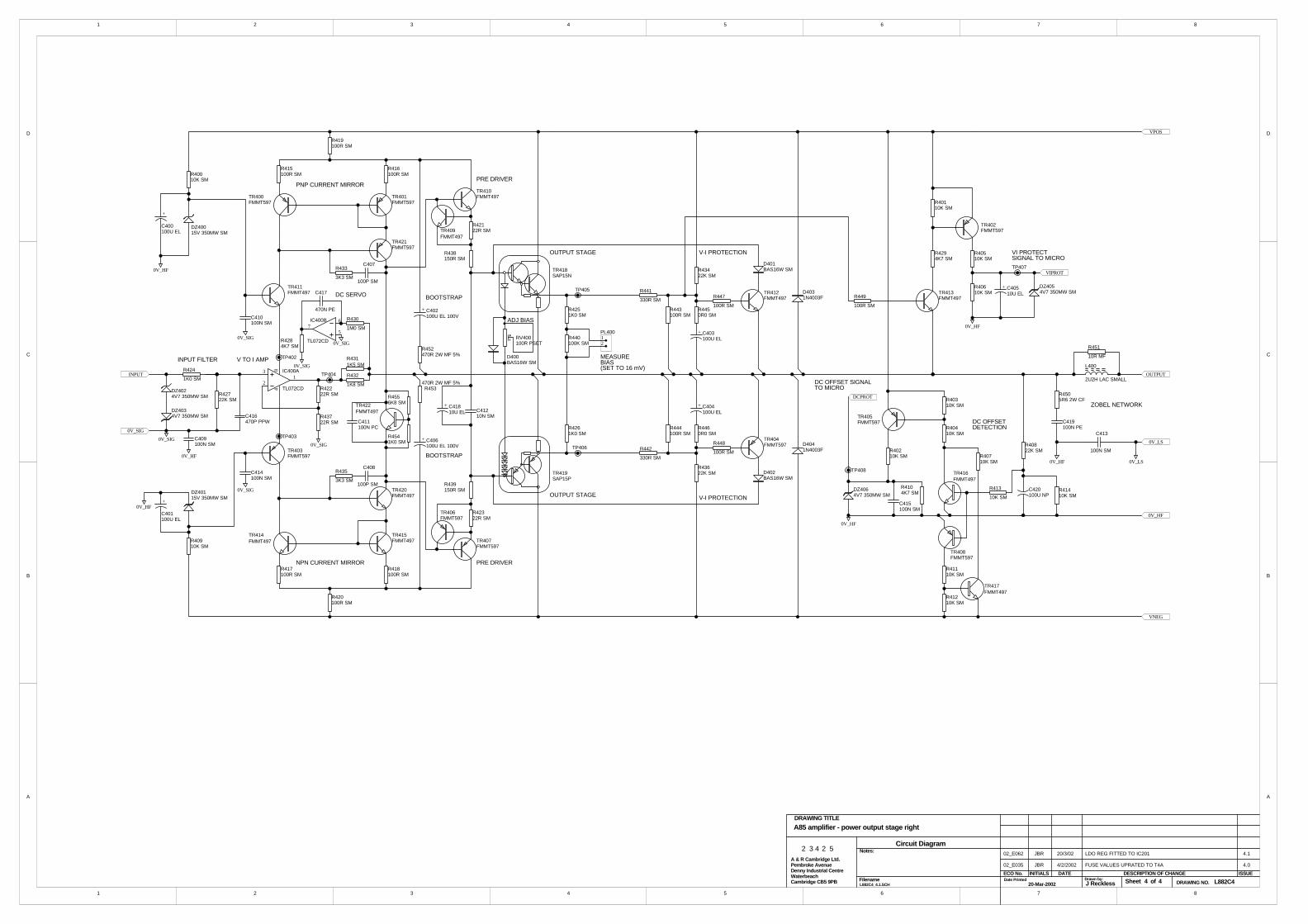
R308, R314 and C320 form a low pass filter from which the DC detection circuits can sense excessive DC at the loudspeaker outputs. If there is any positive DC present, then TR316 will turn on, which turns on TR305 and thus activates the DC protection line to the micro, turning off the loudspeaker relays. If there is any negative DC present, then TR308 will turn on, which turns on TR317 which then turns on TR305 in turn, causing the same effect. R350 and C319 are the Zobel network which is provided to ensure the amplifier ‘sees’ a constant and resistive load at very high frequencies, to aid stability, although the amplifier will be stable without the Zobel fitted. C313 locally couples the ‘high frequency’ and loudspeaker ground returns together at the output to overcome the effects of track inductance back to the star point. C309 couples the ‘high frequency’ and signal grounds together at the input for the same reason. D303 and D304 are ‘flyback’ diodes to protect the output transistors from reverse bias when the amplifier is heavily clipped into an inductive load (such as a loudspeaker voice coil!) Sheet 4 is an identical copy of sheet 3 so I will not describe it separately.
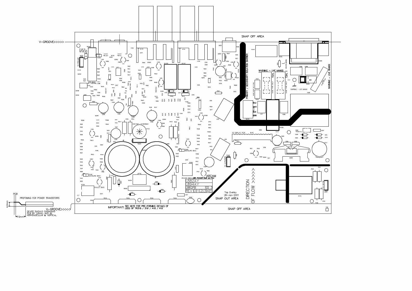
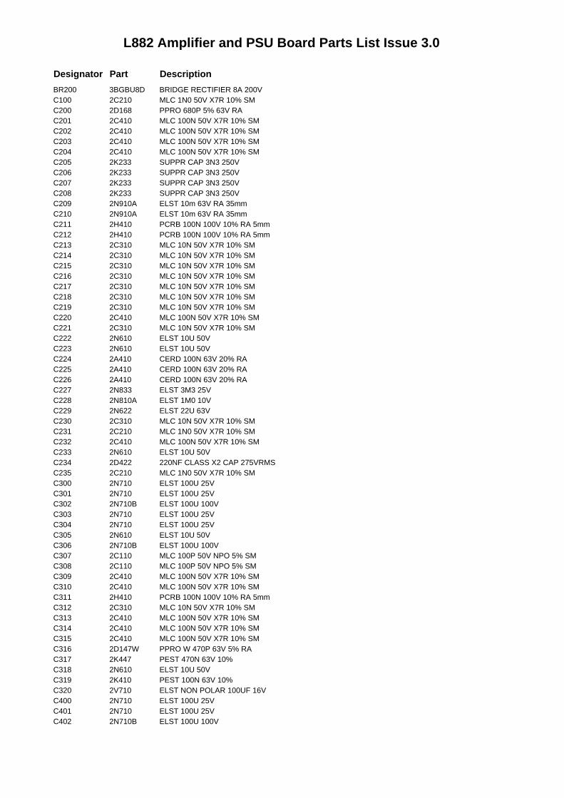
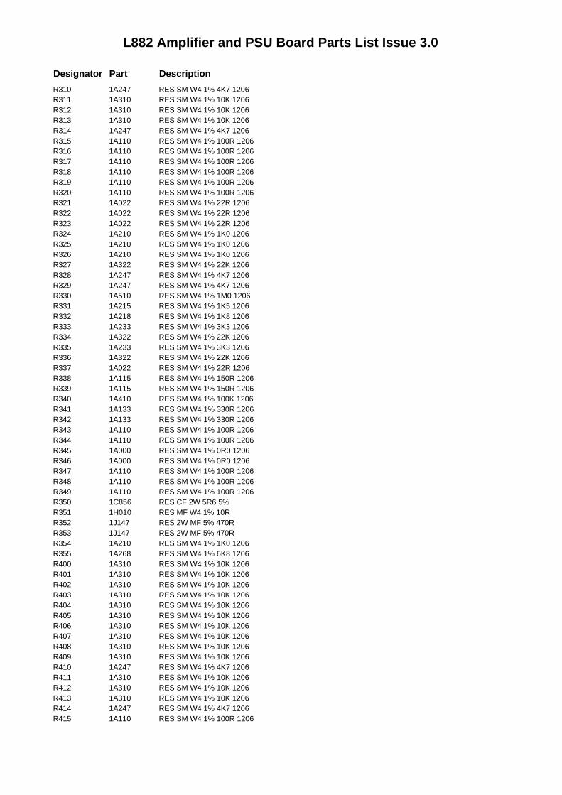
L882 Amplifier and PSU Board Parts List Issue 3.0
Designator Part DescriptionBR200 3BGBU8D BRIDGE RECTIFIER 8A 200VC100 2C210 MLC 1N0 50V X7R 10% SMC200 2D168 PPRO 680P 5% 63V RAC201 2C410 MLC 100N 50V X7R 10% SMC202 2C410 MLC 100N 50V X7R 10% SMC203 2C410 MLC 100N 50V X7R 10% SMC204 2C410 MLC 100N 50V X7R 10% SMC205 2K233 SUPPR CAP 3N3 250VC206 2K233 SUPPR CAP 3N3 250VC207 2K233 SUPPR CAP 3N3 250VC208 2K233 SUPPR CAP 3N3 250VC209 2N910A ELST 10m 63V RA 35mmC210 2N910A ELST 10m 63V RA 35mmC211 2H410 PCRB 100N 100V 10% RA 5mmC212 2H410 PCRB 100N 100V 10% RA 5mmC213 2C310 MLC 10N 50V X7R 10% SMC214 2C310 MLC 10N 50V X7R 10% SMC215 2C310 MLC 10N 50V X7R 10% SMC216 2C310 MLC 10N 50V X7R 10% SMC217 2C310 MLC 10N 50V X7R 10% SMC218 2C310 MLC 10N 50V X7R 10% SMC219 2C310 MLC 10N 50V X7R 10% SMC220 2C410 MLC 100N 50V X7R 10% SMC221 2C310 MLC 10N 50V X7R 10% SMC222 2N610 ELST 10U 50VC223 2N610 ELST 10U 50VC224 2A410 CERD 100N 63V 20% RAC225 2A410 CERD 100N 63V 20% RAC226 2A410 CERD 100N 63V 20% RAC227 2N833 ELST 3M3 25VC228 2N810A ELST 1M0 10VC229 2N622 ELST 22U 63VC230 2C310 MLC 10N 50V X7R 10% SMC231 2C210 MLC 1N0 50V X7R 10% SMC232 2C410 MLC 100N 50V X7R 10% SMC233 2N610 ELST 10U 50VC234 2D422 220NF CLASS X2 CAP 275VRMSC235 2C210 MLC 1N0 50V X7R 10% SMC300 2N710 ELST 100U 25VC301 2N710 ELST 100U 25VC302 2N710B ELST 100U 100VC303 2N710 ELST 100U 25VC304 2N710 ELST 100U 25VC305 2N610 ELST 10U 50VC306 2N710B ELST 100U 100VC307 2C110 MLC 100P 50V NPO 5% SMC308 2C110 MLC 100P 50V NPO 5% SMC309 2C410 MLC 100N 50V X7R 10% SMC310 2C410 MLC 100N 50V X7R 10% SMC311 2H410 PCRB 100N 100V 10% RA 5mmC312 2C310 MLC 10N 50V X7R 10% SMC313 2C410 MLC 100N 50V X7R 10% SMC314 2C410 MLC 100N 50V X7R 10% SMC315 2C410 MLC 100N 50V X7R 10% SMC316 2D147W PPRO W 470P 63V 5% RAC317 2K447 PEST 470N 63V 10%C318 2N610 ELST 10U 50VC319 2K410 PEST 100N 63V 10%C320 2V710 ELST NON POLAR 100UF 16VC400 2N710 ELST 100U 25VC401 2N710 ELST 100U 25VC402 2N710B ELST 100U 100V
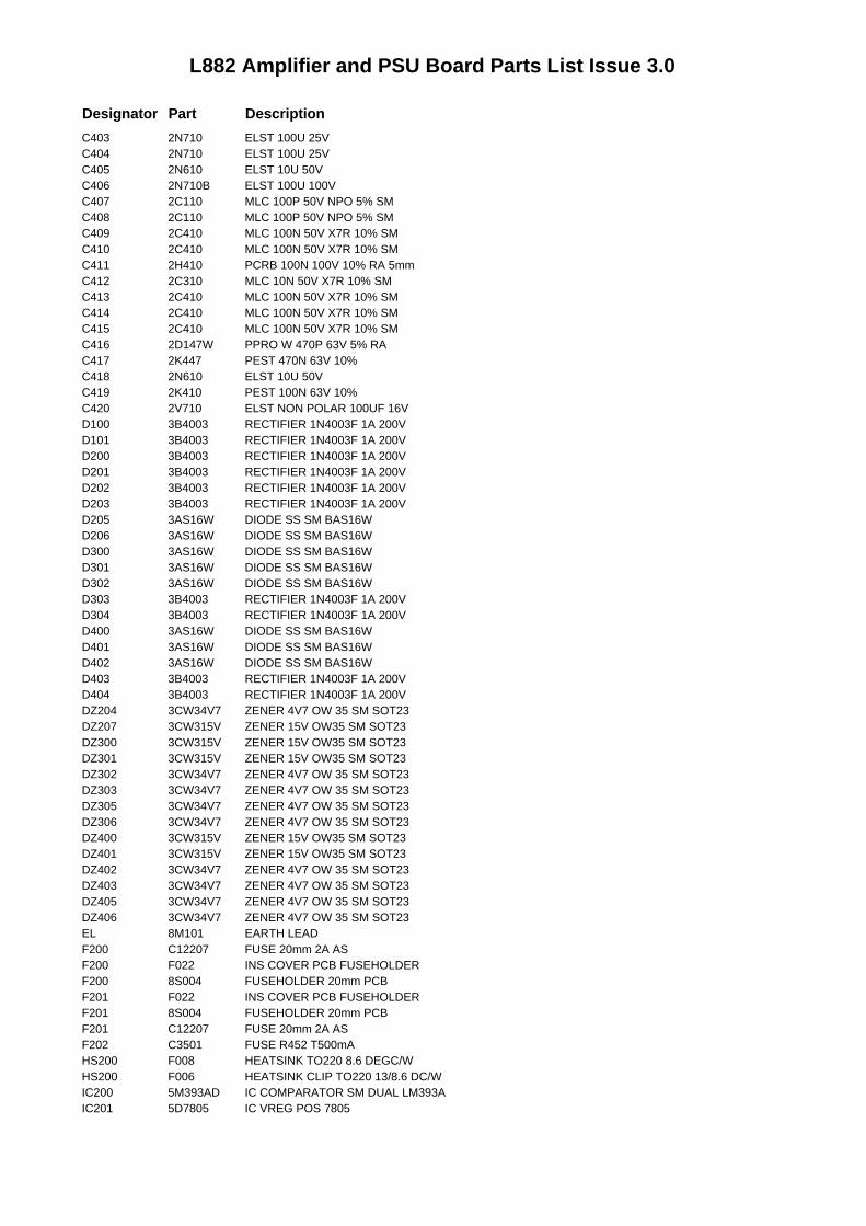
L882 Amplifier and PSU Board Parts List Issue 3.0
Designator Part DescriptionC403 2N710 ELST 100U 25VC404 2N710 ELST 100U 25VC405 2N610 ELST 10U 50VC406 2N710B ELST 100U 100VC407 2C110 MLC 100P 50V NPO 5% SMC408 2C110 MLC 100P 50V NPO 5% SMC409 2C410 MLC 100N 50V X7R 10% SMC410 2C410 MLC 100N 50V X7R 10% SMC411 2H410 PCRB 100N 100V 10% RA 5mmC412 2C310 MLC 10N 50V X7R 10% SMC413 2C410 MLC 100N 50V X7R 10% SMC414 2C410 MLC 100N 50V X7R 10% SMC415 2C410 MLC 100N 50V X7R 10% SMC416 2D147W PPRO W 470P 63V 5% RAC417 2K447 PEST 470N 63V 10%C418 2N610 ELST 10U 50VC419 2K410 PEST 100N 63V 10%C420 2V710 ELST NON POLAR 100UF 16VD100 3B4003 RECTIFIER 1N4003F 1A 200VD101 3B4003 RECTIFIER 1N4003F 1A 200VD200 3B4003 RECTIFIER 1N4003F 1A 200VD201 3B4003 RECTIFIER 1N4003F 1A 200VD202 3B4003 RECTIFIER 1N4003F 1A 200VD203 3B4003 RECTIFIER 1N4003F 1A 200VD205 3AS16W DIODE SS SM BAS16WD206 3AS16W DIODE SS SM BAS16WD300 3AS16W DIODE SS SM BAS16WD301 3AS16W DIODE SS SM BAS16WD302 3AS16W DIODE SS SM BAS16WD303 3B4003 RECTIFIER 1N4003F 1A 200VD304 3B4003 RECTIFIER 1N4003F 1A 200VD400 3AS16W DIODE SS SM BAS16WD401 3AS16W DIODE SS SM BAS16WD402 3AS16W DIODE SS SM BAS16WD403 3B4003 RECTIFIER 1N4003F 1A 200VD404 3B4003 RECTIFIER 1N4003F 1A 200VDZ204 3CW34V7 ZENER 4V7 OW 35 SM SOT23DZ207 3CW315V ZENER 15V OW35 SM SOT23DZ300 3CW315V ZENER 15V OW35 SM SOT23DZ301 3CW315V ZENER 15V OW35 SM SOT23DZ302 3CW34V7 ZENER 4V7 OW 35 SM SOT23DZ303 3CW34V7 ZENER 4V7 OW 35 SM SOT23DZ305 3CW34V7 ZENER 4V7 OW 35 SM SOT23DZ306 3CW34V7 ZENER 4V7 OW 35 SM SOT23DZ400 3CW315V ZENER 15V OW35 SM SOT23DZ401 3CW315V ZENER 15V OW35 SM SOT23DZ402 3CW34V7 ZENER 4V7 OW 35 SM SOT23DZ403 3CW34V7 ZENER 4V7 OW 35 SM SOT23DZ405 3CW34V7 ZENER 4V7 OW 35 SM SOT23DZ406 3CW34V7 ZENER 4V7 OW 35 SM SOT23EL 8M101 EARTH LEADF200 C12207 FUSE 20mm 2A ASF200 F022 INS COVER PCB FUSEHOLDERF200 8S004 FUSEHOLDER 20mm PCBF201 F022 INS COVER PCB FUSEHOLDERF201 8S004 FUSEHOLDER 20mm PCBF201 C12207 FUSE 20mm 2A ASF202 C3501 FUSE R452 T500mAHS200 F008 HEATSINK TO220 8.6 DEGC/WHS200 F006 HEATSINK CLIP TO220 13/8.6 DC/WIC200 5M393AD IC COMPARATOR SM DUAL LM393AIC201 5D7805 IC VREG POS 7805
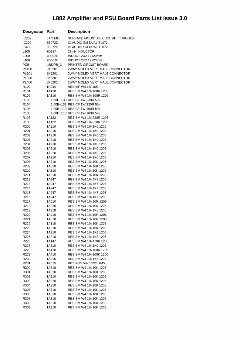
L882 Amplifier and PSU Board Parts List Issue 3.0
Designator Part DescriptionIC202 5J7414D SURFACE MOUNT HEX SCHMITT TRIGGERIC300 5B072D IC AUDIO SM DUAL TL072IC400 5B072D IC AUDIO SM DUAL TL072L200 7D327 27mH INDUCTORL300 7D002C INDUCT 2U2 12x20mmL400 7D002C INDUCT 2U2 12x20mmPCB L882PB_3 PRINTED CIRCUIT BOARDPL100 8K6201 2WAY MOLEX VERT MALE CONNECTORPL101 8K6201 2WAY MOLEX VERT MALE CONNECTORPL300 8K6201 2WAY MOLEX VERT MALE CONNECTORPL400 8K6201 2WAY MOLEX VERT MALE CONNECTORR100 1H010 RES MF W4 1% 10RR101 1A110 RES SM W4 1% 100R 1206R102 1A110 RES SM W4 1% 100R 1206R103 1.00E+133 RES CF 1W 330R 5%R104 1.00E+133 RES CF 1W 330R 5%R105 1.00E+110 RES CF 1W 100R 5%R106 1.00E+110 RES CF 1W 100R 5%R107 1A122 RES SM W4 1% 220R 1206R108 1A122 RES SM W4 1% 220R 1206R200 1A210 RES SM W4 1% 1K0 1206R201 1A210 RES SM W4 1% 1K0 1206R202 1A210 RES SM W4 1% 1K0 1206R203 1A210 RES SM W4 1% 1K0 1206R204 1A210 RES SM W4 1% 1K0 1206R205 1A210 RES SM W4 1% 1K0 1206R206 1A210 RES SM W4 1% 1K0 1206R207 1A210 RES SM W4 1% 1K0 1206R208 1A310 RES SM W4 1% 10K 1206R209 1A310 RES SM W4 1% 10K 1206R210 1A310 RES SM W4 1% 10K 1206R211 1A310 RES SM W4 1% 10K 1206R212 1A247 RES SM W4 1% 4K7 1206R213 1A247 RES SM W4 1% 4K7 1206R214 1A247 RES SM W4 1% 4K7 1206R215 1A247 RES SM W4 1% 4K7 1206R216 1A247 RES SM W4 1% 4K7 1206R217 1A010 RES SM W4 1% 10R 1206R218 1A310 RES SM W4 1% 10K 1206R219 1A218 RES SM W4 1% 1K8 1206R220 1A010 RES SM W4 1% 10R 1206R221 1A010 RES SM W4 1% 10R 1206R222 1A310 RES SM W4 1% 10K 1206R223 1A310 RES SM W4 1% 10K 1206R224 1A218 RES SM W4 1% 1K8 1206R225 1A218 RES SM W4 1% 1K8 1206R226 1A147 RES SM W4 1% 470R 1206R227 1A210 RES SM W4 1% 1K0 1206R228 1A410 RES SM W4 1% 100K 1206R229 1A410 RES SM W4 1% 100K 1206R230 1A215 RES SM W4 1% 1K5 1206R231 1K515 RES W25 5% VR25 1M5R300 1A310 RES SM W4 1% 10K 1206R301 1A310 RES SM W4 1% 10K 1206R302 1A310 RES SM W4 1% 10K 1206R303 1A310 RES SM W4 1% 10K 1206R304 1A310 RES SM W4 1% 10K 1206R305 1A310 RES SM W4 1% 10K 1206R306 1A310 RES SM W4 1% 10K 1206R307 1A310 RES SM W4 1% 10K 1206R308 1A310 RES SM W4 1% 10K 1206R309 1A310 RES SM W4 1% 10K 1206
L882 Amplifier and PSU Board Parts List Issue 3.0
Designator Part DescriptionR310 1A247 RES SM W4 1% 4K7 1206R311 1A310 RES SM W4 1% 10K 1206R312 1A310 RES SM W4 1% 10K 1206R313 1A310 RES SM W4 1% 10K 1206R314 1A247 RES SM W4 1% 4K7 1206R315 1A110 RES SM W4 1% 100R 1206R316 1A110 RES SM W4 1% 100R 1206R317 1A110 RES SM W4 1% 100R 1206R318 1A110 RES SM W4 1% 100R 1206R319 1A110 RES SM W4 1% 100R 1206R320 1A110 RES SM W4 1% 100R 1206R321 1A022 RES SM W4 1% 22R 1206R322 1A022 RES SM W4 1% 22R 1206R323 1A022 RES SM W4 1% 22R 1206R324 1A210 RES SM W4 1% 1K0 1206R325 1A210 RES SM W4 1% 1K0 1206R326 1A210 RES SM W4 1% 1K0 1206R327 1A322 RES SM W4 1% 22K 1206R328 1A247 RES SM W4 1% 4K7 1206R329 1A247 RES SM W4 1% 4K7 1206R330 1A510 RES SM W4 1% 1M0 1206R331 1A215 RES SM W4 1% 1K5 1206R332 1A218 RES SM W4 1% 1K8 1206R333 1A233 RES SM W4 1% 3K3 1206R334 1A322 RES SM W4 1% 22K 1206R335 1A233 RES SM W4 1% 3K3 1206R336 1A322 RES SM W4 1% 22K 1206R337 1A022 RES SM W4 1% 22R 1206R338 1A115 RES SM W4 1% 150R 1206R339 1A115 RES SM W4 1% 150R 1206R340 1A410 RES SM W4 1% 100K 1206R341 1A133 RES SM W4 1% 330R 1206R342 1A133 RES SM W4 1% 330R 1206R343 1A110 RES SM W4 1% 100R 1206R344 1A110 RES SM W4 1% 100R 1206R345 1A000 RES SM W4 1% 0R0 1206R346 1A000 RES SM W4 1% 0R0 1206R347 1A110 RES SM W4 1% 100R 1206R348 1A110 RES SM W4 1% 100R 1206R349 1A110 RES SM W4 1% 100R 1206R350 1C856 RES CF 2W 5R6 5%R351 1H010 RES MF W4 1% 10RR352 1J147 RES 2W MF 5% 470RR353 1J147 RES 2W MF 5% 470RR354 1A210 RES SM W4 1% 1K0 1206R355 1A268 RES SM W4 1% 6K8 1206R400 1A310 RES SM W4 1% 10K 1206R401 1A310 RES SM W4 1% 10K 1206R402 1A310 RES SM W4 1% 10K 1206R403 1A310 RES SM W4 1% 10K 1206R404 1A310 RES SM W4 1% 10K 1206R405 1A310 RES SM W4 1% 10K 1206R406 1A310 RES SM W4 1% 10K 1206R407 1A310 RES SM W4 1% 10K 1206R408 1A310 RES SM W4 1% 10K 1206R409 1A310 RES SM W4 1% 10K 1206R410 1A247 RES SM W4 1% 4K7 1206R411 1A310 RES SM W4 1% 10K 1206R412 1A310 RES SM W4 1% 10K 1206R413 1A310 RES SM W4 1% 10K 1206R414 1A247 RES SM W4 1% 4K7 1206R415 1A110 RES SM W4 1% 100R 1206
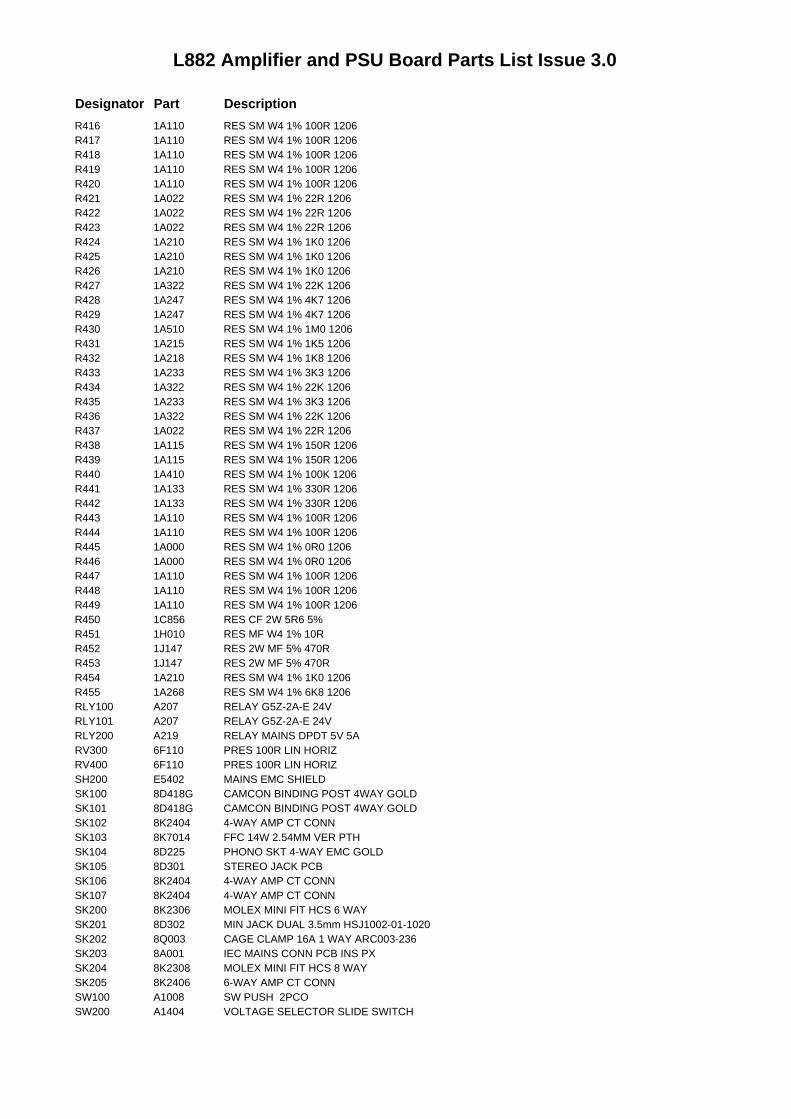
L882 Amplifier and PSU Board Parts List Issue 3.0
Designator Part DescriptionR416 1A110 RES SM W4 1% 100R 1206R417 1A110 RES SM W4 1% 100R 1206R418 1A110 RES SM W4 1% 100R 1206R419 1A110 RES SM W4 1% 100R 1206R420 1A110 RES SM W4 1% 100R 1206R421 1A022 RES SM W4 1% 22R 1206R422 1A022 RES SM W4 1% 22R 1206R423 1A022 RES SM W4 1% 22R 1206R424 1A210 RES SM W4 1% 1K0 1206R425 1A210 RES SM W4 1% 1K0 1206R426 1A210 RES SM W4 1% 1K0 1206R427 1A322 RES SM W4 1% 22K 1206R428 1A247 RES SM W4 1% 4K7 1206R429 1A247 RES SM W4 1% 4K7 1206R430 1A510 RES SM W4 1% 1M0 1206R431 1A215 RES SM W4 1% 1K5 1206R432 1A218 RES SM W4 1% 1K8 1206R433 1A233 RES SM W4 1% 3K3 1206R434 1A322 RES SM W4 1% 22K 1206R435 1A233 RES SM W4 1% 3K3 1206R436 1A322 RES SM W4 1% 22K 1206R437 1A022 RES SM W4 1% 22R 1206R438 1A115 RES SM W4 1% 150R 1206R439 1A115 RES SM W4 1% 150R 1206R440 1A410 RES SM W4 1% 100K 1206R441 1A133 RES SM W4 1% 330R 1206R442 1A133 RES SM W4 1% 330R 1206R443 1A110 RES SM W4 1% 100R 1206R444 1A110 RES SM W4 1% 100R 1206R445 1A000 RES SM W4 1% 0R0 1206R446 1A000 RES SM W4 1% 0R0 1206R447 1A110 RES SM W4 1% 100R 1206R448 1A110 RES SM W4 1% 100R 1206R449 1A110 RES SM W4 1% 100R 1206R450 1C856 RES CF 2W 5R6 5%R451 1H010 RES MF W4 1% 10RR452 1J147 RES 2W MF 5% 470RR453 1J147 RES 2W MF 5% 470RR454 1A210 RES SM W4 1% 1K0 1206R455 1A268 RES SM W4 1% 6K8 1206RLY100 A207 RELAY G5Z-2A-E 24VRLY101 A207 RELAY G5Z-2A-E 24VRLY200 A219 RELAY MAINS DPDT 5V 5ARV300 6F110 PRES 100R LIN HORIZRV400 6F110 PRES 100R LIN HORIZSH200 E5402 MAINS EMC SHIELDSK100 8D418G CAMCON BINDING POST 4WAY GOLDSK101 8D418G CAMCON BINDING POST 4WAY GOLDSK102 8K2404 4-WAY AMP CT CONNSK103 8K7014 FFC 14W 2.54MM VER PTHSK104 8D225 PHONO SKT 4-WAY EMC GOLDSK105 8D301 STEREO JACK PCBSK106 8K2404 4-WAY AMP CT CONNSK107 8K2404 4-WAY AMP CT CONNSK200 8K2306 MOLEX MINI FIT HCS 6 WAYSK201 8D302 MIN JACK DUAL 3.5mm HSJ1002-01-1020SK202 8Q003 CAGE CLAMP 16A 1 WAY ARC003-236SK203 8A001 IEC MAINS CONN PCB INS PXSK204 8K2308 MOLEX MINI FIT HCS 8 WAYSK205 8K2406 6-WAY AMP CT CONNSW100 A1008 SW PUSH 2PCOSW200 A1404 VOLTAGE SELECTOR SLIDE SWITCH
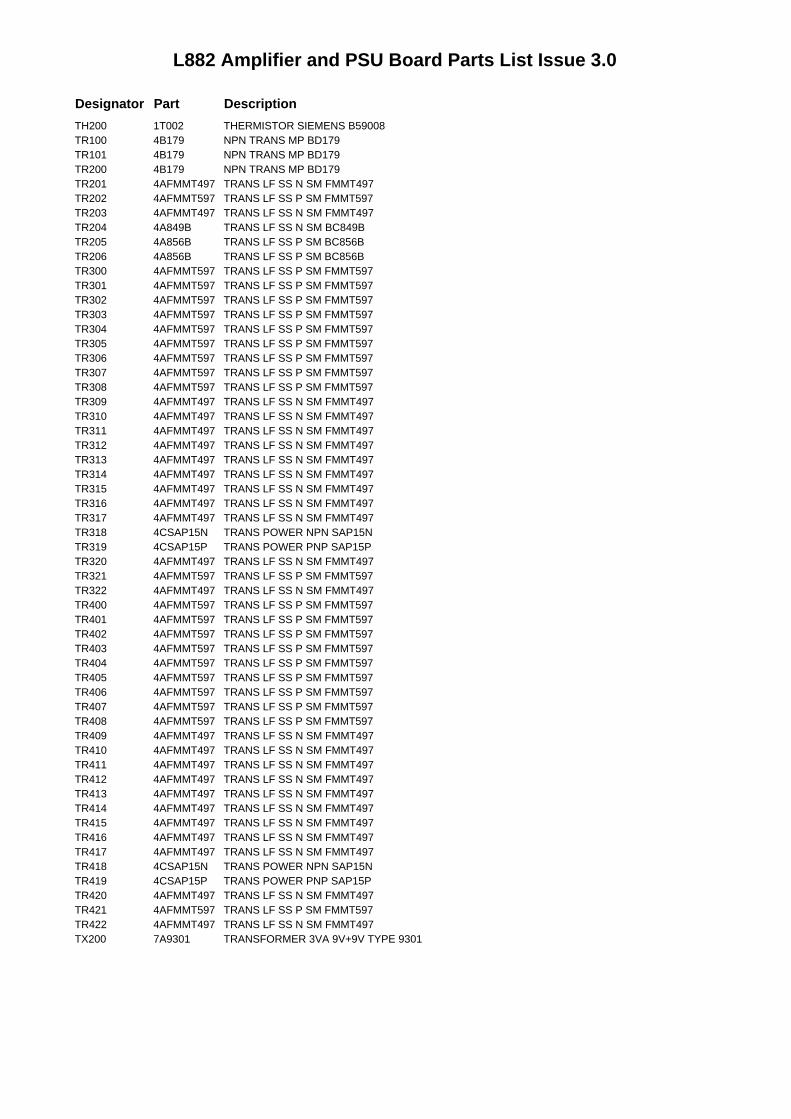
L882 Amplifier and PSU Board Parts List Issue 3.0
Designator Part DescriptionTH200 1T002 THERMISTOR SIEMENS B59008TR100 4B179 NPN TRANS MP BD179TR101 4B179 NPN TRANS MP BD179TR200 4B179 NPN TRANS MP BD179TR201 4AFMMT497 TRANS LF SS N SM FMMT497TR202 4AFMMT597 TRANS LF SS P SM FMMT597TR203 4AFMMT497 TRANS LF SS N SM FMMT497TR204 4A849B TRANS LF SS N SM BC849BTR205 4A856B TRANS LF SS P SM BC856BTR206 4A856B TRANS LF SS P SM BC856BTR300 4AFMMT597 TRANS LF SS P SM FMMT597TR301 4AFMMT597 TRANS LF SS P SM FMMT597TR302 4AFMMT597 TRANS LF SS P SM FMMT597TR303 4AFMMT597 TRANS LF SS P SM FMMT597TR304 4AFMMT597 TRANS LF SS P SM FMMT597TR305 4AFMMT597 TRANS LF SS P SM FMMT597TR306 4AFMMT597 TRANS LF SS P SM FMMT597TR307 4AFMMT597 TRANS LF SS P SM FMMT597TR308 4AFMMT597 TRANS LF SS P SM FMMT597TR309 4AFMMT497 TRANS LF SS N SM FMMT497TR310 4AFMMT497 TRANS LF SS N SM FMMT497TR311 4AFMMT497 TRANS LF SS N SM FMMT497TR312 4AFMMT497 TRANS LF SS N SM FMMT497TR313 4AFMMT497 TRANS LF SS N SM FMMT497TR314 4AFMMT497 TRANS LF SS N SM FMMT497TR315 4AFMMT497 TRANS LF SS N SM FMMT497TR316 4AFMMT497 TRANS LF SS N SM FMMT497TR317 4AFMMT497 TRANS LF SS N SM FMMT497TR318 4CSAP15N TRANS POWER NPN SAP15NTR319 4CSAP15P TRANS POWER PNP SAP15PTR320 4AFMMT497 TRANS LF SS N SM FMMT497TR321 4AFMMT597 TRANS LF SS P SM FMMT597TR322 4AFMMT497 TRANS LF SS N SM FMMT497TR400 4AFMMT597 TRANS LF SS P SM FMMT597TR401 4AFMMT597 TRANS LF SS P SM FMMT597TR402 4AFMMT597 TRANS LF SS P SM FMMT597TR403 4AFMMT597 TRANS LF SS P SM FMMT597TR404 4AFMMT597 TRANS LF SS P SM FMMT597TR405 4AFMMT597 TRANS LF SS P SM FMMT597TR406 4AFMMT597 TRANS LF SS P SM FMMT597TR407 4AFMMT597 TRANS LF SS P SM FMMT597TR408 4AFMMT597 TRANS LF SS P SM FMMT597TR409 4AFMMT497 TRANS LF SS N SM FMMT497TR410 4AFMMT497 TRANS LF SS N SM FMMT497TR411 4AFMMT497 TRANS LF SS N SM FMMT497TR412 4AFMMT497 TRANS LF SS N SM FMMT497TR413 4AFMMT497 TRANS LF SS N SM FMMT497TR414 4AFMMT497 TRANS LF SS N SM FMMT497TR415 4AFMMT497 TRANS LF SS N SM FMMT497TR416 4AFMMT497 TRANS LF SS N SM FMMT497TR417 4AFMMT497 TRANS LF SS N SM FMMT497TR418 4CSAP15N TRANS POWER NPN SAP15NTR419 4CSAP15P TRANS POWER PNP SAP15PTR420 4AFMMT497 TRANS LF SS N SM FMMT497TR421 4AFMMT597 TRANS LF SS P SM FMMT597TR422 4AFMMT497 TRANS LF SS N SM FMMT497TX200 7A9301 TRANSFORMER 3VA 9V+9V TYPE 9301
1 2 3 4 5 6 7 8
A
B
C
D
87654321
D
C
B
A
ISSUE
DRAWING NO.
23425
DRAWING TITLE
Drawn by:DATE
FilenameECO No. DESCRIPTION OF CHANGE
L882C1_4.1.PRJ
A & R Cambridge Ltd.Pembroke AvenueDenny Industrial CentreWaterbeachCambridge CB5 9PB
A85 amplifier and PSU - top sheet
Circuit Diagram
L882C1J Reckless20-Mar-2002
INITIALSDate Printed 1 4Sheet of
Notes:
Top+
Top-
SK100A
CAMCON_G
Bot+
Bot-
SK100B
CAMCON_G
Top+
Top-
SK101A
CAMCON_G
Bot+
Bot-
SK101B
CAMCON_G
D1001N4003F
D1011N4003F
1 2
34
5 6
78SP100
STAR_8
EMC
1
N
FSK104A
PHONO4G
N
F
SK104B
PHONO4G
0V_SIG0V_SIG
0V_SIG
1 2 3
SW100A2PCO
4 5 6
SW100B2PCO
C1001N0 SM
1234
SK102
AMPCT4
STANDBYSPKR1 ONSPKR2 ONTHERMPROTVIPROTDCPROTAC PRESENT
L SIG
R SIG
SPKR1 ON
SPKR2 ON
THERMPROTVIPROTAC PRESENTDCPROT
LS L
LS R
L SIG0V_SIG0V_LS_L0V_HF_L+49V-49V +5V_D
+49V-49V
0V_D0V_PSU
R SIG0V_SIG0V_LS_R0V_HF_R+49V-49V
0V_TRIG
LS L
0V_LS_L
0V_LS_R
LS R
+49V
0V_D
VIPROT_LDCPROT_L
DCPROT_LVIPROT_RDCPROT_R
DCPROT_R
VIPROT_LVIPROT_R
STANDBY
+49V
+5V_D
0V_D
0V_PSU
0V_LS_R
0V_HF_R
0V_LS_L0V_HF_L
0V_D
0V_TRIG
0V_SIG
R103
330R 1W CFR104
330R 1W CF
R105100R 1W CF
R106100R 1W CF
1234
SK106
AMPCT4
231
45
67
SK105
HPSKT
1234
SK107
AMPCT4
LS L
LS R
0V_LS_L
REMOTE
REMOTE
FROM PREAMP
INTEGRATED / PRE-POWERMODE SELECT SWITCH
TRIGGER
TRIGGER
TP102
TP101
TP100
TP103TP104
TP105TP106
TP107TP108
TP109TP110
TP117
TP111 TP113 TP115
TP112 TP114 TP116
0V_D +5V(D)VPOSVNEG
0V_PSUPWRON
THPROT_uCVIPROT_LVIPROT_R VIPROT_uC
AC_PRES0V_TRIGDCPROT_LDCPROT_R
DCPROT_uCRC5 INTRG IN
L882C2L882C2_4.1.SCH
INPUT0V_SIG
VIPROTDCPROTOUTPUT0V_LS
0V_HFVPOSVNEG
L882C3L882C3_4.1.SCH
INPUT0V_SIG
VIPROTDCPROTOUTPUT0V_LS
0V_HFVPOSVNEG
L882C4L882C4_4.1.SCH
RLY100A
RLY G5Z-2A-E
RLY100B
RLY G5Z-2A-E
RLY100CRLY G5Z-2A-E
RLY101A
RLY G5Z-2A-E
RLY101B
RLY G5Z-2A-E
RLY101CRLY G5Z-2A-E
TR100BD179
TR101BD179
R101
100R SM
R102
100R SM
R107220R SM
R108220R SM
PCB
PCB
L882PB_4
TP118
TP119
TP120
TP121
1234567891011121314
SK103
FFC 14W 2.54MM VER8K7014
EARTH LEAD8M101
EL
EARTH LEAD
12
PL100
12
PL101
R100
10R MF
02_E035 JBR 4/2/2002 FUSE VALUES UPRATED TO T4A 4.0
02_E062 JBR 20/3/02 LDO REG FITTED TO IC201 4.1
1 2 3 4 5 6 7 8
A
B
C
D
87654321
D
C
B
A
ISSUE
DRAWING NO.
23425
DRAWING TITLE
Drawn by:DATE
FilenameECO No. DESCRIPTION OF CHANGE
L882C2_4.1.SCH
A & R Cambridge Ltd.Pembroke AvenueDenny Industrial CentreWaterbeachCambridge CB5 9PB
A85 amplifier - power supply and microcontroller interface
Circuit Diagram
L882C2J Reckless20-Mar-2002
INITIALSDate Printed 2 4Sheet of
Notes:
LN E
N E L
SK203IEC3 NO RIVETS
BC200TOOLING4.1
Gre
en1
SK202CAGECLAMP1
C2053N3 MAINS
C2063N3 MAINS
Far from PCB
SK201B
JACK3.5X2
Near to PCB
SK201A
JACK3.5X2
SW200BVOL SEL SLIDE
SW200AVOL SEL SLIDE
C208
3N3 MAINS
C207
3N3 MAINS
VinI
GN
DG
Vout O
IC201L4940V5
D2031N4003F
D2011N4003F
D2021N4003F
D2001N4003F
C225100N CD
C226100N CD
VR201VDR 115V
VR200VDR 115V
+1
~ 2
-4
~3
BR200BRGBU8D
LIVENEUTRAL
EARTH
EMC Shield
SH200EMCMAINS
NEUTRAL
LIVE
LIVE
NEUTRAL
0V_D
+5V(D)
0V_D
0V_PSU
VPOS
VNEG
0V_PSU
+49V
+5V_D
0V_D
PWRON
-49V
+5V_D
TH200PTH90DEG
+5V_D
0V_D
THPROT_uC
VIPROT_L
VIPROT_R
+5V_D
0V_D
VIPROT_uC
0V_D
9VRMS
+5V_D
0V_D
9VRMS
+ C22922U EL
AC_PRES
+
C2273300u 25V
+ C2281000u 10V
2
3
4
6
7
8
1 5
SK204
MOLEXPWR8
1
2
3
4
5
6SK200
MOLEXPWR6
D206BAS16W SM
TR204BC849B
R211
10K SM
R220
10R SM
R2001K0 SM TR202
FMMT597
D205BAS16W SM C213
10N SM
TR203FMMT497
DZ20715V 350MW SM
+ C22310U EL
+ C22210U EL
R21010K SM
+49V
0V_TRIG
0V_TRIG
1 2
IC202A
74HC14D
3 4
IC202B
74HC14D
1011
IC202E
74HC14D
1213
IC202F
74HC14D
C21410N SM
C21510N SM
R213
4K7 SM
R214
4K7 SM
TR205BC856B
R2061K0 SM C218
10N SM
C203100N SM
DCPROT_L
DCPROT_R
+5V_D
0V_D
DCPROT_uC
0V_D
5 6
IC202C
74HC14D
89
IC202D
74HC14D
C21610N SM
C21710N SM
R215
4K7 SM
R216
4K7 SM
TR206BC856B
R2071K0 SM C220
100N SM
C204100N SM
14
7
IC202G74HC14D
C201100N SM
C202100N SM
R2051K0 SM
R221
10R SM
C224100N CD
R2191K8 SM
R212
4K7 SM
TR201FMMT497
TRIGGER OUTPUTAPPROX 13.5VDC60mA MAX CURRENT
R201
1K0 SM
R202
1K0 SM
R203
1K0 SM
R204
1K0 SM
C21910N SM
C22110N SM
MAINS WIRING AND AUXILIARY SUPPLY
POWER AMP SUPPLY
MICROPROCESSOR SIGNALS INTERFACE
HS
HS200TO220HS08REG
123456
SK205
AMPCT6
RLY200A
DPDT5V
RLY200B
DPDT5V
RLY200CDPDT5V
115V
115V6
4
2
1 0V
5
8
9V
0V
9V
37
0V
TX200
TX 3VA 9301
TR200BD179
R21710R SM
R21810K SM
STANDBY RELAY CONTROL
R2271K0 SM
DZ2044V7 350MW SM
R228
100K SM
L20027mH C200
680P PP
3
21
IC200A
LM393A SM
R22310K SM
R229100K SM
R20910K SM
R2241K8 SM
R2301K5 SM
5
67
IC200B
LM393A SM
84
IC200CLM393A SM
R2251K8 SM
C2311N0 SM
R20810K SM
C232100N SM
0V_TRIG
+5V_D
RC5 IN
CARRIER FILTER AND DEMODULATOR
C23010N SM
MODULATED RC5REMOTE CONTROL INPUT
+ C23310U EL
R222
10K SM
TRG IN
TP206
TP200
TP207
TP203
TP201
TP202
TP210
TP204
TP205
TP208
TP209
TP211
TP212
+ C20910,000u 63V
+ C21010,000u 63V
R226
470R SM
C211100N PC
C212100N PC
CHASS
SK101CCAMCON_G
C235
1N0 SM
C234
220N X2 CLASS
R231
1M5 VR25
NF
NF
F202
T750mA SM
02_E035 JBR 4/2/2002 FUSE VALUES UPRATED TO T4A 4.0
F200
T4A
F201
T4A
02_E062 JBR 20/3/02 LDO REG FITTED TO IC201 4.1
1 2 3 4 5 6 7 8
A
B
C
D
87654321
D
C
B
A
ISSUE
DRAWING NO.
23425
DRAWING TITLE
Drawn by:DATE
FilenameECO No. DESCRIPTION OF CHANGE
L882C3_4.1.SCH
A & R Cambridge Ltd.Pembroke AvenueDenny Industrial CentreWaterbeachCambridge CB5 9PB
A85 amplifier - power output stage left
Circuit Diagram
L882C3J Reckless20-Mar-2002
INITIALSDate Printed 3 4Sheet of
Notes:
R324
1K0 SM
TR300FMMT597
TR301FMMT597
R315100R SM
R316100R SM
R319100R SM
TR314FMMT497
TR315FMMT497
R317100R SM
R318100R SM
R320100R SM
R32222R SM
0V_SIG
C317
470N PE
0V_SIG
0V_SIG
INPUT
0V_SIG
R3505R6 2W CF
C319100N PE
0V_HF 0V_LS
C313
100N SM
R341
330R SM
R342
330R SM
R343100R SM
R344100R SM
R3450R0 SM
R3460R0 SM
R33422K SM
R33622K SM
D301BAS16W SM
D302BAS16W SM
TR312FMMT497
TR304FMMT597
TR313FMMT497
TR302FMMT597
DZ3054V7 350MW SM
0V_HF
VIPROT
C320100U NP
TR305FMMT597
DZ3064V7 350MW SM
0V_HF
DCPROT
OUTPUT
0V_LS
0V_HF
VPOS
VNEG
0V_HF
0V_HF
DZ30015V 350MW SM
DZ30115V 350MW SM
C309100N SM
C310100N SM
C314100N SM
0V_SIG
0V_SIG
D3041N4003F
D3031N4003F
R30210K SM
R32722K SM
RV300100R PSET
C31210N SM
12
PL300
BIAS
R3251K0 SM
R3261K0 SM
ADJ BIAS
D300BAS16W SM
R30010K SM
R30910K SM
R30510K SM
R30610K SM
+ C30510U EL
MEASURE
TR318SAP15N
TR319SAP15P
R30110K SM
C315100N SM
R347
100R SM
R349
100R SM
R348
100R SM
R340100K SM
DZ3024V7 350MW SM
DZ3034V7 350MW SM
3
21
84
IC300A
TL072CD
5
67IC300B
TL072CDR3284K7 SM
0V_HF
0V_SIG
TR311FMMT497
TR303FMMT597
TR310FMMT497
TR307FMMT597
C307
100P SM
C308
100P SM
INPUT FILTER V TO I AMP
DC SERVO
PNP CURRENT MIRROR
NPN CURRENT MIRROR
PRE DRIVER
PRE DRIVER
OUTPUT STAGE
OUTPUT STAGE
V-I PROTECTION
V-I PROTECTION
VI PROTECTSIGNAL TO MICRO
DC OFFSETDETECTION
DC OFFSET SIGNALTO MICRO
ZOBEL NETWORK
TR316FMMT497
TR308FMMT597
TR317FMMT497
R31110K SM
R31210K SM
R313
10K SM
R30310K SM
R30410K SM
R30710K SM
R3104K7 SM
R3294K7 SM
+
C300100U EL
+
C301100U EL
R338150R SM
R339150R SM
R30822K SM
R31410K SM
TR309FMMT497
TR306FMMT597
R32322R SM
R32122R SM
TP302
TP303
TP304
TP307
TP308
TP305
TP306
R33722R SM
R3311K5 SM
R332
1K8 SM
R330
1M0 SM
R333
3K3 SM
R335
3K3 SM
L300
2U2H LAC SMALL
R351
10R MF
C316470P PPW
C311100N PC
+ C31810U EL
TR321FMMT597
TR320FMMT497
+ C302100U EL 100V
+ C306100U EL 100V
R352470R 2W MF 5%
R353470R 2W MF 5%
BOOTSTRAP
BOOTSTRAP
(SET TO 16mV)
+ C303100U EL
+ C304100U EL
TR322FMMT497
R3541K0 SM
R3556K8 SM
02_E035 JBR 4/2/2002 FUSE VALUES UPRATED TO T4A 4.0
02_E062 JBR 20/3/02 LDO REG FITTED TO IC201 4.1
1 2 3 4 5 6 7 8
A
B
C
D
87654321
D
C
B
A
ISSUE
DRAWING NO.
23425
DRAWING TITLE
Drawn by:DATE
FilenameECO No. DESCRIPTION OF CHANGE
L882C4_4.1.SCH
A & R Cambridge Ltd.Pembroke AvenueDenny Industrial CentreWaterbeachCambridge CB5 9PB
A85 amplifier - power output stage right
Circuit Diagram
L882C4J Reckless20-Mar-2002
INITIALSDate Printed 4 4Sheet of
Notes:
R424
1K0 SM
TR400FMMT597
TR401FMMT597
R415100R SM
R416100R SM
R419100R SM
TR414FMMT497
TR415FMMT497
R417100R SM
R418100R SM
R420100R SM
R42222R SM
0V_SIG
R430
1M0 SM
R4311K5 SM
R432
1K8 SM
C417
470N PE
0V_SIG
0V_SIG
INPUT
0V_SIG
R4505R6 2W CF
C419100N PE
0V_HF 0V_LS
C413
100N SM
R441
330R SM
R442
330R SM
R443100R SM
R444100R SM
R4450R0 SM
R4460R0 SM
R43422K SM
R43622K SM
D401BAS16W SM
D402BAS16W SM
TR412FMMT497
TR404FMMT597
TR413FMMT497
TR402FMMT597
DZ4054V7 350MW SM
0V_HF
VIPROT
C420100U NP
TR405FMMT597
DZ4064V7 350MW SM
0V_HF
DCPROT
OUTPUT
0V_LS
0V_HF
VPOS
VNEG
0V_HF
0V_HF
DZ40015V 350MW SM
DZ40115V 350MW SM
C409100N SM
C410100N SM
C414100N SM
0V_SIG
0V_SIG
D4041N4003F
D4031N4003F
R40210K SM
R42722K SM
RV400100R PSET
C41210N SM
12
PL400
BIAS
R4251K0 SM
R4261K0 SM
ADJ BIAS
D400BAS16W SM
R40010K SM
R40910K SM
R40510K SM
R40610K SM
+ C40510U EL
MEASURE
TR418SAP15N
TR419SAP15P
R40110K SM
C415100N SM
R447
100R SM
R449
100R SM
R448
100R SM
R440100K SM
DZ4024V7 350MW SM
DZ4034V7 350MW SM
3
21
84
IC400A
TL072CD
5
67IC400B
TL072CDR4284K7 SM
0V_HF
0V_SIG
TR411FMMT497
TR403FMMT597
TR410FMMT497
TR407FMMT597
C407
100P SM
C408
100P SM
INPUT FILTER V TO I AMP
DC SERVO
PNP CURRENT MIRROR
NPN CURRENT MIRROR
PRE DRIVER
PRE DRIVER
OUTPUT STAGE
OUTPUT STAGE
V-I PROTECTION
V-I PROTECTION
VI PROTECTSIGNAL TO MICRO
DC OFFSETDETECTION
DC OFFSET SIGNALTO MICRO
ZOBEL NETWORK
TR416FMMT497
TR408FMMT597
TR417FMMT497
R41110K SM
R41210K SM
R413
10K SM
R40310K SM
R40410K SM
R40710K SM
R4104K7 SM
R4294K7 SM
+
C400100U EL
+
C401100U EL
R438150R SM
R439150R SM
R40822K SM
R41410K SM
TR409FMMT497
TR406FMMT597
R42322R SM
R42122R SM
(SET TO 16 mV)
TP402
TP403
TP404
TP405
TP406
TP407
TP408
R43722R SM
R433
3K3 SM
R435
3K3 SM
R451
10R MF
C416470P PPW C411
100N PC
+ C41810U EL
TR421FMMT597
TR420FMMT497
+ C402100U EL 100V
+ C406100U EL 100V
R452470R 2W MF 5%
R453470R 2W MF 5%
BOOTSTRAP
BOOTSTRAP
+ C403100U EL
+ C404100U EL
L400
2U2H LAC SMALL
TR422FMMT497
R4541K0 SM
R4556K8 SM
02_E035 JBR 4/2/2002 FUSE VALUES UPRATED TO T4A 4.0
02_E062 JBR 20/3/02 LDO REG FITTED TO IC201 4.1
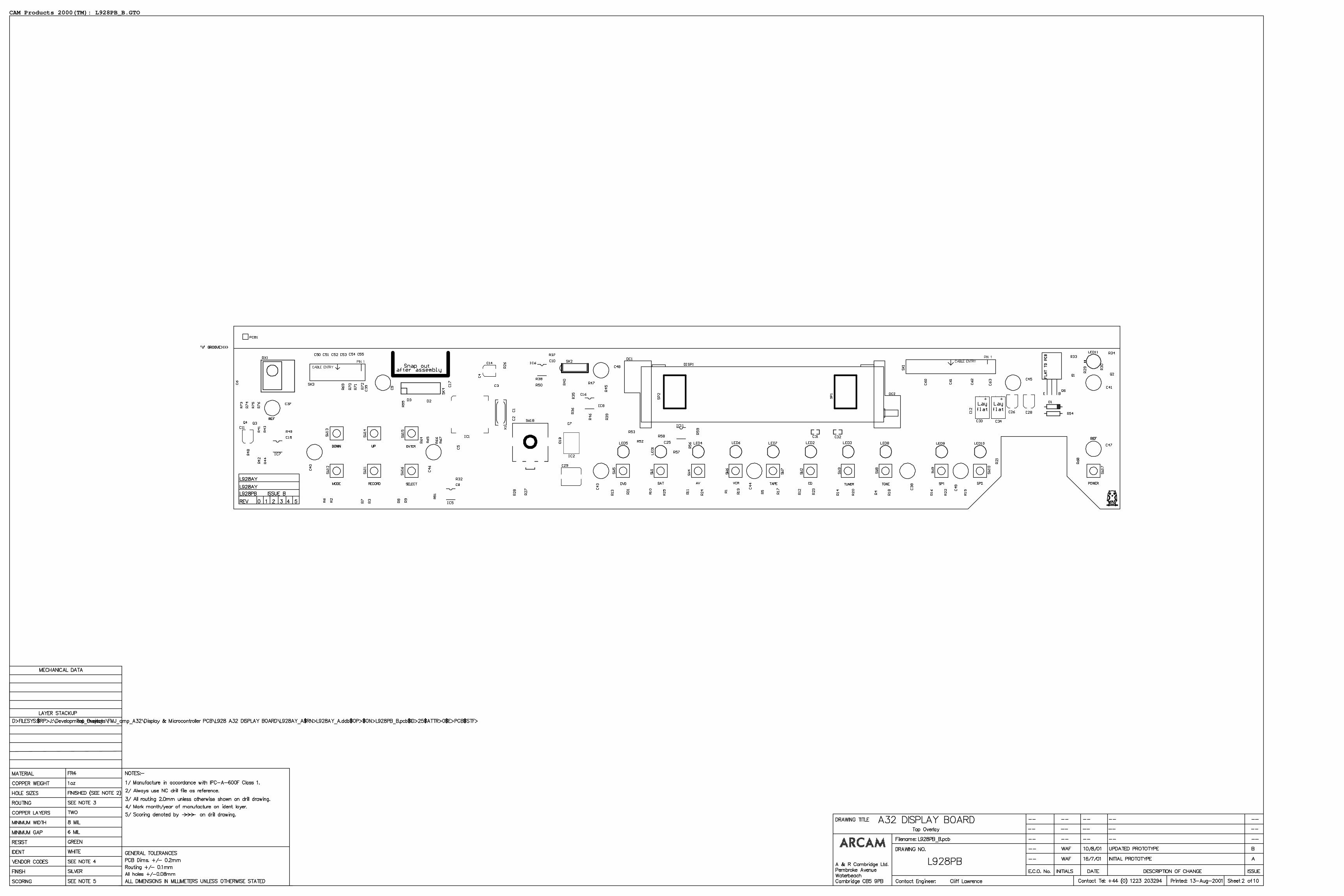
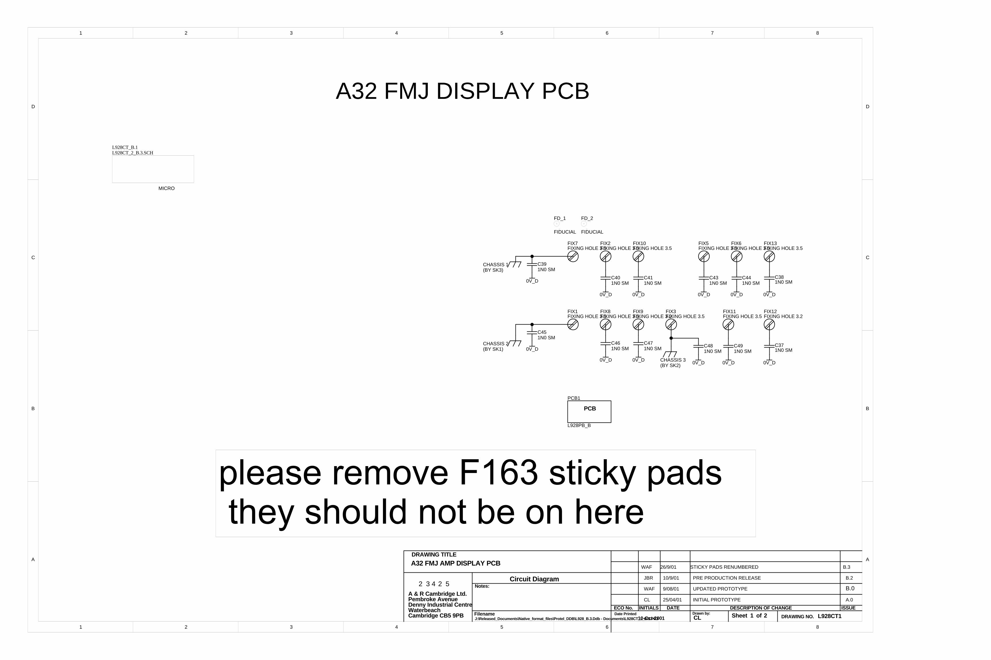
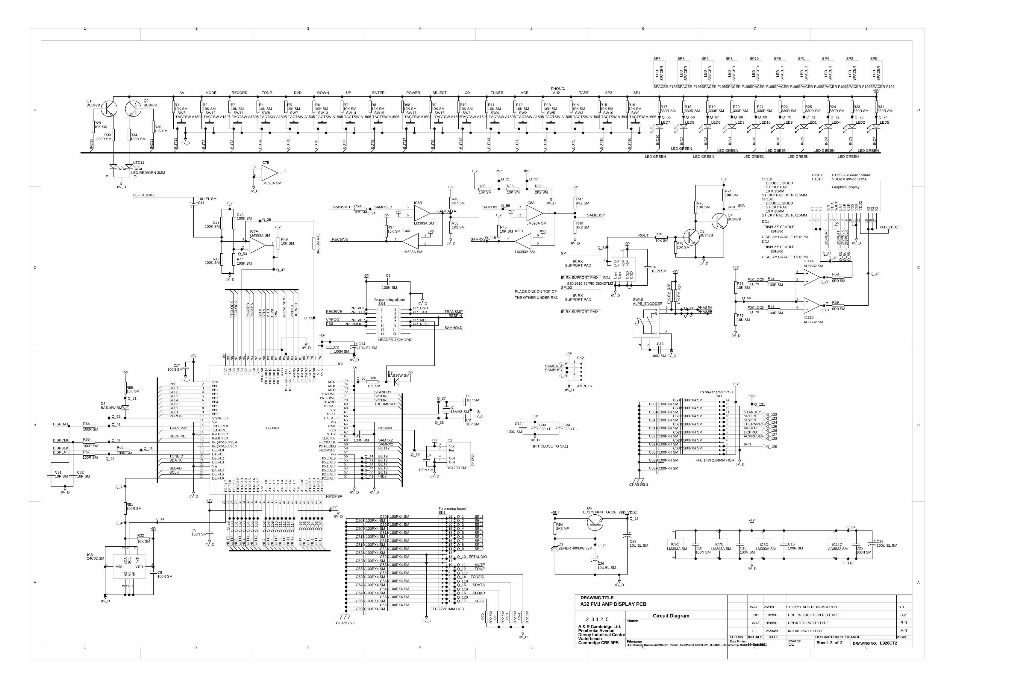
Display Board L928
Contents
! Component overlay
! Parts list
! Circuit diagrams
CAM Products 2000(TM): L928PB_B.GTO
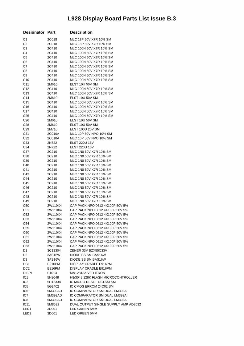
L928 Display Board Parts List Issue B.3
Designator Part DescriptionC1 2C018 MLC 18P 50V X7R 10% SMC2 2C018 MLC 18P 50V X7R 10% SMC3 2C410 MLC 100N 50V X7R 10% SMC4 2C410 MLC 100N 50V X7R 10% SMC5 2C410 MLC 100N 50V X7R 10% SMC6 2C410 MLC 100N 50V X7R 10% SMC7 2C410 MLC 100N 50V X7R 10% SMC8 2C410 MLC 100N 50V X7R 10% SMC9 2C410 MLC 100N 50V X7R 10% SMC10 2C410 MLC 100N 50V X7R 10% SMC11 2M610 ELST 10U 50V SMC12 2C410 MLC 100N 50V X7R 10% SMC13 2C410 MLC 100N 50V X7R 10% SMC14 2M610 ELST 10U 50V SMC15 2C410 MLC 100N 50V X7R 10% SMC16 2C410 MLC 100N 50V X7R 10% SMC17 2C410 MLC 100N 50V X7R 10% SMC25 2C410 MLC 100N 50V X7R 10% SMC26 2M610 ELST 10U 50V SMC28 2M610 ELST 10U 50V SMC29 2M710 ELST 100U 25V SMC31 2C010A MLC 10P 50V NPO 10% SMC32 2C010A MLC 10P 50V NPO 10% SMC33 2N722 ELST 220U 16VC34 2N722 ELST 220U 16VC37 2C210 MLC 1N0 50V X7R 10% SMC38 2C210 MLC 1N0 50V X7R 10% SMC39 2C210 MLC 1N0 50V X7R 10% SMC40 2C210 MLC 1N0 50V X7R 10% SMC41 2C210 MLC 1N0 50V X7R 10% SMC43 2C210 MLC 1N0 50V X7R 10% SMC44 2C210 MLC 1N0 50V X7R 10% SMC45 2C210 MLC 1N0 50V X7R 10% SMC46 2C210 MLC 1N0 50V X7R 10% SMC47 2C210 MLC 1N0 50V X7R 10% SMC48 2C210 MLC 1N0 50V X7R 10% SMC49 2C210 MLC 1N0 50V X7R 10% SMC50 2W110X4 CAP PACK NPO 0612 4X100P 50V 5%C51 2W110X4 CAP PACK NPO 0612 4X100P 50V 5%C52 2W110X4 CAP PACK NPO 0612 4X100P 50V 5%C53 2W110X4 CAP PACK NPO 0612 4X100P 50V 5%C54 2W110X4 CAP PACK NPO 0612 4X100P 50V 5%C55 2W110X4 CAP PACK NPO 0612 4X100P 50V 5%C60 2W110X4 CAP PACK NPO 0612 4X100P 50V 5%C61 2W110X4 CAP PACK NPO 0612 4X100P 50V 5%C62 2W110X4 CAP PACK NPO 0612 4X100P 50V 5%C63 2W110X4 CAP PACK NPO 0612 4X100P 50V 5%D1 3C13304 ZENER 33V BZX55C33VD2 3AS16W DIODE SS SM BAS16WD3 3AS16W DIODE SS SM BAS16WDC1 E916PM DISPLAY CRADLE E916PMDC2 E916PM DISPLAY CRADLE E916PMDISP1 B1013 MN12818A VFD ITRONIC1 5H3048 H8/3048 128K FLASH MICROCONTROLLERIC2 5H1233A IC MICRO RESET DS1233 SMIC5 5G2402 IC CMOS EPROM 24C02 SMIC6 5M393AD IC COMPARATOR SM DUAL LM393AIC7 5M393AD IC COMPARATOR SM DUAL LM393AIC8 5M393AD IC COMPARATOR SM DUAL LM393AIC11 5M8532 DUAL OUTPUT SINGLE SUPPLY AMP AD8532LED1 3D001 LED GREEN 5MMLED2 3D001 LED GREEN 5MM
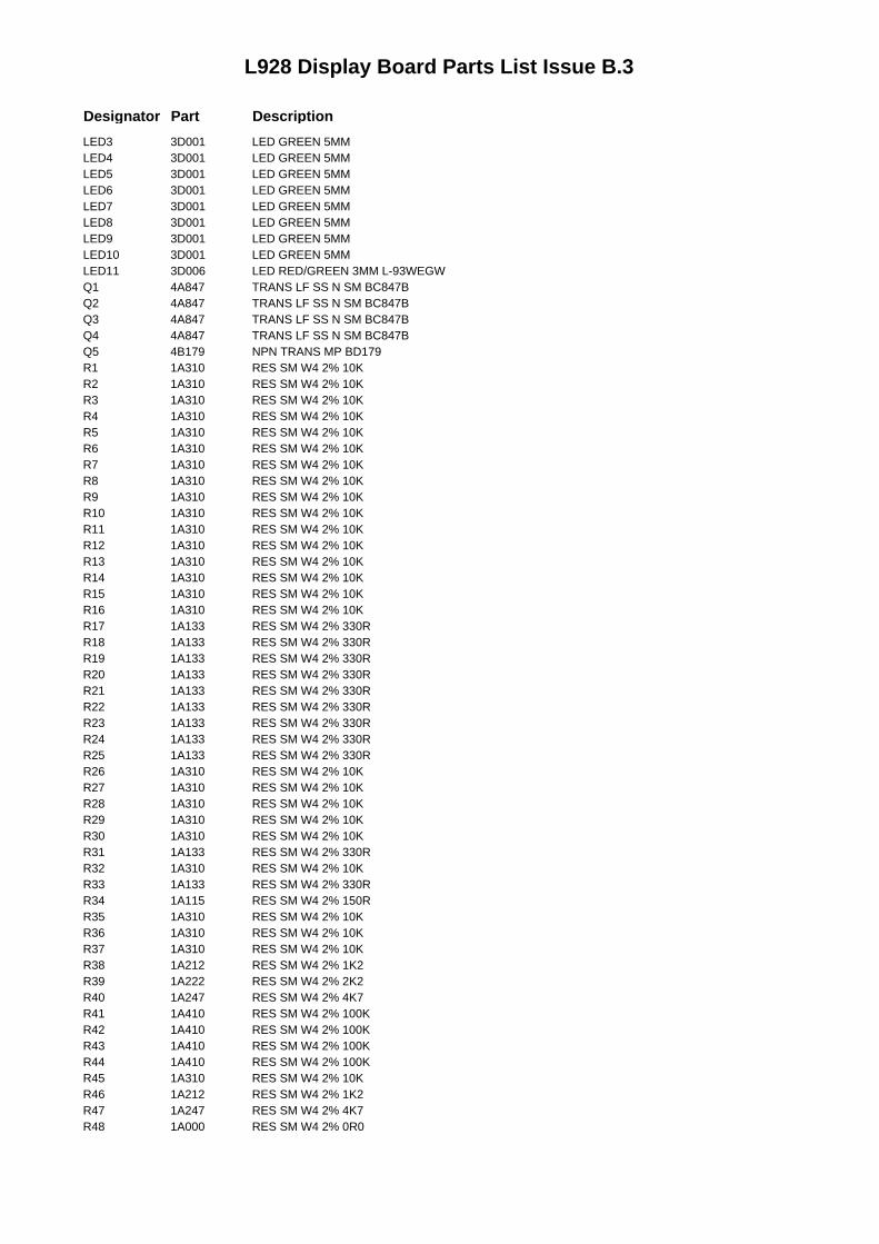
L928 Display Board Parts List Issue B.3
Designator Part DescriptionLED3 3D001 LED GREEN 5MMLED4 3D001 LED GREEN 5MMLED5 3D001 LED GREEN 5MMLED6 3D001 LED GREEN 5MMLED7 3D001 LED GREEN 5MMLED8 3D001 LED GREEN 5MMLED9 3D001 LED GREEN 5MMLED10 3D001 LED GREEN 5MMLED11 3D006 LED RED/GREEN 3MM L-93WEGWQ1 4A847 TRANS LF SS N SM BC847BQ2 4A847 TRANS LF SS N SM BC847BQ3 4A847 TRANS LF SS N SM BC847BQ4 4A847 TRANS LF SS N SM BC847BQ5 4B179 NPN TRANS MP BD179R1 1A310 RES SM W4 2% 10KR2 1A310 RES SM W4 2% 10KR3 1A310 RES SM W4 2% 10KR4 1A310 RES SM W4 2% 10KR5 1A310 RES SM W4 2% 10KR6 1A310 RES SM W4 2% 10KR7 1A310 RES SM W4 2% 10KR8 1A310 RES SM W4 2% 10KR9 1A310 RES SM W4 2% 10KR10 1A310 RES SM W4 2% 10KR11 1A310 RES SM W4 2% 10KR12 1A310 RES SM W4 2% 10KR13 1A310 RES SM W4 2% 10KR14 1A310 RES SM W4 2% 10KR15 1A310 RES SM W4 2% 10KR16 1A310 RES SM W4 2% 10KR17 1A133 RES SM W4 2% 330RR18 1A133 RES SM W4 2% 330RR19 1A133 RES SM W4 2% 330RR20 1A133 RES SM W4 2% 330RR21 1A133 RES SM W4 2% 330RR22 1A133 RES SM W4 2% 330RR23 1A133 RES SM W4 2% 330RR24 1A133 RES SM W4 2% 330RR25 1A133 RES SM W4 2% 330RR26 1A310 RES SM W4 2% 10KR27 1A310 RES SM W4 2% 10KR28 1A310 RES SM W4 2% 10KR29 1A310 RES SM W4 2% 10KR30 1A310 RES SM W4 2% 10KR31 1A133 RES SM W4 2% 330RR32 1A310 RES SM W4 2% 10KR33 1A133 RES SM W4 2% 330RR34 1A115 RES SM W4 2% 150RR35 1A310 RES SM W4 2% 10KR36 1A310 RES SM W4 2% 10KR37 1A310 RES SM W4 2% 10KR38 1A212 RES SM W4 2% 1K2R39 1A222 RES SM W4 2% 2K2R40 1A247 RES SM W4 2% 4K7R41 1A410 RES SM W4 2% 100KR42 1A410 RES SM W4 2% 100KR43 1A410 RES SM W4 2% 100KR44 1A410 RES SM W4 2% 100KR45 1A310 RES SM W4 2% 10KR46 1A212 RES SM W4 2% 1K2R47 1A247 RES SM W4 2% 4K7R48 1A000 RES SM W4 2% 0R0
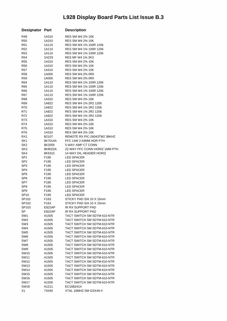
L928 Display Board Parts List Issue B.3
Designator Part DescriptionR49 1A310 RES SM W4 2% 10KR50 1A310 RES SM W4 2% 10KR51 1A110 RES SM W4 1% 100R 1206R52 1A110 RES SM W4 1% 100R 1206R53 1A110 RES SM W4 1% 100R 1206R54 1H233 RES MF W4 1% 3K3R55 1A310 RES SM W4 2% 10KR56 1A310 RES SM W4 2% 10KR57 1A310 RES SM W4 2% 10KR58 1A000 RES SM W4 2% 0R0R59 1A000 RES SM W4 2% 0R0R64 1A110 RES SM W4 1% 100R 1206R65 1A110 RES SM W4 1% 100R 1206R66 1A110 RES SM W4 1% 100R 1206R67 1A110 RES SM W4 1% 100R 1206R68 1A310 RES SM W4 2% 10KR69 1A822 RES SM W4 1% 2R2 1206R70 1A822 RES SM W4 1% 2R2 1206R71 1A822 RES SM W4 1% 2R2 1206R72 1A822 RES SM W4 1% 2R2 1206R73 1A310 RES SM W4 2% 10KR74 1A310 RES SM W4 2% 10KR75 1A310 RES SM W4 2% 10KR76 1A310 RES SM W4 2% 10KRX1 B2107 REMOTE RX PIC-26043TM2 38KHZSK1 8K7014A FFC 14W 2.54MM HOR PTHSK2 8K2005 5-WAY AMP CT CONNSK3 8K8022A 22-WAY FFC CONN HORIZ 1MM PTHSK4 8K6315 14 WAY DIL HEADER HORIZSP1 F195 LED SPACERSP2 F195 LED SPACERSP3 F195 LED SPACERSP4 F195 LED SPACERSP5 F195 LED SPACERSP6 F195 LED SPACERSP7 F195 LED SPACERSP8 F195 LED SPACERSP9 F195 LED SPACERSP10 F195 LED SPACERSP101 F163 STICKY PAD S/A 10 X 15mmSP102 F163 STICKY PAD S/A 10 X 15mmSP103 E822AP IR RX SUPPORT PADSP E822AP IR RX SUPPORT PADSW1 A1505 TACT SWITCH SM SDTM-610-NTRSW2 A1505 TACT SWITCH SM SDTM-610-NTRSW3 A1505 TACT SWITCH SM SDTM-610-NTRSW4 A1505 TACT SWITCH SM SDTM-610-NTRSW5 A1505 TACT SWITCH SM SDTM-610-NTRSW6 A1505 TACT SWITCH SM SDTM-610-NTRSW7 A1505 TACT SWITCH SM SDTM-610-NTRSW8 A1505 TACT SWITCH SM SDTM-610-NTRSW9 A1505 TACT SWITCH SM SDTM-610-NTRSW10 A1505 TACT SWITCH SM SDTM-610-NTRSW11 A1505 TACT SWITCH SM SDTM-610-NTRSW12 A1505 TACT SWITCH SM SDTM-610-NTRSW13 A1505 TACT SWITCH SM SDTM-610-NTRSW14 A1505 TACT SWITCH SM SDTM-610-NTRSW15 A1505 TACT SWITCH SM SDTM-610-NTRSW16 A1505 TACT SWITCH SM SDTM-610-NTRSW17 A1505 TACT SWITCH SM SDTM-610-NTRSW18 A1211 EC16B2414X1 7X040 XTAL 16MHZ SM GSX49-4
1 2 3 4 5 6 7 8
A
B
C
D
87654321
D
C
B
A
ISSUE
DRAWING NO.
23425
DRAWING TITLE
Drawn by:DATE
FilenameECO No. DESCRIPTION OF CHANGE
J:\Released_Documents\Native_format_files\Protel_DDB\L928_B.3.Ddb - Documents\L928CT_1_B.3.PRJ
A & R Cambridge Ltd.Pembroke AvenueDenny Industrial CentreWaterbeachCambridge CB5 9PB
A32 FMJ AMP DISPLAY PCB
Circuit Diagram
L928CT1CL10-Oct-2001
INITIALSDate Printed 1 2Sheet of
Notes:
L928CT_B.1L928CT_2_B.3.SCH
FD_1
FIDUCIAL
FD_2
FIDUCIAL
A32 FMJ DISPLAY PCB
MICRO
PCB
PCB1
L928PB_B
CHASSIS 1
CHASSIS 2
CHASSIS 3
(BY SK3)
(BY SK1)
(BY SK2)
C391N0 SM
C451N0 SM
C401N0 SM
C411N0 SM
C431N0 SM
C441N0 SM
C461N0 SM
C471N0 SM C49
1N0 SMC481N0 SM
0V_D
0V_D 0V_D 0V_D 0V_D
0V_D0V_D0V_D0V_D
0V_D
CL INITIAL PROTOTYPE25/04/01 A.0
FIX2FIXING HOLE 3.5
FIX7FIXING HOLE 3.5
FIX10FIXING HOLE 3.5
FIX5FIXING HOLE 3.5
FIX11FIXING HOLE 3.5
FIX13FIXING HOLE 3.5
FIX3FIXING HOLE 3.5
FIX8FIXING HOLE 3.5
FIX1FIXING HOLE 3.5
FIX6FIXING HOLE 3.5
FIX9FIXING HOLE 3.2
FIX12FIXING HOLE 3.2
C381N0 SM
C371N0 SM
0V_D
0V_D
WAF 9/08/01 UPDATED PROTOTYPE B.0
JBR 10/9/01 PRE PRODUCTION RELEASE B.2
WAF 26/9/01 STICKY PADS RENUMBERED B.3
1 2 3 4 5 6 7 8
A
B
C
D
87654321
D
C
B
A
ISSUE
DRAWING NO.
23425
DRAWING TITLE
Drawn by:DATE
FilenameECO No. DESCRIPTION OF CHANGE
J:\Released_Documents\Native_format_files\Protel_DDB\L928_B.3.Ddb - Documents\L928CT_2_B.3.SCH
A & R Cambridge Ltd.Pembroke AvenueDenny Industrial CentreWaterbeachCambridge CB5 9PB
A32 FMJ AMP DISPLAY PCB
Circuit Diagram
L928CT2CL10-Oct-2001
INITIALSDate Printed 2 2Sheet of
Notes:
Vcc1
PB02
PB13
PB24
PB35
PB46
PB57
PB68
PB79
Vpp/RESO10
Vss11
TxD0/P9.012
TxD1/P9.113
RxD0/P9.214
RxD1/P9.315
IRQ4/SCK0/P9.416
IRQ5/SCK1/P9.517
D0/P4.018
D1/P4.119
D2/P4.220
D3/P4.321
Vss22
D4/P4.423
D5/P4.524
D6/P4.625
D7/
P4.7
26
D8/
P3.0
27
D9/
P3.1
28
D10
/P3.
229
D11
/P3.
330
D12
/P3.
431
D13
/P3.
532
D14
/P3.
633
D15
/P3.
734
Vcc
35
A0/
P1.0
36
A1/
P1.1
37
A2/
P1.2
38
A3/
P1.3
39
A4/
P1.4
40
A5/
P1.5
41
A6/
P1.6
42
A7/
P1.7
43
Vss
44
A8/
P2.0
45
A9/
P2.1
46
A10
/P2.
247
A11
/P2.
348
A12
/P2.
449
A13
/P2.
550
P2.6/A14 51P2.7/A15 52P5.0/A16 53P5.1/A17 54P5.2/A18 55P5.3/A19 56Vss 57P6.0/WAIT 58P6.1/BREQ 59P6.2/BACK 60CLKOUT 61STBY 62RES 63NM1 64Vss 65EXTAL 66XTAL 67Vcc 68P6.3/AS 69P6.4/RD 70P6.5/HWR 71P6.6/LWR 72MD0 73MD1 74MD2 75
AV
cc76
Vre
f77
P7.0
/AN
078
P7.1
/AN
179
P7.2
/AN
280
P7.3
/AN
381
P7.4
/AN
482
P7.5
/AN
583
P7.6
/AN
6/D
A0
84P7
.7/A
N7/
DA
185
AV
ss86
P8.0
/IRQ
087
P8.1
/IRQ
188
P8.2
/IRQ
289
P8.3
/IRQ
390
P8.4
/CS0
91V
ss92
PA0
93PA
194
PA2
95PA
396
PA4
97PA
598
PA6
99PA
710
0
H8/3048F
IC1
H8/3048F
Gnd1
Res2 Vcc3
DS1
233
Gnd4
IC2
DS1233 SM
R110K SM
R210K SM
R310K SM
R410K SM
R510K SM
R610K SM
R710K SM
R810K SM
R910K SM
R1010K SM
R1110K SM
R1210K SM
R1310K SM
R1410K SM
R1510K SM
R1610K SM
0V_D
R17330R SM
R18330R SM
R19330R SM
R21330R SM
R22330R SM
R25330R SM
BUT1
1
BUT2
BUT3
BUT4
BUT1
3
BUT6
BUT7
BUT8
BUT9
BUT1
2
BUT1
4
BUT1
BUT1
0
BUT5
BUT1
5
BUT1
6
0V_D
C118P SM
C218P SM
Programming adaptor
+5V
0V_D
+5V
+5V
D2BAS16W SM
+5V
R26
10K SM
+5V
IND
10
IND
2
IND
8
IND
1
IND
5
IND
6
IND
9
IND
4
IND
3
IND
7
0V_D
+5V
R27
10K
SM
R28
10K
SM
R34150R SM
R33330R SM
0V_D
+5V
0V_D
+5V
To preamp board
SEL1SEL2SEL3SEL4SEL5SEL6SEL7SEL8SEL9
LEFTAUDIO
MUTETONE
TONEID
SDATA
SLOAD
SCLK
0V_D
PHASEAPHASEB
+5V
PHAS
EAPH
ASEB
+5V
0V_D
A0
1A
12
A2
3
VSS4 SDA
5
SCL
6
WP
7
VDD 8
IC524C02 SM
0V_D
R3210K SM
+5V
DISPCLK
DISPDAT
DIS
PDAT
DIS
PCLK
0V_D
F1 to F2 = 4Vac 150mAVDD2 = 40Vdc 20mA
+5V
DIS
PLAT
DIS
PBLK
3
21
IC6A
LM393A SM
5
67
IC6B
LM393A SM
84
IC6CLM393A SM
C3100N SM
C4100N SM
0V_D
0V_D
C5100N SM
0V_D
DISPBLKDISPLAT
BUT9BUT8BUT7BUT6BUT2IND3
BUT3
BUT1
IND
1BU
T5IN
D2
BUT4
IND
12IN
D11
BUT1
6IN
D6
BUT1
5IN
D5
BUT1
0IN
D7
BUT1
2IN
D9
BUT1
4IN
D4
BUT1
1IN
D8
BUT1
3
C6100N SM
C7
100N SM
C8100N SM
C9
100N SM
C10100N SM
0V_D
+5V
R35
10K SM
R36
10K SM
R3710K SM
R381K2 SM
R39
2K2 SM
R404K7 SM
+5V
+5V
+5V
0V_D
0V_D
+ C1110U EL SM
R41100K SM
R42100K SM
0V_D
+5V
R43100K SM
R44100K SM
3
21
IC7ALM393A SM
5
67
IC7B
LM393A SM
84
IC7CLM393A SM
0V52V7
2V7
0V5
3
21
IC8A
LM393A SM
5
67
IC8B
LM393A SM
84
IC8CLM393A SM
R4510K SM
R461K2 SM
R474K7 SM
0V5
2V7+5V
+5V
0V_D
0V_D
R48
0R0
SM
SCLKSLOAD
SDATATONEID
SEL1SEL2SEL3SEL4SEL5SEL6SEL7
SEL8
SEL9
MU
TETO
NE
+ C1410U EL SM
C15100N SM
0V_D
C16100N SM
12345
SK2
AMPCT5
SAMTX2
SAMRX2
SAMRX2SAMTX2
SAMBUSYSAMDATA
+5V
0V_D
IND
10
C17100N SM
0V_D
D3BAS16W SM
R5510K SM
+5V
PR_TXDPR_GND
PR_RESETPR_MD
PR_PMODEPR_VPP
PR_RXDPR_VCC
VFD_VDD2
3
21
IC11AAD8532 SM
5
67
IC11BAD8532 SM
84
IC11CAD8532 SM C25
100N SM
DC
PRO
TVI
PRO
T
F1C
LOC
KF2
CLO
CK
STANDBYSP1ONSP2ONTHERMPROT
+5V
0V_D
F1CLOCK
F2CLOCK
+SUP VFD_VDD2
+
C2810U EL SM
0V_D
R5610K SM
R5710K SM
Q_1Q_2Q_3Q_4Q_5Q_6Q_7Q_8Q_9
Q_10
Q_11Q_12
Q_14
Q_15
Q_16
Q_17
Q_19
Q_20
Q_21 Q_22
Q_23
R58
0R0 SM
R59
0R0 SM
R64100R SM
R65
100R SM R66100R SMR67
100R SM
C3110P SM
C3210P SM
0V_D
R4910K SM
R5010K SM
+5V
Q_34SAMHOLD
SAMHOLD
R51100R SM
Q_35
Q_37
Q_38
Q_39
Q_40Q_41
Q_42
Q_43
Q_44
Q_45
Q_46
Q_47Q_48
Q_49
Q_50
Q_51
Q_52
Q_53Q_54
Q_55
Q_56
Q_57
Q_58
Q_59
Q_64
Q_65 Q_66 Q_67 Q_68 Q_69 Q_70 Q_71 Q_72 Q_73 Q_74
Q_75
Q_78
Q_79 Q_80
Q_81
Q_82
Q_8
3Q
_84
Q_8
5
Q_86Q_87Q_88Q_89Q_90Q_91
Q_9
2Q
_93
Q_9
4Q
_95
Q_9
6Q
_97
Q_98
Q_9
9Q
_100
Q_1
01Q
_102
Q_1
03Q
_104
Q_1
05Q
_106
Q_1
07Q
_108
Q_1
09Q
_110
Q_1
11Q
_112
Q_1
13Q
_114
Q_115
Q_116
R20330R SM
R23330R SM
R24330R SM
R31330R SM
R G
LED11
LED RED/GRN 3MM
Q1BC847B
Q2BC847B
R2910K SM R30
10K SM
0V_D
IND
11
IND
12
R6810K SM
BUT1
7
BUT17
0V_D
+5V
+SUP
STANDBYSP1ONSP2ONTHERMPROTVIPROTDCPROTACPRESENT
ACPR
ESEN
T
0V_D
R69
2R2
SM
R70
2R2
SM
R71
2R2
SM
R72
2R2
SM
0V_D
IRIN
Q3BC847B
Q4BC847B
R7310K SM
R7410K SM
R7510K SM
R76
10K SM
0V_D
+5V
IRIN
IRIN
IROUT
C12
100N SM
(FIT CLOSE TO SK1)
+5V
0V_D
+ C33220U EL
+ C34220U EL
SAMDATASAMBUSY
IRIN
C 3
B 2A 1
4 5
SW18ALPS_ENCODER
LED7
LED GREEN
LED8
LED GREEN
LED6
LED GREEN
LED3
LED GREEN
LED10
LED GREEN
LED9
LED GREEN
LED1
LED GREEN
LED4
LED GREEN
LED2
LED GREEN
LED5
LED GREEN
RECEIVE
TRANSMIT
TRANSMIT
TRANSMIT
RECEIVE
RECEIVE
RESPIN
RESPIN
PB0
PB0
VPROG
VPROG
1234567891011121314
SK1
FFC 14W 2.54MM HOR
12345678910111213141516171819202122
SK3
FFC 22W 1MM HOR
To power amp / PSU
0V_D
C50A 100PX4 SMC50B 100PX4 SM
C50C 100PX4 SMC50D 100PX4 SM
C51A 100PX4 SMC51B 100PX4 SM
C51C 100PX4 SMC51D 100PX4 SM
C52A 100PX4 SMC52B 100PX4 SM
C52C 100PX4 SMC52D 100PX4 SM
C53A 100PX4 SMC53B 100PX4 SM
C53C 100PX4 SMC53D 100PX4 SM
C54A 100PX4 SMC54B 100PX4 SM
C54C 100PX4 SMC54D 100PX4 SM
C55A 100PX4 SMC55B 100PX4 SM
CHASSIS 1
C60D 100PX4 SMC60C 100PX4 SM
C60B 100PX4 SMC60A 100PX4 SM
C61D 100PX4 SMC61C 100PX4 SM
C61B 100PX4 SMC61A 100PX4 SM
C62D 100PX4 SMC62C 100PX4 SM
C62B 100PX4 SMC62A 100PX4 SM
C63D 100PX4 SMC63C 100PX4 SM
CHASSIS 2
+ C29100U EL SM
R52
100R SM
R53
100R SM
LEFTAUDIO
+
C2610U EL SM
C55C 100PX4 SMC55D 100PX4 SM
C63B 100PX4 SM
C63A 100PX4 SM
X116MHZ SM
F11
F12
F13
SIN
4
VD
D1
5
SOU
T6
LAT
7
BLK
8
CLK
9
VSS
10
VSS
11
VD
D2
12
F215
F216
F217
Graphics Display
DISP1B1013
12345678910
11121314
SK4
HEADER 7X2HORIZ
STICKY PADDOUBLE SIDED
10 X 15MM
SP101
STICKY PAD DS 10X15MM
STICKY PADDOUBLE SIDED
10 X 15MM
SP102
STICKY PAD DS 10X15MM
Q_122Q_123Q_124Q_125Q_126Q_127Q_128
Q_129
Q_120
Q_119
Q_118
Q_117
Q_121
CL 25/04/01 INITIAL PROTOTYPE A.0
+5V
3
O/P2
GN
D1
Cas
eC
ase
O/P
GN
D+5
V
RX1SBX1610-52/PIC-26043TM2
Q5BD179 NPN TO-126
R543K3 MF
DISPLAY CRADLEE916PM
DC1
DISPLAY CRADLE E916PM
DISPLAY CRADLEE916PM
DC2
DISPLAY CRADLE E916PM
SW6TACTSW A1505
SW12TACTSW A1505
SW11TACTSW A1505
SW8TACTSW A1505
SW7TACTSW A1505
SW13TACTSW A1505
SW14TACTSW A1505
SW15TACTSW A1505
SW16TACTSW A1505
SW17TACTSW A1505
SW1TACTSW A1505
SW2TACTSW A1505
SW3TACTSW A1505
SW4TACTSW A1505
SW5TACTSW A1505
SW9TACTSW A1505
SW10TACTSW A1505
POWER SP1SP2TONE DOWN UP ENTERMODE RECORD SELECT
C13
100N SM
AV DVD CD TUNER VCRPHONO/
AUX TAPE
IR RXSUPPORT PAD
SP
IR RX SUPPORT PAD
LED
SPAC
ER
SP1
SPACER F195
LED
SPAC
ER
SP2
SPACER F195
LED
SPAC
ER
SP3
SPACER F195
LED
SPAC
ER
SP4
SPACER F195
LED
SPAC
ER
SP5
SPACER F195
LED
SPAC
ER
SP6
SPACER F195
LED
SPAC
ER
SP7
SPACER F195
LED
SPAC
ER
SP8
SPACER F195
LED
SPAC
ER
SP9
SPACER F195
LED
SPAC
ER
SP10
SPACER F195
WAF 9/08/01 UPDATED PROTOTYPE B.0
IR RXSUPPORT PAD
SP103
IR RX SUPPORT PAD
PLACE ONE ON TOP OFTHE OTHER UNDER RX1
D1ZENER 400MW 33V
JBR 10/9/01 PRE PRODUCTION RELEASE B.2
WAF 26/9/01 STICKY PADS RENUMBERED B.3
Preamplifier Board L937
Contents
! Circuit description
! Component overlay
! Parts list
! Circuit diagrams
Pre-amplifier circuit description Refer to L937 circuit diagrams The A32 preamplifier is a high-performance, DC coupled design with microprocessor control of input select, two independent tape loops, electronic volume control, tone bypass and electronic tone control. It features a discrete power supply and low-noise linear circuitry to obtain very good distortion and noise performance, suitable for high quality source material such as CD or DVD-A. Input switching Each of the inputs has a pair of diodes to the ±15V rails to prevent static spikes from causing damage to the CMOS multiplexers. In addition, there is a simple resistor-capacitor filter with a corner frequency of approximately 340kHz to remove any unwanted high frequency interference from the signal. This uses high-quality polypropylene capacitors for best performance. Z104 and Z105 are the main input select multiplexers, which are configured in a ‘virtual earth’ unity gain arrangement with Z115 and Z116. This arrangement is slightly lower distortion than the ‘normal’ one, at the cost of a slightly higher noise floor. It is an inverting configuration, which is restored to correct polarity by the inverting electronic volume control which follows. Z115B and Z116B are integrating servos, which take out any DC from the input signal before the following stages. The servos are 2-pole, with a passive 2 nd pole being formed by R180 and C147 (for the left channel) to remove broadband noise from the output of the servo and improve speed of response. Z100 thru Z103 are the input selectors for the 2 tape loops. These are normal non-inverting selectors which are buffered before being passed on to the phono sockets. Z109A output is decoupled by R108 which is included in the feedback path. Local high frequency feedback occurs around C108 to allow the tape loop output to be very low impedance, whilst being stable into a capacitive load such as may be presented by a screened interconnect cable. This is the same for all tape outputs. Z106 is configured as a double pole changeover switch, used to select the tone controls. The tone controls are bypassed when not required so that the noise and distortion can be minimised. Tone control circuit The tone control circuit is a non-inverting one, using a gyrated ‘bell’ filter for the bass and a simple shelving filter for the treble. Left channel description The input is attenuated by 6dB and biased to a voltage of +2.5V DC by C111, R113, R112, R110, R111 and C110. This is so the signals fall within the 0 - 5VDC required by the digital potentiometer Z108. Z111B and its associated components form an active equivalent of a series resonant LCR circuit. This has an impedance minimum of 5.4k˜ at around 80Hz with Q=0.7 The reason the bass is done as a band-boost filter rather than a shelving filter is so that you can boost the ‘real’ bass without causing lots of sub-audio loudspeaker cone
excursion which wastes power and may damage the drive units. The digital pots Z108D and Z108A control the bass and treble respectively. This is done by moving the wiper connected to the frequency-sensitive impedance between the non-inverting and inverting terminals of Z112A, effectively changing the ratio of feedback boost and feed-forward attenuation of the circuit at the desired frequencies, thus providing a EQ gain control that is symmetrical on a logarithmic scale, with the use of a linear pot. Z112B provides the 6dB of gain necessary to bring the nominal signal level back to unity. C116 and C117 remove the 2.5VDC offset from the output, to prevent clunks when the tone controls are activated. Z108 is controlled by a simple 3-wire serial interface from the microprocessor. Each of the digital lines has its own ground return to minimise electromagnetic interference. They are connected together only at the GND pin of the IC. Volume control Z107 is a VSDVC electronic volume control IC. It works, in conjunction with an external op-amp, by varying the feed-forward and feedback resistors in an inverting gain configuration. In this way, it can allow output signal swings of up to 22Vpp whilst operating from a single +5VDC power supply. Also, it allows the user the choice of external circuitry to fine-tune the performance. The gain is controlled from the microprocessor via a 3-wire serial interface. The analogue supply rail is derived from the local +5V via R185 and C156 // C157. Z117 is the output op-amp. Its outputs are decoupled via R186, R187, C158 and C159 so that it has a low output impedance but can drive cable capacitance without oscillation. R186 and R187 are included in the audio frequency feedback loop to reduce output impedance when driving ‘difficult’ cables. RLY100 is a mute relay which shunts the preamp output to ground. This is to prevent thumps and squeals when the units is powered up or down. Power supply The transformer winding is connected to SK300. The voltage is rectified and smoothed by D300, D301, D306, D307 and C300, C310. The unregulated voltage should be around ±27VDC. F300 and F301 are secondary fuses, as the low power preamp winding would not blow the primary fuses if short circuited. The voltage regulators are discrete compound emitter followers. I will describe the +15V supply as the negative is essentially an exact mirror image. Q300 and R300 act as a constant current source, supplying around 7mA into D310. C302 and C314 reduce ripple and broadband noise on the zener diode. Q305 and Q306 form a complementary Darlington NPN transistor which is configured as an emitter follower, producing the +15VDC at its output. C303 is to provide bulk charge storage and to reduce the AC output impedance of the power supply. D302 prevents reverse bias of the supply during power down. Z301 is a conventional LM317 type circuit to drop the +15V rail down to +5V for the tone and volume control circuits. Star point SP300 explicitly connects the differently named ground nets together at one point, to minimise hum.
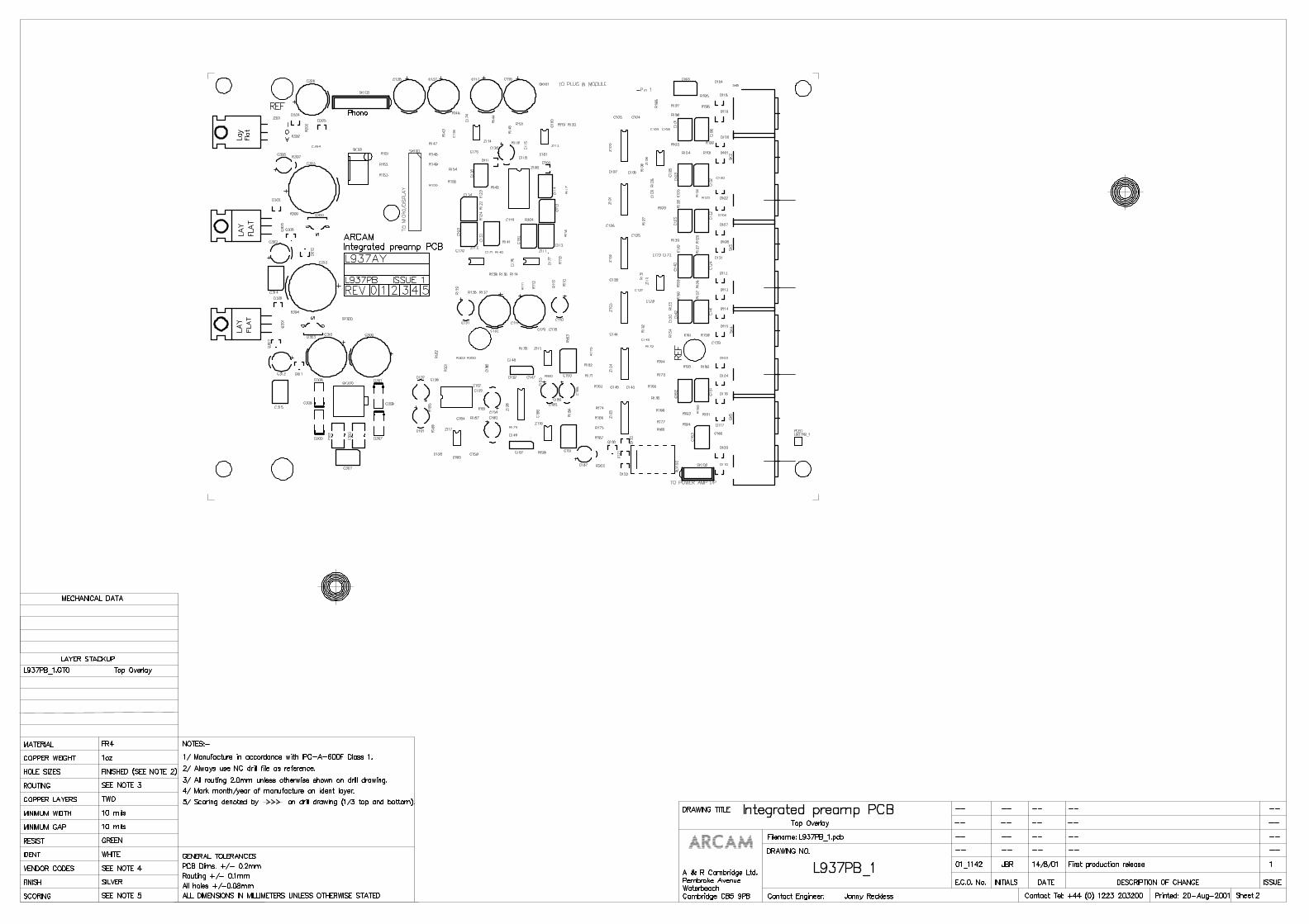
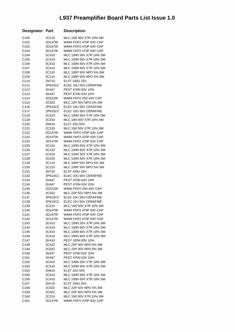
L937 Preamplifier Board Parts List Issue 1.0
Designator Part DescriptionC100 2C210 MLC 1N0 50V X7R 10% SMC101 2D147W WIMA FKP2 470P 63V CAPC102 2D147W WIMA FKP2 470P 63V CAPC103 2D147W WIMA FKP2 470P 63V CAPC104 2C410 MLC 100N 50V X7R 10% SMC105 2C410 MLC 100N 50V X7R 10% SMC106 2C410 MLC 100N 50V X7R 10% SMC107 2C410 MLC 100N 50V X7R 10% SMC108 2C110 MLC 100P 50V NPO 5% SMC109 2C110 MLC 100P 50V NPO 5% SMC110 2N710 ELST 100U 25VC111 2P610CC ELEC 10U 50V CERAFINEC112 2K447 PEST 470N 63V 10%C113 2K447 PEST 470N 63V 10%C114 2D222W WIMA FKP2 2N2 63V CAPC115 2C022 MLC 22P 50V NPO 5% SMC116 2P610CC ELEC 10U 50V CERAFINEC117 2P610CC ELEC 10U 50V CERAFINEC118 2C410 MLC 100N 50V X7R 10% SMC119 2C310 MLC 10N 50V X7R 10% SMC120 2N610 ELST 10U 50VC121 2C210 MLC 1N0 50V X7R 10% SMC122 2D147W WIMA FKP2 470P 63V CAPC123 2D147W WIMA FKP2 470P 63V CAPC124 2D147W WIMA FKP2 470P 63V CAPC125 2C410 MLC 100N 50V X7R 10% SMC126 2C410 MLC 100N 50V X7R 10% SMC127 2C410 MLC 100N 50V X7R 10% SMC128 2C410 MLC 100N 50V X7R 10% SMC129 2C110 MLC 100P 50V NPO 5% SMC130 2C110 MLC 100P 50V NPO 5% SMC131 2N710 ELST 100U 25VC132 2P610CC ELEC 10U 50V CERAFINEC133 2K447 PEST 470N 63V 10%C134 2K447 PEST 470N 63V 10%C135 2D222W WIMA FKP2 2N2 63V CAPC136 2C022 MLC 22P 50V NPO 5% SMC137 2P610CC ELEC 10U 50V CERAFINEC138 2P610CC ELEC 10U 50V CERAFINEC139 2C210 MLC 1N0 50V X7R 10% SMC140 2D147W WIMA FKP2 470P 63V CAPC141 2D147W WIMA FKP2 470P 63V CAPC142 2D147W WIMA FKP2 470P 63V CAPC143 2C410 MLC 100N 50V X7R 10% SMC144 2C410 MLC 100N 50V X7R 10% SMC145 2C410 MLC 100N 50V X7R 10% SMC146 2C410 MLC 100N 50V X7R 10% SMC147 2K410 PEST 100N 63V 10%C148 2C022 MLC 22P 50V NPO 5% SMC149 2C022 MLC 22P 50V NPO 5% SMC150 2K447 PEST 470N 63V 10%C151 2K447 PEST 470N 63V 10%C152 2C410 MLC 100N 50V X7R 10% SMC153 2C410 MLC 100N 50V X7R 10% SMC154 2N610 ELST 10U 50VC155 2C410 MLC 100N 50V X7R 10% SMC156 2C410 MLC 100N 50V X7R 10% SMC157 2N710 ELST 100U 25VC158 2C022 MLC 22P 50V NPO 5% SMC159 2C022 MLC 22P 50V NPO 5% SMC160 2C210 MLC 1N0 50V X7R 10% SMC161 2D147W WIMA FKP2 470P 63V CAP
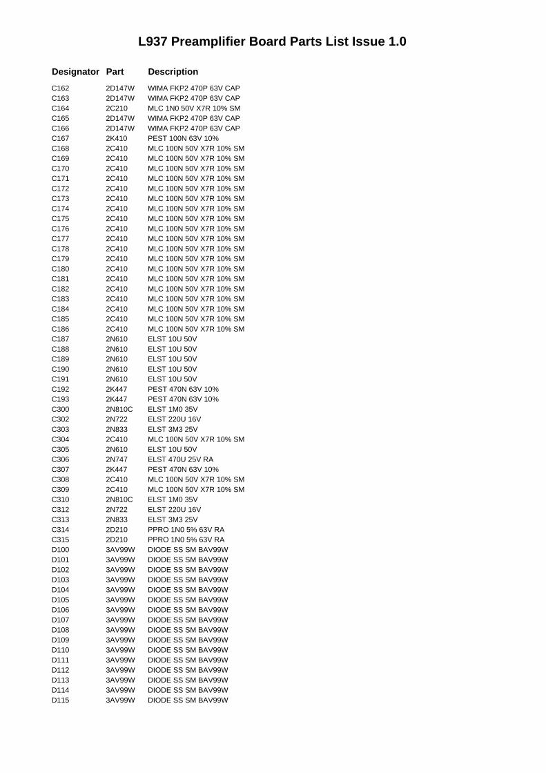
L937 Preamplifier Board Parts List Issue 1.0
Designator Part DescriptionC162 2D147W WIMA FKP2 470P 63V CAPC163 2D147W WIMA FKP2 470P 63V CAPC164 2C210 MLC 1N0 50V X7R 10% SMC165 2D147W WIMA FKP2 470P 63V CAPC166 2D147W WIMA FKP2 470P 63V CAPC167 2K410 PEST 100N 63V 10%C168 2C410 MLC 100N 50V X7R 10% SMC169 2C410 MLC 100N 50V X7R 10% SMC170 2C410 MLC 100N 50V X7R 10% SMC171 2C410 MLC 100N 50V X7R 10% SMC172 2C410 MLC 100N 50V X7R 10% SMC173 2C410 MLC 100N 50V X7R 10% SMC174 2C410 MLC 100N 50V X7R 10% SMC175 2C410 MLC 100N 50V X7R 10% SMC176 2C410 MLC 100N 50V X7R 10% SMC177 2C410 MLC 100N 50V X7R 10% SMC178 2C410 MLC 100N 50V X7R 10% SMC179 2C410 MLC 100N 50V X7R 10% SMC180 2C410 MLC 100N 50V X7R 10% SMC181 2C410 MLC 100N 50V X7R 10% SMC182 2C410 MLC 100N 50V X7R 10% SMC183 2C410 MLC 100N 50V X7R 10% SMC184 2C410 MLC 100N 50V X7R 10% SMC185 2C410 MLC 100N 50V X7R 10% SMC186 2C410 MLC 100N 50V X7R 10% SMC187 2N610 ELST 10U 50VC188 2N610 ELST 10U 50VC189 2N610 ELST 10U 50VC190 2N610 ELST 10U 50VC191 2N610 ELST 10U 50VC192 2K447 PEST 470N 63V 10%C193 2K447 PEST 470N 63V 10%C300 2N810C ELST 1M0 35VC302 2N722 ELST 220U 16VC303 2N833 ELST 3M3 25VC304 2C410 MLC 100N 50V X7R 10% SMC305 2N610 ELST 10U 50VC306 2N747 ELST 470U 25V RAC307 2K447 PEST 470N 63V 10%C308 2C410 MLC 100N 50V X7R 10% SMC309 2C410 MLC 100N 50V X7R 10% SMC310 2N810C ELST 1M0 35VC312 2N722 ELST 220U 16VC313 2N833 ELST 3M3 25VC314 2D210 PPRO 1N0 5% 63V RAC315 2D210 PPRO 1N0 5% 63V RAD100 3AV99W DIODE SS SM BAV99WD101 3AV99W DIODE SS SM BAV99WD102 3AV99W DIODE SS SM BAV99WD103 3AV99W DIODE SS SM BAV99WD104 3AV99W DIODE SS SM BAV99WD105 3AV99W DIODE SS SM BAV99WD106 3AV99W DIODE SS SM BAV99WD107 3AV99W DIODE SS SM BAV99WD108 3AV99W DIODE SS SM BAV99WD109 3AV99W DIODE SS SM BAV99WD110 3AV99W DIODE SS SM BAV99WD111 3AV99W DIODE SS SM BAV99WD112 3AV99W DIODE SS SM BAV99WD113 3AV99W DIODE SS SM BAV99WD114 3AV99W DIODE SS SM BAV99WD115 3AV99W DIODE SS SM BAV99W
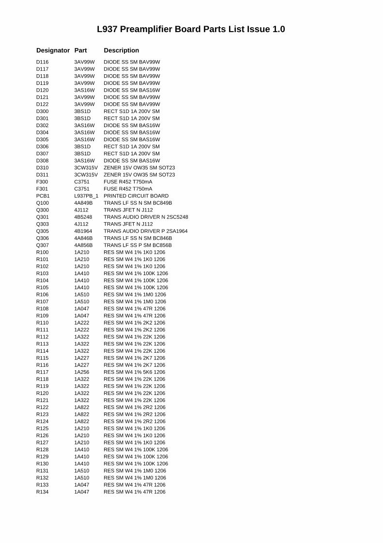
L937 Preamplifier Board Parts List Issue 1.0
Designator Part DescriptionD116 3AV99W DIODE SS SM BAV99WD117 3AV99W DIODE SS SM BAV99WD118 3AV99W DIODE SS SM BAV99WD119 3AV99W DIODE SS SM BAV99WD120 3AS16W DIODE SS SM BAS16WD121 3AV99W DIODE SS SM BAV99WD122 3AV99W DIODE SS SM BAV99WD300 3BS1D RECT S1D 1A 200V SMD301 3BS1D RECT S1D 1A 200V SMD302 3AS16W DIODE SS SM BAS16WD304 3AS16W DIODE SS SM BAS16WD305 3AS16W DIODE SS SM BAS16WD306 3BS1D RECT S1D 1A 200V SMD307 3BS1D RECT S1D 1A 200V SMD308 3AS16W DIODE SS SM BAS16WD310 3CW315V ZENER 15V OW35 SM SOT23D311 3CW315V ZENER 15V OW35 SM SOT23F300 C3751 FUSE R452 T750mAF301 C3751 FUSE R452 T750mAPCB1 L937PB_1 PRINTED CIRCUIT BOARDQ100 4A849B TRANS LF SS N SM BC849BQ300 4J112 TRANS JFET N J112Q301 4B5248 TRANS AUDIO DRIVER N 2SC5248Q303 4J112 TRANS JFET N J112Q305 4B1964 TRANS AUDIO DRIVER P 2SA1964Q306 4A846B TRANS LF SS N SM BC846BQ307 4A856B TRANS LF SS P SM BC856BR100 1A210 RES SM W4 1% 1K0 1206R101 1A210 RES SM W4 1% 1K0 1206R102 1A210 RES SM W4 1% 1K0 1206R103 1A410 RES SM W4 1% 100K 1206R104 1A410 RES SM W4 1% 100K 1206R105 1A410 RES SM W4 1% 100K 1206R106 1A510 RES SM W4 1% 1M0 1206R107 1A510 RES SM W4 1% 1M0 1206R108 1A047 RES SM W4 1% 47R 1206R109 1A047 RES SM W4 1% 47R 1206R110 1A222 RES SM W4 1% 2K2 1206R111 1A222 RES SM W4 1% 2K2 1206R112 1A322 RES SM W4 1% 22K 1206R113 1A322 RES SM W4 1% 22K 1206R114 1A322 RES SM W4 1% 22K 1206R115 1A227 RES SM W4 1% 2K7 1206R116 1A227 RES SM W4 1% 2K7 1206R117 1A256 RES SM W4 1% 5K6 1206R118 1A322 RES SM W4 1% 22K 1206R119 1A322 RES SM W4 1% 22K 1206R120 1A322 RES SM W4 1% 22K 1206R121 1A322 RES SM W4 1% 22K 1206R122 1A822 RES SM W4 1% 2R2 1206R123 1A822 RES SM W4 1% 2R2 1206R124 1A822 RES SM W4 1% 2R2 1206R125 1A210 RES SM W4 1% 1K0 1206R126 1A210 RES SM W4 1% 1K0 1206R127 1A210 RES SM W4 1% 1K0 1206R128 1A410 RES SM W4 1% 100K 1206R129 1A410 RES SM W4 1% 100K 1206R130 1A410 RES SM W4 1% 100K 1206R131 1A510 RES SM W4 1% 1M0 1206R132 1A510 RES SM W4 1% 1M0 1206R133 1A047 RES SM W4 1% 47R 1206R134 1A047 RES SM W4 1% 47R 1206
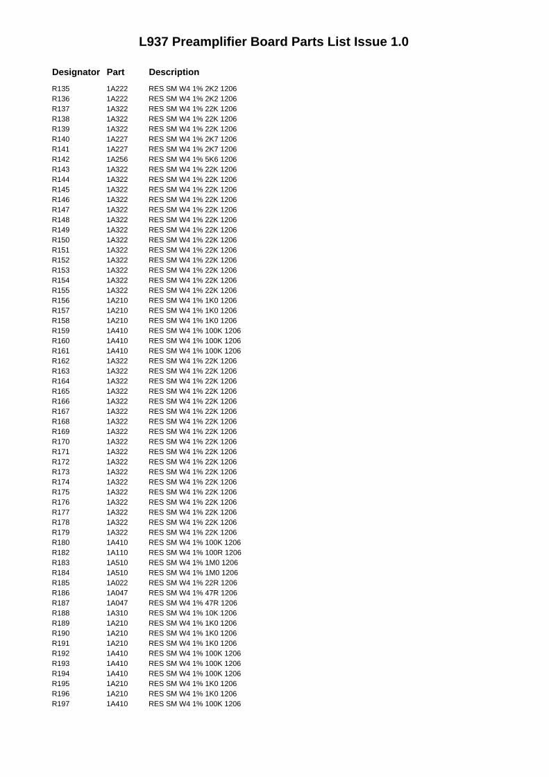
L937 Preamplifier Board Parts List Issue 1.0
Designator Part DescriptionR135 1A222 RES SM W4 1% 2K2 1206R136 1A222 RES SM W4 1% 2K2 1206R137 1A322 RES SM W4 1% 22K 1206R138 1A322 RES SM W4 1% 22K 1206R139 1A322 RES SM W4 1% 22K 1206R140 1A227 RES SM W4 1% 2K7 1206R141 1A227 RES SM W4 1% 2K7 1206R142 1A256 RES SM W4 1% 5K6 1206R143 1A322 RES SM W4 1% 22K 1206R144 1A322 RES SM W4 1% 22K 1206R145 1A322 RES SM W4 1% 22K 1206R146 1A322 RES SM W4 1% 22K 1206R147 1A322 RES SM W4 1% 22K 1206R148 1A322 RES SM W4 1% 22K 1206R149 1A322 RES SM W4 1% 22K 1206R150 1A322 RES SM W4 1% 22K 1206R151 1A322 RES SM W4 1% 22K 1206R152 1A322 RES SM W4 1% 22K 1206R153 1A322 RES SM W4 1% 22K 1206R154 1A322 RES SM W4 1% 22K 1206R155 1A322 RES SM W4 1% 22K 1206R156 1A210 RES SM W4 1% 1K0 1206R157 1A210 RES SM W4 1% 1K0 1206R158 1A210 RES SM W4 1% 1K0 1206R159 1A410 RES SM W4 1% 100K 1206R160 1A410 RES SM W4 1% 100K 1206R161 1A410 RES SM W4 1% 100K 1206R162 1A322 RES SM W4 1% 22K 1206R163 1A322 RES SM W4 1% 22K 1206R164 1A322 RES SM W4 1% 22K 1206R165 1A322 RES SM W4 1% 22K 1206R166 1A322 RES SM W4 1% 22K 1206R167 1A322 RES SM W4 1% 22K 1206R168 1A322 RES SM W4 1% 22K 1206R169 1A322 RES SM W4 1% 22K 1206R170 1A322 RES SM W4 1% 22K 1206R171 1A322 RES SM W4 1% 22K 1206R172 1A322 RES SM W4 1% 22K 1206R173 1A322 RES SM W4 1% 22K 1206R174 1A322 RES SM W4 1% 22K 1206R175 1A322 RES SM W4 1% 22K 1206R176 1A322 RES SM W4 1% 22K 1206R177 1A322 RES SM W4 1% 22K 1206R178 1A322 RES SM W4 1% 22K 1206R179 1A322 RES SM W4 1% 22K 1206R180 1A410 RES SM W4 1% 100K 1206R182 1A110 RES SM W4 1% 100R 1206R183 1A510 RES SM W4 1% 1M0 1206R184 1A510 RES SM W4 1% 1M0 1206R185 1A022 RES SM W4 1% 22R 1206R186 1A047 RES SM W4 1% 47R 1206R187 1A047 RES SM W4 1% 47R 1206R188 1A310 RES SM W4 1% 10K 1206R189 1A210 RES SM W4 1% 1K0 1206R190 1A210 RES SM W4 1% 1K0 1206R191 1A210 RES SM W4 1% 1K0 1206R192 1A410 RES SM W4 1% 100K 1206R193 1A410 RES SM W4 1% 100K 1206R194 1A410 RES SM W4 1% 100K 1206R195 1A210 RES SM W4 1% 1K0 1206R196 1A210 RES SM W4 1% 1K0 1206R197 1A410 RES SM W4 1% 100K 1206
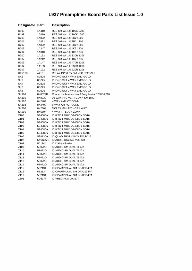
L937 Preamplifier Board Parts List Issue 1.0
Designator Part DescriptionR198 1A410 RES SM W4 1% 100K 1206R199 1A410 RES SM W4 1% 100K 1206R200 1A822 RES SM W4 1% 2R2 1206R201 1A822 RES SM W4 1% 2R2 1206R202 1A822 RES SM W4 1% 2R2 1206R203 1A247 RES SM W4 1% 4K7 1206R204 1A310 RES SM W4 1% 10K 1206R300 1A133 RES SM W4 1% 330R 1206R302 1A212 RES SM W4 1% 1K2 1206R303 1A147 RES SM W4 1% 470R 1206R304 1A133 RES SM W4 1% 330R 1206R307 1A122 RES SM W4 1% 220R 1206RLY100 A216 RELAY DPDT 5V SM NEC EB2-5NUSK2 8D225 PHONO SKT 4-WAY EMC GOLDSK3 8D225 PHONO SKT 4-WAY EMC GOLDSK4 8D225 PHONO SKT 4-WAY EMC GOLDSK5 8D225 PHONO SKT 4-WAY EMC GOLDSK6 8D226 PHONO SKT 2-WAY EMC GOLDSK100 8K8022B Connector 1mm vertical 22way Molex 52806-2210SK101 8K8330 30-WAY FFC VERT CONN SM 1MMSK102 8K2404 4-WAY AMP CT CONNSK103 8K2408 8-WAY AMP CT CONNSK300 8K2304 MOLEX MINI FIT HCS 4 WAYSK301 8K6604 4-WAY FR LOCK CONNZ100 5S408DY IC 8 TO 1 MUX DG408DY SO16Z101 5S408DY IC 8 TO 1 MUX DG408DY SO16Z102 5S408DY IC 8 TO 1 MUX DG408DY SO16Z103 5S408DY IC 8 TO 1 MUX DG408DY SO16Z104 5S408DY IC 8 TO 1 MUX DG408DY SO16Z105 5S408DY IC 8 TO 1 MUX DG408DY SO16Z106 5S413DY IC QUAD SPST CMOS SW SO16Z107 5AVSDVC IC AUDIO DIGITAL VOL SMZ108 5A1844 IC DS1844S-010Z109 5B072D IC AUDIO SM DUAL TL072Z110 5B072D IC AUDIO SM DUAL TL072Z111 5B072D IC AUDIO SM DUAL TL072Z112 5B072D IC AUDIO SM DUAL TL072Z113 5B072D IC AUDIO SM DUAL TL072Z114 5B072D IC AUDIO SM DUAL TL072Z115 5B2134 IC OPAMP DUAL SM OPA2134PAZ116 5B2134 IC OPAMP DUAL SM OPA2134PAZ117 5B2134 IC OPAMP DUAL SM OPA2134PAZ301 5D317T IC VREG POS LM317T
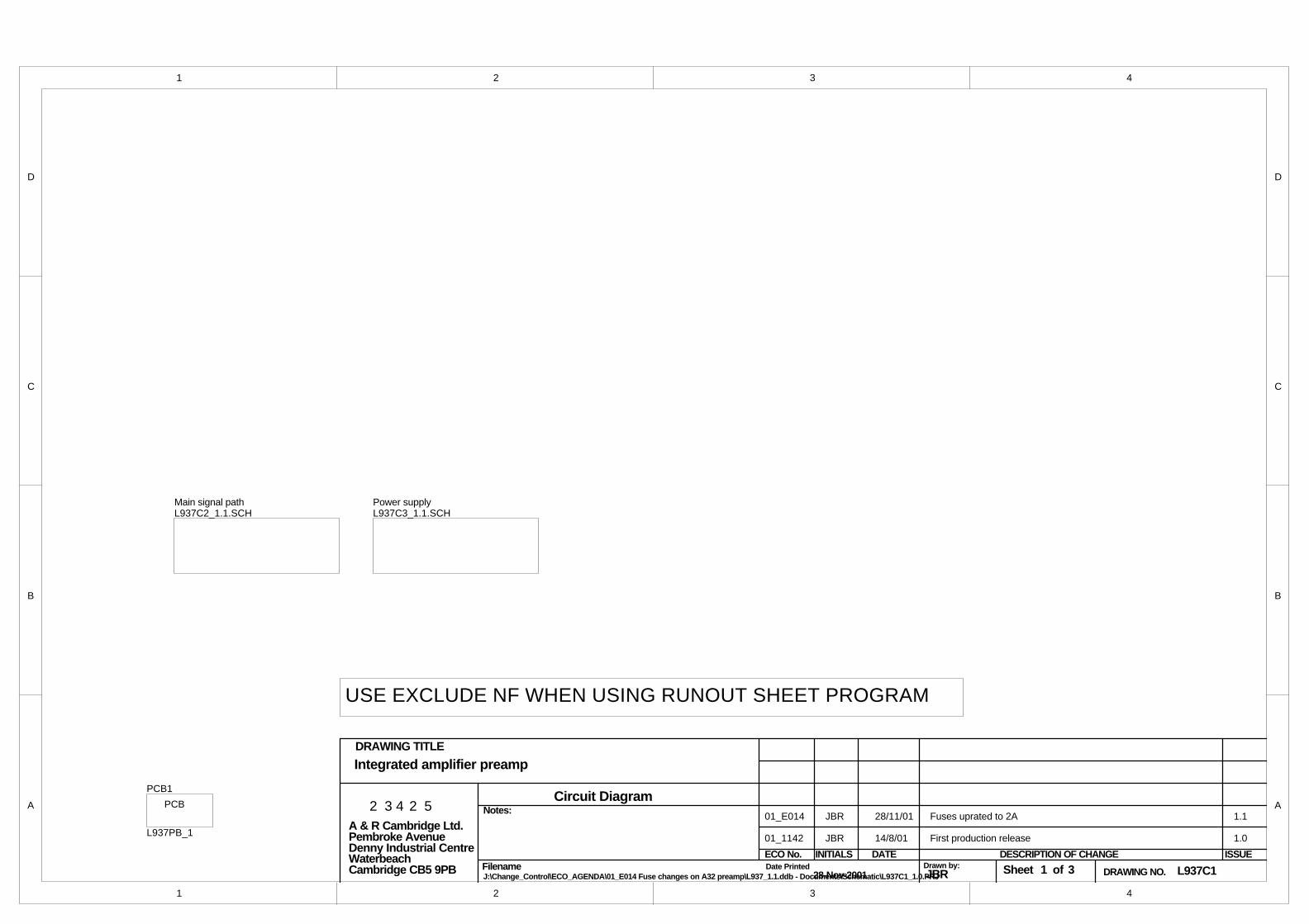
1 2 3 4
A
B
C
D
4321
D
C
B
A
ISSUE
DRAWING NO.
23425
DRAWING TITLE
Drawn by:DATE
FilenameECO No. DESCRIPTION OF CHANGE
J:\Change_Control\ECO_AGENDA\01_E014 Fuse changes on A32 preamp\L937_1.1.ddb - Documents\Schematic\L937C1_1.0.PRJ
A & R Cambridge Ltd.Pembroke AvenueDenny Industrial CentreWaterbeachCambridge CB5 9PB
Integrated amplifier preamp
Circuit Diagram
L937C1JBR28-Nov-2001
INITIALSDate Printed 1 3Sheet of
Notes:
Main signal pathL937C2_1.1.SCH
Power supplyL937C3_1.1.SCH
USE EXCLUDE NF WHEN USING RUNOUT SHEET PROGRAM
PCBPCB1
L937PB_1 01_1142 JBR 14/8/01 First production release 1.0
01_E014 JBR 28/11/01 Fuses uprated to 2A 1.1
1 2 3 4 5 6 7 8
A
B
C
D
87654321
D
C
B
A
ISSUEDRAWING NO.
23425
DRAWING TITLE
Drawn by:DATE
FilenameECO No. DESCRIPTION OF CHANGE
J:\Change_Control\ECO_AGENDA\01_E014 Fuse changes on A32 preamp\L937_1.1.ddb - Documents\Schematic\L937C2_1.0.SCH
A & R Cambridge Ltd.Pembroke AvenueDenny Industrial CentreWaterbeachCambridge CB5 9PB
Integrated amplifier preamp - main signal path
Circuit Diagram
L937C2JBR28-Nov-2001
INITIALSDate Printed 2 3Sheet of
Notes:
EMC
1
N
F
SK2A
PHONO4G
C1001N0 SM
0V_SIG
0V_SIG
R100
1K0 SM
R101
1K0 SM
R103100K SM
R104100K SM
D100BAV99W DUAL SM+15V -15V
0V_SIG
0V_SIG
D101BAV99W DUAL SM
+15V -15V
N
F
SK2B
PHONO4G
0V_SIG
R102
1K0 SM
R125
1K0 SM
R105100K SM
R128100K SM
D102BAV99W DUAL SM+15V -15V
0V_SIG
0V_SIG
D106BAV99W DUAL SM
+15V -15V
EMC
1
N
F
SK3A
PHONO4G
C1211N0 SM
0V_SIG
0V_SIG
R126
1K0 SM
R127
1K0 SM
R129100K SM
R130100K SM
D107BAV99W DUAL SM+15V -15V
0V_SIG
0V_SIG
D108BAV99W DUAL SM
+15V -15V
N
F
SK3B
PHONO4G
0V_SIG
R156
1K0 SM
R157
1K0 SM
R159100K SM
R160100K SM
D112BAV99W DUAL SM+15V -15V
0V_SIG
0V_SIG
D113BAV99W DUAL SM
+15V -15V
EMC
1
N
F
SK4A
PHONO4G
C1391N0 SM
0V_SIG
0V_SIG
R158
1K0 SM
R189
1K0 SM
R161100K SM
R192100K SM
D114BAV99W DUAL SM+15V -15V
0V_SIG
0V_SIG
D115BAV99W DUAL SM
+15V -15V
EMC
1
N
F
SK5A
PHONO4G
0V_SIG
R190
1K0 SM
R191
1K0 SM
R193100K SM
R194100K SM
D116BAV99W DUAL SM+15V -15V
0V_SIG
0V_SIG
D117BAV99W DUAL SM
+15V -15V
CD INPUT
TUNER INPUT
AV INPUT
DVD INPUT
TAPE INPUT
VCR INPUT
C1601N0 SM
0V_SIG
C1641N0 SM
0V_SIG
0V_SIG
R195
1K0 SM
R196
1K0 SM
R197100K SM
R198100K SM
D118BAV99W DUAL SM+15V -15V
0V_SIG
0V_SIG
D119BAV99W DUAL SM
+15V -15V
EMC
1
N
F
SK6
PHONO2G
AUX INPUT
CD L
CD R
TUNER L
TUNER R
AV L
AV R
DVD L
DVD R
TAPE IN L
TAPE IN R
VCR IN L
VCR IN R
AUX L
AUX R
AUX LCD LTUNER LAV LDVD L
VCR IN LMODULE L
0V_SIG
AUX RCD RTUNER RAV RDVD R
VCR IN RMODULE R
0V_SIG
TAPE 0TAPE 1
TAPE 2
TAPE 0TAPE 1
TAPE 2
+15V
+15V-15V
-15V
0V_SIG
0V_SIG
C104100N SM
C105100N SM
+15V
-15V
3
21
Z109ATL072 SM
84
Z113CTL072 SM
R1061M0 SM
0V_SIG
R108
47R SM
D103BAV99W DUAL SM
+15V -15V
N
F
SK4B
PHONO4G
0V_SIG
5
67
Z109BTL072 SM
R1071M0 SM
0V_SIG
R109
47R SM
D104BAV99W DUAL SM
+15V -15V
3
21
Z110ATL072 SM
R1311M0 SM
0V_SIG
R133
47R SM
D109BAV99W DUAL SM
+15V -15V
5
67
Z110BTL072 SM
R1321M0 SM
0V_SIG
R134
47R SM
D110BAV99W DUAL SM
+15V -15V
N
F
SK5B
PHONO4G
0V_SIG
+15V
+15V-15V
-15V
-15V
-15V
C108100P SM
C109100P SM
C129100P SM
C130100P SM
AUX LCD LTUNER LAV LDVD LTAPE IN L
MODULE L
0V_SIG
AUX RCD RTUNER RAV RDVD RTAPE IN R
MODULE R
VCR 0VCR 1
VCR 2
VCR 0VCR 1
VCR 2
0V_SIG
0V_SIG
0V_SIG
TAPE OUTPUT
VCR OUTPUT
C106100N SM
C107100N SM
+15V
-15V0V_SIG
C125100N SM
C126100N SM
+15V
-15V
0V_SIG
C127100N SM
C128100N SM
+15V
-15V
0V_SIG
AUX LCD LTUNER LAV LDVD LTAPE IN LVCR IN LMODULE L
AUX RCD RTUNER RAV RDVD RTAPE IN RVCR IN RMODULE R
LISTEN 0LISTEN 1LISTEN 2
LISTEN 0LISTEN 1LISTEN 2
0V_SIG
0V_SIG
C143100N SM
C144100N SM
+15V
-15V
0V_SIG
C145100N SM
C146100N SM
+15V
-15V
0V_SIG
84
Z114CTL072 SM
R17022K SMR16222K SM R17122K SMR16322K SM R17222K SMR16422K SM R17322K SMR16522K SM
R17422K SMR16622K SM R17522K SMR16722K SM R17622K SMR16822K SM R17722K SMR16922K SM
+15V
+15VR178
22K SM
C148
22P SM
R179
22K SM
C149
22P SM
5
67 Z115B
OPA2134PA SM
5
67 Z116B
OPA2134PA SM
84
Z116C
OPA
2134
PA S
M
0V_SIG
0V_SIG
R183
1M0 SM
R184
1M0 SMR199
100K SM
R180
100K SM
0V_SIG
0V_SIG
+5V
+5V
+5V
+5V
+5V
+5V
X04X15X26X37X412X511X610
X79
EN2A01A116A215
V-3
D 8
GND14
V+ 13Z100
DG408DY
X04X15X26X37X412
X511X610X79
EN2A01A116A215
V-3
D 8
GND14
V+ 13Z101
DG408DY
X04X15X26
X37X412X511X610X79
EN2A01A116A215
V-3
D 8
GND14
V+ 13Z102
DG408DY
X04
X15X26X37X412X511X610X79
EN2A01A116A215
V-3
D 8
GND14
V+ 13Z103
DG408DY
X04X15X26X37X412X511X610X79
EN2A01A116
A215
V-3
D 8
GND14
V+ 13Z104
DG408DY
X04X15X26X37X412X511X610X79
EN2
A01A116A215
V-3
D 8
GND14
V+ 13Z105
DG408DY
LIN4
LGND5
RGND12
RIN13
LMO 2
RMO 15
AVC
C1
DVC
C7
LFO 3
RFO 14
DG
ND
11
XCS
6D
ATA
9C
CLK
10
XMU
TE8
AGN
D16
Z107VSDVC
0V_SIG
C186
100N SM
+5V
+C15410U EL
C155100N SM C156
100N SM
0V_SIG0V_SIG
+5V
SCLK
SDAT
ASL
OAD
0V_SIG
0V_SIG
R200
2R2 SMR201
2R2 SMR202
2R2 SM0V_SCLK
0V_SLOAD
0V_SDATA
C15822P SM
C15922P SM
0V_SIG
0V_SIG
SEL11
S2 14D12
V+ 13S13
S3 11
V-4
GND5 VL 12
S46
D3 10D47
SEL3 9
D2 15
SEL48
SEL2 16Z106
DG413DY
+15V-15V
0V_SIG
+5V
TONE*
TONE*
TONE*
TONE*
C152100N SM
0V_SIG
C153100N SM
R186
47R SM
R187
47R SM
R185
22R SM + C157100U EL
R1102K2 SM
R1112K2 SM
+ C110100U EL
R112
22K SM
0V_SIG
R11322K SM
+ C11110U CERAFINE
+5V
3
21
Z111ATL072 SM
5
67
Z112BTL072 SM3
21
Z112ATL072 SM
5
67
Z111BTL072 SM
84
Z109CTL072 SM
84
Z110CTL072 SM
+
C117
10U CERAFINE
R12122K SM
R11922K SM
R12022K SM
+ C11610U CERAFINE
0V_SIG
D105BAV99W DUAL SM
0V_SIG
R114
22K SM
R118
22K SM
1618
17Z108D
DS
1844
1519
14Z108A
DS
1844
R1152K7 SM
R1162K7 SM
0V_SIG
R1175K6 SM
R1352K2 SM
R1362K2 SM
+ C131100U EL
R137
22K SM
0V_SIG
R13822K SM
+ C13210U CERAFINE
+5V
3
21
Z113ATL072 SM
5
67
Z114BTL072 SM3
21
Z114ATL072 SM
5
67
Z113BTL072 SM
+
C138
10U CERAFINE
R14622K SM
R14422K SM
R14522K SM
+ C13710U CERAFINE
0V_SIG
D111BAV99W DUAL SM
0V_SIGR139
22K SM
R143
22K SM
62
7Z108B
DS
1844
53
4Z108C
DS
1844
R1402K7 SM
R1412K7 SM
0V_SIG
R1425K6 SM
84
Z111CTL072 SM
84
Z112CTL072 SM
+15V
+15V-15V
-15V
C169100N SM
C168100N SM
C172100N SM
C173100N SM
C176100N SM
C177100N SM
C180100N SM
C181100N SM
0V_SIG 0V_SIG 0V_SIG 0V_SIG
C170100N SM
C171100N SM
C174100N SM
C175100N SM
C178100N SM
C179100N SM
C182100N SM
C183100N SM
C184100N SM
C185100N SM
0V_SIG 0V_SIG 0V_SIG 0V_SIG 0V_SIG
PS 1R/W 8
DOUT 11RST9 DIN12 CLK13 VCC
20G
ND
10
Z108E
IC DS1844
+5V
SDATASCLK
TONEID
C118100N SM
+ C12010U EL
0V_SIG
C11910N SM
R122
2R2 SM0V_TONEID
C115
22P SM
C136
22P SM
0V_SDATA
0V_SCLK
R124
2R2 SM
R123
2R2 SM
R15122K SMR14722K SM R15222K SMR14822K SM R15322K SMR14922K SM R15422K SMR15022K SM R15522K SM
LISTEN 0LISTEN 1LISTEN 2VCR 0VCR 1VCR 2TAPE 0TAPE 1TAPE 2
TONE*
0V_TONEID
TONEID
0V_SDATA
SDATA
0V_SLOAD
SLOAD
0V_SCLK
SCLK
1234
SK102
AMPCT4
0V_SIG
12345678
SK103
AMPCT8
+15V
0V_SIG
-15V
AUX R
AUX L
TO P
HO
NO
PC
B
TO POWER AMP I/P
TO M
ICR
O /
DIS
PLAY
PC
B
3
21Z115A
OPA2134PA SM
3
21Z116A
OPA2134PA SM
3
21Z117A
OPA2134PA SM
5
67Z117B
OPA2134PA SM
84
Z115C
OPA
2134
PA S
M 84
Z117C
OPA
2134
PA S
M
RLY100A
RLY DPDT 5V SM
RLY100B
RLY DPDT 5V SM
+
-
RLY100CRLY DPDT 5V SM
D120BAS16W SM
Q100BC849B R203
4K7 SMMUTE*
0V_D
+5V
MUTE*
0V_D
+ C18710U EL
123456789
101112131415161718192021222324252627282930
SK101
FFC30V SM
0V_MODULE
AUX L
AUX R
CD L
CD R
TUNER L
TUNER R
AV L
AV R
DVD L
DVD R
TAPE IN L
TAPE IN R
VCR IN L
VCR IN R
MODULE LMODULE R
TO P
LUG
IN M
OD
ULE
PC
B
+5V
R188
10K SM0V_SIG
0V_HF
D121BAV99W DUAL SM
D122BAV99W DUAL SM+15V -15V
C113470N PE
C134470N PE
C150
470N PE
C151
470N PE
+ C18810U EL
+ C18910U EL
+15V
-15V
0V_SIG
+ C19010U EL
+ C19110U EL
+15V
-15V
0V_SIG
R20410K SM
C112
470N PEC192
470N PE
C133
470N PEC193
470N PE
C101470P FKP2
C102470P FKP2
C103470P FKP2
C122470P FKP2
C123470P FKP2
C124470P FKP2
C140470P FKP2
C141470P FKP2
C142470P FKP2
C161470P FKP2
C162470P FKP2
C163470P FKP2
C165470P FKP2
C166470P FKP2
C114CFKP2 63V 2N2
C135CFKP2 63V 2N2
CDL1 CDL
CDR
CDR1
TUNL1
TUNR1
TUNL
TUNR
AVL1
AVR1
AVL
AVR
DVDL1
DVDR1
DVDL
DVDR
TAPEIL1
TAPEIR1
TAPEIL
TAPEIR
VCRIL1
VCRIR1
VCRIL
VCRIR
AUXL
AUXR
+15V1
-15V1
AUXL1
AUXR1
LISTEN2LISTEN1
LISTEN0
LIST2LIST1
LIST0
VCR2VCR1
VCR0
VCR21VCR11
VCR01
TAPE2TAPE1
TAPE0
TAP2TAP1
TAP0
TAPEO1
TAPE02
VCRO1
VCR02
Z115_1A
Z116_1A
/TONE
Z107_4
Z107_13
Z107_1
SK102_1
SK102_3
Z116_1B
Z113_3
Z111_3
Z115_1B
Z111_1
Z111_7
Z108_19
Z112_3Z112_1
Z112_7
TONEIDSDATA
SCLK
Z106_11Z114_7Z114_1Z114_3
Z108_3
Z113_7
Z113_1
AUXIL1
AUXIR1
Z106_14
+15V2
-15V2
R182100R SM
123456789
10111213141516171819202122
SK100
FFC22V1MM
C147100N PE
C167100N PE
01_1142 JBR 14/8/01 First production release 1.0
R18110K SM
01_E014 JBR 28/11/01 Fuses uprated to 2A 1.1
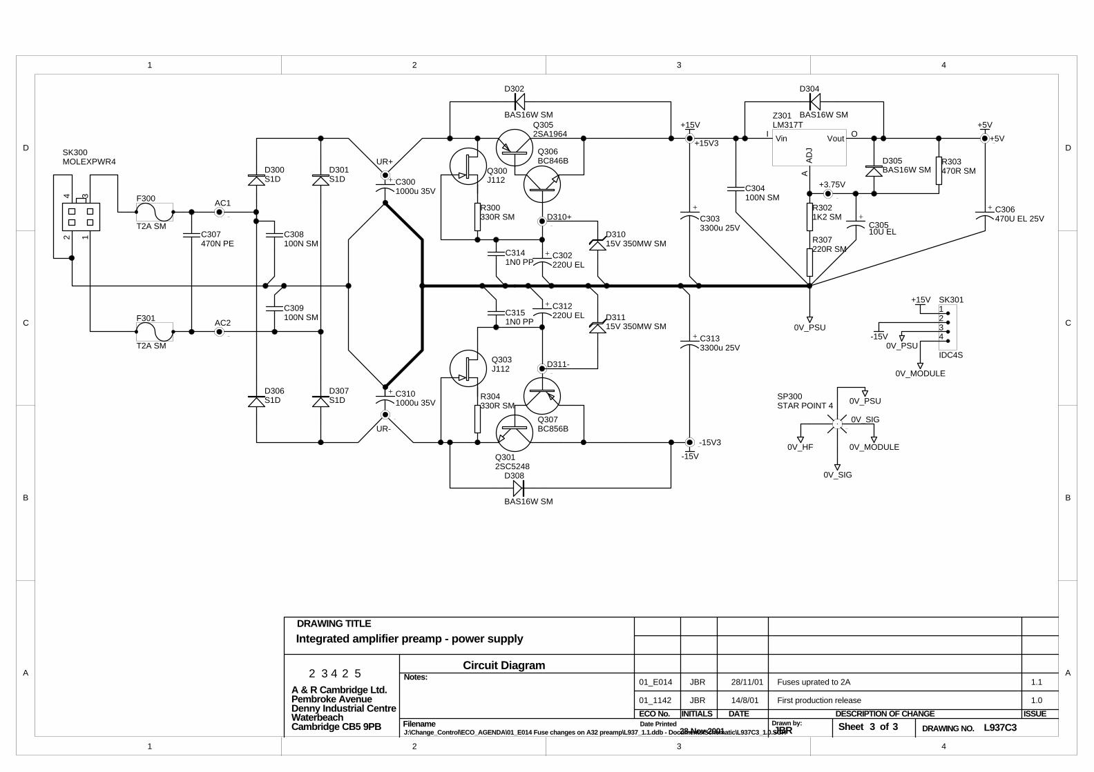
1 2 3 4
A
B
C
D
4321
D
C
B
A
ISSUE
DRAWING NO.
23425
DRAWING TITLE
Drawn by:DATE
FilenameECO No. DESCRIPTION OF CHANGE
J:\Change_Control\ECO_AGENDA\01_E014 Fuse changes on A32 preamp\L937_1.1.ddb - Documents\Schematic\L937C3_1.0.SCH
A & R Cambridge Ltd.Pembroke AvenueDenny Industrial CentreWaterbeachCambridge CB5 9PB
Integrated amplifier preamp - power supply
Circuit Diagram
L937C3JBR28-Nov-2001
INITIALSDate Printed 3 3Sheet of
Notes:
12
34
SK300MOLEXPWR4
+ C3001000u 35V
+ C3101000u 35V
D302
BAS16W SM
D308
BAS16W SM
VinI
ADJ
A
Vout O
Z301LM317T
D305BAS16W SM
D304
BAS16W SM
R303470R SM
+C30510U EL
C304100N SM
R3021K2 SM
R307220R SM
+15V
-15V
+5V
0V_PSU
SP300STAR POINT 4 0V_PSU
0V_SIG
0V_HF 0V_MODULE
+ C306470U EL 25V
C307470N PE
C308100N SM
C309100N SM
Q3012SC5248
Q3052SA1964
+ C302220U EL
+ C312220U EL
Q300J112
Q303J112
R300330R SM
R304330R SM
+C3033300u 25V
+ C3133300u 25V
D31015V 350MW SM
D31115V 350MW SM
Q306BC846B
Q307BC856B
1234
SK301
IDC4S
+15V
-15V0V_PSU
0V_MODULE
AC1
AC2
UR+
UR-
D311-
D310+
+15V3 +5V
+3.75V
0V_SIG
-15V3
C3141N0 PP
C3151N0 PP
D300S1D
D301S1D
D306S1D
D307S1D
01_1142 JBR 14/8/01 First production release 1.0
01_E014 JBR 28/11/01 Fuses uprated to 2A 1.1
F300
T2A SM
F301
T2A SM
3rd Channel Board L911
Contents
! Component overlay
! Parts list
! Circuit diagrams
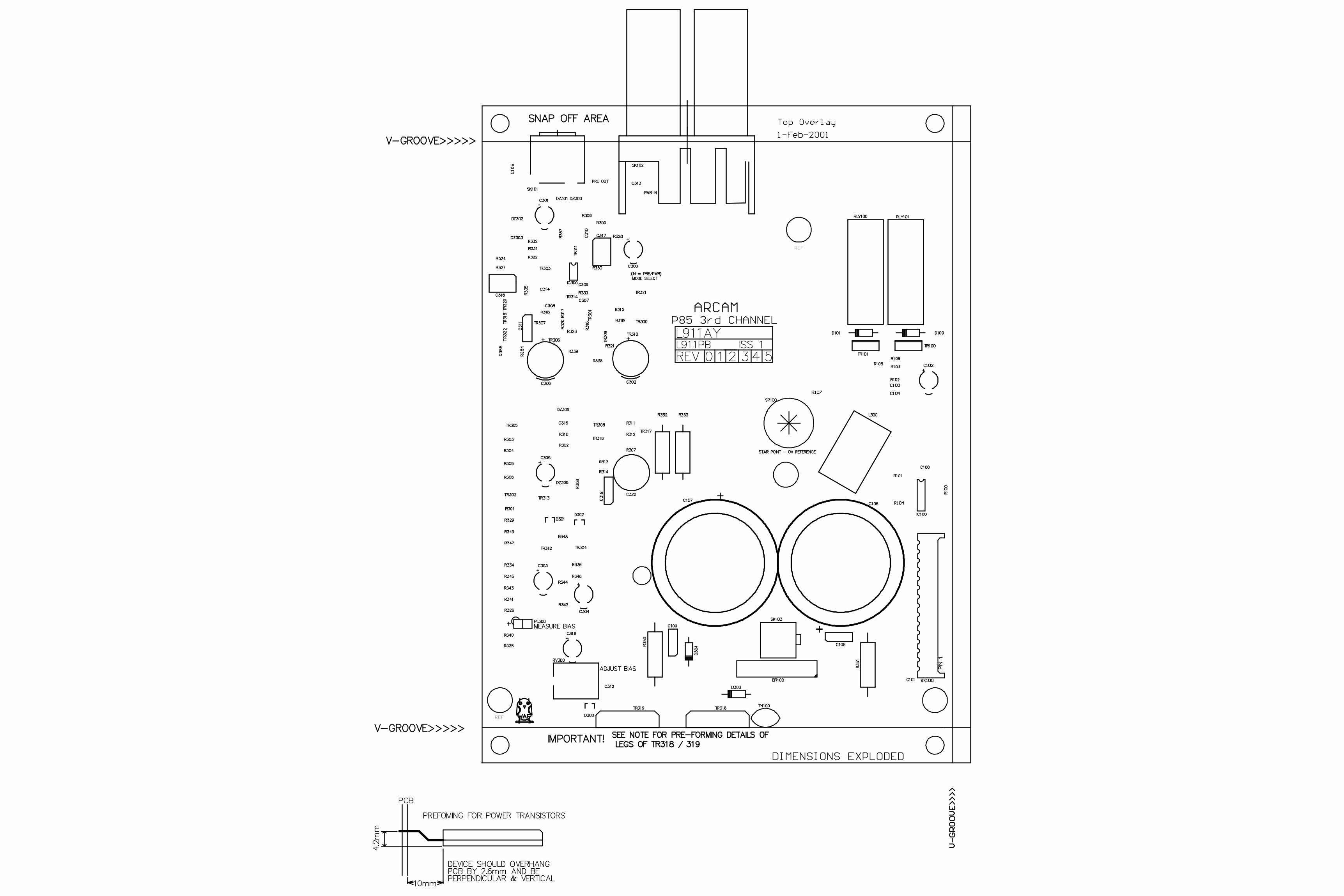
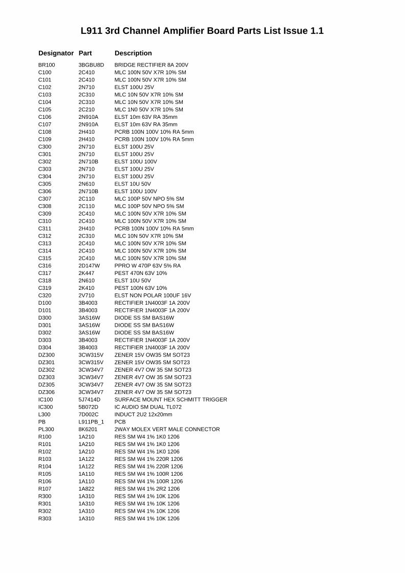
L911 3rd Channel Amplifier Board Parts List Issue 1.1
Designator Part DescriptionBR100 3BGBU8D BRIDGE RECTIFIER 8A 200VC100 2C410 MLC 100N 50V X7R 10% SMC101 2C410 MLC 100N 50V X7R 10% SMC102 2N710 ELST 100U 25VC103 2C310 MLC 10N 50V X7R 10% SMC104 2C310 MLC 10N 50V X7R 10% SMC105 2C210 MLC 1N0 50V X7R 10% SMC106 2N910A ELST 10m 63V RA 35mmC107 2N910A ELST 10m 63V RA 35mmC108 2H410 PCRB 100N 100V 10% RA 5mmC109 2H410 PCRB 100N 100V 10% RA 5mmC300 2N710 ELST 100U 25VC301 2N710 ELST 100U 25VC302 2N710B ELST 100U 100VC303 2N710 ELST 100U 25VC304 2N710 ELST 100U 25VC305 2N610 ELST 10U 50VC306 2N710B ELST 100U 100VC307 2C110 MLC 100P 50V NPO 5% SMC308 2C110 MLC 100P 50V NPO 5% SMC309 2C410 MLC 100N 50V X7R 10% SMC310 2C410 MLC 100N 50V X7R 10% SMC311 2H410 PCRB 100N 100V 10% RA 5mmC312 2C310 MLC 10N 50V X7R 10% SMC313 2C410 MLC 100N 50V X7R 10% SMC314 2C410 MLC 100N 50V X7R 10% SMC315 2C410 MLC 100N 50V X7R 10% SMC316 2D147W PPRO W 470P 63V 5% RAC317 2K447 PEST 470N 63V 10%C318 2N610 ELST 10U 50VC319 2K410 PEST 100N 63V 10%C320 2V710 ELST NON POLAR 100UF 16VD100 3B4003 RECTIFIER 1N4003F 1A 200VD101 3B4003 RECTIFIER 1N4003F 1A 200VD300 3AS16W DIODE SS SM BAS16WD301 3AS16W DIODE SS SM BAS16WD302 3AS16W DIODE SS SM BAS16WD303 3B4003 RECTIFIER 1N4003F 1A 200VD304 3B4003 RECTIFIER 1N4003F 1A 200VDZ300 3CW315V ZENER 15V OW35 SM SOT23DZ301 3CW315V ZENER 15V OW35 SM SOT23DZ302 3CW34V7 ZENER 4V7 OW 35 SM SOT23DZ303 3CW34V7 ZENER 4V7 OW 35 SM SOT23DZ305 3CW34V7 ZENER 4V7 OW 35 SM SOT23DZ306 3CW34V7 ZENER 4V7 OW 35 SM SOT23IC100 5J7414D SURFACE MOUNT HEX SCHMITT TRIGGERIC300 5B072D IC AUDIO SM DUAL TL072L300 7D002C INDUCT 2U2 12x20mmPB L911PB_1 PCBPL300 8K6201 2WAY MOLEX VERT MALE CONNECTORR100 1A210 RES SM W4 1% 1K0 1206R101 1A210 RES SM W4 1% 1K0 1206R102 1A210 RES SM W4 1% 1K0 1206R103 1A122 RES SM W4 1% 220R 1206R104 1A122 RES SM W4 1% 220R 1206R105 1A110 RES SM W4 1% 100R 1206R106 1A110 RES SM W4 1% 100R 1206R107 1A822 RES SM W4 1% 2R2 1206R300 1A310 RES SM W4 1% 10K 1206R301 1A310 RES SM W4 1% 10K 1206R302 1A310 RES SM W4 1% 10K 1206R303 1A310 RES SM W4 1% 10K 1206
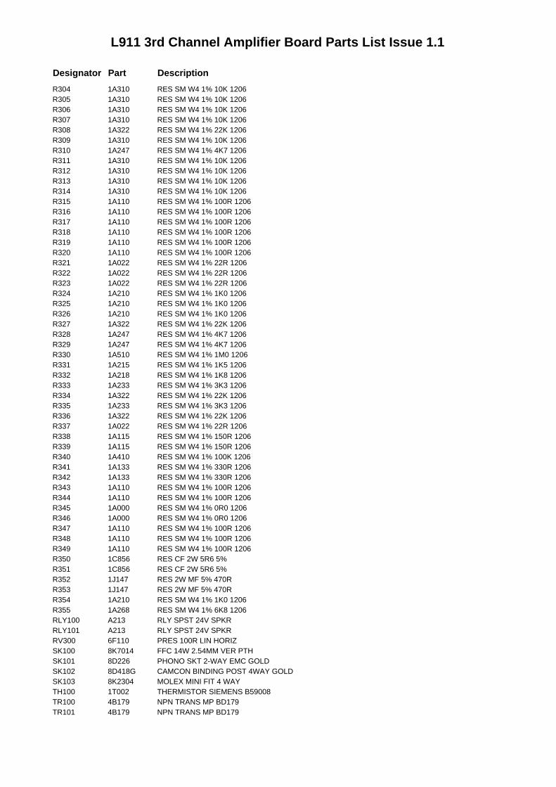
L911 3rd Channel Amplifier Board Parts List Issue 1.1
Designator Part DescriptionR304 1A310 RES SM W4 1% 10K 1206R305 1A310 RES SM W4 1% 10K 1206R306 1A310 RES SM W4 1% 10K 1206R307 1A310 RES SM W4 1% 10K 1206R308 1A322 RES SM W4 1% 22K 1206R309 1A310 RES SM W4 1% 10K 1206R310 1A247 RES SM W4 1% 4K7 1206R311 1A310 RES SM W4 1% 10K 1206R312 1A310 RES SM W4 1% 10K 1206R313 1A310 RES SM W4 1% 10K 1206R314 1A310 RES SM W4 1% 10K 1206R315 1A110 RES SM W4 1% 100R 1206R316 1A110 RES SM W4 1% 100R 1206R317 1A110 RES SM W4 1% 100R 1206R318 1A110 RES SM W4 1% 100R 1206R319 1A110 RES SM W4 1% 100R 1206R320 1A110 RES SM W4 1% 100R 1206R321 1A022 RES SM W4 1% 22R 1206R322 1A022 RES SM W4 1% 22R 1206R323 1A022 RES SM W4 1% 22R 1206R324 1A210 RES SM W4 1% 1K0 1206R325 1A210 RES SM W4 1% 1K0 1206R326 1A210 RES SM W4 1% 1K0 1206R327 1A322 RES SM W4 1% 22K 1206R328 1A247 RES SM W4 1% 4K7 1206R329 1A247 RES SM W4 1% 4K7 1206R330 1A510 RES SM W4 1% 1M0 1206R331 1A215 RES SM W4 1% 1K5 1206R332 1A218 RES SM W4 1% 1K8 1206R333 1A233 RES SM W4 1% 3K3 1206R334 1A322 RES SM W4 1% 22K 1206R335 1A233 RES SM W4 1% 3K3 1206R336 1A322 RES SM W4 1% 22K 1206R337 1A022 RES SM W4 1% 22R 1206R338 1A115 RES SM W4 1% 150R 1206R339 1A115 RES SM W4 1% 150R 1206R340 1A410 RES SM W4 1% 100K 1206R341 1A133 RES SM W4 1% 330R 1206R342 1A133 RES SM W4 1% 330R 1206R343 1A110 RES SM W4 1% 100R 1206R344 1A110 RES SM W4 1% 100R 1206R345 1A000 RES SM W4 1% 0R0 1206R346 1A000 RES SM W4 1% 0R0 1206R347 1A110 RES SM W4 1% 100R 1206R348 1A110 RES SM W4 1% 100R 1206R349 1A110 RES SM W4 1% 100R 1206R350 1C856 RES CF 2W 5R6 5%R351 1C856 RES CF 2W 5R6 5%R352 1J147 RES 2W MF 5% 470RR353 1J147 RES 2W MF 5% 470RR354 1A210 RES SM W4 1% 1K0 1206R355 1A268 RES SM W4 1% 6K8 1206RLY100 A213 RLY SPST 24V SPKRRLY101 A213 RLY SPST 24V SPKRRV300 6F110 PRES 100R LIN HORIZSK100 8K7014 FFC 14W 2.54MM VER PTHSK101 8D226 PHONO SKT 2-WAY EMC GOLDSK102 8D418G CAMCON BINDING POST 4WAY GOLDSK103 8K2304 MOLEX MINI FIT 4 WAYTH100 1T002 THERMISTOR SIEMENS B59008TR100 4B179 NPN TRANS MP BD179TR101 4B179 NPN TRANS MP BD179
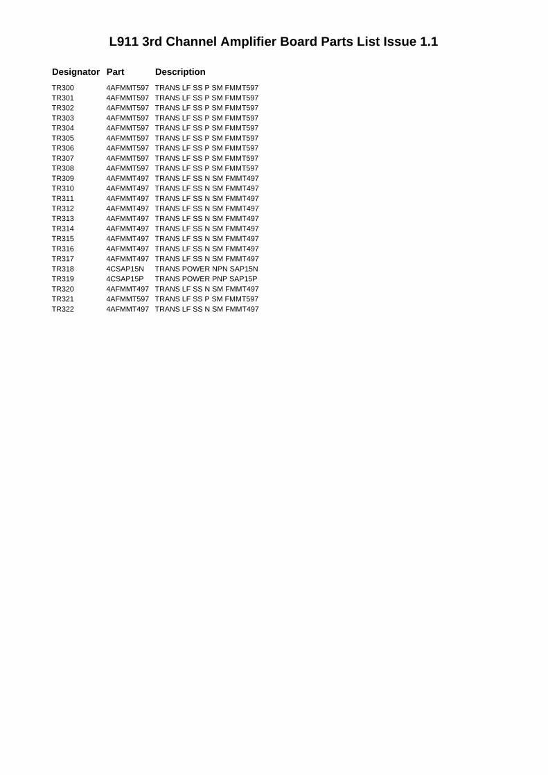
L911 3rd Channel Amplifier Board Parts List Issue 1.1
Designator Part DescriptionTR300 4AFMMT597 TRANS LF SS P SM FMMT597TR301 4AFMMT597 TRANS LF SS P SM FMMT597TR302 4AFMMT597 TRANS LF SS P SM FMMT597TR303 4AFMMT597 TRANS LF SS P SM FMMT597TR304 4AFMMT597 TRANS LF SS P SM FMMT597TR305 4AFMMT597 TRANS LF SS P SM FMMT597TR306 4AFMMT597 TRANS LF SS P SM FMMT597TR307 4AFMMT597 TRANS LF SS P SM FMMT597TR308 4AFMMT597 TRANS LF SS P SM FMMT597TR309 4AFMMT497 TRANS LF SS N SM FMMT497TR310 4AFMMT497 TRANS LF SS N SM FMMT497TR311 4AFMMT497 TRANS LF SS N SM FMMT497TR312 4AFMMT497 TRANS LF SS N SM FMMT497TR313 4AFMMT497 TRANS LF SS N SM FMMT497TR314 4AFMMT497 TRANS LF SS N SM FMMT497TR315 4AFMMT497 TRANS LF SS N SM FMMT497TR316 4AFMMT497 TRANS LF SS N SM FMMT497TR317 4AFMMT497 TRANS LF SS N SM FMMT497TR318 4CSAP15N TRANS POWER NPN SAP15NTR319 4CSAP15P TRANS POWER PNP SAP15PTR320 4AFMMT497 TRANS LF SS N SM FMMT497TR321 4AFMMT597 TRANS LF SS P SM FMMT597TR322 4AFMMT497 TRANS LF SS N SM FMMT497
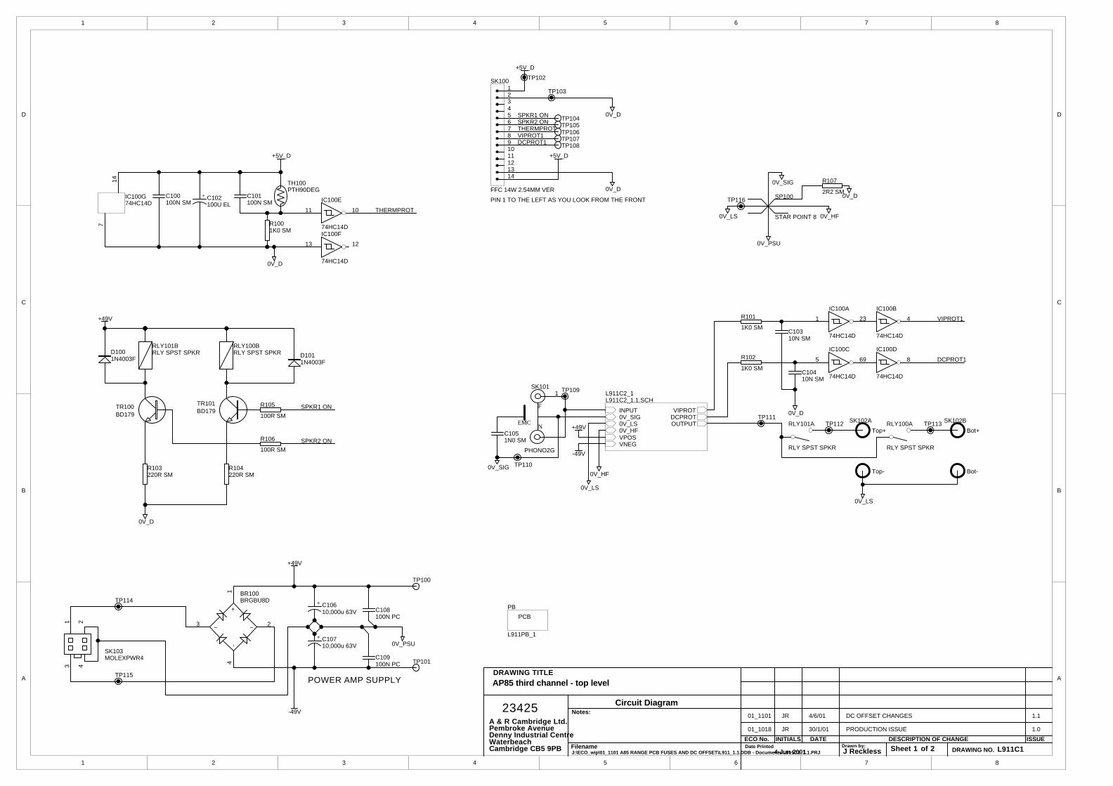
1 2 3 4 5 6 7 8
A
B
C
D
87654321
D
C
B
A
ISSUEDRAWING NO.
23425
DRAWING TITLE
Drawn by:DATE
FilenameECO No. DESCRIPTION OF CHANGE
J:\ECO_wip\01_1101 A85 RANGE PCB FUSES AND DC OFFSET\L911_1.1.DDB - Documents\L911C1_1.1.PRJ
A & R Cambridge Ltd.Pembroke AvenueDenny Industrial CentreWaterbeachCambridge CB5 9PB
AP85 third channel - top level
Circuit Diagram
L911C1J Reckless4-Jun-2001
INITIALSDate Printed 1 2Sheet of
Notes:
+1
~ 2
-4
~3
BR100BRGBU8D
0V_PSU
+49V
-49V
TH100PTH90DEG
+5V_D
0V_D
1011IC100E
74HC14D
5 6IC100C
74HC14D
89IC100D
74HC14D
14
7
IC100G74HC14D
C100100N SM
C101100N SM
R1001K0 SM
POWER AMP SUPPLY
TP100
TP101
+ C10610,000u 63V
+ C10710,000u 63V
C108100N PC
C109100N PC
D1001N4003F D101
1N4003F
SPKR1 ON
SPKR2 ON
TR100BD179
TR101BD179
R105
100R SM
R106
100R SM
R103220R SM
R104220R SM
Top+
Top-
SK102A Bot+
Bot-
SK102BINPUT0V_SIG
VIPROTDCPROTOUTPUT0V_LS
0V_HFVPOSVNEG
L911C2_1L911C2_1.1.SCH
EMC
1
N
F
SK101
PHONO2G
C1051N0 SM
0V_SIG
+49V
-49V
0V_HF
0V_LS
0V_LS
RLY101A
RLY SPST SPKR
RLY101BRLY SPST SPKR
RLY100A
RLY SPST SPKR
RLY100BRLY SPST SPKR
0V_D
1 2IC100A
74HC14D
3 4IC100B
74HC14DC10310N SM
C10410N SM
R101
1K0 SM
R102
1K0 SM
1 2
3 4
SK103MOLEXPWR4
THERMPROT
VIPROT1
DCPROT1
+49V
0V_D
1213IC100F
74HC14D
1234567891011121314
SK100
FFC 14W 2.54MM VER
+5V_D
0V_DSPKR1 ONSPKR2 ONTHERMPROTVIPROT1DCPROT1
0V_D
+5V_D
+ C102100U EL
SP100
STAR POINT 8
0V_PSU
0V_SIG
0V_LS 0V_HF
0V_DPIN 1 TO THE LEFT AS YOU LOOK FROM THE FRONT
R107
2R2 SM
TP102
TP103
TP104TP105TP106TP107TP108
TP109
TP110
TP114
TP115
TP111TP112 TP113
TP116
JR 30/1/01 PRODUCTION ISSUE 1.0
PCBPB
L911PB_1
01_1018
01_1101 JR 4/6/01 DC OFFSET CHANGES 1.1
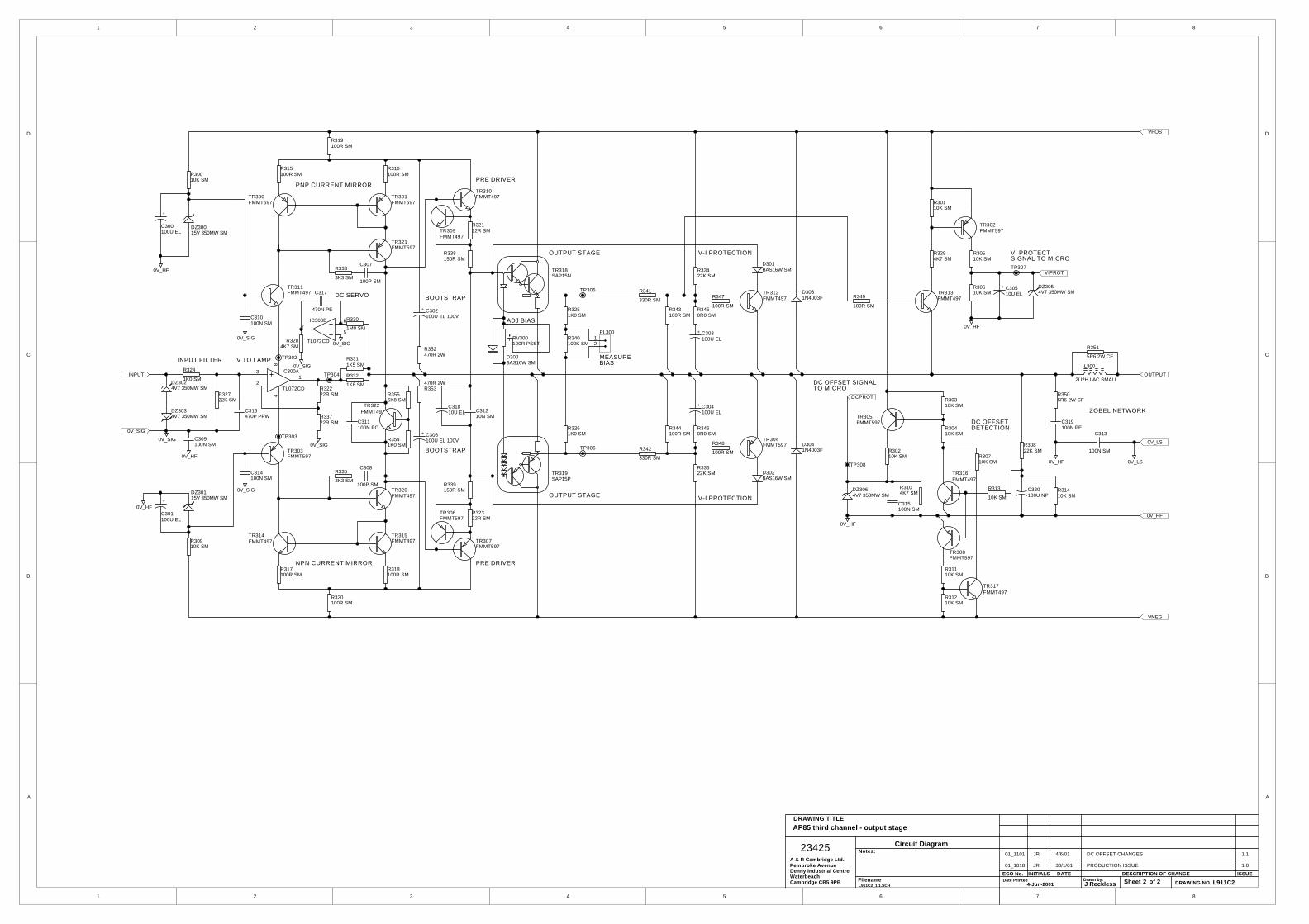
1 2 3 4 5 6 7 8
A
B
C
D
87654321
D
C
B
A
ISSUEDRAWING NO.
23425
DRAWING TITLE
Drawn by:DATE
FilenameECO No. DESCRIPTION OF CHANGE
L911C2_1.1.SCH
A & R Cambridge Ltd.Pembroke AvenueDenny Industrial CentreWaterbeachCambridge CB5 9PB
AP85 third channel - output stage
Circuit Diagram
L911C2J Reckless4-Jun-2001
INITIALSDate Printed 2 2Sheet of
Notes:
R324
1K0 SM
TR300FMMT597
TR301FMMT597
R315100R SM
R316100R SM
R319100R SM
TR314FMMT497
TR315FMMT497
R317100R SM
R318100R SM
R320100R SM
R32222R SM
0V_SIG
C317
470N PE
0V_SIG
0V_SIG
INPUT
0V_SIG
R3505R6 2W CF
C319100N PE
0V_HF 0V_LS
C313
100N SM
R341
330R SM
R342
330R SM
R343100R SM
R344100R SM
R3450R0 SM
R3460R0 SM
R33422K SM
R33622K SM
D301BAS16W SM
D302BAS16W SM
TR312FMMT497
TR304FMMT597
TR313FMMT497
TR302FMMT597
DZ3054V7 350MW SM
0V_HF
VIPROT
C320100U NP
TR305FMMT597
DZ3064V7 350MW SM
0V_HF
DCPROT
OUTPUT
0V_LS
0V_HF
VPOS
VNEG
0V_HF
0V_HF
DZ30015V 350MW SM
DZ30115V 350MW SM
C309100N SM
C310100N SM
C314100N SM
0V_SIG
0V_SIG
D3041N4003F
D3031N4003F
R30210K SM
R32722K SM
RV300100R PSET
C31210N SM
12
PL300
BIAS
R3251K0 SM
R3261K0 SM
ADJ BIAS
D300BAS16W SM
R30010K SM
R30910K SM
R30510K SM
R30610K SM
+ C30510U EL
MEASURE
TR318SAP15N
TR319SAP15P
R30110K SM
C315100N SM
R347
100R SM
R349
100R SM
R348
100R SM
R340100K SM
DZ3024V7 350MW SM
DZ3034V7 350MW SM
3
21
84
IC300A
TL072CD
5
67
IC300B
TL072CDR3284K7 SM
0V_HF
0V_SIG
TR311FMMT497
TR303FMMT597
TR310FMMT497
TR307FMMT597
INPUT FILTER V TO I AMP
DC SERVO
PNP CURRENT MIRROR
NPN CURRENT MIRROR
PRE DRIVER
PRE DRIVER
OUTPUT STAGE
OUTPUT STAGE
V-I PROTECTION
V-I PROTECTION
VI PROTECTSIGNAL TO MICRO
DC OFFSETDETECTION
DC OFFSET SIGNALTO MICRO
ZOBEL NETWORK
TR316FMMT497
TR308FMMT597
TR317FMMT497
R31110K SM
R31210K SM
R313
10K SM
R30310K SM
R30410K SM
R30710K SM
R3104K7 SM
R3294K7 SM
+
C300100U EL
+
C301100U EL
R338150R SM
R339150R SM
R30822K SM
R31410K SM
TR309FMMT497
TR306FMMT597
R32322R SM
R32122R SM
TP302
TP303
TP304
TP307
TP308
TP305
TP306
R33722R SM
R3311K5 SM
R332
1K8 SM
R330
1M0 SM
R333
3K3 SM
R335
3K3 SM
L300
2U2H LAC SMALL
C316470P PPW
C311100N PC
+ C31810U EL
TR321FMMT597
TR320FMMT497
+ C302100U EL 100V
+ C306100U EL 100V
R352470R 2W
R353470R 2W
BOOTSTRAP
BOOTSTRAP
R351
5R6 2W CF
C307
100P SM
C308
100P SM
+ C303100U EL
+ C304100U EL
R3541K0 SM
R3556K8 SM
TR322FMMT497
JR 30/1/01 PRODUCTION ISSUE 1.001_1018
01_1101 JR 4/6/01 DC OFFSET CHANGES 1.1
Transformer Specifications
Contents
! L914TX
! L915TX
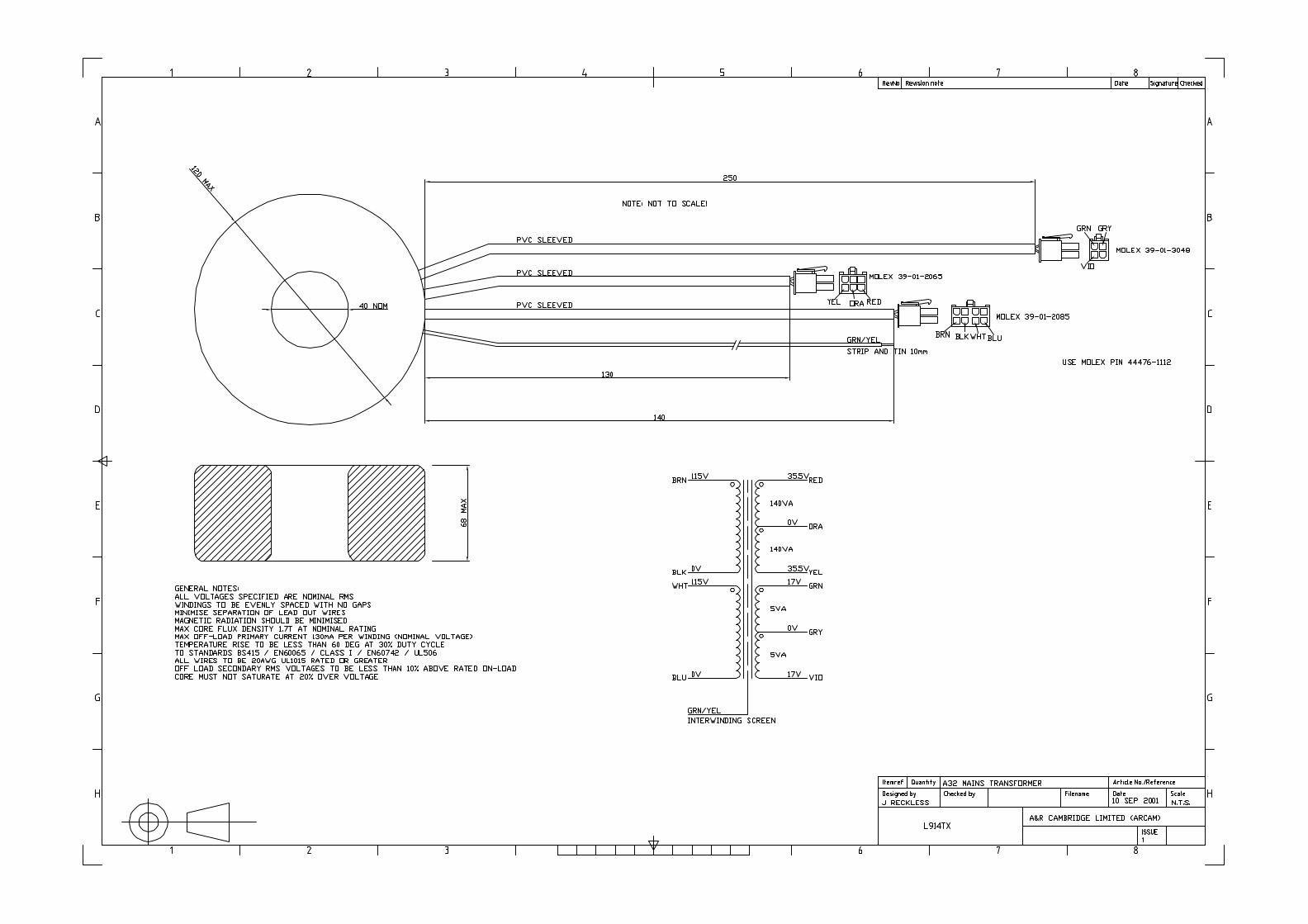
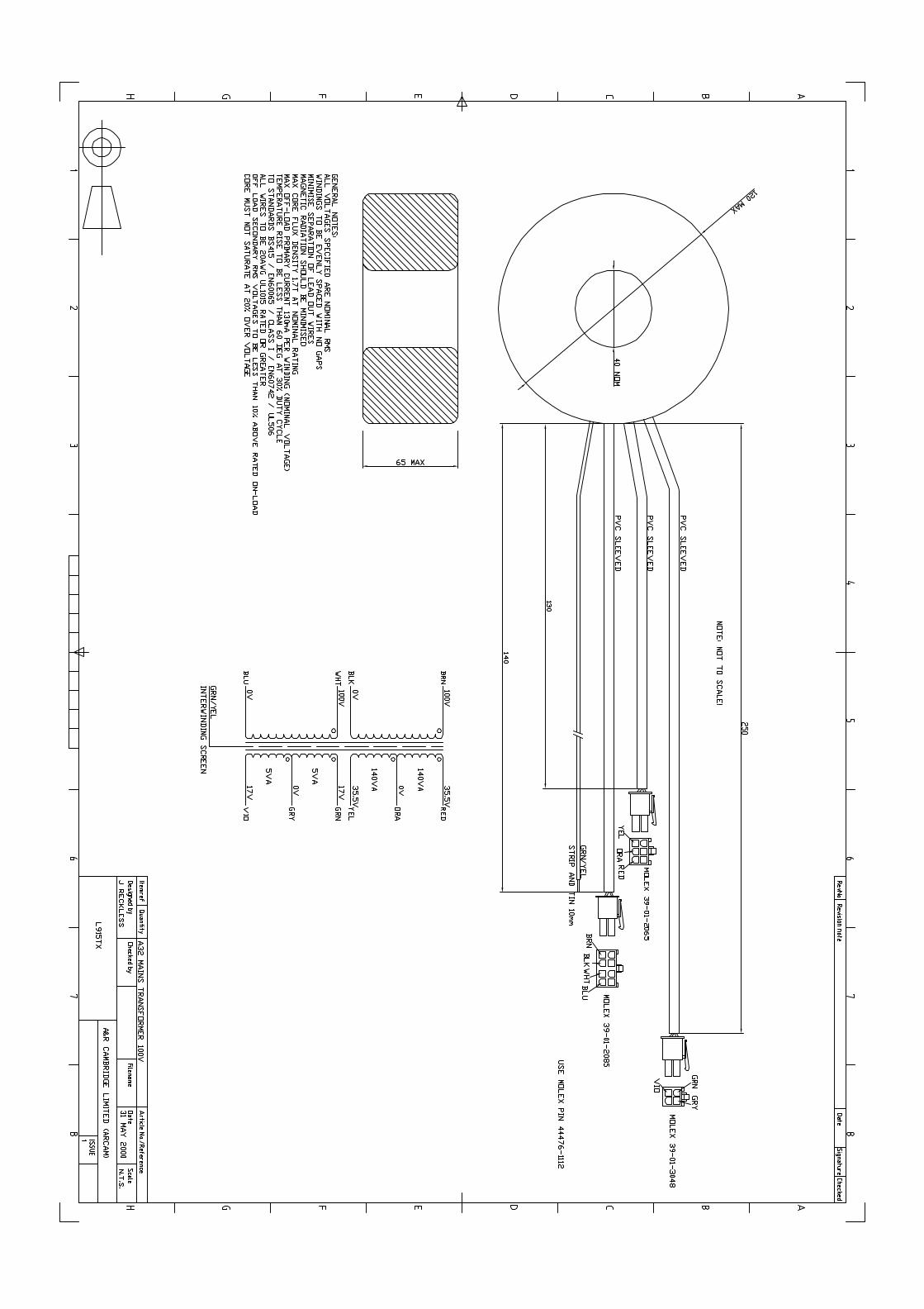
Mechanical Assembly
Contents
! General assembly parts list A32
! General assembly parts list P35
! General assembly parts list P35/3
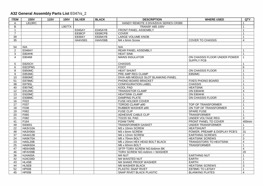
A32 General Assembly Parts List E047rs_2 ITEM 230V 115V 100V SILVER BLACK DESCRIPTION WHERE USED QTY
A L813RC HANDY REMOTE 3 DIVA/DIVA SERIES CR389 1 B L907TX TRANSF A85 100V 1 1 E045AY E045AYB FRONT PANEL ASSEMBLY 1 7 E838CP E838CPB COVER 1
39 E839AY E839AYB LARGE VOLUME KNOB 1 35 HA4V06S HA4V06B M4 x 6mm Screw COVER TO CHASSIS 4
54 N/A N/A 2 E046AY REAR PANEL ASSEMBLY 1 3 E804HK HEAT SINK 1 4 E804MI MAINS INSULATOR ON CHASSIS FLOOR UNDER POWER
SUPPLY PCB 1
5 E820CH CHASSIS 1 6 E822PM1 FOOT 6 8 E850MC HEAT SHUNT ON CHASSIS FLOOR 1 9 E853MC PRE AMP REG CLAMP E850MC 1
10 E860MC DIVA A85 MODULE SLOT BLANKING PANEL 1 51 E878MC PHONO BOARD BRACKET FIXES PHONO BOARD 1 38 E879SL CONFIGURATION LABEL CHASSIS 1 40 E907MC KOOL PAD HEATSINK 1 12 E912MC TRANSISTOR CLAMP ON E804HK 4 13 E920MC HEATSINK CLAMP ON E804HK 1 14 E938MC DAMPING PLATE ON CHASSIS FLOOR 1 16 F022 FUSE HOLDER COVER 2 17 F037 TOROID CLAMP ø90 TOP OF TRANSFORMER 1 18 F038 RUBBER WASHER ø90 ON TOP OF TRANSFORMER 1 19 F062 FUSE CLIP SPARE FUSE 1 20 F065 ADHESIVE CABLE CLIP TRANSFORMER 1 21 F082 TO220 SIL PAD UNDER VOLTAGE REG 3 41 F164 FOAM TAPE FRONT PANEL TO COVER 400mm 49 E83001 TRANSFORMER GASKET UNDER TRANSFORMER 1 22 HA3V10A M3 x 10mm SCREW HEATSHUNT 2 48 HA3V06A M3 x 6mm SCREW POWER, PREAMP & DISPLAY PCB’S 31 37 HA4A12B M4 x 12mm SCREW EARTHING SCREWS 2 24 HA5K70A M5 x 70mm BOLT HEATSINK SCREWS 3 23 HA5L20B M5 x 20mm HEX HEAD BOLT BLACK TRANSISTORS TO HEATSINK 4 25 HA6K60A M6 x 60mm BOLT TRANSFORMER 1 47 HE6V06B SFTP TORX SCREW NO.6x6mm BK 4 46 HF4V09B TORX SCREW NO.4x9mm + WASHER 20 36 HJ4A00A M4 NUT EARTHING NUT 1 42 HJ4C00D M4 WAISTED NUT EARTH 1 43 HL4SB M4 SHAKE PROOF WASHER EARTH 1 44 HL5EB M5 WASHER BLACK HEATSINK SCREWS 3 52 HP008 PLASTIC SNAP RIVET E878MC TO L870AY 1 45 HP008 SNAP RIVET BLACK PLASTIC BLANKING PLATES 4
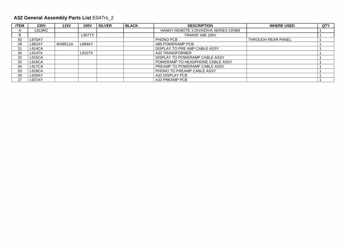
A32 General Assembly Parts List E047rs_2 ITEM 230V 115V 100V SILVER BLACK DESCRIPTION WHERE USED QTY
A L813RC HANDY REMOTE 3 DIVA/DIVA SERIES CR389 1 B L907TX TRANSF A85 100V 1 50 L870AY PHONO PCB THROUGH REAR PANEL 1 28 L882AY WA8511A L894AY A85 POWERAMP PCB 1 31 L914CA DISPLAY TO PRE AMP CABLE ASSY 1 30 L914TX L915TX A32 TRANSFORMER 1 32 L915CA DISPLAY TO POWERAMP CABLE ASSY 1 33 L916CA POWERAMP TO HEADPHONE CABLE ASSY 1 34 L917CA PREAMP TO POWERAMP CABLE ASSY 1 53 L918CA PHONO TO PREAMP CABLE ASSY 1 29 L928AY A32 DISPLAY PCB 1 27 L937AY A32 PREAMP PCB 1
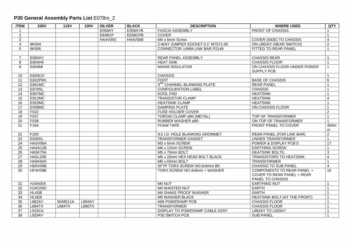
P35 General Assembly Parts List E078rs_2 ITEM 230V 115V 100V SILVER BLACK DESCRIPTION WHERE USED QTY
1 E058AY E058AYB FASCIA ASSEMBLY FRONT OF CHASSIS 1 2 E838CP E838CPB COVER 1 3 HA4V06S HA4V06B M4 x 6mm Screw COVER (SIDE) TO CHASSIS 4 4 8K004 2-WAY JUMPER SOCKET 0.1” M7571-05 ON L882AY (NEAR SWITCH) 2 5 8K006 CONNECTOR 14MM LINK BAR P2148 FITTED TO REAR PANEL 1
7 E060AY REAR PANEL ASSEMBLY CHASSIS REAR 1 8 E804HK HEAT SINK CHASSIS FLOOR 1 9 E804MI MAINS INSULATOR ON CHASSIS FLOOR UNDER POWER
SUPPLY PCB 1
10 E820CH CHASSIS 1 11 E822PM1 FOOT BASE OF CHASSIS 6 12 E861MC 3RD CHANNEL BLANKING PLATE REAR PANEL 1 13 E879SL CONFIGURATION LABEL CHASSIS 1 14 E907MC KOOL PAD HEATSINK 1 15 E912MC TRANSISTOR CLAMP HEATSINK 4 16 E920MC HEATSINK CLAMP HEATSINK 1 17 E938MC DAMPING PLATE ON CHASSIS FLOOR 1 18 F022 FUSE HOLDER COVER 2 19 F037 TOROID CLAMP ø90 (METAL) TOP OF TRANSFORMER 1 20 F038 RUBBER WASHER ø90 ON TOP OF TRANSFORMER 1 21 F164 FOAM TAPE FRONT PANEL TO COVER 400m
m 22 F200 9,5 I.D. HOLE BLANKING GROMMET REAR PANEL (FOR LINK BAR) 2 23 E83001 TRANSFORMER GASKET UNDER TRANSFORMER 1 24 HA3V06A M3 x 6mm SCREW POWER & DISPLAY PCB’S 17 25 HA4A12B M4 x 12mm SCREW EARTHING SCREW 1 26 HA5K70A M5 x 70mm BOLT HEATSINK BOLTS 3 27 HA5L20B M5 x 20mm HEX HEAD BOLT BLACK TRANSISTORS TO HEATSINK 4 28 HA6K60A M6 x 60mm BOLT TRANSFORMER 1 29 HE6V06B SFTP TORX SCREW NO.6x6mm BK CHASSIS TO SUB PANEL 4 30 HF4V09B TORX SCREW NO.4x9mm + WASHER COMPONENTS TO REAR PANEL +
COVER TO REAR PANEL + REAR PANEL TO CHASSIS
16
31 HJ4A00A M4 NUT EARTHING NUT 1 32 HJ4C00D M4 WAISTED NUT EARTH 1 33 HL4SB M4 SHAKE PROOF WASHER EARTH 1 34 HL5EB M5 WASHER BLACK HEATSINK BOLT (AT THE FRONT) 1 35 L882AY WA8511A L894AY A85 POWERAMP PCB CHASSIS FLOOR 1 36 L884TX L884TX L880TX TRANSFORMER CHASSIS FLOOR 1 37 L915CA DISPLAY TO POWERAMP CABLE ASSY L882AY TO L929AY 1 38 L929AY P35 SWITCH PCB SUB PANEL 1
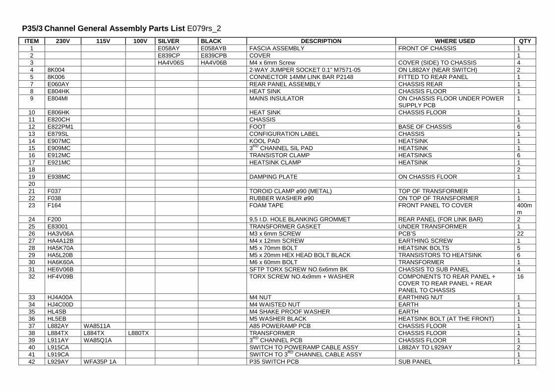
P35/3 Channel General Assembly Parts List E079rs_2 ITEM 230V 115V 100V SILVER BLACK DESCRIPTION WHERE USED QTY
1 E058AY E058AYB FASCIA ASSEMBLY FRONT OF CHASSIS 1 2 E839CP E839CPB COVER 1 3 HA4V06S HA4V06B M4 x 6mm Screw COVER (SIDE) TO CHASSIS 4 4 8K004 2-WAY JUMPER SOCKET 0.1” M7571-05 ON L882AY (NEAR SWITCH) 2 5 8K006 CONNECTOR 14MM LINK BAR P2148 FITTED TO REAR PANEL 1 7 E060AY REAR PANEL ASSEMBLY CHASSIS REAR 1 8 E804HK HEAT SINK CHASSIS FLOOR 1 9 E804MI MAINS INSULATOR ON CHASSIS FLOOR UNDER POWER
SUPPLY PCB 1
10 E806HK HEAT SINK CHASSIS FLOOR 1 11 E820CH CHASSIS 1 12 E822PM1 FOOT BASE OF CHASSIS 6 13 E879SL CONFIGURATION LABEL CHASSIS 1 14 E907MC KOOL PAD HEATSINK 1 15 E909MC 3RD CHANNEL SIL PAD HEATSINK 1 16 E912MC TRANSISTOR CLAMP HEATSINKS 6 17 E921MC HEATSINK CLAMP HEATSINK 1 18 2 19 E938MC DAMPING PLATE ON CHASSIS FLOOR 1 20 21 F037 TOROID CLAMP ø90 (METAL) TOP OF TRANSFORMER 1 22 F038 RUBBER WASHER ø90 ON TOP OF TRANSFORMER 1 23 F164 FOAM TAPE FRONT PANEL TO COVER 400m
m 24 F200 9,5 I.D. HOLE BLANKING GROMMET REAR PANEL (FOR LINK BAR) 2 25 E83001 TRANSFORMER GASKET UNDER TRANSFORMER 1 26 HA3V06A M3 x 6mm SCREW PCB’S 22 27 HA4A12B M4 x 12mm SCREW EARTHING SCREW 1 28 HA5K70A M5 x 70mm BOLT HEATSINK BOLTS 5 29 HA5L20B M5 x 20mm HEX HEAD BOLT BLACK TRANSISTORS TO HEATSINK 6 30 HA6K60A M6 x 60mm BOLT TRANSFORMER 1 31 HE6V06B SFTP TORX SCREW NO.6x6mm BK CHASSIS TO SUB PANEL 4 32 HF4V09B TORX SCREW NO.4x9mm + WASHER COMPONENTS TO REAR PANEL +
COVER TO REAR PANEL + REAR PANEL TO CHASSIS
16
33 HJ4A00A M4 NUT EARTHING NUT 1 34 HJ4C00D M4 WAISTED NUT EARTH 1 35 HL4SB M4 SHAKE PROOF WASHER EARTH 1 36 HL5EB M5 WASHER BLACK HEATSINK BOLT (AT THE FRONT) 1 37 L882AY WA8511A A85 POWERAMP PCB CHASSIS FLOOR 1 38 L884TX L884TX L880TX TRANSFORMER CHASSIS FLOOR 1 39 L911AY WA85Q1A 3RD CHANNEL PCB CHASSIS FLOOR 1 40 L915CA SWITCH TO POWERAMP CABLE ASSY L882AY TO L929AY 2 41 L919CA SWITCH TO 3RD CHANNEL CABLE ASSY 1 42 L929AY WFA35P 1A P35 SWITCH PCB SUB PANEL 1

ARCAM
All parts can be ordered via [email protected]
Pembroke Ave, Waterbeach, Cambridge, CB5 9PB, ENGLAND TEL: +44(0) 1223 203 203 FAX: +44(0) 1223 863 384