Embed Size (px)
Citation preview
Fujitsu Microelectronics Europe Application Note
MCU-AN-300205-E-V16
F²MC-16FX FAMILY 16-BIT MICROCONTROLLER
ALL SERIES
USART
APPLICATION NOTE
USART Revision History
MCU-AN-300205-E-V16 - 2 - © Fujitsu Microelectronics Europe GmbH
Revision History
Date Issue 2006-04-28 First Version; MWi 2006-12-07 V1.1, Reviewed the document and updated with review findings, MPi 2007-02-21 V1.2, Updated with re-review findings, MPi
Added clock modulator related information, MPi 2007-08-29 V1.3, Added schematic, error conditions and updated register related
information, MPi 2007-10-10 V1.4, Timing diagrams updated, MWi 2008-07-07 V1.5, Add information on PIER; PHu 2010-02-19 V1.6, DMA transmission sub chapter and example code added; MWi
This document contains 32 pages.
USART Warranty and Disclaimer
© Fujitsu Microelectronics Europe GmbH - 3 - MCU-AN-300205-E-V16
Warranty and Disclaimer To the maximum extent permitted by applicable law, Fujitsu Microelectronics Europe GmbH restricts its warranties and its liability for all products delivered free of charge (e.g. software include or header files, application examples, target boards, evaluation boards, engineering samples of IC’s etc.), its performance and any consequential damages, on the use of the Product in accordance with (i) the terms of the License Agreement and the Sale and Purchase Agreement under which agreements the Product has been delivered, (ii) the technical descriptions and (iii) all accompanying written materials. In addition, to the maximum extent permitted by applicable law, Fujitsu Microelectronics Europe GmbH disclaims all warranties and liabilities for the performance of the Product and any consequential damages in cases of unauthorised decompiling and/or reverse engineering and/or disassembling. Note, all these products are intended and must only be used in an evaluation laboratory environment.
1. Fujitsu Microelectronics Europe GmbH warrants that the Product will perform substantially in accordance with the accompanying written materials for a period of 90 days form the date of receipt by the customer. Concerning the hardware components of the Product, Fujitsu Microelectronics Europe GmbH warrants that the Product will be free from defects in material and workmanship under use and service as specified in the accompanying written materials for a duration of 1 year from the date of receipt by the customer.
2. Should a Product turn out to be defect, Fujitsu Microelectronics Europe GmbH´s entire liability and the customer’s exclusive remedy shall be, at Fujitsu Microelectronics Europe GmbH´s sole discretion, either return of the purchase price and the license fee, or replacement of the Product or parts thereof, if the Product is returned to Fujitsu Microelectronics Europe GmbH in original packing and without further defects resulting from the customer’s use or the transport. However, this warranty is excluded if the defect has resulted from an accident not attributable to Fujitsu Microelectronics Europe GmbH, or abuse or misapplication attributable to the customer or any other third party not relating to Fujitsu Microelectronics Europe GmbH.
3. To the maximum extent permitted by applicable law Fujitsu Microelectronics Europe GmbH disclaims all other warranties, whether expressed or implied, in particular, but not limited to, warranties of merchantability and fitness for a particular purpose for which the Product is not designated.
4. To the maximum extent permitted by applicable law, Fujitsu Microelectronics Europe GmbH´s and its suppliers´ liability is restricted to intention and gross negligence.
NO LIABILITY FOR CONSEQUENTIAL DAMAGES
To the maximum extent permitted by applicable law, in no event shall Fujitsu Microelectronics Europe GmbH and its suppliers be liable for any damages whatsoever (including but without limitation, consequential and/or indirect damages for personal injury, assets of substantial value, loss of profits, interruption of business operation, loss of information, or any other monetary or pecuniary loss) arising from the use of the Product.
Should one of the above stipulations be or become invalid and/or unenforceable, the remaining stipulations shall stay in full effect
USART Contents
MCU-AN-300205-E-V16 - 4 - © Fujitsu Microelectronics Europe GmbH
Contents
REVISION HISTORY.............................................................................................................. 2
WARRANTY AND DISCLAIMER........................................................................................... 3
CONTENTS ............................................................................................................................ 4
1 INTRODUCTION................................................................................................................ 6 1.1 Key Features............................................................................................................. 6
2 THE USART WITH LIN FUNCTIONALITY........................................................................ 7 2.1 Block Diagram........................................................................................................... 7 2.2 Basic Functionality .................................................................................................... 8 2.3 Registers................................................................................................................... 8
2.3.1 Serial Control Register (SCR) ...................................................................... 8 2.3.2 Serial Mode Register (SMR)......................................................................... 9 2.3.3 Serial Status register (SSR) ....................................................................... 10 2.3.4 Reception Data Register (RDR) ................................................................. 10 2.3.5 Transmission Data Register (TDR) ............................................................ 10 2.3.6 Extended Status/Control Register (ESCR) ............................................... 11
2.3.6.1 LIN Break Detection Consideration........................................... 11 2.3.7 Extended Communication Control register (ECCR) ................................... 12 2.3.8 Baud Rate Generator Register (BGR)........................................................ 13
2.3.8.1 Minimum and Maximum Ratings............................................... 13 2.4 Error Conditions ...................................................................................................... 13
2.4.1 Clearing Reception Errors and De-synchronization .................................. 13 2.4.2 USART Dominant Bus Behavior ............................................................... 15
2.5 Interface to the BUS................................................................................................ 17 2.5.1 RS232 ....................................................................................................... 17 2.5.2 LIN............................................................................................................. 18
2.6 DMA Transmission with USART ............................................................................. 19
3 USART EXAMPLES ........................................................................................................ 21 3.1 Asynchronous Mode (0) without Interrupts ............................................................. 21 3.2 Asynchronous Mode (0) with Interrupts .................................................................. 22 3.3 Synchronous Mode (SPI) Master without Interrupts ............................................... 24 3.4 DMA block transmission.......................................................................................... 27
4 APPENDIX A ................................................................................................................... 29 4.1 Related Documents................................................................................................. 29
USART Contents
© Fujitsu Microelectronics Europe GmbH - 5 - MCU-AN-300205-E-V16
5 ADDITIONAL INFORMATION......................................................................................... 30
LIST OF FIGURES ............................................................................................................... 31
LIST OF TABLES................................................................................................................. 32
USART Chapter 1 Introduction
MCU-AN-300205-E-V16 - 6 - © Fujitsu Microelectronics Europe GmbH
1 Introduction This application note describes the functionality of the USART and their operation modes and gives some examples.
1.1 Key Features • Full Duplex
• NRZ/RZ for serial Data In- and Output
• NRZ/RZ for serial Clock In- and Output
• Asynchronous and synchronous Mode
• 7-8 Data Bits and 1-2 Stop Bits for asynchronous mode, even or odd Parity selectable
• Dedicated Reload Counter as Clock Divider for Baud Rate (610 Bits/s up to 4 MBits/s synchronous at 20 MHz Peripheral Clock)
• Reload Counter can be fed with external clock
• Synchronous master or slave capable
• 4 SPI Clock Modes
• Framing, Overrun, and Parity Error detectable
• LIN Synch Break Detection and Generation (13, 14, 15, 16 Bit Times selectable)
• LIN Synch Field Signal can be fed to Input Capture Unit for Time Measurement
• Start and Stop Bits selectable in synchronous Mode
• Continuous Serial Clock Output selectable in synchronous Mode
• Asynchronous Master-Slave Communication (Address and Data Bit selectable)
USART Chapter 2 The USART with LIN functionality
© Fujitsu Microelectronics Europe GmbH - 7 - MCU-AN-300205-E-V16
2 The USART with LIN functionality
THE BASIC FUNCTIONALITY OF THE USART WITH LIN FUNCTIONALITY
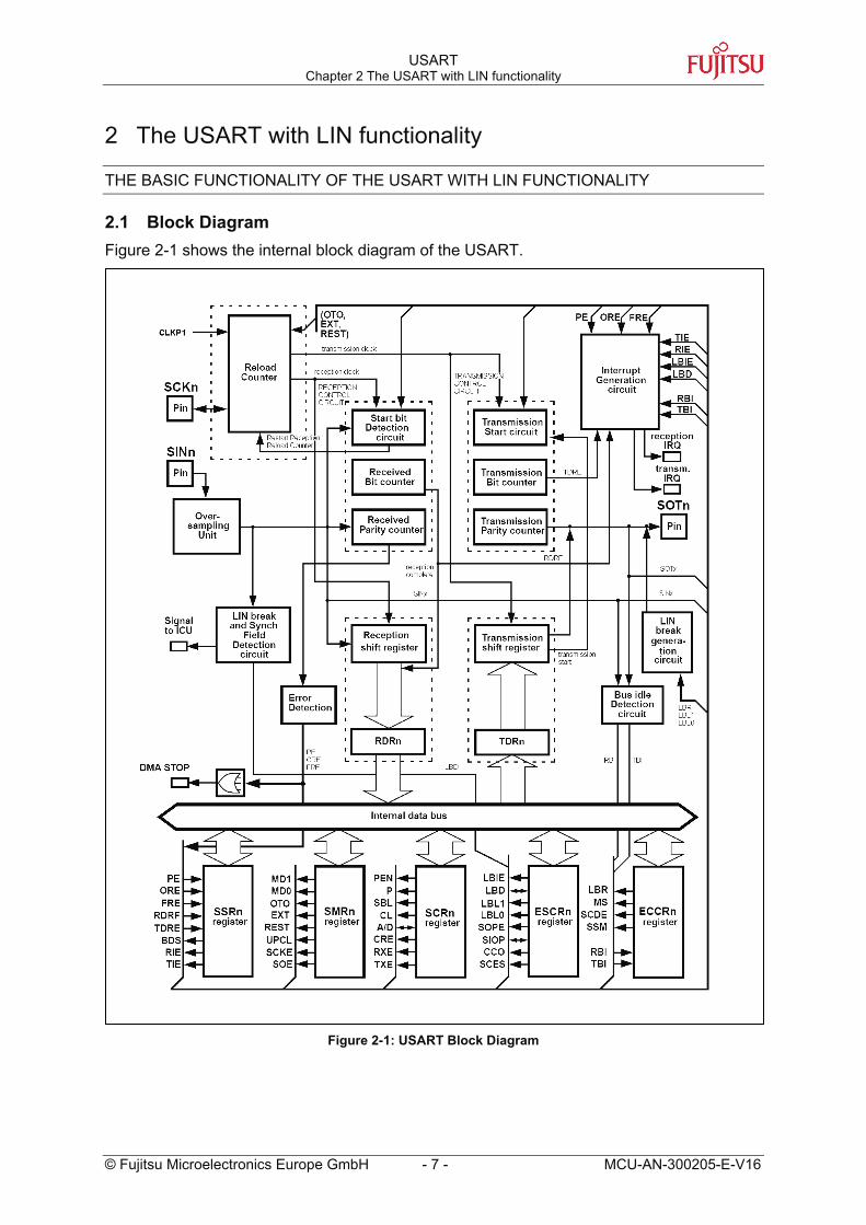
2.1 Block Diagram Figure 2-1 shows the internal block diagram of the USART.
Figure 2-1: USART Block Diagram
USART Chapter 2 The USART with LIN functionality
MCU-AN-300205-E-V16 - 8 - © Fujitsu Microelectronics Europe GmbH
2.2 Basic Functionality The USART has four different operation modes, which are selectable via the MD[1:0] bits in the Serial Mode Register (SMR) 2.3.2.
MD1 MD0 Mode Description 0 0 0 Asynchronous (normal mode) 0 1 1 Asynchronous (Master/Slave Mode) 1 0 2 Synchronous Mode 1 1 3 Asynchronous (LIN Mode)
Table 2-1: USART Operation Modes
Please change the mode only when USART reception and transmission is off (SCR:RXE = 0, SCR:TXE = 0). Furthermore it is recommended to reset the USART with the SMR:UPCL bit, after operation mode has changed.
Example:
2.3 Registers Please note that any changes in the settings of the USART should be done while reception as well as transmission is disabled (RXE = 0, TXE = 0). Otherwise the result of ongoing reception / transmission might be incorrect and the USART might not be initialized correctly.
2.3.1 Serial Control Register (SCR)Bit No. Name Explanation Value Operation
0 Parity disabled 7 PEN Parity Enable*1
1 Parity enabled 0 Even Parity enabled 6 P Parity Even/Odd Selection*1
1 Odd Parity enabled 0 1 Stop bit selected 5 SBL Stop Bit Length*2
1 2 Stop bits selected 0 7 Bits 4 CL Character Length*3
1 8 Bits 0 Data Bit 3 AD Address/Data Bit*4
1 Address Bit 0 Write: No effect
2 CRE Clear Reception Errors 1 Write: Errors cleared, Reception is reset
0 Reception disabled 1 RXE Reception Enable 1 Reception enabled 0 Transmission disabled 0 TXE Transmission Enable 1 Transmission enabled
Table 2-2: SCR
Note: When enabling reception, please also enable the corresponding input pin with its Port Input Enable Register (PIER) bit. *1 This function is only available in Mode 0 and 2 if SSM = 1.*2 This function is only available in Mode 0, 1 and 2 if SSM = 1.*3 This function is only available in Mode 0 and 1. *4 This function is only available in Mode 1.
. . .SMR0 = 0x83; // Set USART to Mode 2 (synchronous operation), serial output &
// serial clock output enabled SMR0 = 0x87; // Reset USART (UPCL bit#2 is auto-cleared)
. . .
USART Chapter 2 The USART with LIN functionality
© Fujitsu Microelectronics Europe GmbH - 9 - MCU-AN-300205-E-V16
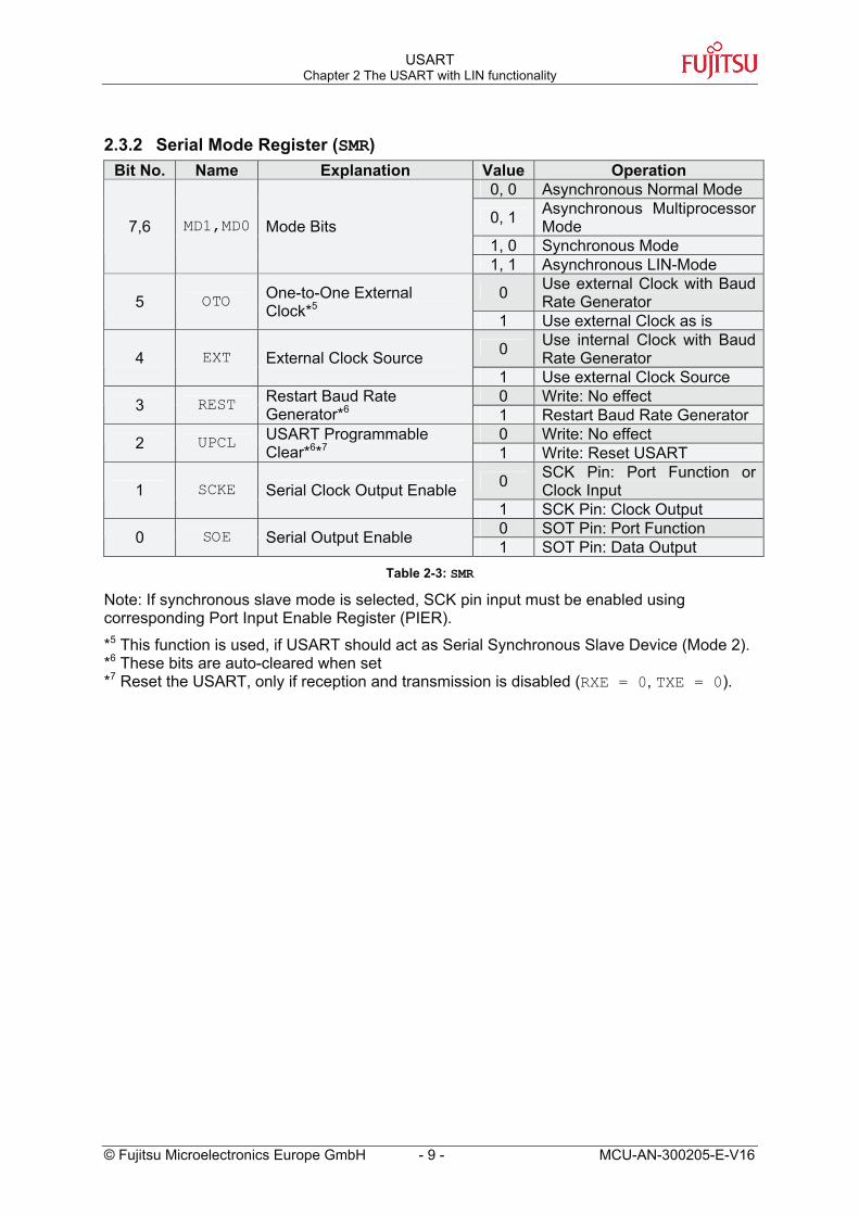
2.3.2 Serial Mode Register (SMR)Bit No. Name Explanation Value Operation
0, 0 Asynchronous Normal Mode
0, 1 Asynchronous Multiprocessor Mode
1, 0 Synchronous Mode 7,6 MD1,MD0 Mode Bits
1, 1 Asynchronous LIN-Mode
0 Use external Clock with Baud Rate Generator 5 OTO One-to-One External
Clock*5
1 Use external Clock as is
0 Use internal Clock with Baud Rate Generator 4 EXT External Clock Source
1 Use external Clock Source 0 Write: No effect 3 REST Restart Baud Rate
Generator*6 1 Restart Baud Rate Generator 0 Write: No effect 2 UPCL USART Programmable
Clear*6*7 1 Write: Reset USART
0 SCK Pin: Port Function or Clock Input 1 SCKE Serial Clock Output Enable
1 SCK Pin: Clock Output 0 SOT Pin: Port Function 0 SOE Serial Output Enable 1 SOT Pin: Data Output
Table 2-3: SMR
Note: If synchronous slave mode is selected, SCK pin input must be enabled using corresponding Port Input Enable Register (PIER).
*5 This function is used, if USART should act as Serial Synchronous Slave Device (Mode 2). *6 These bits are auto-cleared when set *7 Reset the USART, only if reception and transmission is disabled (RXE = 0, TXE = 0).
USART Chapter 2 The USART with LIN functionality
MCU-AN-300205-E-V16 - 10 - © Fujitsu Microelectronics Europe GmbH
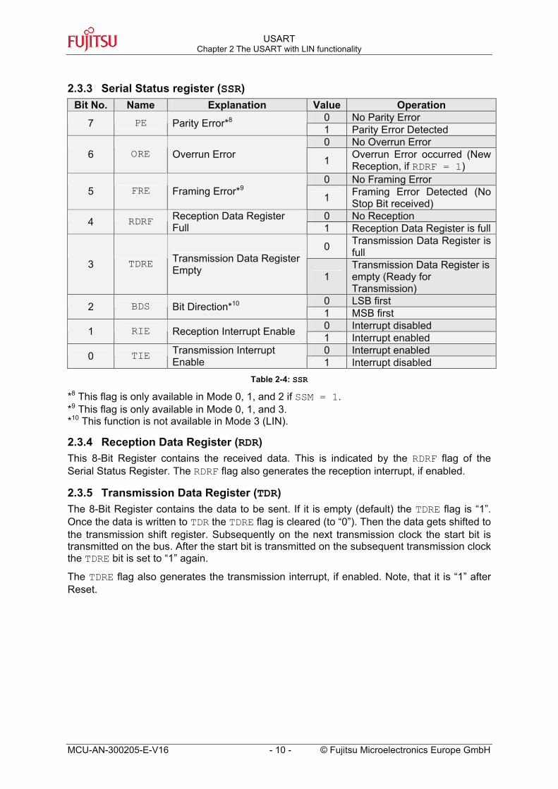
2.3.3 Serial Status register (SSR)Bit No. Name Explanation Value Operation
0 No Parity Error 7 PE Parity Error*8
1 Parity Error Detected 0 No Overrun Error
6 ORE Overrun Error 1 Overrun Error occurred (New Reception, if RDRF = 1)
0 No Framing Error 5 FRE Framing Error*9
1 Framing Error Detected (No Stop Bit received)
0 No Reception 4 RDRF Reception Data Register Full 1 Reception Data Register is full
0 Transmission Data Register is full
3 TDRE Transmission Data Register Empty 1
Transmission Data Register is empty (Ready for Transmission)
0 LSB first 2 BDS Bit Direction*10 1 MSB first 0 Interrupt disabled 1 RIE Reception Interrupt Enable 1 Interrupt enabled 0 Interrupt enabled 0 TIE Transmission Interrupt
Enable 1 Interrupt disabled Table 2-4: SSR
*8 This flag is only available in Mode 0, 1, and 2 if SSM = 1.*9 This flag is only available in Mode 0, 1, and 3. *10 This function is not available in Mode 3 (LIN).
2.3.4 Reception Data Register (RDR)This 8-Bit Register contains the received data. This is indicated by the RDRF flag of the Serial Status Register. The RDRF flag also generates the reception interrupt, if enabled.
2.3.5 Transmission Data Register (TDR)The 8-Bit Register contains the data to be sent. If it is empty (default) the TDRE flag is “1”. Once the data is written to TDR the TDRE flag is cleared (to “0”). Then the data gets shifted to the transmission shift register. Subsequently on the next transmission clock the start bit is transmitted on the bus. After the start bit is transmitted on the subsequent transmission clock the TDRE bit is set to “1” again.
The TDRE flag also generates the transmission interrupt, if enabled. Note, that it is “1” after Reset.
USART Chapter 2 The USART with LIN functionality
© Fujitsu Microelectronics Europe GmbH - 11 - MCU-AN-300205-E-V16
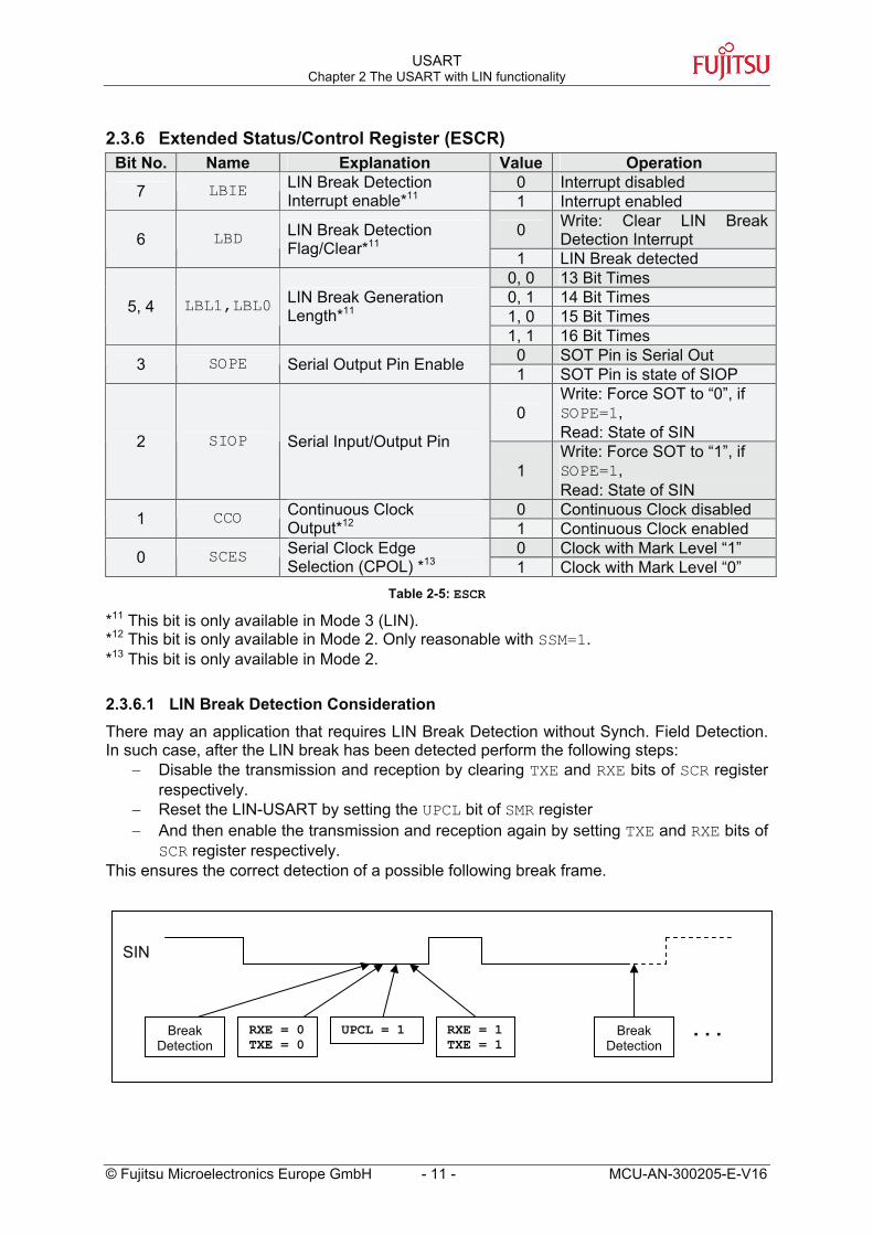
2.3.6 Extended Status/Control Register (ESCR) Bit No. Name Explanation Value Operation
0 Interrupt disabled 7 LBIE LIN Break Detection Interrupt enable*11 1 Interrupt enabled
0 Write: Clear LIN Break Detection Interrupt 6 LBD LIN Break Detection
Flag/Clear*11
1 LIN Break detected 0, 0 13 Bit Times 0, 1 14 Bit Times 1, 0 15 Bit Times 5, 4 LBL1,LBL0 LIN Break Generation
Length*11 1, 1 16 Bit Times 0 SOT Pin is Serial Out 3 SOPE Serial Output Pin Enable 1 SOT Pin is state of SIOP
0Write: Force SOT to “0”, if SOPE=1,Read: State of SIN 2 SIOP Serial Input/Output Pin
1Write: Force SOT to “1”, if SOPE=1,Read: State of SIN
0 Continuous Clock disabled 1 CCO Continuous Clock Output*12 1 Continuous Clock enabled
0 Clock with Mark Level “1” 0 SCES Serial Clock Edge Selection (CPOL) *13 1 Clock with Mark Level “0”
Table 2-5: ESCR
*11 This bit is only available in Mode 3 (LIN). *12 This bit is only available in Mode 2. Only reasonable with SSM=1.*13 This bit is only available in Mode 2.
2.3.6.1 LIN Break Detection Consideration There may an application that requires LIN Break Detection without Synch. Field Detection. In such case, after the LIN break has been detected perform the following steps:
− Disable the transmission and reception by clearing TXE and RXE bits of SCR register respectively.
− Reset the LIN-USART by setting the UPCL bit of SMR register − And then enable the transmission and reception again by setting TXE and RXE bits of
SCR register respectively. This ensures the correct detection of a possible following break frame.
Break Detection
RXE = 0TXE = 0
UPCL = 1 RXE = 1TXE = 1
Break Detection
. . .
SIN
USART Chapter 2 The USART with LIN functionality
MCU-AN-300205-E-V16 - 12 - © Fujitsu Microelectronics Europe GmbH
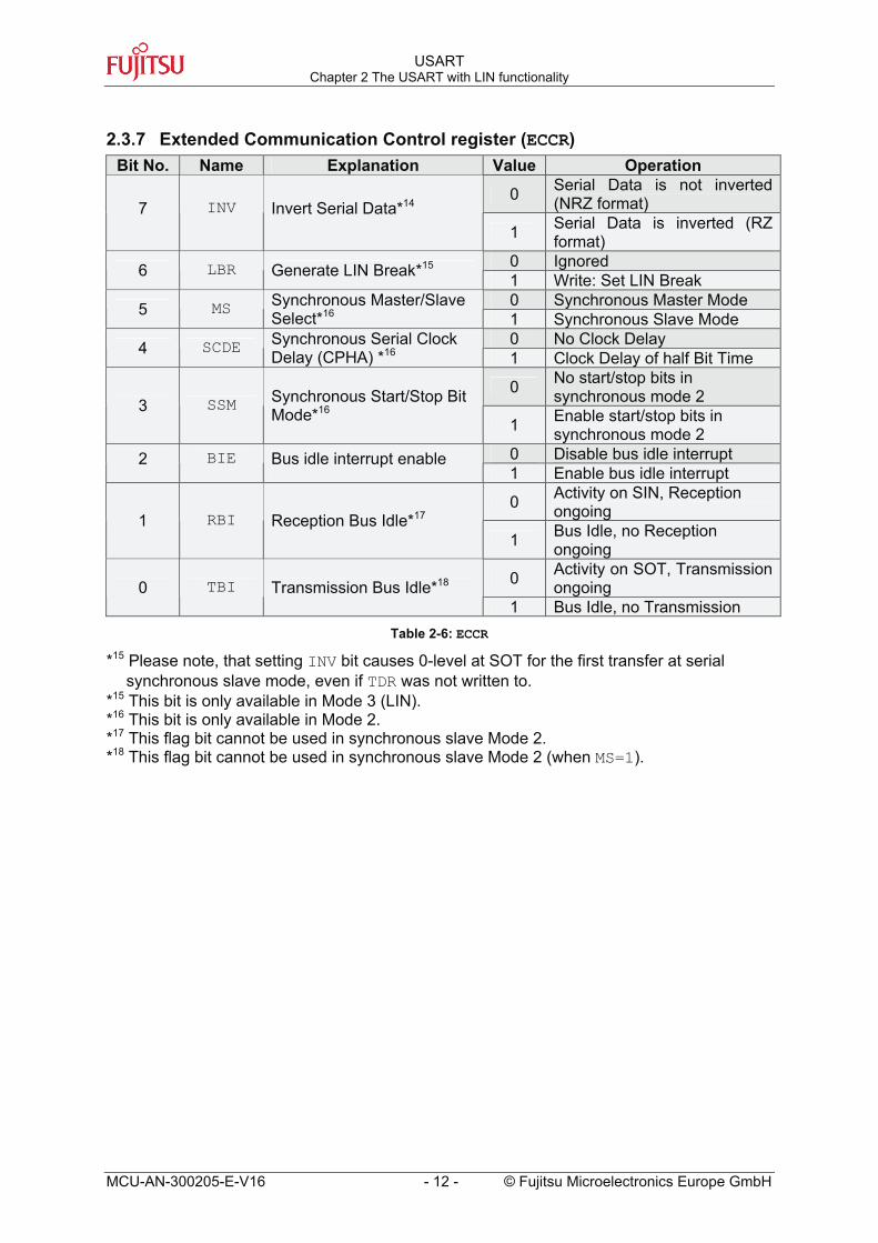
2.3.7 Extended Communication Control register (ECCR)Bit No. Name Explanation Value Operation
0 Serial Data is not inverted (NRZ format) 7 INV Invert Serial Data*14
1 Serial Data is inverted (RZ format)
0 Ignored 6 LBR Generate LIN Break*15 1 Write: Set LIN Break 0 Synchronous Master Mode 5 MS Synchronous Master/Slave
Select*16 1 Synchronous Slave Mode 0 No Clock Delay 4 SCDE Synchronous Serial Clock
Delay (CPHA) *16 1 Clock Delay of half Bit Time
0 No start/stop bits in synchronous mode 2 3 SSM Synchronous Start/Stop Bit
Mode*16 1 Enable start/stop bits in synchronous mode 2
0 Disable bus idle interrupt 2 BIE Bus idle interrupt enable 1 Enable bus idle interrupt
0 Activity on SIN, Reception ongoing 1 RBI Reception Bus Idle*17
1 Bus Idle, no Reception ongoing
0 Activity on SOT, Transmission ongoing 0 TBI Transmission Bus Idle*18
1 Bus Idle, no Transmission Table 2-6: ECCR
*15 Please note, that setting INV bit causes 0-level at SOT for the first transfer at serial synchronous slave mode, even if TDR was not written to.
*15 This bit is only available in Mode 3 (LIN). *16 This bit is only available in Mode 2. *17 This flag bit cannot be used in synchronous slave Mode 2. *18 This flag bit cannot be used in synchronous slave Mode 2 (when MS=1).
USART Chapter 2 The USART with LIN functionality
© Fujitsu Microelectronics Europe GmbH - 13 - MCU-AN-300205-E-V16
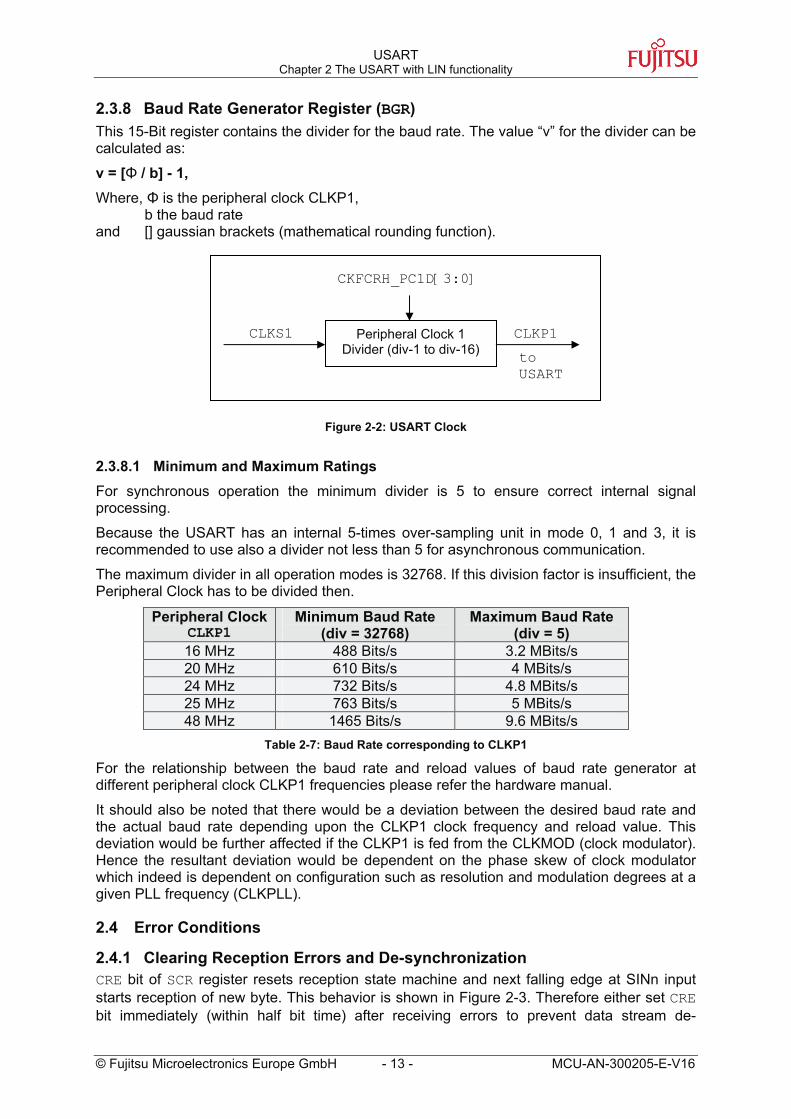
2.3.8 Baud Rate Generator Register (BGR)This 15-Bit register contains the divider for the baud rate. The value “v” for the divider can be calculated as:
v = [Φ / b] - 1, Where, Φ is the peripheral clock CLKP1, b the baud rate and [] gaussian brackets (mathematical rounding function).
Figure 2-2: USART Clock
2.3.8.1 Minimum and Maximum Ratings For synchronous operation the minimum divider is 5 to ensure correct internal signal processing.
Because the USART has an internal 5-times over-sampling unit in mode 0, 1 and 3, it is recommended to use also a divider not less than 5 for asynchronous communication.
The maximum divider in all operation modes is 32768. If this division factor is insufficient, the Peripheral Clock has to be divided then.
Peripheral ClockCLKP1
Minimum Baud Rate (div = 32768)
Maximum Baud Rate (div = 5)
16 MHz 488 Bits/s 3.2 MBits/s 20 MHz 610 Bits/s 4 MBits/s 24 MHz 732 Bits/s 4.8 MBits/s 25 MHz 763 Bits/s 5 MBits/s 48 MHz 1465 Bits/s 9.6 MBits/s
Table 2-7: Baud Rate corresponding to CLKP1
For the relationship between the baud rate and reload values of baud rate generator at different peripheral clock CLKP1 frequencies please refer the hardware manual.
It should also be noted that there would be a deviation between the desired baud rate and the actual baud rate depending upon the CLKP1 clock frequency and reload value. This deviation would be further affected if the CLKP1 is fed from the CLKMOD (clock modulator). Hence the resultant deviation would be dependent on the phase skew of clock modulator which indeed is dependent on configuration such as resolution and modulation degrees at a given PLL frequency (CLKPLL).
2.4 Error Conditions
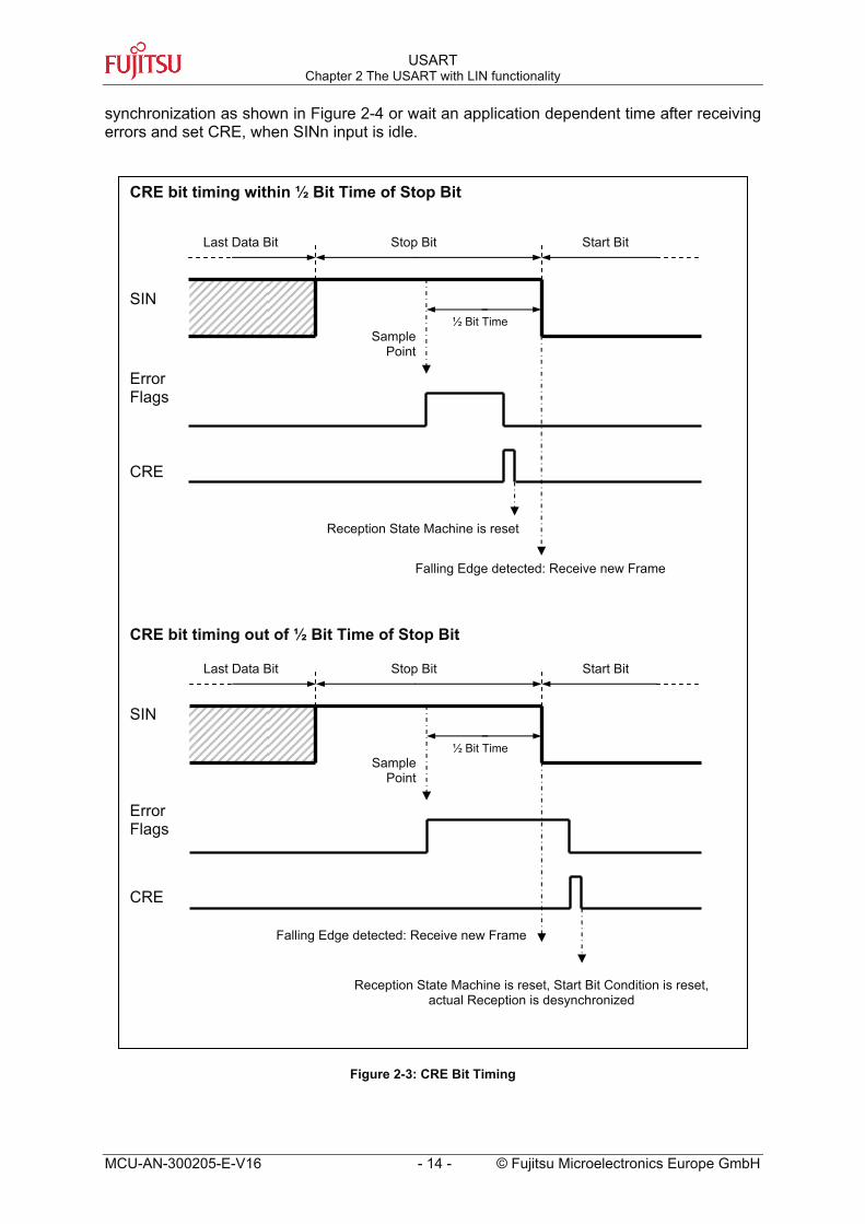
2.4.1 Clearing Reception Errors and De-synchronization CRE bit of SCR register resets reception state machine and next falling edge at SINn input starts reception of new byte. This behavior is shown in Figure 2-3. Therefore either set CRE bit immediately (within half bit time) after receiving errors to prevent data stream de-
Peripheral Clock 1 Divider (div-1 to div-16)
CKFCRH_PC1D[3:0]
CLKS1 CLKP1to USART
USART Chapter 2 The USART with LIN functionality
MCU-AN-300205-E-V16 - 14 - © Fujitsu Microelectronics Europe GmbH
synchronization as shown in Figure 2-4 or wait an application dependent time after receiving errors and set CRE, when SINn input is idle.
Figure 2-3: CRE Bit Timing
CRE bit timing within ½ Bit Time of Stop Bit
SIN
Error Flags
CRE
CRE bit timing out of ½ Bit Time of Stop Bit
SIN
Error Flags
CRE
Last Data Bit Stop Bit Start Bit
Sample Point
½ Bit Time
Falling Edge detected: Receive new Frame
Reception State Machine is reset
Last Data Bit Stop Bit Start Bit
Sample Point
½ Bit Time
Falling Edge detected: Receive new Frame
Reception State Machine is reset, Start Bit Condition is reset, actual Reception is desynchronized
USART Chapter 2 The USART with LIN functionality
© Fujitsu Microelectronics Europe GmbH - 15 - MCU-AN-300205-E-V16
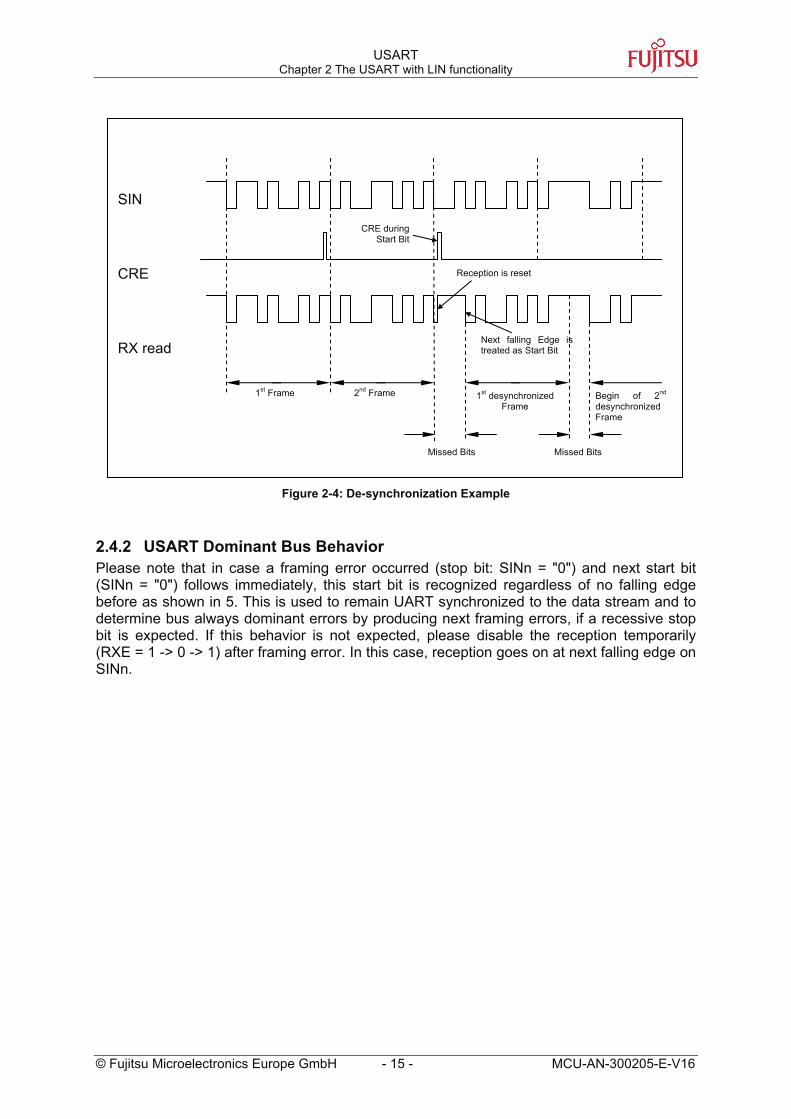
Figure 2-4: De-synchronization Example
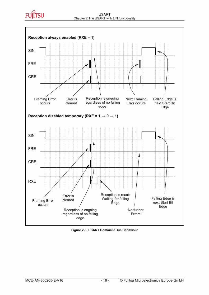
2.4.2 USART Dominant Bus Behavior Please note that in case a framing error occurred (stop bit: SINn = "0") and next start bit (SINn = "0") follows immediately, this start bit is recognized regardless of no falling edge before as shown in 5. This is used to remain UART synchronized to the data stream and to determine bus always dominant errors by producing next framing errors, if a recessive stop bit is expected. If this behavior is not expected, please disable the reception temporarily (RXE = 1 -> 0 -> 1) after framing error. In this case, reception goes on at next falling edge on SINn.
SIN
CRE
RX read
CRE during Start Bit
Reception is reset
Next falling Edge istreated as Start Bit
1st Frame 2nd Frame 1st desynchronized Frame
Begin of 2nd
desynchronized Frame
Missed Bits Missed Bits
USART Chapter 2 The USART with LIN functionality
MCU-AN-300205-E-V16 - 16 - © Fujitsu Microelectronics Europe GmbH
Figure 2-5: USART Dominant Bus Behaviour
Reception always enabled (RXE = 1)
SIN
FRE
CRE
Reception disabled temporary (RXE = 1 → 0 → 1)
SIN
FRE
CRE
RXE
Framing Error occurs
Error is cleared
Reception is ongoing regardless of no falling
edge
Next Framing Error occurs
Falling Edge is next Start Bit
Edge
Framing Error occurs
Error is cleared
Reception is ongoing regardless of no falling
edge
Reception is reset: Waiting for falling
Edge
No further Errors
Falling Edge is next Start Bit
Edge
USART Chapter 2 The USART with LIN functionality
© Fujitsu Microelectronics Europe GmbH - 17 - MCU-AN-300205-E-V16
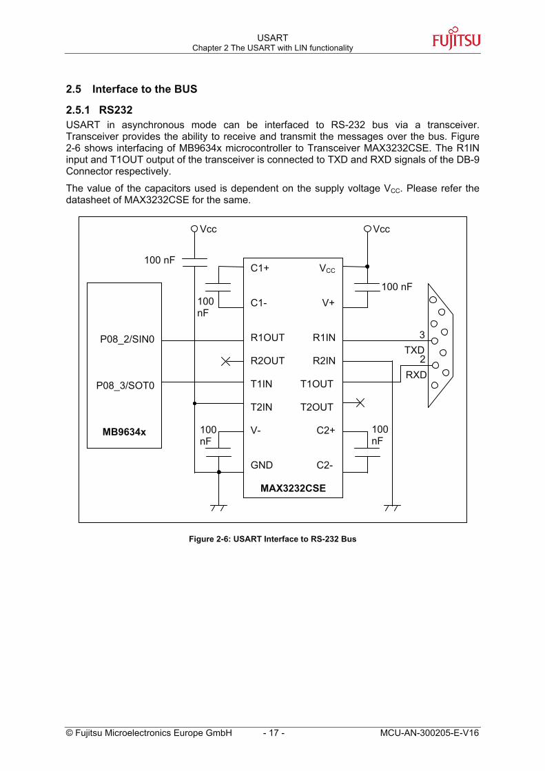
2.5 Interface to the BUS
2.5.1 RS232 USART in asynchronous mode can be interfaced to RS-232 bus via a transceiver. Transceiver provides the ability to receive and transmit the messages over the bus. Figure 2-6 shows interfacing of MB9634x microcontroller to Transceiver MAX3232CSE. The R1IN input and T1OUT output of the transceiver is connected to TXD and RXD signals of the DB-9 Connector respectively.
The value of the capacitors used is dependent on the supply voltage VCC. Please refer the datasheet of MAX3232CSE for the same.
Figure 2-6: USART Interface to RS-232 Bus
2
3
RXD
TXD
100 nF
Vcc
100 nF
100 nF
100 nF
100 nF
C1+ VCC
C1- V+
R1OUT R1IN R2OUT R2IN T1IN T1OUT T2IN T2OUT V- C2+
GND C2-
MAX3232CSE
P08_2/SIN0
P08_3/SOT0
MB9634x
Vcc
USART Chapter 2 The USART with LIN functionality
MCU-AN-300205-E-V16 - 18 - © Fujitsu Microelectronics Europe GmbH
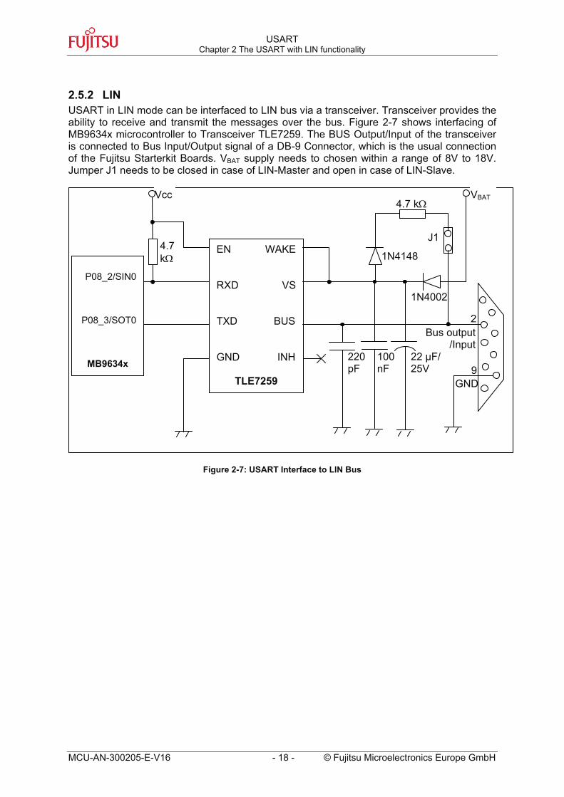
2.5.2 LIN USART in LIN mode can be interfaced to LIN bus via a transceiver. Transceiver provides the ability to receive and transmit the messages over the bus. Figure 2-7 shows interfacing of MB9634x microcontroller to Transceiver TLE7259. The BUS Output/Input of the transceiver is connected to Bus Input/Output signal of a DB-9 Connector, which is the usual connection of the Fujitsu Starterkit Boards. VBAT supply needs to chosen within a range of 8V to 18V. Jumper J1 needs to be closed in case of LIN-Master and open in case of LIN-Slave.
Figure 2-7: USART Interface to LIN Bus
9
2
GND
Bus output /Input
J1
1N4002
1N4148
4.7 kΩ
4.7 kΩ
22 µF/25V
100nF
220 pF
VBATVcc
EN WAKE
RXD VS
TXD BUS
GND INH
TLE7259
P08_2/SIN0
P08_3/SOT0
MB9634x
USART Chapter 2 The USART with LIN functionality
© Fujitsu Microelectronics Europe GmbH - 19 - MCU-AN-300205-E-V16
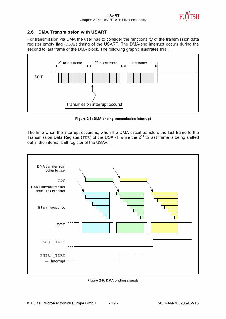
2.6 DMA Transmission with USART For transmission via DMA the user has to consider the functionality of the transmission data register empty flag (TDRE) timing of the USART. The DMA-end interrupt occurs during the second to last frame of the DMA block. The following graphic illustrates this:
Figure 2-8: DMA ending transmission interrupt
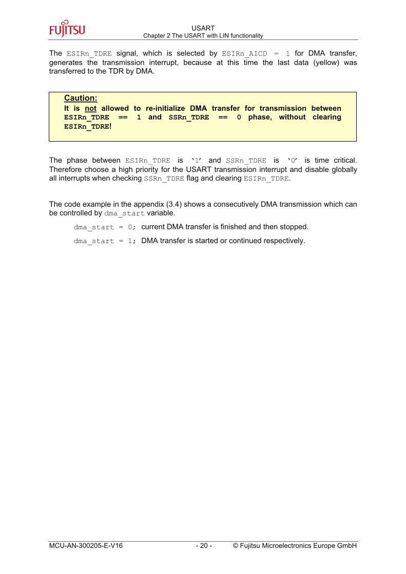
The time when the interrupt occurs is, when the DMA circuit transfers the last frame to the Transmission Data Register (TDR) of the USART while the 2nd to last frame is being shifted out in the internal shift register of the USART.
Figure 2-9: DMA ending signals
SOT
3rd to last frame 2nd to last frame last frame
Transmission interrupt occurs!
DMA transfer from buffer to TDR
TDRUART internal transfer
form TDR to shifter
Bit shift sequence
SOT
SSRn_TDRE
ESIRn_TDRE→ Interrupt
USART Chapter 2 The USART with LIN functionality
MCU-AN-300205-E-V16 - 20 - © Fujitsu Microelectronics Europe GmbH
The ESIRn_TDRE signal, which is selected by ESIRn_AICD = 1 for DMA transfer, generates the transmission interrupt, because at this time the last data (yellow) was transferred to the TDR by DMA.
The phase between ESIRn_TDRE is ‘1’ and SSRn_TDRE is ‘0’ is time critical. Therefore choose a high priority for the USART transmission interrupt and disable globally all interrupts when checking SSRn_TDRE flag and clearing ESIRn_TDRE.
The code example in the appendix (3.4) shows a consecutively DMA transmission which can be controlled by dma_start variable.
• dma_start = 0; current DMA transfer is finished and then stopped.
• dma_start = 1; DMA transfer is started or continued respectively.
Caution:It is not allowed to re-initialize DMA transfer for transmission between ESIRn_TDRE == 1 and SSRn_TDRE == 0 phase, without clearing ESIRn_TDRE!
USART Chapter 3 USART Examples
© Fujitsu Microelectronics Europe GmbH - 21 - MCU-AN-300205-E-V16
3 USART Examples
EXAMPLES FOR USART
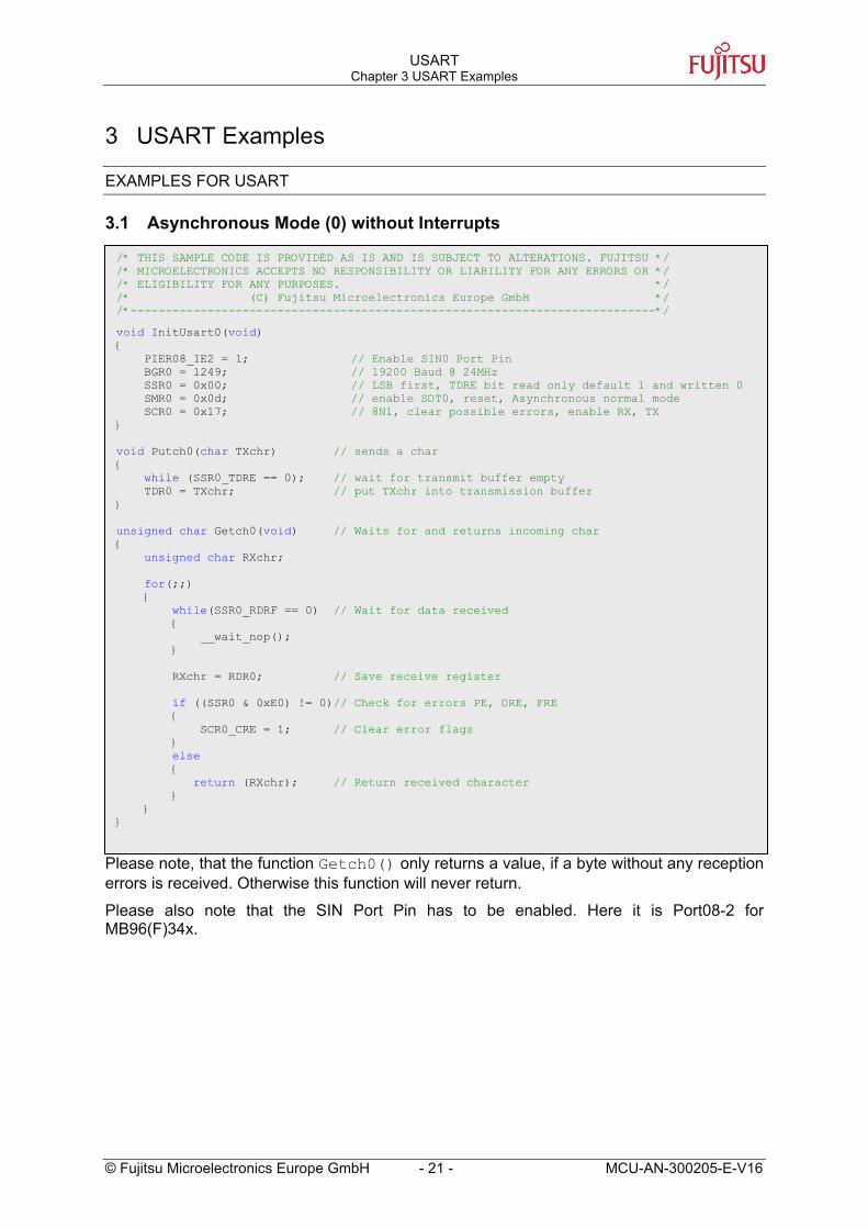
3.1 Asynchronous Mode (0) without Interrupts
Please note, that the function Getch0() only returns a value, if a byte without any reception errors is received. Otherwise this function will never return.
Please also note that the SIN Port Pin has to be enabled. Here it is Port08-2 for MB96(F)34x.
/* THIS SAMPLE CODE IS PROVIDED AS IS AND IS SUBJECT TO ALTERATIONS. FUJITSU */ /* MICROELECTRONICS ACCEPTS NO RESPONSIBILITY OR LIABILITY FOR ANY ERRORS OR */ /* ELIGIBILITY FOR ANY PURPOSES. */ /* (C) Fujitsu Microelectronics Europe GmbH */ /*---------------------------------------------------------------------------*/ void InitUsart0(void)
PIER08_IE2 = 1; // Enable SIN0 Port Pin BGR0 = 1249; // 19200 Baud @ 24MHz
SSR0 = 0x00; // LSB first, TDRE bit read only default 1 and written 0 SMR0 = 0x0d; // enable SOT0, reset, Asynchronous normal mode SCR0 = 0x17; // 8N1, clear possible errors, enable RX, TX
void Putch0(char TXchr) // sends a char
while (SSR0_TDRE == 0); // wait for transmit buffer empty TDR0 = TXchr; // put TXchr into transmission buffer
unsigned char Getch0(void) // Waits for and returns incoming char
unsigned char RXchr;
for(;;)
while(SSR0_RDRF == 0) // Wait for data received
__wait_nop();
RXchr = RDR0; // Save receive register
if ((SSR0 & 0xE0) != 0)// Check for errors PE, ORE, FRE
SCR0_CRE = 1; // Clear error flags else
return (RXchr); // Return received character
USART Chapter 3 USART Examples
MCU-AN-300205-E-V16 - 22 - © Fujitsu Microelectronics Europe GmbH
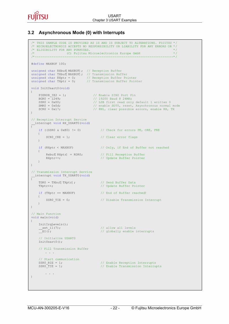
3.2 Asynchronous Mode (0) with Interrupts
/* THIS SAMPLE CODE IS PROVIDED AS IS AND IS SUBJECT TO ALTERATIONS. FUJITSU */ /* MICROELECTRONICS ACCEPTS NO RESPONSIBILITY OR LIABILITY FOR ANY ERRORS OR */ /* ELIGIBILITY FOR ANY PURPOSES. */ /* (C) Fujitsu Microelectronics Europe GmbH */ /*---------------------------------------------------------------------------*/ #define MAXBUF 100; unsigned char RXbuf[MAXBUF]; // Reception Buffer unsigned char TXbuf[MAXBUF]; // Transmission Buffer unsigned char RXptr = 0; // Reception Buffer Pointer unsigned char TXptr = 0; // Transmission Buffer Pointer void InitUsart0(void)
PIER08_IE2 = 1; // Enable SIN0 Port Pin BGR0 = 1249; // 19200 Baud @ 24MHz
SSR0 = 0x00; // LSB first read only default 1 written 0 SMR0 = 0x0d; // enable SOT0, reset, Asynchronous normal mode SCR0 = 0x17; // 8N1, clear possible errors, enable RX, TX
// Reception Interrupt Service __interrupt void RX_USART0(void)
if ((SSR0 & 0xE0) != 0) // Check for errors PE, ORE, FRE
SCR0_CRE = 1; // Clear error flags
if (RXptr < MAXBUF) // Only, if End of Buffer not reached
Rxbuf[RXptr] = RDR0; // Fill Reception Buffer RXptr++; // Update Buffer Pointer
// Transmission Interrupt Service __interrupt void TX_USART0(void)
TDR0 = TXbuf[TXptr]; // Send Buffer Data TXptr++; // Update Buffer Pointer
if (TXptr == MAXBUF) // End of Buffer reached?
SSR0_TIE = 0; // Disable Transmission Interrupt
// Main Function void main(void)
InitIrqLevels(); __set_il(7); // allow all levels __EI(); // globally enable interrupts
// Initialize USART0 InitUsart0();
// Fill Transmission Buffer . . .
// Start communication SSR0_RIE = 1; // Enable Reception Interrupts SSR0_TIE = 1; // Enable Transmission Interrupts
. . .
USART Chapter 3 USART Examples
© Fujitsu Microelectronics Europe GmbH - 23 - MCU-AN-300205-E-V16
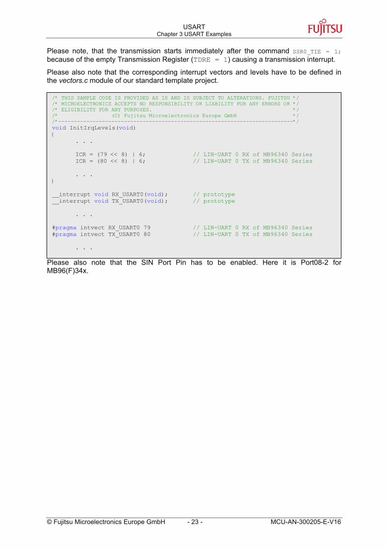
Please note, that the transmission starts immediately after the command SSR0_TIE = 1; because of the empty Transmission Register (TDRE = 1) causing a transmission interrupt.
Please also note that the corresponding interrupt vectors and levels have to be defined in the vectors.c module of our standard template project.
Please also note that the SIN Port Pin has to be enabled. Here it is Port08-2 for MB96(F)34x.
/* THIS SAMPLE CODE IS PROVIDED AS IS AND IS SUBJECT TO ALTERATIONS. FUJITSU */ /* MICROELECTRONICS ACCEPTS NO RESPONSIBILITY OR LIABILITY FOR ANY ERRORS OR */ /* ELIGIBILITY FOR ANY PURPOSES. */ /* (C) Fujitsu Microelectronics Europe GmbH */ /*---------------------------------------------------------------------------*/ void InitIrqLevels(void)
. . .
ICR = (79 << 8) | 6; // LIN-UART 0 RX of MB96340 Series ICR = (80 << 8) | 6; // LIN-UART 0 TX of MB96340 Series
. . .
__interrupt void RX_USART0(void); // prototype __interrupt void TX_USART0(void); // prototype
. . .
#pragma intvect RX_USART0 79 // LIN-UART 0 RX of MB96340 Series #pragma intvect TX_USART0 80 // LIN-UART 0 TX of MB96340 Series
. . .
USART Chapter 3 USART Examples
MCU-AN-300205-E-V16 - 24 - © Fujitsu Microelectronics Europe GmbH
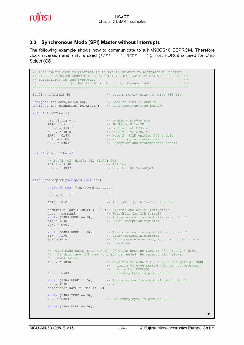
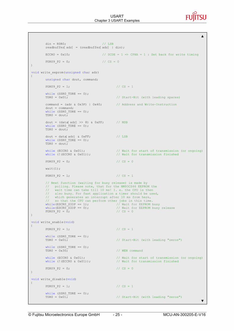
3.3 Synchronous Mode (SPI) Master without Interrupts The following example shows how to communicate to a NM93CS46 EEPROM. Therefore clock inversion and shift is used (SCES = 1, SCDE = 1). Port PDR09 is used for Chip Select (CS).
/* THIS SAMPLE CODE IS PROVIDED AS IS AND IS SUBJECT TO ALTERATIONS. FUJITSU */ /* MICROELECTRONICS ACCEPTS NO RESPONSIBILITY OR LIABILITY FOR ANY ERRORS OR */ /* ELIGIBILITY FOR ANY PURPOSES. */ /* (C) Fujitsu Microelectronics Europe GmbH */ /*---------------------------------------------------------------------------*/
#define DATASIZE 64 // eeprom memory size in words (16 Bit) unsigned int data[DATASIZE]; // Data to send to EEPROM unsigned int readbuffer[DATASIZE]; // Data received from EEPROM void InitUART(void)
PIER08_IE2 = 1; // Enable SIN Port Pin BGR0 = 15; // 1M Bit/s @ 16 MHz ESCR0 = 0x01; // SCES = 1 => CPOL = 1 ECCR0 = 0x10; // SCDE = 1 => CPHA = 1 SMR0 = 0x83; // Mode 2, SCLK enable, SOT enable SSR0 = 0x04; // MSB first, no interrupts SCR0 = 0x03; // Reception and transmission enable void InitPort09(void)
// Bit#2: CS, Bit#1: PE, Bit#0: PRE PDR09 = 0x00; // All Low DDR09 = 0x07; // CS, PE, PRE to output
void read_eeprom(unsigned char adr)
unsigned char din, command, dout;
PDR09_P2 = 1; // CS = 1
TDR0 = 0x01; // Start-Bit (with leading spaces)
command = (adr & 0x3F) | 0x80;// Address and Write-Instruction dout = command; // Swap Bits for MSB first??
while (SSR0_RDRF == 0); // Transmission finished (via reception)? din = RDR0; // Flush reception register TDR0 = dout;
while (SSR0_RDRF == 0); // Transmission finished (via reception)? din = RDR0; // Flush reception register SCR0_CRE = 1; // Clear possible errors, reset reception state
// machine
// NOTE: Make sure, that SCK is "0" while setting SCDE to "0" (ECCR0 = 0x00;) // In this case (1M bps) no check is needed. Be careful with slower // baud rates! ECCR0 = 0x00; // SCDE = 0 => CPHA = 0 : Needed for special read
// timing of used EEPROM (may be not necessary // for other EEPROM)
TDR0 = 0x00; // Set dummy byte to produce SCLK
while (SSR0_RDRF == 0); // Transmission finished (via reception)? din = RDR0; // MSB readbuffer[adr] = (din << 8);
while (SSR0_TDRE == 0); TDR0 = 0x00; // Set dummy byte to produce SCLK
while (SSR0_RDRF == 0);
USART Chapter 3 USART Examples
© Fujitsu Microelectronics Europe GmbH - 25 - MCU-AN-300205-E-V16
din = RDR0; // LSB
readbuffer[adr] = (readbuffer[adr] | din);
ECCR0 = 0x10; // SCDE = 1 => CPHA = 1 : Set back for write timing
PDR09_P2 = 0; // CS = 0
void write_eeprom(unsigned char adr)
unsigned char dout, command;
PDR09_P2 = 1; // CS = 1
while (SSR0_TDRE == 0); TDR0 = 0x01; // Start-Bit (with leading spaces)
command = (adr & 0x3F) | 0x40; // Address and Write-Instruction dout = command; while (SSR0_TDRE == 0); TDR0 = dout;
dout = (data[adr] >> 8) & 0xFF; // MSB while (SSR0_TDRE == 0); TDR0 = dout;
dout = data[adr] & 0xFF; // LSB while (SSR0_TDRE == 0); TDR0 = dout;
while (ECCR0 & 0x01); // Wait for start of transmission (or ongoing) while (!(ECCR0 & 0x01)); // Wait for transmission finished
PDR09_P2 = 0; // CS = 0
wait(1);
PDR09_P2 = 1; // CS = 1
// Next function (waiting for busy release) is made by
// polling. Please note, that for the NM93CS46 EEPROM the // wait time can take till 10 ms! I. e. the CPU is then // also busy. For fast application a timer should be used, // which generates an interrupt after 10 ms from here, // so that the CPU can perform other jobs in this time.
while(ESCR0_SIOP == 1); // Wait for EEPROM busy while(ESCR0_SIOP == 0); // Wait for EEPROM busy release PDR09_P2 = 0; // CS = 0
void write_enable(void)
PDR09_P2 = 1; // CS = 1
while (SSR0_TDRE == 0); TDR0 = 0x01; // Start-Bit (with leading "zeros")
while (SSR0_TDRE == 0); TDR0 = 0x30; // WEN command
while (ECCR0 & 0x01); // Wait for start of transmission (or ongoing) while (!(ECCR0 & 0x01)); // Wait for transmission finished
PDR09_P2 = 0; // CS = 0
void write_disable(void)
PDR09_P2 = 1; // CS = 1
while (SSR0_TDRE == 0); TDR0 = 0x01; // Start-Bit (with leading "zeros")
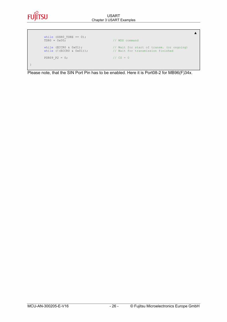
USART Chapter 3 USART Examples
MCU-AN-300205-E-V16 - 26 - © Fujitsu Microelectronics Europe GmbH
Please note, that the SIN Port Pin has to be enabled. Here it is Port08-2 for MB96(F)34x.
while (SSR0_TDRE == 0);
TDR0 = 0x00; // WDS command
while (ECCR0 & 0x01); // Wait for start of transm. (or ongoing) while (!(ECCR0 & 0x01)); // Wait for transmission finished
PDR09_P2 = 0; // CS = 0
USART Chapter 3 USART Examples
© Fujitsu Microelectronics Europe GmbH - 27 - MCU-AN-300205-E-V16
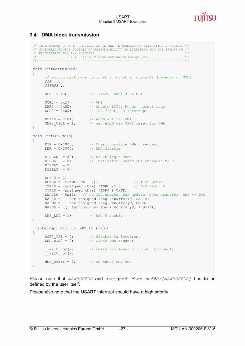
3.4 DMA block transmission
Please note that MAXBUFFER and unsigned char buffer[MAXBUFFER] has to be defined by the user itself.
Please also note that the USART interrupt should have a high priority.
/* THIS SAMPLE CODE IS PROVIDED AS IS AND IS SUBJECT TO ALTERATIONS. FUJITSU */ /* MICROELECTRONICS ACCEPTS NO RESPONSIBILITY OR LIABILITY FOR ANY ERRORS OR */ /* ELIGIBILITY FOR ANY PURPOSES. */ /* (C) Fujitsu Microelectronics Europe GmbH */ /*---------------------------------------------------------------------------*/
void InitUart0(void)
// switch port pins to input / output accordingly (depends on MCU) DDR ... PIER08 ...
BGR0 = 486; // 115200 Baud @ 56 MHz
SCR0 = 0x17; // 8N1SMR0 = 0x0D; // enable SOT0, Reset, normal mode
SSR0 = 0x00; // LSB first, no interrupt
ESIR0 = 0x01; // AICD = 1 for DMA SMR0_UPCL = 1; // set AICD via UART reset for DMA
void InitDMA(void)
DSR = 0x0000; // Clear possible DMA 0 request DER = 0x0000; // DMA disable
DISEL0 = 80; // UART0 irq number DISEL1 = 0; // Initialize unused DMA channels to 0 DISEL2 = 0; DISEL3 = 0;
DCTH0 = 0; DCTL0 = (MAXBUFFER - 1); // # of Bytes IOAH0 = (unsigned char) &TDR0 >> 8; // I/O Bank 00 IOAL0 = (unsigned char) &TDR0 & 0xFF; DMACS0 = 0x12; // no IOA update, BAP update, byte transfer, BAP -> IOA BAPH0 = (__far unsigned long) &buffer[0] >> 16; BAPM0 = (__far unsigned long) &buffer[0] >> 8; BAPL0 = ((__far unsigned long) &buffer[0] & 0xFF);
DER_EN0 = 1; // DMA 0 enable
__interrupt void IrqUART0tx (void)
SSR0_TIE = 0; // disable tx interrupt DSR_DTE0 = 0; // Clear DMA request
__wait_nop(); // delay for leaving ISR not too early __wait_nop();
dma_start = 0; // announce DMA end
USART Chapter 3 USART Examples
MCU-AN-300205-E-V16 - 28 - © Fujitsu Microelectronics Europe GmbH
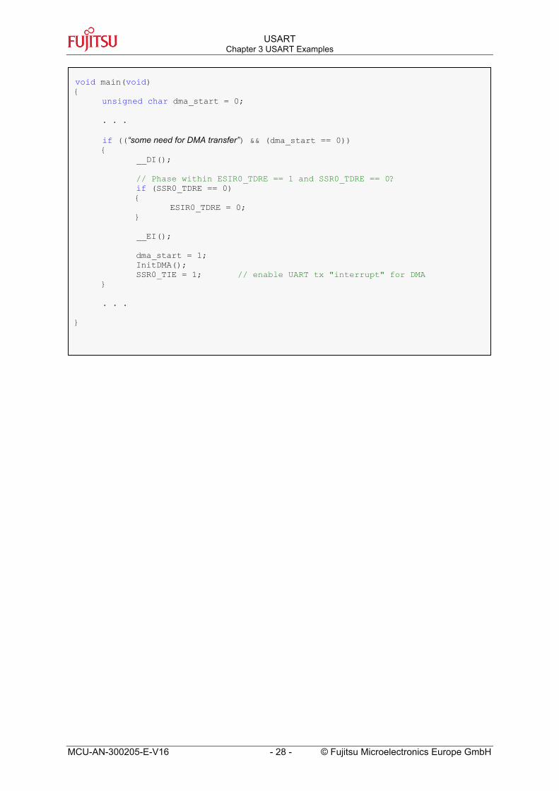
void main(void)
unsigned char dma_start = 0; . . .
if ((“some need for DMA transfer”) && (dma_start == 0)) __DI();
// Phase within ESIR0_TDRE == 1 and SSR0_TDRE == 0? if (SSR0_TDRE == 0)
ESIR0_TDRE = 0;
__EI();
dma_start = 1; InitDMA(); SSR0_TIE = 1; // enable UART tx "interrupt" for DMA
. . .
USART Chapter 4 APPENDIX A
© Fujitsu Microelectronics Europe GmbH - 29 - MCU-AN-300205-E-V16
4 APPENDIX A
RELATED DOCUMENTS
4.1 Related Documents Please find further information in the following documents.
• MCU-AN-390088-UART_LIN Usage of LIN-U(S)ART
• MCU-AN-390090-UART_LIN_BAUDRATE_CLK LIN-U(S)ART Baud Rate Generator
• MCU-AN-300002-SPI SPI Modes
• MCU-AN-390105-SPI_ADC SPI with MAX1286
• MCU-AN-390104-SPI_EEPROM SPI with NM93CS46
Note, that the above mentioned documents are written for 16LX MCUs, but also usable for 16FX-USART. Please also note that for 16FX devices the serial data or clock input port pin has to be enabled via PIER register.
USART Chapter 5 Additional Information
MCU-AN-300205-E-V16 - 30 - © Fujitsu Microelectronics Europe GmbH
5 Additional Information Information about FUJITSU Microcontrollers can be found on the following Internet page:
http://mcu.emea.fujitsu.com/
The software example related to this application note is:
96340_uart0_async
96340_uart0_async_interrupt
96340_uart1_async
96340_uart2_async
96340_uart3_async
96340_uart_lin_master
96340_uart_lin_slave
96340_uart_sync_spi_nm93cs46
96340_dma_uart0
It can be found on the following Internet page:
http://mcu.emea.fujitsu.com/mcu_product/mcu_all_software.htm
USART List of Figures
© Fujitsu Microelectronics Europe GmbH - 31 - MCU-AN-300205-E-V16
List of Figures Figure 2-1: USART Block Diagram .......................................................................................... 7 Figure 2-2: USART Clock ...................................................................................................... 13 Figure 2-3: CRE Bit Timing .................................................................................................... 14 Figure 2-4: De-synchronization Example............................................................................... 15 Figure 2-5: USART Dominant Bus Behaviour........................................................................ 16 Figure 2-6: USART Interface to RS-232 Bus ......................................................................... 17 Figure 2-7: USART Interface to LIN Bus................................................................................ 18 Figure 2-8: DMA ending transmission interrupt ..................................................................... 19 Figure 2-9: DMA ending signals............................................................................................. 19
USART List of Tables
MCU-AN-300205-E-V16 - 32 - © Fujitsu Microelectronics Europe GmbH
List of Tables Table 2-1: USART Operation Modes ....................................................................................... 8 Table 2-2: SCR ......................................................................................................................... 8 Table 2-3: SMR ......................................................................................................................... 9 Table 2-4: SSR ....................................................................................................................... 10 Table 2-5: ESCR ..................................................................................................................... 11 Table 2-6: ECCR ..................................................................................................................... 12 Table 2-7: Baud Rate corresponding to CLKP1..................................................................... 13