Embed Size (px)
Citation preview
FLOPPY/HARD DISK MANUAL

Specifications Subject to Change.
Convergent Technologies, Convergent, eTOS, CT-BUS, CT-DBMS, CT-MAIL, CT-Net, AWS, IWS, and NGEN are
trademarks of Convergent Technologies, Inc.
First Edition (January 1984) A-09-00328-01-A
Copyright © 1984 by Convergent Technologies, Inc.
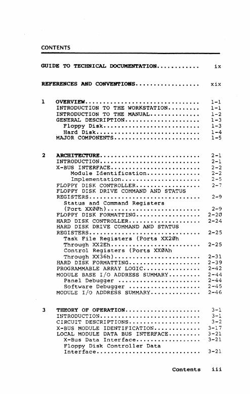
CONTENTS
GUIDE TO TECHNICAL DOCUMENTATION............ ix
REFERENCES AND CONVENTIOBS.................. xix
1
2
3
OVERVIEw ••••••••••••••.••••••••••••.•••• INTRODUCTION TO THE WORKSTATION ••••••••• INTRODUCTION TO THE MANUAL •••••••••••••• GENERAL DESCRIPTION •••••••••••••••••••••
Floppy Disk .....••.•.•.....•.......... Hard Disk ..•••.•.••.•••..•.•••........
MAJOR COMPONENTS ••••••••••••••••••••••••
ARCHI'l'EC'l'URE •••••••••••••••••••••••••••• INTRODUCTION •••••••••••••••••••••••••••• X-BUS INTERFACE •••••••••••••••••••••••••
Module Identification •••••••.••.••.• Implementation •••.•••••••••••••.••.•
FLOPPY DISK CONTROLLER •••••••••••••••••• FLOPPY DISK DRIVE COMMAND AND STATUS REGISTERS .••••••••••••••••••••••.••.••••
Status and Command Registers
1-1 1-1 1-2 1-3 1-3 1-4 1-5
2-1 2-1 2-2 2-2 2-5 2-7
2-9
(Port XX00h).......................... 2-9 FLOPPY DISK FORMATTING •••••••••••••••••• 2-20 HARD DISK CONTROLLER •••.•••••••••••••.•• 2-24 HARD DISK DRIVE COMMAND AND STATUS REGISTERS............................... 2-25
Task File Registers (Ports XX20h Through XX2Eh......................... 2-25 Control Registers (Ports XX0Ah Through XX36h)............... ••••••••• 2-31
HARD DISK FORMATTING •••••••••••••••.•.•• 2-39 PROGRAMMABLE ARRAY LOGIC ••••••••••••..•. 2-42 MODULE BASE I/O ADDRESS SUMMARy ••......• 2-44
Panel Debugger •••••••••••.••.•••••.•• 2-44 Software Debugger ••••••.•.••••..••••. 2-45
MODULE I/O ADDRESS SUMMARy ••••••••.••••• 2-46
THEORY OF OPERATION .••••.•••••••.•••••.• INTRODUCTION ••••••..•••.•••••••.•••..•.• C I RCU IT DESCRI PT IONS •••••••••••.•••••••. X-BUS MODULE IDENTIFICATION ••••••••.•••. LOCAL MODULE DATA BUS INTERFACE ••••••••.
X-Bus Dat'a Interface ••••••••••••.••••. Floppy Disk Controller Data Interface •••••••••••••••••••••••••••••
3-1 3-1 3-2
3-17 3-21 3-21
3-21
COntents iii
Hard Disk Controller Data Interface •••••••..•.•.••••••••••••••••
TRANSFER ACKNOWLEDGE GENERATION ••.•••••• FLOPPY/HARD DISK MODULE DEVICE DECODING ••••.••.••••••••••••.•••••••••.• FLOPPY DISK DRIVE CONTROLLER LOGIC •.••••
Introduction .•••••..•••••••.•••••••••• General Operation •..••••••••••.••••••• Floppy Disk Drive Clock Logic ••••.•.•• Floppy Disk Drive Interface Logic .•...
Control Signal s .•••••••••.•••• -•••••. Status Signals .••.•••.••••••••..••••
HARD DISK DRIVE CONTROLLER LOGIC •••••.•• Introduction •••••••••.•••••••••••••••. General Operation ••••••••••••••••.••••
DISABLE READ/WRITE ••••.••••••••••.•••••• Hard Disk Drive Clock Logic ••••••••••• Hard Disk Drive Interface Logic .•••.••
Control Signals •..•.••••••••.••••.•. Stepping Signals (Status) •••••••.••. Stepping Signals (Controls) ••.•.••••
HARD DISK DRIVE BOOT ROM •••••.••••••••.• HARD DISK DRIVE CONTROLLER RAM DATA BUFFER .•.••••.••••••••.••••.••.•.••••.•• RAM CHIP SELECTION AND ADDRESSING ....•.. RAM DATA DIRECTION ..••....•.••....••••.• DIRECT MEMORY ACCESS TRANSFERS ••..•••••. STATE SEQUENCER ••••....••••..••.•..•..•. HARD DISK DRIVE READ/WRITE CIRCUITRY •..••.•.•...•.••.••••••.••.••••
Read .•.•..•••....•.•.•.••••...•••.•••• MFM Data ••...•...••.•.•.••.•.....••. Phase-Detection Circuitry .•..•••.... Phase Synchronization •.•..••.•••.•..
Wr i te .•••••••.••••••••••...••••••••••. 8253 PROGRAMMABLE INTERVAL TIMERS ......•
Floppy Disk Operation ..•••••••.••••••• Hard Di sk Operation •••.••••..•.••.•.•.
POWER SUPPLIES .••.••••.••.•..••..••••••. FLOPPY/HARD DISK INTERCONNECT WIRE LIST •••.•••.••.•••.•....•••••.•..•. HARD DISK EXPANSION .•••.•.•.•••..••••.•• HARD DISK EXPANSION INTERCONNECT WIRE LIST •••..••••........•.••••...•...•
iv Floppy/Hard Disk Manual
3-22 3-24
3-24 3-27 3-27 3-35 3-36 3-36 3-37 3-39 3-40 3-40 3-45 3-46 3-47 3-47 3-48 3-50 3-51 3-52
3-52 3-55 3-57 3-58 3-63
3-66 3-66 3-66 3-67 3-68 3-69 3-70 3-70 3-75 3-80
3-81 3-86
3-3"7
APPEII1DIXES
APPENDIX A: FLOPPY/HARD DISK MODULE SPECIFICATION.................... A-I
APPENDIX B: MITSUBISHI MINI FLEXIBLE-DISK DRIVE - M4852/M4853 -SPECIFICATIONS. • • • • • • • • • • • • • • • . . . . • • • • • • B-1
APPENDIX C: TANDON RIGID DISK DRIVES - TM251, TM252................... C-I
GIDSSARY............................. Glossary-l
IlI1DBX. • • • • • • • • • • • • • • • • • • • • • • • • • • • • • • • • • • Index-l
Contents v
LIST OF FIGURES
Figure
l-I. 2-1.
2-2. 2-3. 2-4.
2-5.
Floppy/Hard Disk Module ••••••••••••••• Floppy/Hard Disk Module Functional Logic Block Diagram ••••••••••••••••••• Floppy Disk Track Format •••••••••••••• Hard Disk Track Format •••••••••••••••. 16L8 PAL Program for Integrated Circuit 7E ••••••.•••••••••••••••••••••• 16L8 PAL Program for Integrated
Page
1-3
2-3 2-21 2-41
2-43
Circuit 13E........................... 2-43 3-1. Floppy/Hard Disk Module Schematic
Diagram.................... ••••••••••• 3-3 3-2. Floppy Disk Controller Logic
Functional Block Diagram •••••••••••••• 3-33 3-3. Hard Disk Controller Logic
Functional Block Diagram •••••••••••••• 3-41 3-4. RAM Data Buffer Map ••••••••••••••••••• 3-53 3-5. Read/Write Sector Timing
Diagram. • • • • • • • • • • • • • • • • • • • • • • • • • • • • • • 3-59 3-6. Single Sector Read Timing
Diagram. • • • • • • • • • • • • • • • • • • • • • • • • • • • • • • 3-60 3-7. Single Sector Write Timing
Diagram. • • • • • • • • • • • • • • • • • • • • • • • • • • • • • • 3-61 3-8. State Sequencer Timing ••••.••••••••••• 3-63 3-9. Floppy Disk Controller
Programmable Interval Timer Logic Functional Block Diagram •••••••••••••• 3-71
3-10. Hard Disk Controller Programmable Interval Timer Logic Functional BloCK Diagram •••••••••••••• 3-78
vi Floppy/Hard Disk Manual
LIST OF TABLES
Table
2-1.
2-2.
2-3. 2-4. 2-5. 2-6. 3-1.
3-2.
3-3. 3-4.
3-5.
Floppy Disk Controller Command Summary ••••••••••••••••••••••• Floppy Disk Controller Flag Summary •••••••••••••••••••••••••• Status Register Summary ••••••••••••••• Floppy Disk Formatting Values ••••••••• Sample Sector Buffer ••••••••••• · ••.•••. I/O Address Summary •••••• , •••••••••••. WD2797-02 Floppy Disk Formatter/Controller Pin Assignments and Functions ••••••••••.•• WD10l0 Winchester Disk Controller Pin Assignments and Functions ••••••••• 6331-1 PROM Firmware Routine •••••••••• 8253 Programmable Interval Timer 4C Pin Assignments and Functions •••••••.• 8253 Programmable Interval Timer 5C Pin Assignments and Functions •..•.•••.
2-10
2-11 2-13 2-23 2-40 2-46
3-28
3-43 3-54
3-72
3-76
Contents vii

GUIDE TO TECHNICAL DOCUMENTATION
This manual is one of a set that documents the Convergent M Family of Information Processing Systems. The set can be grouped as follows:
Introductory Installation Guide Operator's Guide Executive Manual Context Manager Manual Status Codes Manual Installation Guide (NGEN) Operator's Guide (NGEN'
Hardware NGEN
Processor Manual: Model CP-OOl Dual Floppy Disk Manual Floppy/Hard Disk Manual Diagnostics Manual Keyboard Manual Power Syste~ Manual Monochrome Honi tor Manual: Ilode 1 VM-OOl Color Monitor Manual
IWS Workstation Hardware Manual Peripherals Hardware Manual IWS Peripherals Hardware Manual (SMD Version)
AWS Av-IS-2l0 Harnware Manual AWS-220, -230, -240 Hardware Hanual AWS Color Workstation Hardware Manual
Operating System CTOSM Operating System Manual System Programmer's Guide
Guest Operating Systems CP/M-86~ MSM-DOS (and GWM-BASIC) XENIX"
Programming Languages COBOL Manual FORTRAN Manual FORTRAN-R6 Manual BASIC Manual BASIC Compiler Manual Pascal Manual Assembly Language Manual
Documentation Guide ix
Program Development Tools COBOL Animator Editor Manual Debugger Manual Linker/Librarian Manual
Data Management Facilities CT-DBMS" Manual ISAM Manual Forms Manual Sort/Merge Manual
Text Management Facilities Word Processing User's Guide Word Processing Reference Manual Word Processing Quick Reference
Applications Facilities Project Planner Manual CT-MAIL" User's Reference Manual CT-MAIL" Administrator's Reference Manual Multiplan Business Graphics User's Guide Business Graphics Reference Manual Graphics Programmer's Guide Font Designer Manual
Communications Asynchronous Terminal Emulator Manual 3270 Terminal Emulator Manual 2780/3780 RJE Terminal Emulator Manual SNA Network Gateway Manual SNA 3270 Emulator Manual X.2S Network Gateway Manual Multimode Terminal Emulator User's Guide Multimode Terminal Emulator Reference Manual
This section outlines the contents of these manuals.
INTRODUCTORY
The Installation Guide describes the procedure for unpacking, cabling, and powering up a system.
The Operator's Guide addresses the needs of the average user for--Dperating instructions. It describes the workstation switches and controls, keyhoard function, and floppy disk handling.
x Floppy/Hard Disk Manual
; ...
The Executive Manual describes the command interpreter, the program that first interacts with the user when the system is turned on. It describes available commands and discusses command execution, file management, program invocation, and system management. It also addresses status inquiry, volume management, the printer spooler, and execution of batch jobs. This manual now incorporates the System Utilities and Batch Manuals.
The Context Manager Manual describes and teaches the use of the Context Manager, which allows the user to run applications concurrently and interchange them on the screen almost instantly.
The Status Codes Manual contains complete listings of all status codes, bootstrap ROM error codes, and CTOS initialization codes. The codes are listed numerically along with any message and an explanation.
The NGEN Installation Guide describes the procedure for unpacking, assembling, cabling, and powering up an NGEN workstation.
The NGEN Operator's Guide is a link between the operator, the NGEN workstation, and the workstation's documentation. The Operator's Guide
"describes the operator controls and the use of the floppy disk drives, as well as how to verify that the workstation is operational and how to use software release notices.
HARDWARE
NGEN
The Processor Manual: Model CP-OOl describes the Processor Module, which houses the Processor hoard, Memory board, I/O board, Video/Keyboard board, and Motherboard. It details the architecture and theory of operations of the printed circuit boards, external interfaces, and the Memory Expansion Cartridge, as well as the X-Bus specifications.
The Dual Floppy Disk Manual and the Floppy/Hard Disk Manual describe the architecture and theory of operation for the NGEN modules. They discuss the respective disk drives and controllers, and contain the applicable OEM disk drive manuals.
Documentation Guide xi
The Diagnostics Manual describes the diagnostics available for the NGEN workstation. It discusses the Processor Module' s bootstrap ROM program and error codes, and individual software diagnostics for modules in the workstation.
The Keyboard Manual describes the theory of operation for the NGEN keyboard.
The Power System Manual describes the operation and connections for the 36-Vol t Power Supply and the dc/dc converters used with the NGEN workstation.
The Monochrome Monitor Manual: Model VM-OOl describes the operation and connections of the 12-inch Monochrome Monitor used with the NGEN workstation.
The Color Monitor Manual describes the operation and conn.ections of the IS-inch Color Monitor used with the NGEN workstation.
IWS
The Workstation Hardware Manual describes the mainframe, keyboard, and video display for the IWS family of workstations. It specifies system architecture, printed circuit boards (Motherboard, Processor, I/O Memory, Multiline Communications Processor, Video Control, Graphics Control Board, ROM and RAM Expansions), keyboard, video monitor, Multibus interface, communications interfaces, power supply, and environmental characteristics of the workstation.
The Peripherals Hardware Manual describes the nonSMD single-board Mass Storage Subsystem (MSS) and Mass Storage Expansion (MSX) disk subsystems for the IWS family of workstations. It contains descriptions of the disk controller Motherboard, the two controller boards for floppy and Winchester disks, power supplies, disk drives, and environmental characteristics.
The IWS Peripherals Hardware Manual (SMD Version) describes the 5Mb MSS and MSX dis~ubsystems having one controller board.
xii Floppy/Hard Disk Manual
AWS
The AWS-210 Hardware Manual describes the mainframe, keyboard, and video display of the AWS-2l0 workstation. It specifies architecture, theory of operation of the printed circuit boards (Motherboard, Deflection, and CPU), keyboard, video monitor, expansion interface, cluster communications interface, power supply, and' environmental characteristics of the workstation.
The AWS-220, -230, -240 Hardware Manual describes the mainframe;--keyboard, disk controllers, and video display of the AWS-220, -230, and -240 workstations. It specifies architecture, theory of operation of the printed circuit boards (Motherboard, Deflection, 8088 CPU, 8086 CPU, Floppy Disk Controller, and Hard Disk Controller), keyboard, video monitor, cluster communications interface, external interfaces, power supply, and environmental characteristics of the workstation.
The AWS Color Workstation Hardware Manual describes the mainframe, keyboard, and color video display of the AWS Color Work.station. This manual reports the architecture and theory of operation of the printed circuit boards (Motherboard, Graphics Control Board, Hard Disk Controller, Color Video, Color Deflection, and CPU), keyboard, color monitor, peripheral interfaces, cluster communications interface, power supply, and environmental characteristics of the workstation. This manual also contains four OEM disk drive manuals and a summary of adjustments for the color monitor.
OPERATING SYSTEM
The CTOS" operating
Operating System Manual system. I~ specifies
describes services
the for
managing processes, messages, memory, exchanges, tasks, video, disk, keyboard, printer, timer, communications, and files. In particular, it specifies the standard file access methods: S&~, the sequential access methon; RSAM, the record sequential access method; and DAM, the direct access method.
Documentation Guide xiii
The System Programmer's Guide addresses the needs of the system programmer or system manager for detailed information on operating system structure and system operation. It describes (1) cluster architecture and operation, (2) procedures for building a customized operating system, and (3) diagnostics.
GUEST OPERATING SYSTEMS
The CP/M-86- and MS--DOS Manuals describe the single-user operating systems originally designed for the 8086-hased personal computer systems.
The GW--BASIC Manuals describe the version of BASIC that runs on the MS--DOS operating system.
The XENIX· Manuals describe the 16-bit adaptation of the UNIX system, including the XENIX environment for software development and text processing.
PROGRAMMING LANGUAGES
The COBOL, FORTRAN, FORTRAN-86, BASIC (Interpreterr;--BASIC Compiler, PASCAL, ~ Assembly Language l-1anua1s describe the system' s programming languages. Each manual specifies both the language itself and also operating instructions for that language.
The Pascal Manual is supplemented by a popular text, Pascal User Manual ~ Report.
The Assembly Language Manual is supplemented by a text, the Central Processing Unit, which describes the mal.n processor, the 8086. It specifies the machine architecture, instruction set, and programming at the symbolic instruction level.
PROGRAM DEVELOPMENT TOOLS
The COBOL Animator describes the COBOL Animator, a debugger that allows the user to interact directly wi th the COBOL source code during program execution.
The Editor Manual describes the text editor.
xiv Floppy/Bard Disk Manual
The Debugger Manual describes the Debugger, which is designed for use at the symbolic instruction level. It can be used in debugging FORTRAN, Pascal, and assembly-language programs. (COBOL and BASIC, in contrast, are more conveniently debugged using special facilities described in their respective manuals.)
The Linker/Librarian Manual describes the Linker, which links together separately compiled object files, and the Librarian, which builds and manages libraries of object modules.
DATA MANAGEMENT FACILITIES
The CT-DBMS· Manual describes Convergent's data base management system (CT-DBMS), which consists of (1) a data manipulation language for accessing and manipulating the data base and (2) utili ties for administering the data base acti~ities such as maintenance, backup and recovery, and status reporting.
The ISAM Manual describes both the single- and the mul tiuser indexed sequential access method. It specifies the procedural interfaces (and how to call them from various languages) and the utilities.
The Forms Manual describes the Forms facility that includes (1) the Forms Editor, which is used to interactively design and edit forms, and (2) the Forms run time, which is called from an application program to display forms and accept user input.
The Sort/Merge Manual describes (1) the Sort and Merge utilities that run as a subsystem invoked at the Executive command level, and (2) the Sort/Merge object mod\lles that can be called from an application program.
TEXT MANAGEMENT FACILITIES
The Word Processing User's Guide introduces the Word Processor to the first-time user. It provides step-by-step lessons that describe basic word processing operations. The lessons show how to execute operations and apply them to sample text.
Documentation Guide xv
The ~ Processing Reference Manual is a reference tool for users already familiar with the Word Processor. It describes the Word Processor keyboard and screen; basic, advanced, and programmer-specific operations; list processing; printer and print wheel configurations; and hardware considerations.
The Word Processing Quick Reference provides a concise summary of all word processing operations and briefly describes the keyboard and commands.
APPLICATIONS FACILITIES
The Project Planner schedules and analyzes tasks, milestones, and the allocation of resources in a project. By means of diagrams and several kinds of bar charts, Project Planner presents time and resource allocation results and shows the occurrence of project milestones. The Project Planner Hanual explains the use of the program and also serves as a reference once the user is fa~iliar with it.
The CT-MAIL'" User' s Reference Manual introduces the first-time user to the CT-MAIL electronic mail system. It provides step-by-step instructions for using the basic CT-MAIL operations to create, send, and receive mail.
The CT-~1AIL" Administrator' s Reference Manual provides the System Administrator with instructions for installing, configuring, and maintaining the CT-MAIL electronic mail system; setting up communication lines; creating and maintaining mail centers; adding mail users; creating distribution lists; and troubleshooting.
Multiplan is a financial modeling package designed for bus1ness planning, analysis, budgeting, and forecasting.
The Business Graphics User's Guide· introduces Business Graphics to the first-time user. It provides step-by-step lessons that describe basic Business Graphics operations. The lessons show how to execute operations and apply them to sample charts.
xvi Floppy/Hard Disk Manual
The Business Graphics Reference Manual is a reference tool for users already familiar with Business Graphics. It describes the Business Graphics keyboard and screen; box and arrow cursor movement; obtaining information from Multiplan; operations; and plotter configurations.
The Graphics Programmer's Guide is a reference for applications and systems programmers. It describes the graphics library procedures that can be called from application systems to generate graphic representations of data, and it includes a section on accessing Business Graphics from an application system.
The Font Designer Manual describes the interactive utility for designing new fonts (character sets) for the video display.
COMMUNICATIONS
The Asynchronous Terminal Emulator Manual describes the asynchronous terminal emulator.
The 3270 Terminal Emulator Manual describes the 3270 emulator package.
The 2780/3780 RJE Terminal Emulator Manual describes the 278073780 emulator package.
The SNA Network Gateway Manual describes the SNA Network Gateway, which supports data communications over an SNA network. The SNA Network Gateway comprises the Transport Service and Status Monitor. The Transport Service allows a Convergent workstation to function as cluster controller and forms the foundation for Convergent SNA products.
The SNA 3270 Emulator Manual describes the SPA 3270 emulator package. The SNA 3270 emulator provides CRT and printer subsystems in addition to a Virtual Terminal Interface for l:se in application programs.
The X.25 Network Gatpway Manual describes the X.25 Network Gateway, which supports CCITT Recommendation X.25 communications over a public data network. There are three levels of access to the network: packet, X.25 sequential access method,
Documentation Guide xvii
and the Mul timode Terminal communications option.
Emulator X.2S
The Multimode Terminal Emulator User's Guide introduces the Multimode Terminal Emulator to-tne first-time user. It describes the MTE video display, keyboard, display memory, and advanced operations for the X.2S communications option.
The Mul timode Terminal Emulator Reference Manual is a reference tool for sophisticated users of the Multimode Terminal Emulator. It describes the MTE escape sequences and field verification program.
CP/M-86 is a trademark of Digital Research.
MS, GW and XENIX are trademarks of Microsoft Corp.
UNIX is a trademark of Bell Laboratories.
xviii Floppy/Hard Disk Manual
REFERENCES AND CONVENTIONS
REFERENCES
The boards that make up the Floppy/Hard Disk Module are heavily dependent upon programmable large-scale integration (LSI) circuitry to perform their functions. Since hardware functions and software interfaces of the LSI circuitry are only summarized in this manual, users can find additional information in the following manufacturers' literature:
o Intel Component Data Catalog
o ~ Microprocessor ~ Peripheral Handbook
o Western Digital Cort>. WD10l0 Winchester Disk Controller data s~
o Western Digital Corp. WD279X-02 Floppy Disk Formatter/Controller Family data sheet
o Western Digital Corp. ~ Components Handbook
CONVENTIONS
NUMBERS
Numbers used in this manual are written in decimal unless suffixed with "h" for hexadecimal. For example, l0h = 16 and 0FFh = 255.
SIGNAL NAMES
Signal names used in this manual are suffixed with plus (+) and minus (-) to distinguish active-high from active-low, respectively. An example of a RD (Read) signal is as follows:
Sisnal Name Losical State Voltase Level
RD- 0 (active) Low 1 (inactive) High
RD+ 0 (inactive) Low 1 (active) High
References and Conventions xix
OVERVIEW
INTRODUCTION TO THE WORKSTATION
The workstation is composed of modules that provide data storage and processing functions. Depending on its configuration, the workstation will run application software as a standalone workstation, as a master workstation providing facilities for several cluster workstations, or as a cluster workstation.
In its most basic form, a workstation with Processor Module, Keyboard, and Monitor can run a software application as a cluster workstation. This configuration uses disk space on a cluster master to call up software applications and files. If disk storage is added, a workstation can store its own software applications and files. In this configuration, the workstation operates either as a standalone or provides disk storage services to cluster workstations as a cluster master.
Other modules, such as different or additional displays, processors, storage modules, communications modules, or keyboards, can be added to (or easily removed from) the workstation as processing needs change.
Since the workstation is modular, separate manuals provide details about logic, operation, and interface for the various modules of the system. The "Guide to Technical Documentation" in the front of this manual provides the complete list of manuals.
An explanation of the system capabilities and the system bus, designated as the X-Bus, is found in the Processor Manual for the system.
In this manual, the term "X-Bus master" is used to denote any device or module capable of accessing control of the X-Bus data, address, and control lines.
In sections describing the assignment of I/O base addresses, the term "Processor Module" is used. The Processor Module, itself an X-Bus master, is the only X-Bus master capable of assigning I/O base addresses to X-Bus modules during power-up reset, manual reset, or under software control.
Overview 1-1
INTRODUCTION TO THE MANUAL
This manual is written for the engineer who tests or services the Floppy/Hard Disk Module electronics or who writes or modifies system software for use with the workstation. This manual does not, however, support modifications to existing hardware. The manual is divided into the following sections:
o Overview
o Architecture
o Theory of Operation
o Hard Disk Expansion
The "Overview" describes Floppy/Hard Disk Module, components that make up Module.
the capabilities of the as well as the major the Floppy/Hard Disk
The second section, "Architecture," covers the floppy/hard disk controllers in terms of their applicable software interface to hardware components. Applicable command and status registers for the controllers, as well as other components, are defined. In addition, the X-Bus identification scheme is summarized.
Section 3, "Theory of Operation" details the component-level circuit descriptions of the Floppy/Hard Disk Module. In addition, an interconnect wire list is provided.
The subsection "Hard Disk Expansion," provides an interconnection wire list for a Hard Disk Expansion Module. In addition, module specifications and OEM manuals are provided in appendixes.
1-2 Floppy/Hard Disk Manual
GENERAL DESCRIPTION
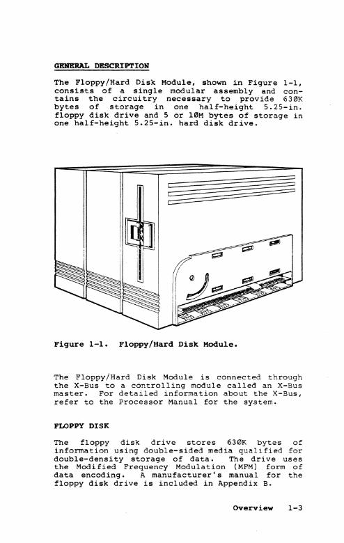
The Floppy/Hard Disk Module, shown in Figure 1-1. consists of a single modular assembly and contains the circuitry necessary to provide 630K bytes of storage in one half-height 5.25-in. floppy disk drive and 5 or 10M bytes of storage in one half-height 5.25-in. hard disk drive.
Figure 1-1. Floppy/Hard Disk Module.
The Floppy/Hard Disk Module is connected through the X-Bus to a controlling module called an X-Bus master. For detailed information about the X-Bus, refer to the Processor Manual for the system.
FLOPPY DISK
The floppy disk drive stores 630K bytes of information using double-sided media qualified for double-densi ty storage of data. The drive uses the Modified Frequency Modulation (MFM) form of data encoding. A manufacturer I s manual for the floppy disk drive is included in Appendix B.
OVerview 1-3
The floppy disk circuitry uses a 40-pin Western Digital WD2797-02 floppy' disk formatter I controller, which contains most of the logic necessary to control the floppy disk drive, including a phase-locked loop data separator, write precompensation circuitry, and cyclic redundancy checking (CRC) circuitry. In addition, an 8253 programmable interval timer supplements the WD2797-02.
HARD DISK
The hard disk drive stores SM or 10M bytes of information using Winchester technology. The drive uses the MFM form of data encoding.
The hard disk circuitry uses a 40-pin Western Digital WD1010 Winchester disk controller, which is used with an external 8K byte RAM data buffer. In addition, one 6331-1 PROM, two 8253 programmable interval timer chips, two 16L8 programmable array logic (PAL) 'chips, and phase-locked loop data separator circuitry supplement the WD1010.
1-4 Floppy/Hard Disk Manual
MAJOR COMPONENTS
The major components of the Floppy/Hard Disk Module include the following:
o the enclosure, which houses the drives, controllers, and X-Bus interface
o the motherboard, which lies agains.t the bottom of the enclosure
o the Controller board, which is mounted vertically along the left side of the enclosure
o two dc/dc power converters that plug into the motherboard, one supplying +12 Vdc and one supplying +5 Vdc
o one half-height floppy disk drive mounted vertically in the enclosure
o one half-height hard disk drive mounted vertically in the enclosure
Major components used for logic, which are resident on include the following:
o one WD2797-02 floppy disk
floppy disk control the Controller board,
formatter/controller
o one programmable interval timer (also used for the hard disk drive)
Major components used for hard disk control logic are resident on the Controller. board and include the following:
o one WD1010 Winchester disk controller
o two 8253 programmable interval timers (one of which is also used for the floppy disk controller)
o one 633,1-1 PROM
o two PAL chips
o four 2K by 8 bits (2K-byte) RAM chips
o one 4K by 8 bits (4K-byte) 2732 EPROM
o one MC4044 phase-frequency detector
o one 748124 voltage-controlled oscillator
Overview 1-5
2 ARCHITECTURE
INTRODUCTION
This section provides information for the systems programmer who needs to understand the Floppy/Hard Disk Module hardware at a functional block level and who must program the large-scale integration (LSI) devices within the Floppy/Hard Disk Module.
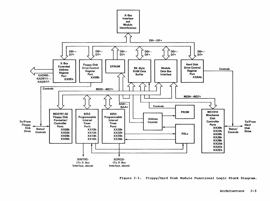
A functional logic block diagram is shown in Figure 2-1. Each block is described in this section in relation to the programmable LSI device or devices performing the applicable function in the workstation. Each subsection describes the nature of the function and how it is implemented. In addition, specific status and command registers are examined.
The following sUbjects are detailed:
o X-Bus interface
o floppy disk controller
o floppy disk command and status registers
o floppy disk formatting
o hard disk controller
o hard disk command and status registers
o hard disk formatting
o programmable array logiC
o module base input/output (I/O) addressing
o module I/O address summary
Architecture 2-1
X-8US INTERFACE
The I/O ports on the Floppy/Hard Disk Module are partially defined by the module base I/O address issued by the Processor Module. For example, the floppy disk Data register resides at port XX136h, where XX is the module address and 136h is the register address. Upon either a power-up or manual reset, the bootstrap ROM program in the Processor Module assigns a unique address to each module that is physically attached to the X-Bus. The operating system also has the ability to change module addresses at any time. Procedures used to change the module address through the operating system are, included in the "Module Base I/O Address Summary" subsection at the end of this section. In addition, a summary of I/O register addresses used with the Floppy/Hard Disk Module is provided in the "Module I/O Address Summary" subsection.
MODULE IDENTIFICATION
A power-up, manual reset, or any I/O operation to port 13F9813h resets all X-Bus modules, except the Processor Module. Only the module immediately to the right of the Processor Module is enabled. This module identifies itself by placing a type/state word on the data bus when port 13 is read by the Processor Module. (To reset the X-Bus modules via port 13F9813h, see the "Panel Debugger" subsection, below.)
The Processor Module writes to port 13 a base I/O address that corresponds to a register in the module (for example, the Floppy!Hard Disk Module) and defines the range of I/O addresses reserved for its use. Writing to port 13 also causes the module to reenable the X-Bus connection to the next module and to ignore subsequent reads and writes to and from port 13. This allows the Processor Module to repeat the process for each module, beginning at the module adjacent to the Processor Module and repeating the process for each module to the right.
A ready time-out, signaled by a nonmaskable interrupt (NMI) when accessing port 13, signifies that no additional modules are available.
2-2 Floppy/Bard Disk Manual
To!From Flopp
Dis Driv
y k e
X-Bus Interface
and Module
Identification
DO+-DF+
/"-. DO+- J l DO+- 1 [DO+- } 00'- 100.- J 00+-
'i '7 07+ "i '7 D7+ D7+ DF+ D7+ 'i 7 07+ "-..L ~ V
X-Bus Floppy Disk Hard Disk Extended Drive Control EPROM
8K-Byte Module Drive Control Controls Address Register RAM Data Data Bus Register Register Port /~ Buffer Interface Port XADRO-, Port XX08h XXOAh XAORll-- XXOEh
XADR17-J <~
Controls MDO+-MD7+ j'_t 4r 1 f
J WD2797-02 Floppy Disk Formatter! Controller
Ports Status! XXOOh
Controls XX02h XX04h XX06h
8253 Programmable
Interval Timer Ports
XX10h XX12h XX14h XX16h
XINTRS(To X-Bus
Interface, above)
I
~ BAA+
8253 Programmable
Jnterval Timer Ports
XX30h XX32h XX34h XX36h
XDRQ3-(To X-Bus
Interface, above)
I I I
I Controls
~ Address Counter
WDO+-WD7+
PROM
PALs
J J
~~ WD10l0
Winchester Disk
Controller Ports
XX20h XX22h XX24h XX26h XX28h XX2Ah XX2Ch XX2Eh
Status! Controls
To/From Hard Disk Drive
Figure 2-1. Floppy/Hard Disk Module Functional Logic Block Diagram.
Architecture 2-3
IMPLEMENTATION
The module identification scheme is implemented by hardware as follows:
o All modules on the X-Bus are assigned an input signal line (XPIN) and are required to generate an output signal line (XPOUT). The input signal will always enter a module on the module's left side, and the output signal will always exit the module on the module's right side. .
o During power up, all modules reset an internal flip-flop to drive XPOUT low.
o The XPIN line of the module closest to Processor Module is controlled by Processor Module, when XPIN is low, the register clears.
the the I/O
o When a module's XPIN is high and its XPOUT is low, the base I/O address is zero.
o The Processor Module reads port 0 to identify the peripheral (in this case, the Floppy/Hard Disk Module) and then writes a byte to the low-order eight bits of the data bus, which become the high-order eight bits of the device's I/O address range (256-byte ports or l28-word ports). This write also enables the XPOUT line in the module, which allows the next module on the right to undergo the same operation.
So that 8-bit devices are not required to scan the high-order byte of a port, the base I/O address is wri tten to the low-order byte of port 0. This corresponds to the high-order byte of the l6-bit base address, and defines a range of up to 256 port addresses reserved for that module's use.
The Processor Module is always referred to as module 0, and the first module to the right of the Processor Module is referred to as module 1, and so on. The bootstrap ROM always writes this module number to the low byte of port 0 when it performs the identification polling sequence. Therefore, the module to the right of the Processor Module uses I/O ports 0l00h through 0lFFh, the next module to the right uses ports 0200h through 02FFh, and so on, depending on how
Architecture 2-5
many modules are used. .The bootstrap ROM also builds an array of the module type/ state words returned by each module and stores this table in memory for the system.
2-6 Floppy/Bard Disk Manual
FLOPPY DISK CONTROLLER
The Western Digital WD2797-a2 formatter/controller performs the basic types of disk commands:
floppy following
disk four
o Control commands (Type 1 commands) include movement of the read/write head to a specified track on the floppy disk (seeks), track jumping (steps), and track a recalibration or restoration. Control commands never involve a data transfer.
o Read/write commands (Type 2 and Type 3 commands) include sector or entire track data transfers. The controller can also read the identification information from a floppy disk sector.
o The Force Interrupt command (Type 4 command) is issued by the X-Bus master t.o terminate a multiple-sector read/write command or to ensure controller operation after a control operation.
For control and read/write commands, the X-Bus master addresses the WD2797-a2 through the X-Bus address bus and then issues the command to the WD2797-a2 on the XDAT0- through XDAT7- (X-Bus Data Bus) lines. Depending on the command, other registers, such as the Track register and the Sector register, may be loaded with the appropriate information. Immediately after the WD2797-a2 receives the command, it sets the Busy (controller busy) bit in the Status register (that is, bit 0 at port XX0ah) and executes the command. With the exception of the Force Interrupt command (below), the X-Bus master should not attempt to write to any register in the WD2797-02 when the Busy bit is set. When a command is finished, the WD2797-02 interrupts the X-Bus master, using the XINTR5- (X-Bus Interrupt, Priority 5) line.
When the Read Sector command is issued, the WD2797-02 begins reading the specified sector and assembles the first byte read in the Data register. Simultaneously, the WD2797-02 sets the DRQ+ (Data Request) bit in the Status register (that is, bit 1 at port XX00h) and also sends DRQ+ back to the X-Bus master as XDRQ4- (X-Bus Data Request, Priority 4). The X-Bus master reads the WD2797-02 Data register at address XX06h for the
Architecture 2-7
byte. The WD2797-02 continues to assemble bytes in the Data register and requests service from the X-Bus master. When the last byte is read from the Data register in the WD2797-02, the 8253 programmable interval timer circuit sets the XINTR5- line to the X-Bus master. The X-Bus master responds with a Force Interrupt command to the WD2797-02 to stop execution of the read command.
A Write Sector command executes in the same manner.
Under software control, two count'!rs of the 8253 supplement the operation of the WD2797-02 when a read or write command is issued. During such commands, the WD2797-02 cannot terminate the command and request an X-Bus interrupt until it senses that five index marks have been detected. It takes about 1000 milliseconds for the floppy disk to make five revolutions, and the 8253 issues .the interrupt as soon as counters 0 and 1 time out.
Before loading the command in the WD2797-02, the X-Bus master loads two counters in the 8253. counter 0 is loaded with the total byte count, minus 2, of the transfer and is clocked every time the X-Bus master addresses the Data register. Counter 1 is loaded with a number to count an interval of about 140 microseconds so the WD2797-02 can compute the two CRC bytes in case a read error has occurred in the last sector. Counter 1 is clocked by a I-MHz oscillator. The logic is arranged so that both counters must time out before an interrupt request is issued to the X-Bus master.
When the X-Bus master senses the interrupt after a multiple-sector read operation, it sends the Force Interrupt command to the WD2797-02. This command, wpich can be loaded into the WD2797-02 Command register at any time, terminates any command in progress. Several flag bits in the Force Interrupt command byte can be set to specify the WD2797 -02 command interrupt conditions. (See the subsection, "Floppy Disk Drive Command and Status Registers," below.)
2-8 Floppy/Hard Disk Manual
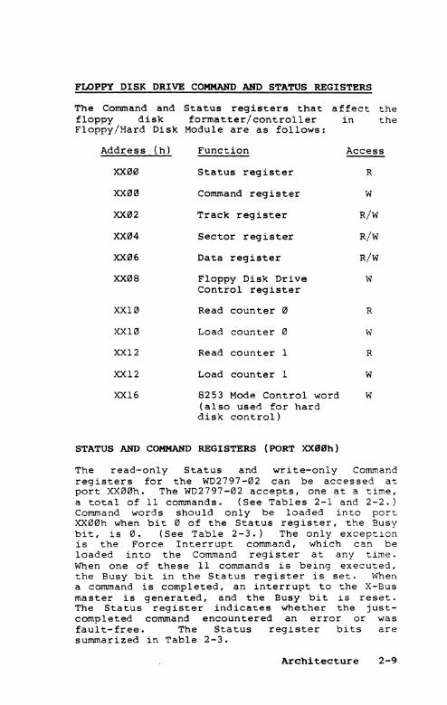
FLOPPY DISK DRIVE COMMAND AND STATUS REGISTERS
The Command and Status registers that affect the floppy disk formatter/controller in the Floppy/Hard Disk Module are as follows:
Address (h) Function Access
XX00 Status register R
XX00 Command register W
XX02 Track register R/W
XX04 Sector register R/W
XX06 Data register R/W
XX08 Floppy Disk Drive W Control register
XX10 Read counter 0 R
XX10 Load counter 0 W
XX12 Read counter 1 R
XX12 Load counter 1 W
XX16 8253 Mode Control word W ( also used for hard disk control)
STATUS AND COMMAND REGISTERS (PORT XX00h)
The read-only Status and write-only Command registers for the WD2797-02 can be accessed at port XX00h. The WD2797-02 accepts, one at a time, a total of 11 commands. (See Tables 2-1 and 2-2.) Command words should only be loaded into port XX00h when bit 0 of the Status register, the Busy bit, is 0. (See Table 2-3.) The only exception is the Force Interrupt command, which can be loaded into the Command register at any time. When one of these 11 commands is being executed, the Busy bit in the Status register is set. When a command is completed, an interrupt to the X-Bus master is generated, and the Busy bit is reset. The Status register indicates whether the justcompleted command encountered an error or was fault-free. The Status register bits are summarized in Table 2-3.
Architecture 2-9
Table 2-1- Floppy Disk Con1;roller ec..nand Su.aary.
~ Conunand* 7 6 5 4 3 2 1 " 1 Restore I?J I?J I?J I?J H V Rl R"
1 Seek I?J " " 1 H V Rl R"
1 Step I?J " 1 T H V Rl R"
1 Step-In I?J 1 I?J T H V Rl R"
1 Step-Out I?J 1 1 T H V Rl R"
2 Read Sector 1 I?J I?J M L E U " 2 Write Sector 1 " 1 M L E U A" 3 Read Address 1 1 I?J " " E U " 3 Read Track 1 1 1 " " E U 13
3 Write Track 1 1 1 1 " E U 13
4 Force Inter- 1 1 I?J 1 13 12 11 Ie rupt
*Refer to Table 2-2 for a description of the command parameters in this table
2-18 Floppy/Hard Disk Manual
Table 2-2. Floppy Disk Controller Flag Summary. (Page 1 of 2)
Command Type
1
2
2
Flag/Description
Rl, R0 = Stepping
motor rate
V Track number verify flag 0 No verify 1 = Verify on
destination track
H Head load flag
" Unload head at beginning
1 Load head at beginning
T Track update flag 0 No update 1 = Update track
register
L Sector length flag 0 = 256, 512, 1024,
and 128 for LSB's sector length in ID fields 00, 01, 10, and II, respectively
1 128, 256, 512, and 1024 for LSB's sector length in ID fields 00, 01, 10, and 11, respectively
M Multiple record flag 0 Single record 1 = Multiple records
Suggested Value
R0 and Rl = 0
V 0
H 0
T
L 1
command dependent
Architecture 2-11
Table 2-2. Floppy Disk Controller Flag Summary. (Page 2 of 2)
Command Type
2, 3
2, 3
2, 3
4
Flaq/Description
A0 = Data address mark o = FBh (DAM) I = F8h (deleted DAM)
U = Update SSO
E
IX
10
Il
12 13
o = Update SSO to 0 1 = Update SSO to 1
15 millisecond delay o No 15 millisecond
delay 1 15 millisecond
delay (30 millisecond for 1 MHz)
Interrupt condition flags 1 Not ready to ready transition 1 Ready to not ready transition 1 Index pulse 1 Immediate interrupt, requires reset
13- .. 10 = 0 Terminate with
no interrupt (INTRQ)
2-12 F1oppy/Bard Disk Manual
Suqgested Value
A0 o
command dependent
E 1
command dependent
Table 2-3. Status Register S-.ry. (Page 1 of 3)
Sw.aary of ec-ands
All Type I Read Read Read Write Wri'te
ill Commands Address ~ ~ ~ ~
" Busy Busy Busy Busy Busy Busy
1 Index Pulse ORO ORO ORO ORO ORO
2 Track "" Lost Lost Lost Lost Lost Data Data Data Data Data
3 CRC Error CRC Error CRC Error " CRe Error " 4 Seek Error RNF RNF " RNF eJ
5 Head Loaded eJ Record " eJ " Type
6 Write " " eJ Write Write Protect Protect Pro-
tect
7 Not Not Not Not Not Not Ready Ready Ready Ready Ready Ready
Architecture 2-13
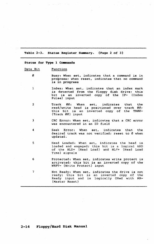
Table 2-3. Status Register SUllllllary. (Page 2 of 3)
Status for Type 1 Commands
Data Bit
1
2
3
4
5
6
7
Function
Busy: When set, indicates that a command is in progress~ when reset, indicates that no command is in progress
Index: When set, indicates that an index mark is detected from the floppy disk drive~ this bit is an inverted copy of the IP- (Index Pulse) input
Track 00: When read/wri te head this bit is an (Track 00) input
set, indicates is positioned over
inverted copy of
that the track 00~ the TR00-
eRe Error: When set, indicates that a eRe error was encountered in an 10 field
Seek Error: When set, indicates that the desired track was not verified~ reset to 0 when updated.
Head Loaded: When set, indicates the head is loaded and engaged~ this bit is a logical ANO of the HLO+ (Head Load) and HLr+ (Head Load Time) signals
Protected: When set, indicates write protect is activated~ this bit is an inverted copy of the WRPT- (Write Protect) input
Not Ready: When set, readY1 this bit is Ready input and is (Master Reset)
indicates the drive is not an inverted copy of the logically ORed with MR-
2-14 Floppy/Hard Disk Manual
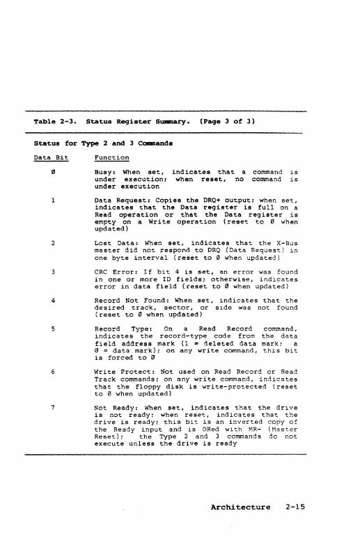
Table 2-3. Status Register SUllllllary. (Page 3 of 3)
Status for Type 2 and 3 Commands
Data Bit
Iil
1
2
3
4
5
6
7
Function
Busy. When set, indicates that a command is under execution; when reset, no command is under execution
Data Request. Copies the DRQ+ output; when set, indicates that the Data register is full on a Read operation or that the Data register is empty on a Write operation (reset to Iil when updated)
Lost Data. When set, indicates that the X-Bus master did not respond to DRO (Data Request) ~n one byte interval (reset to " when updated)
CRC Error. If bit 4 is set, an error was found in one or more ID fields; otherwise, indicates error in data field (reset to Iil when updated)
Record Not Found. When set, indicates that the desired track, sector, or side was not found (reset to " when updated)
Record Type. On a Read Record indicates the record-type code from field address mark (1 = deleted data " = data mark); on any write command, is forced to "
command, the data mark: a this bit
Write Protect. Not used on Read Record or Read Track commands; on any write command, indicates that the floppy disk is write-protected (reset to " when updated)
Not Ready. When set, indicates that the drive is not ready; when reset, indicates that the drive is ready; this bit is an inverted copy of the Ready input and is ORed with MR- (Master Reset): the Type 2 and 3 commands do not execute unless the drive is ready
Architecture 2-15
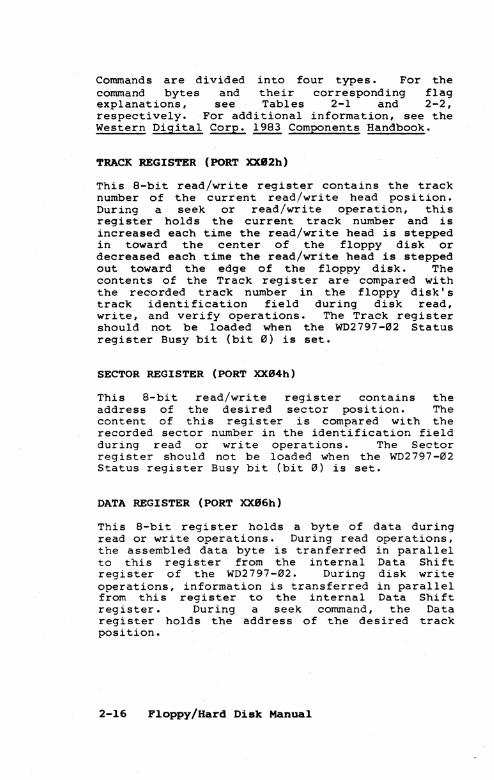
Commands are divided into four types. For the command bytes and their corresponding flag explanations, see Tables 2-1 and 2-2, respectively. For additional information, see the Western Digital Corp. 1983 Components Handbook.
TRACK REGISTER (PORT XXB2b)
This 8-bit read/write register contains the track number of the current read/write head position. During a seek or read/write operation, this register holds the current track number and is increased each time the read/write bead is stepped in toward the center of the floppy disk or decreased each time the read/write head is stepped out toward the edge of the floppy disk. The contents of the Track register .are compared with the recorded track number in the floppy disk IS
track identification field during disk read, write, and verify operations. The Track register should not be loaded when the WD2797-02 Status register Busy bit (bit 0) is set.
SECTOR REGISTER (PORT XX04h)
This 8-bit read/write register contains the address of the desired sector position. The content of this register is compared with the recorded sector number in the identification field during read or write operations. The Sector register should not be loaded when the WD2797-02 Status register Busy bit (bit 0) is set.
DATA REGISTER (PORT XXB6h)
This 8-bit register holds a byte of data during read or write operations. During read operations, the assembled data byte is tranferred in parallel to this register from the internal Data Shift register of the WD2797-02. During disk write operations, information is transferred in parallel from this register to the internal Data Shift register. During a seek command, the Data register holds the address of the desired track position.
2-16 Floppy/Hard Disk Manual
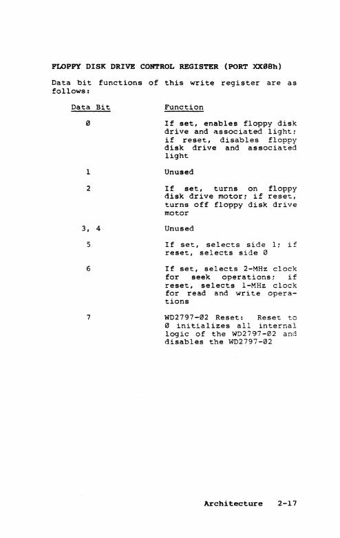
FLOPPY DISK DRIVE CONTROL REGISTER (PORT XX:08h)
Data bit functions of this write register are as follows:
Data Bit
1
2
3, 4
5
6
7
Function
If set, enables floppy disk drive and associated light; if reset, disables floppy disk drive and associated light
Unused
If set, turns on floppy disk drive motor; if reset, turns off floppy disk drive motor
Unused
If set, selects side I; if reset, selects side 0
If set, selects 2-MHz clock for seek operations; if reset, selects I-MHz clock for read and write operations
WD2797-02 Reset: Reset to o initializes all internal logic of the WD2797-02 and disables the WD2797-02
Architecture 2-17
COUNTER 13 (PORT XXIBh)
After the 8253 Mode Control word is written, two bytes are written into this register. counter 0 is clocked every time the X-Bus master addresses the WD2797-02 Data register. Counter 0 is loaded with two bytes to indicate the actual number of bytes to be transferred, minus 2, during the read or write operation. If, for example, a transfer involves 16 sectors of 256 bytes each, the hexadecimal equivalent of 4094 (0FFEh) is loaded into this register as follows:
1. Write FEh to port XX10h (least significant byte) •
2. Write 0Fh to port XX10h (most significant byte) •
COUNTER 1 REGISTER (PORT XX12h)
After the 8253 Mode Control word is written, two divisor bytes are written into this Counter register. The counter divides a I-MHz input clock by the number selected by the divisor bytes. This counter is programmed to time out about 140 microseconds after the data transfer to give the WD2797-02 enough time to compute the two CRC bytes in case of a read error. If, for example, a 140-microsecond timeout interval occurs, the hexadecimal equivalent of 140 (008Ch) is loaded into this register as follows:
1. Write 8Ch to port XX12h (least significant byte of the count).
2. Write 00 to port XX12h (most significant byte of the count).
2-18 Floppy/Hard Disk Manual
MODE CONTROL REGISTER (PORT XX16h)
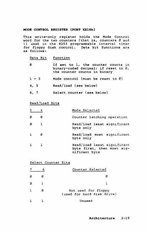
This write-only register holds the Mode Control word for the two counters (that is, counters 0 and 1) used in the 8253 programmable interval timer for floppy disk control. Data bit functions are as follows:
Data Bit
1 - 3
4, 5
6, 7
Function
If set to 1, the counter counts in binary-coded decimal; if reset to 0, the counter counts in binary
Mode control (must be reset to 0)
Read/load (see below)
Select counter (see below)
Read/Load Bits
5 4
1
1 '" 1 1
Select Counter Bits
7 6
'" '" '" 1
Mode Selected
counter latching operation
Read/load least significant byte only
Read/load most significant byte only
Read/load least significant byte first, then most significant byte
Counter Selected
'" 1
1 '"
Not used for floppy ( used for hard disk drive)
1 1 Unused
Architecture 2-19
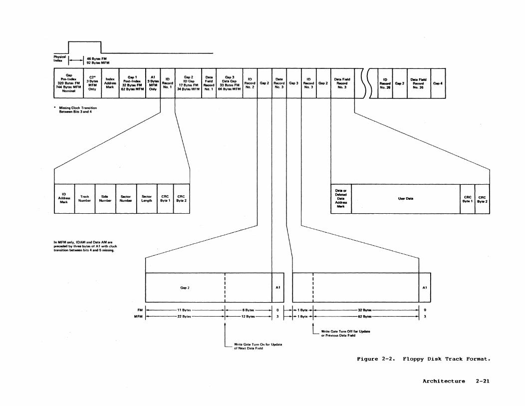
FLOPPY DISK FORMATTING
When the WD2797-02 formats a track on the floppy disk drive, the data for the formatting operation must be stored in the X-Bus master's memory. Formatting the floppy track is accomplished by posi tioning the read/write head over the desired track and issuing a Write Track command.
Upon receipt of the Write Track command, the read/write head is loaded, and the Busy bit (bit 0) is set. Writing starts with the leading edge of the first encountered index pulse and continues until the next index pulse, at which time the interrupt to the X-Bus master is asserted. The Data Request line is activated immediately upon receipt of the command, but writing does not start until after the first byte is loaded into the Data register. If the Data register has not been loaded by the time the index pulse is encountered, the operation is terminated (making the device Not Busy), the Lost Data staCtus bit (bit 2) is set, and the interrupt is asserted. If the operation starts, (that is, a first byte is written but a succeeding byte is not present in the Data register when needed), a byte of zeros is substituted.
This sequence continues from one index mark to the next. Normally, the data pattern appearing in the Data register is written on the disk with a normal clock pattern. If, however, the WD2797-02 detects a data pattern of F5h through FEh in the Data register, the WD2797-02 interprets this pattern as data address marks with missing clocks or CRC generation. As a consequence, F5h through FEh should not appear in the gap, data fields, or ID fields.
The CRC generator is initialized when any data byte from FBh to FEh is about to be transferred from the Data register to the internal Data Shift register or by receipt of F5h. An F7h pattern transferred from the Data register to the Data Shift register generates two CRC characters in MFM. CRCs must be generated by an F7h pattern.
The formatting values in hexadecimal for a floppy disk with 16 sectors of 256 bytes each are listed in Table 2-4. A drawing of the same floppy disk format is shown in Figure 2-2.
Floppy/Hard Disk Manual
~ Physicol I I Index ...-....... 46 Byt .. FM
92 Bytes MFM
GoP C2' Pre-Index Index 320 Bytes FM 3 Byt .. Address
MFM 744 Bytes MFM Only
M .. k Nominal
. Missing Clock Transition Between Sits 3 and 4
10 Track Side Address
Mark Number Number
In MFM only. lOAM and Data AM are preceded by three bytes of A 1 with clock transition between bits 4 and 5 m;ssi"t--
G ... l Al Gap 2 Data Gop 3
~~ 10 10 Data 10 Data Field 10 Data Field POit-lndex 3Byt .. Record 10 Gap Field DIU Gap Record Gap2 Record Gap 3 Retord Gap 2 Record Record G ... 2 Record 32Byt .. FM MFM 17 Byt .. FM Record 33 Bytes FM 62 BytesMFM Only No.1 34 By til MFM No.1 66 BY'IIMFM
No.2 No.3 No.3 No.3 No. 28 No. 26
Data or
Sect.,.. Sector CRC CRC DaI_
Da •• User O.ta Number length Byte 1 Byt.2 _III _k
I I I I
Gap 2 I Al I Al I I I I L
FM I.' II By'" "1-6 Bytes ---l 0 ~I-' Byte --I : 32 Bytes : 1 0 MFM "-~-----22 Bytes --------<.~1-12 8 YI8.-1 ~ --1 Byte ... ... >---------62 Bytes---------J-·
L~,.-'"-~., ...... of Next Oata Field
L Writ. G ... Turn 011 lor Update or Previous Oat. Field
Gap.
CRC CRC 8yto t Byte 2
Figure 2-2. Floppy Disk Track Format.
Architecture 2-21
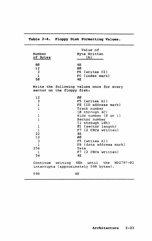
Table 2-4. Floppy Disk Formatting Values.
Number of Bytes
8e 12
3 1
5e
Value of Byte Written
(h)
4E ee F6 (writes C2) FC (index mark) 4E
Write the following values once for every sector on the floppy disk:
12 00 3 F5 (writes Al) 1 FE (1D address mark) 1 Track number
(e thrnugh 4C) 1 Side number (0 or 1) 1 Sector number
(1 through l0h) 1 el (sector length) 1 F7 (2 CRCs written)
22 4E 12 ee
3 F5 (writes Al) 1 FB (data address mark)
256 Data 1 F7 (2 CRCs written)
54 4E
Continue writing 4Eh until the WD2797-02 interrupts (approximately 598 bytes).
598 4E
Architecture 2-23
HARD DISK CONTROLLER
A disk operation begins when the X-Bus master wri tes task information into the Task File registers of the WD10l0 Winchester disk controller. The task information includes the disk cylinder number, head number, sector number, drive number, track number for start of write precompensation, sector size, and the number of sectors to be transferred. After the task information has been written, the X-Bus master writes the command into the Command register. During a Write Sector command, the X-Bus master reads the status of the WD10l0 to inspect the buffer data request flag, and then writes data into the RAM data buffer.
When the RAM data buffer is full, the BRDY+ (Buffer Ready) input of the WDl0l0 is activated. Then. the WD10l0 de-asserts the BDRQ+ (Buffer Data Request) line and asserts BCS- (Buffer Chip Select).
The buffered data is transferred to the hard disk, and the RAM data buffer becomes empty.
2-24 Floppy/Hard Disk Manual
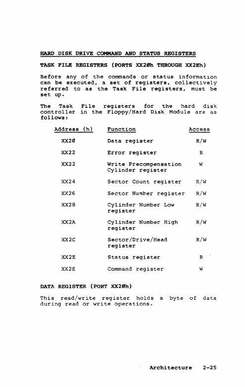
HARD DISK DRIVE COMMAND AND STATUS REGISTERS
TASK FILE REGISTERS (PORTS XX2Sh THROUGH XX2Eh)
Before any of the commands or status information can be executed, a set of registers, collectively referred to as the Task File registers, must be set up.
The Task controller follows:
File registers for the hard disk in the Floppy/Hard Disk Module are as
Address (h) Function Access
XX211J Data register R/W
XX22 Error register R
XX22 Write Precompensation W Cylinder register
XX24 Sector Count register R/W
XX26 Sector Nu~ner register R/W
XX28 Cylinder Number Low R/W register
XX2A Cylinder Number High R/W register
XX2C Sector/Drive/Head R/W register
XX2E Status register R
XX2E Command register W
DATA REGISTER (PORT XX2Sh)
This read/write register holds a byte of data during read or write operations.
Architecture 2-25
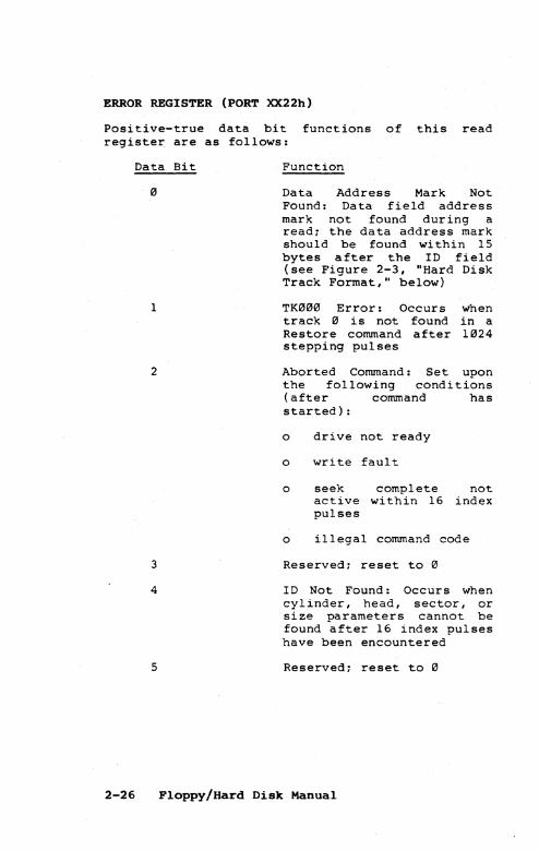
ERROR REGISTER (PORT XX22h)
Positive-true data bit functions of this read register are as follows:
Data Bit
1
2
3
Function
Data Address Mark Not Found: Data field address mark not found during a read~ the data address mark should be found within 15 bytes after the ID field (see Figure 2-3, "Hard Disk Track Format," below)
TK000 Error: Occurs when track 0 is not found in a Restore command after 1024 stepping pulses
Aborted Command: Set upon the following conditions (after command has started) :
0 drive not ready
0 write fault
0 seek complete not active within 16 index pulses
0 illegal cOllUlland code
Reserved~ reset to 0
4 ID Not Found: Occurs when cyl inder I head, sector, or size parameters cannot be found after 16 index pulses have been encountered
5 Reserved~ reset to 0
2-26 Floppy/Hard Disk Manual
6
7
Data Field CRC: Error detected in the data field; the sector can be reread to attempt recovery from a soft error (the data contained in the buffer can be read, but contains errors)
Bad Block: A bad block address mark has been detected during read or write attempt
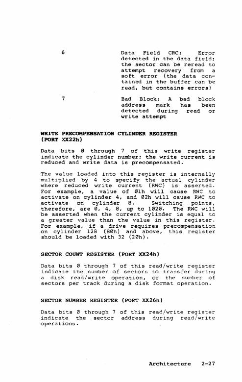
WRITE PRECOMPEJISATION CYLINDER REGISTER (PORT XX22h)
Data bits 0 through 7 of this write register indicate the cylinder number; the write current is reduced and write data is precompensated.
The value loaded into this register is internally multiplied by 4 to specify the actual cylinder where reduced write current (RWC) is asserted. For example, a value of 01h will cause RWC to activate on cylinder 4, and 02h will cause RWC to activate on cylinder B. Switching points, therefore, are 0, 4. B, up to 1020. The RWC will be asserted when the current cylinder is equal to a greater value than the value in this register. For example, if a drive requires precompensation on cylinder 12B (80h) and above, this register should be loaded with 32 (20h).
SECTOR COUNT REGISTER (PORT XX24h)
Data bits '" through 7 of this read/write register indicate the number of sectors to transfer during a disk read/write operation, or the number of sectors per track during a disk format operation.
SECTOR NUMBER REGISTER (PORT XX26h)
Data bits '" through 7 of this read/write register indicate the sector address during read/write operations.
Architecture 2-27
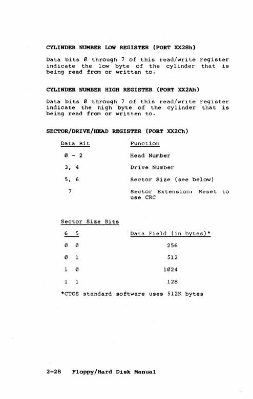
CYLINDER NUMBER LOW REGISTER (PORT XX28h)
Data bits ~ through 7 of this read/write register indicate the low byte of the cylinder that is being read from or written to.
CYLINDER NUMBER HIGH REGISTER (PORT XX2Ah)
Data bits ~ through 7 of this read/write register indicate the high byte of the cylinder that is being read from or written to.
SECTOR/DRIVE/HEAD REGISTER (PORT XX2Ch)
Data Bit Function
~ - 2 Head Number
3, 4 Drive Number
5, 6 Sector Size (see below)
7 Sector Extension: Reset to use CRC
Sector Size Bits
6 5 Data Field (in bJ::tes)*
0 ~ 256
~ 1 512
1 0 1~24
1 1 128
*CTOS standard software uses 5l2K bytes
2-28 Floppy/Hard Disk Manual
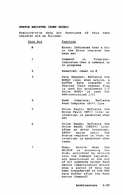
STATUS REGISTER (PORT XX2Eh)
Positive-true data bit functions of this read register are as follows:
Data Bit
1
2
3
4
5
6
7
Function
Error: Indicates that a bit in the Error register has been set·
Command in Progress: Indicates that a command is in progress
Reserved: reset to 0
Data Request: Reflects the BDRQ+ line: when active, a buffer data transfer is desired (Data request flag is used for programmed I/O while BDRQ+ is used for DMA-controlled I/O)
Seek Complete: Reflects Seek Complete (SC+) line
Write Fault: Reflects the Write Fault (WF+) line; an interrupt is generated when set
Drive Ready: Reflects the Drive Ready (DRDY+) line; after an error interrupt, DRDY+ waits until the Status register is read: an interrupt is generated when reset
Busy: Active when the WDll2JII2J is accessing the disk; activated by writing into the Command register, and deactivated at the end of all commands except Read Sector (deactivation occurs when a sector of data has been transferred to the RAM data buffer after the Read Sector Command)
Architecture 2-29
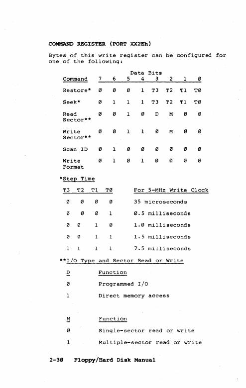
COMMAND REGISTER (PORT X:X2Eh)
Bytes of this write register can be configured one of the following:
Command 7 6 5
Restore* 0 0 0
Seek* 0 1 1
Read 0 0 1 Sector**
Write 0 0 1 Sector**
Scan ID 0 1
Write 0 1 Format
*SteE Time
Data 4
1
1
0
1
o
1
Bits 3
T3
T3
D
0
2 1 0
T2 Tl T0
T2 Tl T0
M 0 0
M 0 0
T3 T2 Tl T0 For 5-MHz Write Clock
0 0 0 0 35 microseconds
0 0 0 1 0.5 milliseconds
0 0 1 0 1.0 milliseconds
0 0 1 1 1.5 milliseconds
1 1 1 1 7.5 milliseconds
**1/0 TYEe and Sector Read or Write
D Function
o Programmed I/O
1 Direct memory access
M Function
o Single-sector read or write
1 Multiple-sector read or write
2-39 Floppy/Hard Disk Manual
for
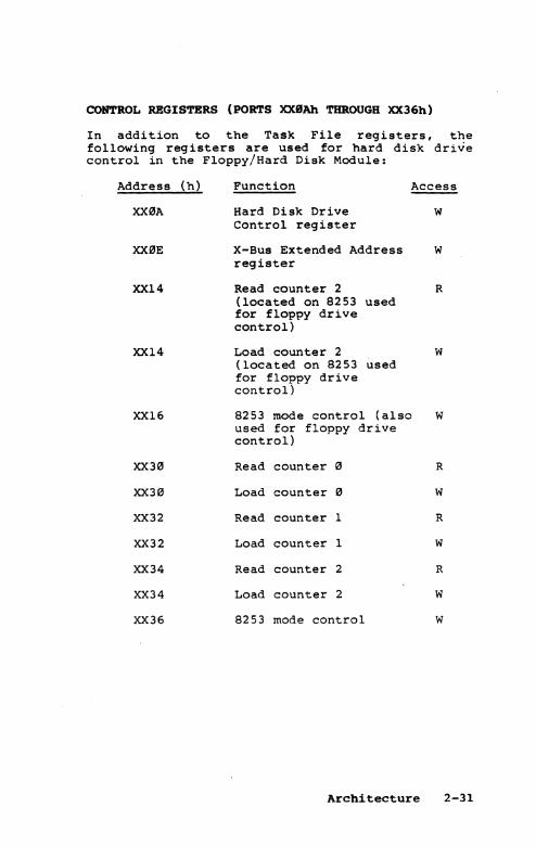
CONTROL REGISTERS (PORTS XXeAh THROUGH XX36h)
In addition to the Task File registers, the following registers are used for hard disk drive control in the Floppy/Hard Disk Module:
Address (h)
XX "A
XX"E
XX14
XX14
XX16
XX3"
XX3"
XX32
XX32
XX34
XX34
XX36
Function Access
Hard Disk Drive Control register
X-Bus Extended Address register
Read counter 2 (located on 8253 used for floppy drive control)
Load counter 2 (located on 8253 used for floppy drive control)
8253 mode control (also used for floppy drive control)
Read counter "
Load counter "
Read counter 1
Load counter 1
Read counter 2
Load counter 2
8253 mode control
Architecture
w
w
R
w
w
R
w
R
w
R
w
w
2-31
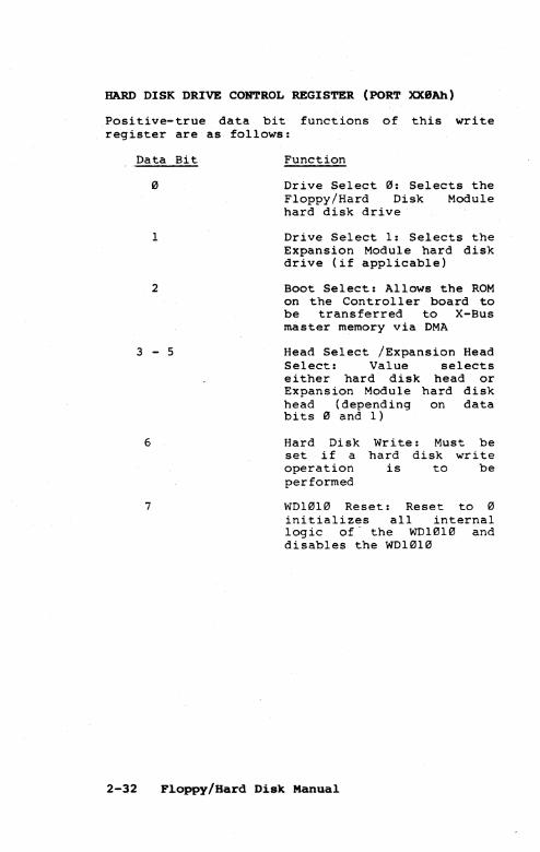
BARD DISK DRIVE CONTROL REGISTER (PORT XX8Ah)
Positive-true data bit functions of this write register are as follows:
Data Bit
1
2
3 - 5
6
Function
Drive Select B: Selects the Floppy/Hard Disk Module hard disk drive
Drive Select 1: Selects the Expansion Module hard disk drive (if applicable)
Boot Select: Allows the ROM on the Controller board to be transferred to X-Bus master memory via DMA
Head Select /Expansion Head Select: Value selects either hard disk head or Expansion Module hard disk head (depending on data bits Band 1)
Hard Disk set if a operation performed
Write: Must be hard disk write
is to be
7 WD1B1B Reset: Reset to B initializes all internal logic of" the WD1B1B and disables the WD1B1B
2-32 Floppy/Bard Disk Manual
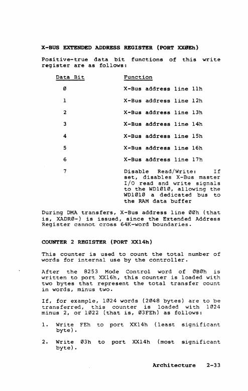
X-8US EXTENDED ADDRESS REGISTER (PORT XXSEh)
Positive-true data bit functions of this write register are as follows:
Data Bit Function
0 X-Bus address line llh
1 X-Bus address line l2h
2 X-Bus address line l3h
3 X-Bus address line l4h
4 X-Bus address line l5h
5 X-Bus address line l6h
6 X-Bus address line l7h
7 Disable Read/Write: If set, disables X-Bus master I/O read and write signals to the WD10Hl, allowing the WD10l0 a dedicated bus to the RAM data buffer
During DMA transfers, X-Bus address line 00h (that is, XADR0-) is issued, since the Extended Address Register cannot cross 64K-word boundaries.
COUNTER 2 REGISTER (PORT XX14h)
This counter is used to count the total number of words for internal use by the controller.
After the 8253 Mode Control word of 0B0h is written to port XX16h, this counter is loaded with two bytes that represent the total transfer count in words, minus two.
If, for example, 1024 words (2048 bytes) are to be transferred, this counter is loaded with 1024 minus 2, or 1022 (that is, 03FEh) as follows:
l. Write FEh to port XX14h (least significant byte) .
2. Write 03h to port XX14h (most significant byte) •
Architecture 2-33
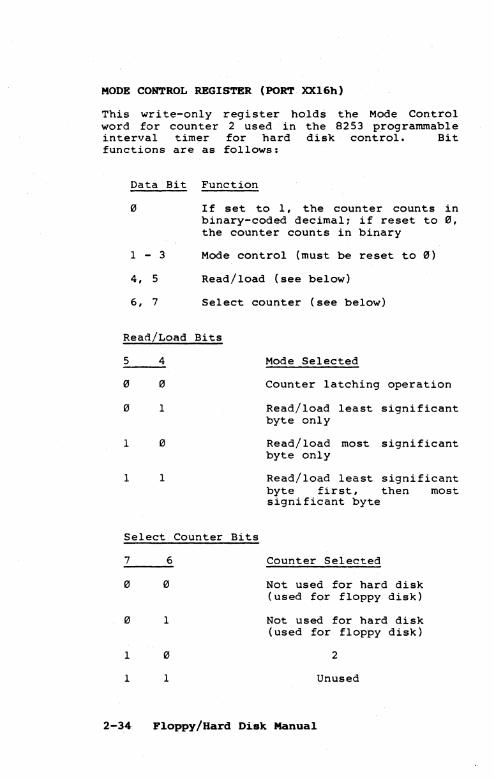
MODE CONTROL REGISTER (PORT. XX16h)
This write-only register holds the Mode Control word for counter 2 used in the 8253 programmable interval timer for hard disk control. Bit functions are as follows:
Data Bit Function
" If set to 1. the counter counts in binary-coded decimal: if reset to ". the counter counts in binary
1 - 3 Mode control (must be reset to 0)
4. 5 Read/load (see below)
6. 7 Select counter (see below)
ReadLLoad Bits
5 4 Mode Selected
" " Counter latching operation
" 1 Read/load least significant byte only
1 " Read/load most significant byte only
1 1 Read/load least significant byte first. then most significant byte
Select Counter Bits
7 6 Counter Selected
0 " Not used for hard disk (used for floppy disk)
" 1 Not used for hard disk (used for floppy disk)
1 " 2
1 1 Unused
2-34 Floppy/Bard Disk Manual
COUNTER I!I (PORT XX31iJh)
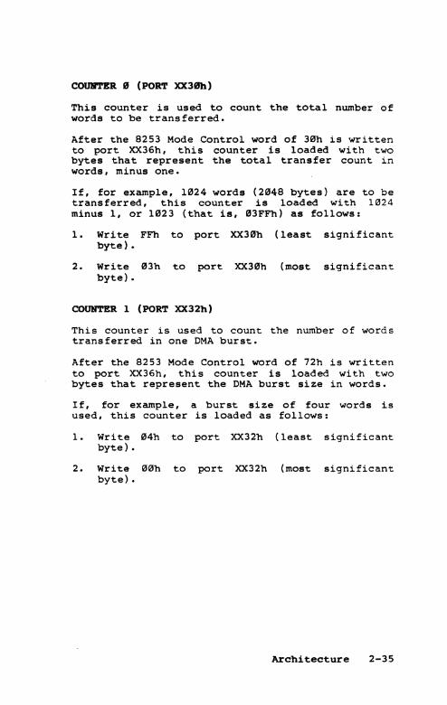
This counter is used to count the total number of words to be transferred.
After the 8253 Mode Control word of 30h is written to port XX36h, this counter is loaded with two bytes that represent the total transfer count in words, minus one.
If, for example, 1024 words (2048 bytes) are to be transferred, this counter is loaded with 1024 minus 1, or 1023 (that is, 1!13FFh) as follows:
1. Write FFh to port XX31!1h (least significant byte) •
2. Write 1!13h to port XX31!1h (most significant byte) •
COUNTER 1 (PORT XX32h)
This counter is used to count the number of words transferred in one DMA burst.
After the 8253 Mode Control word of 72h is written to port XX36h, this counter is loaded with two bytes that represent the DMA burst size in words.
If, for example, a burst size of four words is used, this counter is loaded as follows:
l. Write 04h to port XX32h (least significant byte) •
2. Write I1ll1lh to port XX32h (most significant byte) •
Architecture 2-35
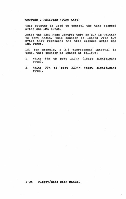
COUNTER 2 REGISTER (PORT XX34)
This counter is used to control the time elapsed after one DMA burst.
After the 8253 Mode Control word of B2h is written to port XX36h, this counter is loaded with two bytes that represent the time elapsed after one DMA burst.
If, for example, a 2.5 microsecond interval is used, this counter is loaded as follows:
l. Write 05h to port XX34h (least significant byte) .
2. Write 00h to port XX34h (most significant byte) •
2-36 Floppy/Hard Disk Manual
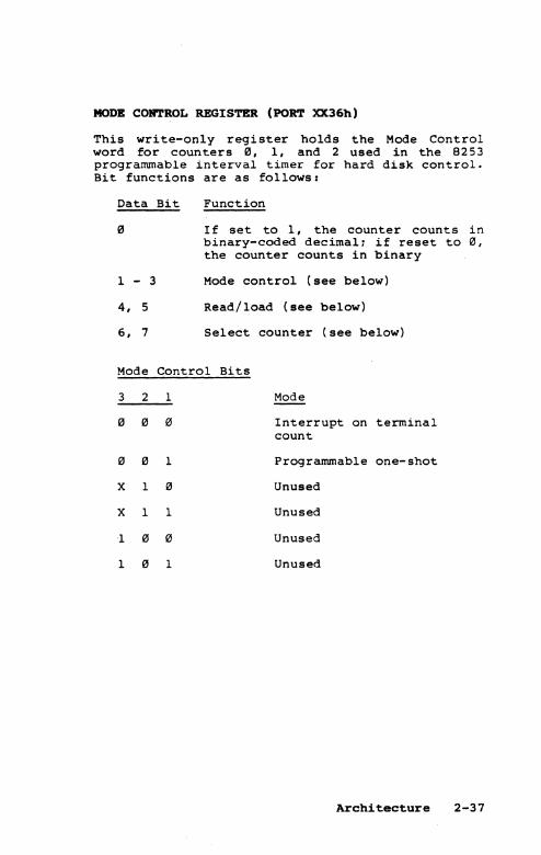
MODE CONTROL REGISTER (PORT XX36h)
This write-only register holds the Mode Control word for counters fIl, 1, and 2 used in the 9253 programmable interval timer for hard disk control. Bit functions are as follows:
Data Bit
1 - 3
4, 5
6, 7
Function
I f set to l, the counter counts in binary-coded decimal: if reset to fIl, the counter counts in binary
Mode control (see below)
Read/load (see below)
Select counter (see below)
Mode Control Bits
3 2 1 Mode
fIl fIl fIl Interrupt on terminal count
fIl fIl 1 Programmable one-shot
X 1 fIl Unused
X 1 1 Unused
1 fIl fIl Unused
1 fIl 1 Unused
Architecture 2-37
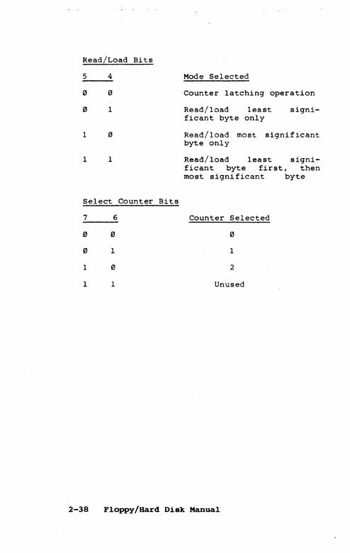
Read/Load Bits
5 4
1
1
1 1
Select Counter Bits
7
13
13
1
1
6
1
1
Mode Selected
counter latching operation
Read/load least signi-ficant byte only
Read/load most significant byte only
Read/load least significant byte first, then most significant byte
Counter Selected
1
2
Unused
2-38 Floppy/Hard Disk Manual
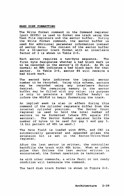
HARD DISK FORMATTING
The Write Format command in the Command register (port XX2Eh) is used to format one track using the Task File registers and the sector buffer. During the Write Format command, the sector buffer is used for additional parameter information instead of sector data. The content of the sector buffer for a 32-sector track format with an interleave factor of 2 is shown in Table 2-5.
Each sector requires a two-byte sequence. The first byte designates whether a bad block mark is to be recorded in the sector's ID field. An 0h is normal: an 80h indicates a bad block mark for that sector. In Table 2-5, sector 04 will receive a bad block mark.
The second byte indicates the logical sector number to be recorded. Using this scheme, sectors may be recorded using any interleave factor desired. The remaining memory in the sector buffer may be filled with any value: its purpose is only to generate a BRDY (Buffer Ready) to inform the WD10l0 to begin formatting the track.
An implied seek is also in effect during this command if the cylinder registers differ from the internal cylinder position. The Sector count register is used to hold the total number of sectors to be formatted (where FFh equals 255 sectors) . The Sector Number reg ister hold s the number of bytes to be used for gap 1 and gap 3. (A bit pattern of 4Eh is used.)
The data field is loaded with 0FFh, and CRC is automatically generated and appended unless the extension bit is set in the Sector/Drive/Head register.
After the last sector is written, the controller backfills the track with 4Eh bits. When an index pulse that follows the last sector written is encountered, the format operation is terminated.
As with other commands, a write fault or not ready condition will terminate the command.
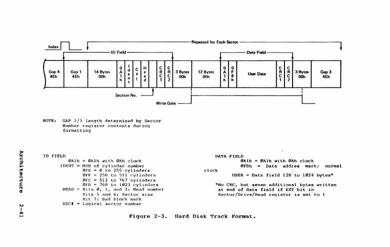
The hard disk track format is shown in Figure 2-3.
Architecture 2-39
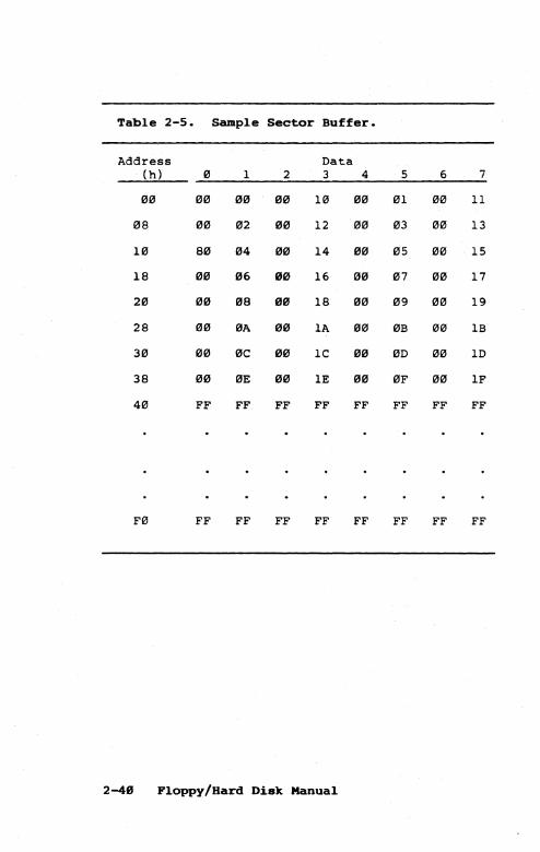
Table 2-5. Sample Sector Buffer.
Address Data (h) e 1 2 3 4 5 6 7
ee ee ee ee 1e ee .e1 ee 11
e8 ee e2 ge 12 ge e3 e0 13
1e 89 e4 99 14 99 05 00 15
18 0e e6 99 16 130 07 e0 17
20 013 98 99 18 90 09 00 19
28 00 0A 09 lA 90 13B (lUll IB
30 99 0C 09 1e 00 00 00 10
38 00 0E 00 1E 0e 0F 00 IF
40 FF FF FF FF FF FF FF FF
F0 FF FF FF FF FF FF FF FF
2-48 Floppy/Bard Disk Manual
.. rl r--------------------Repeated for Each Sector
~ L-J ID Field
I 0 I H C C Gap 4 Gap 1 14 Bytes A d C
R R 3 Bytes e y e 4Eh 4Eh OOh 1 a C C OOh
J h n I d 1 2 t
I I
Section No. ~ Write Gate ~
NOTE: GAP 1/3 length determined by Sector Number register contents during formatting
10 FIELD IlAlh = IlAlh with IlAh clock
IDENT = MSB of cylinder number OFE 0 to 255 cylinders OFF 256 to 511 cylinders OFC 512 to 767 cylinders OFD 76R to 1023 cylinders
HEAD B1tS 0, 1, and 2: Head number Bits 5 an() 6: Sector size Bit 7: Bad block mark
SEC# Logical sector numher
Data Field
I 0 0 C C
12 Bytes A F R R 3 Bytes Gap 3 User Data OOh 1 8 C C 00h 4Eh
h h 1 2
I I
L
DATA FIELD IlAlh = IlAlh with IlAh clock IlF8h Data add res mark; normal
clock USER = Data field 128 to 11124 bytes*
*No eRe, but seven additional bytes written at end of data field if EXT bit in Sector/Drive/Head register is set to 1
Figure 2-3. Bard Disk Track Format.
PROGRAMMABLE ARRAY LOGIC
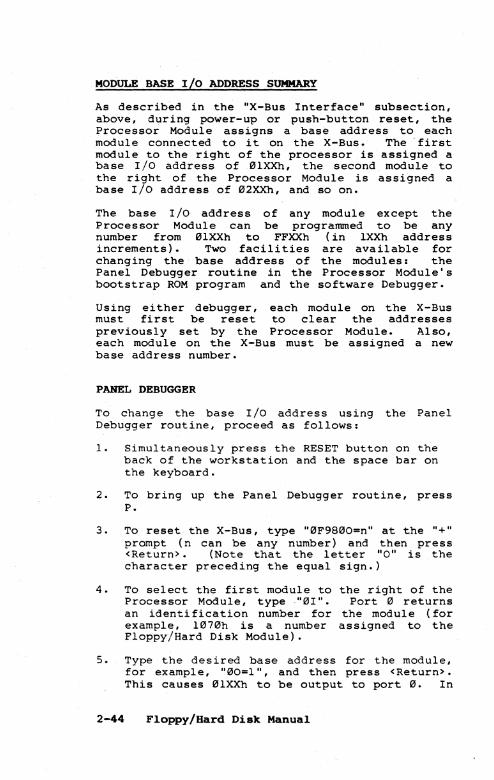
Two l6L8 programmable array logic (PAL) chips are used in the Floppy/Hard Disk Module to generate control signals. Programming examples are provided in Figures 2-4 and 2-5 for integrated circuit (IC) designations 7E and l3E, respectively. (See the schematic diagram shown in Figure 3-2, page 5, in Section 3, "Theory of Operation," for IC designation of the PALs.)
2-42 Floppy/Hard Disk Manual
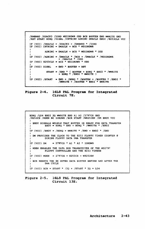
/XMEMRO /XDACK3 /IORD WDIORDWR ODD BCS BOOTEN END WWRITE GND /RST START BDRO /DISBL /CNTRINC ADRINC DMACLK END2 /8253CLK VCC
IF (VCC) /DMACLK - /XDACK3 + /XMEMRD • /IORD IF (VCC) CNTRINC - DMACLK + ses • WDIORDWR
ADRINC - DMACLK + BCS • WDIORDWR • ODD I IF (VCC) /ADRINC - /DMACLK • /BCS + /DMACLK • /WDIORDWR
+ /DMACLK • /000 IF (VCC) 8253CLK - BCS • WDIORDWR • ODD , IF (VCC) DISBL - END • BOOTEN + RST
I
START - /END • ( BOOTEN + BDRO • END2 • /WWRITE + BDRO • /END2 • WWRITE )
IF (VCC) /START - END + /BDRO • lBOOTEN + /BOOTEN • /END2 • IWWRITE + /BOOTEN • END2 • WWRITE
Pigure 2-4. 16L8 PAL Program for Integrated Circuit 7E.
BDRO ILD4 END2 20 WWRITE END Al A2 /2797CS GND 18253CS IMDEN NC IORDWR /BCR START IWB253EN 10M BRDY VCC
: BROY SIGNALS WD1B1B THAT BUFFER IS READY FOR DATA TRANSFER BROY - BDRO • END + BDRO • /WWRITE • /END2 ,
IF (VCC) IBROY - IBDRO + WWRITE • lEND + END2 • /END , .
: oM PROVIDES THE CLOCK TO THE B253 FLOPPY TIMER COUNTER B DURING FLOPPY DATA DNA TRANSFER
iF (vcc) OM - 2797CS • Al • A2 • IORDWR
, MOEN ENABLES THE DATA BUS TRANSCEIVER OF THE WD2797 FLOPPY CONTROLLER AND THE 8253 TIMERS
: IF (VCC) MOEN = 2797CS + 8253CS + W8253EN
: BCR RESETS THE 8K BYTES DATA BUFFER BEFORE AND AFTER THE DMA CYCLE
: IF (VCC) BCR - START· /20 + /START • 20 + LD4
Pigure 2-5. 16L8 PAL Program for Integrated Circuit 13E.
Architecture 2~3
MODULE BASE I/O ADDRESS SUMMARY
As described in the "X-Bus Interface" subsection, above, during power-up or push-button reset, the Processor Module assigns a base address to each module connected to it on the X-Bus. The' first module to the right of the processor is assigned a base I/O address of 01XXh, the second module to the right of the Processor Module is assigned a base I/O address of 02XXh, and so on.
The base rio address of any module except the Processor Module can be programmed to be any number from 01XXh to FFXXh (in lXXh address increments) • Two facilities are available for changing the base address of the modules: the Panel Debugger routine in the Processor Module' s bootstrap ROM program and the software Debugger.
Using either debugger, each module on the X-Bus must first be reset to clear the addresses previously set by the Processor Module. Also, each module on the X-Bus must be assigned a new base address number.
PANEL DEBUGGER
To change the base I/O address using the Panel Debugger routine, proceed as follows:
1. Simultaneously press the RESET button on the back of the workstation and the space bar on the keyboard.
2. To bring up the Panel Debugger routine, press P.
3. To reset the X-Bus, type "0F9800=n" at the "+" prompt (n can be any number) and then press <Return> . (Note that the letter "0" is the character preceding the equal sign.)
4. To select the first module to Processor Module, type "01". an identi fication number for example, l070h is a number Floppy/Hard Disk Module).
the right of the Port 0 returns
the mod ul e ( for assigned to the
5. Type the desired base address for the module, for example, "00=1", and then press <Return>. This causes 0lXXh to be output to port 0. In
2-44 Floppy/Hard Disk Manual
this example, the base address assigned to the first module is "1" or 12J1XXh. If this module is the Floppy/Hard Disk Module, the floppy drive Status register is at address 12J112JI2Jh and the floppy drive Data register is at 12J112J6h. The LED in front of the module lights to show that it is selected.
Repeat steps 4 and 5 for every module in the system, assigning a different base I/O address to each module. (For further information about the Panel Debugger routine, see the Diagnostics Manual.)
SOFTWARE DEBUGGER
To change the base I/O address using the software Debugger, proceed as follows:
1. Enter the debugger by simultaneously pressing the ACTION and A keys.
2. To reset the X-Bus, type "I2JF9812J0" at the "!" prompt, and press the right arrow key. Enter a number from 121 to 9. (Note that the letter "0" is the last character in i2JF9812J0.)
3. To select the first module to the right of the Module, type "1211" and the right
Port I2J returns an identification the module (112J712Jh is a number
the Floppy/Hard Disk Module).
Processor arrow key. number for assigned to
4. Type "1210" and press the right arrow key. Then enter the desired base address for the module, 1 to FF. For example, if "FF" is typed, FFXXh is output to port 121. In this case, the base address assigned to the first module is "FF" or FFXXh. If this module is the Floppy/Hard Disk Module, the floppy drive Status register is at address FFl2Jl2Jh and the floppy drive Data register is at FFI2J6h.
Repeat steps 3 and 4 for every module in the system, assigning a different base address to each module. (For further information about the software Debugger, see the Debugger Manual.)
Architecture 2-45
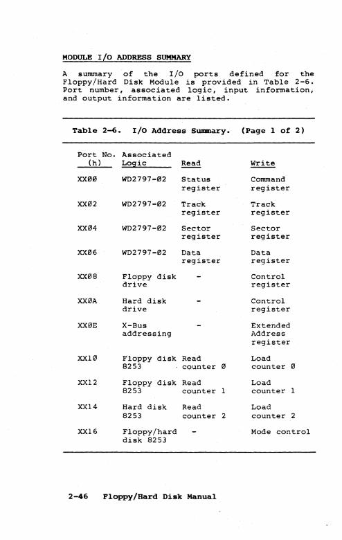
MODULE I/O ADDRESS SUMMARY
A summary of the I/O ports defined for the Floppy /Hard Disk Module is provided in Table 2-6. Port number, associated logic, input information, and output information are listed.
Table 2-6. I/O Address Summary. (Page 1 of 2)
Port No. Associated (h) LOSlic Read Write
XX00 WD2797-02 Status Command register register
XX02 WD2797-02 Track Track register register
XX04 WD2797-02 Sector Sector register register
XX06 WD2797-02 Data Data register register
XX08 Floppy disk Control drive register
XX0A Hard disk Control drive register
XX0E X-Bus Extended addressing Address
register
XX10 Floppy disk Read Load 8253 counter 0 counter 0
XX12 Floppy disk Read Load 8253 counter 1 counter 1
XX14 Hard disk Read Load 8253 counter 2 counter 2
XX16 Floppy/hard Mode control disk 8253
2-46 Floppy/Hard Disk Manual
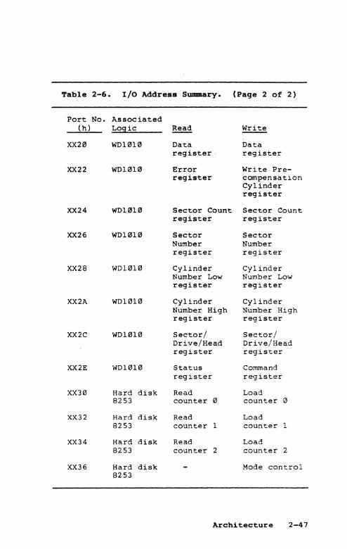
Table 2-6. I/O Address Summary. (Page 2 of 2)
Port No. Associated (h) Lo~ic Read Write
XX20 WD10l0 Data Data register· register
XX22 WD10l0 Error Write Pre-register compensation
Cylinder register
XX24 WD10l0 Sector Count Sector Count register register
XX26 WD10l0 Sector Sector Number Number register register
XX28 WD10l0 Cylinder Cylinder Number Low Number Low register register
XX2A WD10l0 Cylinder Cylinder Number High Number High register register
XX2C WD10l0 Sector/ Sector/ Drive/Head Drive/Head register register
XX2E WD10l0 Status Command reg ister reg ister
XX30 Hard disk Read Load 8253 counter 0 counter 0
XX32 Hard disk Read Load 8253 counter 1 counter 1
XX34 Hard disk Read Load 8253 counter 2 counter 2
XX36 Hard disk Mode control 8253
Architecture 2-47

3 THEORY OF OPERATION
INTRODUCTION
This section, which provides detailed componentlevel descriptions of the hardware incorporated in the Floppy/Hard Disk Module, is directed to the engineer who needs to understand the Floppy/Hard Disk Module at the component level. Each functional block shown throughout this section is described in relation to the logic that performs the function. In addition, schematic drawings are provided in Figure 3-1 to supplement the text.
Theory of Operation 3-1
CIRCUIT DESCRIPTIONS
Detailed component-level circuit descriptions are given for the foilowing:
o X-Bus module identification
o local module data bus interface
o transfer acknowledge generation
o Floppy/Hard Disk Module device decoding
o floppy disk drive controller logic
o hard disk drive controller logic
o disable read/write
o hard disk drive boot ROM
o hard disk drive controller RAM data buffer
o RAM chip selection and addressing
o RAM data direction
o direct memory access transfers
o state sequencer
o hard disk drive read/write circuitry
o 8253 programmable interval timers
o power supplies
3-2 Floppy/Bard Disk Manual
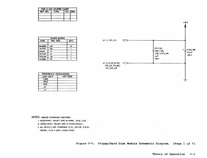
PWR • GND LOCAT1!/\ CMART REf. DES l'{PE. +S'I GIIIO
SPARE GoATES l'{PE REF. DES. QW.
7-4L&_ 10f' ~
?!4L~"'" 96 I
"'~7'" IF I
?4L!.f2.S Ie. I
7"51~'" I~ I
74 56" .ooA I
REFEReN('E DESIGNATION LAST USED NOT USED
C40 RP4 Alq
"" LI
NOTES: UNlESS OTHERWI&E speCIFIED.
1. ReSISTANfE VALUES ARE IN OHMS, 1/4>1, ± 5% .
2. CAPACITANCE \IlI.LUES ARE IN MICROFARADS.
3. ALL DEVICES ARE STANDARD '.'4 ,'fila 20,12" 24,
14' 28 ; PWR • GNO (ONNEC.110NS .
Figure 3-1.
JI-I,2,ln,120
"I- 5,15 ,25,35,45, 55,,"5,75,85, Q5,105,II5
C4-C21, C2'S-C33, C35-C37,C)q .I .... F 50V
Floppy/Hard Disk Module Schematic Diagram.
+5V
+ C34,C3& 47 ... F
25V
(Page 1 of 7)
Theory of Operation 3-3
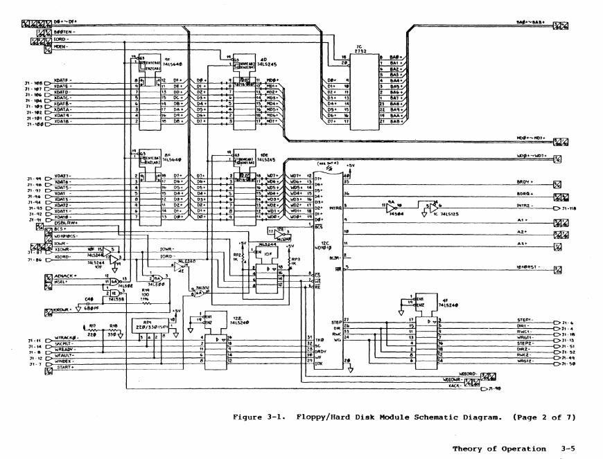
~, OCI·-Of·
1'2 8.fTEN- " m IOIU> -~
MIlEN-
~ Elltcu 1:'~.' fill'"
:n - '.11 llOAlF - 8 12 DF+
11-'" XOA't - q I""--'-~ " DE. +
l.·tee. 'DATD- 1~ f3"DD.1 l<OA1G- 51---1.-.,.. ;:;. '5 Ot.+
1.- .. , 'O"TII- .1---~ 1'-"2
l<O"TA- 3r----- r,~ ~::/ )(QAlq- 4r-< 3'-'.' 2~ I'" 08+/ 7'-'1"_ XOA1&-
'---
~" E"nUl74L~ Nt.,..}
J'- qq )(DA.11- 2 t8 07+ lQ)AT. - 3 "'-'----'" H 0 ...
3'1-Qe 'JtOA1S- 4-~ .,,-<tJ llOAl - :;- '5 ii'i+ 1i-ct. _15- 8-~
Jt-q4 l<OATZ- q-I"~I
~~~:: ~ .-)COAl'- 14 01-X""".- 1- I'~ o,·~ J'-:" OSBLRW+ -
~. 8es ..
~ wo",'t)tS-
1"71!2 9 IOWR-
J'f-"ff' xIOWII- .,. '''1'.5 IOWR-
XlORO- 14I.~M4I-("" 3 I 10RD-;"'-8"
14l~4.1" ~~~O RZlA[NACK+
1 .olE
~~r.A'!l 29.' I!=iI ,,"'l- ~t 14LS." 12!11 .. 3 It'" 2 t. 100
CA' 14L558 , ...
~8'PI' Ir-'I_-~ ""'" RPt .41
, RI1 Rte ZUI/HC2I'StP) I
2Z, I 33"~ "~KGI- 5 4 2 ~
,t-fi ;11 ~ t .. _''IT - I
1t- e D ::!~_-1t -12. wINge_· :7t-., ;;:;. START. --
I?A!I
"
~," lk : 14LSZ45 28'
Of· q " ~. ~ 01- 8~~ 02+ 7-~ ~ 03' :===~ ~ 04- ~ os- .. -~ ~ 0.· 2-~ ~ Dl- 3-~ ~
-
~-• c=...a., 14lSZ45 "., (_II SRT") +&'1
-~ ~ 01· 2: ,. \D7+ ~01+ -~ 0"- 3~tl)1106 ..
os- 41---~+ ~06. J!J
04- 51---~. .~:: * 03' .t---~
::: :~ DS· Oz- ll---~. MAli' 01- 81--- ~,-< ...;0.;,,. DZ·
DG'> qt---~ ~ 01> of> q
'- 'ezs ~ " .
v~. _sv 12(, ..
wD1I1i', RPl .. IOF
~ '" .. RP3 8C3<-'K
~~~ RI{~ L...- a l:!.
1---<4 '-WI. 1---'2
~ Re
'-----
1 14 tZ£.
!T!P 21 Nl 74LSZ4ft 0", t"
AWe 33
4 ~ v • " TK' we,. 24
2~18 32.c. ,,~q Z8 DROV
'1---'. !. wF 8~'Z lq lOX
~ '-
1G UU
SAf+
l' IA' +1 I. BA2+1 I: :::1 3 ~. 2 ... ,,+
~ , BAa • ~ I.q IIM+I 121 IA8·1
If qA .. 5 " 14~ tc. 14t.S1Z5
• Nt • q ...
ENf l4L5Z4f
11 ~ ... '5-&
I 11-q I 13-
~ I 4-'" 2-18 8-Z 6-4
- warQQD- tr>tnI
'oIDlDW"~: ''''K- ;n-...
..,."'V" ••
MDClf+-M01.
WO' ....... W01.
8RD'f -
&DRQ.
INl1\t-
AI.
"2-"5'
tf)1ftRST -
STEPof-
OIJU-RWC..-Wt«.H-STEPZ-DlRt-RW(.2,-
WRQlt-
~ """'-""
~ .-au
IT7I ~
~ ..",
,..,...." ....... 11-
-I\2r2I -= I£I!Ia!I
-172.1 """
.../J2I ~
It-D71-
7'-1'< :rt-}.-;n-
~ ;n-
"II
• 4 18
Figure 3-1. Floppy/Hard Disk Module Schematic Diagram. (Page 2 of 7)
Theory of Operation 3-5
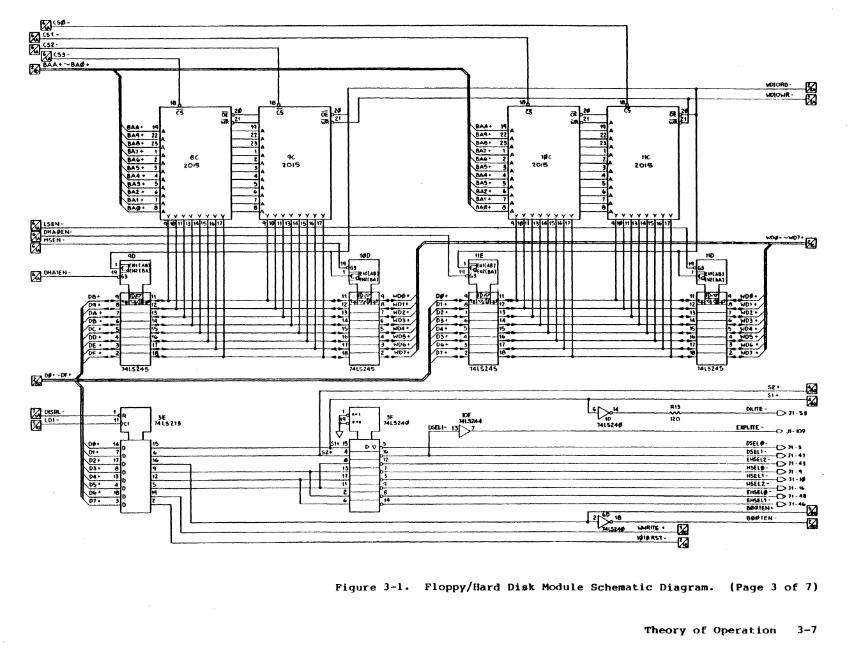
r.=:: (52-
~f6l.I(~'-I'T7I BAA ........ 8A_.
I'!?I OOSL-
~LDI-
18 IS (5
~A BAS. n
~-I 18r--~ 74lS 45 ~
, R
'U [I 'E 14lS21!J
, ... . q ... .
WDlORD- IV!
~":""J, ~ •• 'IO, tq . 3 MltlAl t NtIAa) lUlU)
0If- q tt ff " HOf.
52-51+
~ 1'~~~~L-________ ~RN"~ __________ ~"'~n~'~-~C>]1 ~,~ L.SlA" ~IO 12:0
~I J4 _ 14lftZ4' [ .... "E-I - V)-~f--------------------------------------------------~~~--C>JI-~
~ 0 1-'~::..S-------------------------------+S:-:Z~+" .. -,t5:;-J4 ~ ~ :~~~.- D ~ -,
~~ ~. .----1.==-----1P;-~':=-==================================-~-~~".~:g::::~ ~: 12 'l~- 3" HSEl~]t_" :~ 0 ! '; _ : ",SHl.- DJ'- t. ~~lll ,,~ ,. =~:~1'-4'
------ L-______________________________ -----_____________________________________________ ~12,~)~'8~--------~==----------~::~:~~~E:~;~-C>---'-·--·.~.~~ _ ~..sz.. .... R~ - 1'21 IdItlI
L-________________________________________________________________________________________ ~I.~I~'~RS~l~-~~
Figure 3-1. Floppy/Hard Disk Module Schematic Diagram. (Page 3 of 7)
Tbeory of Operation 3-7
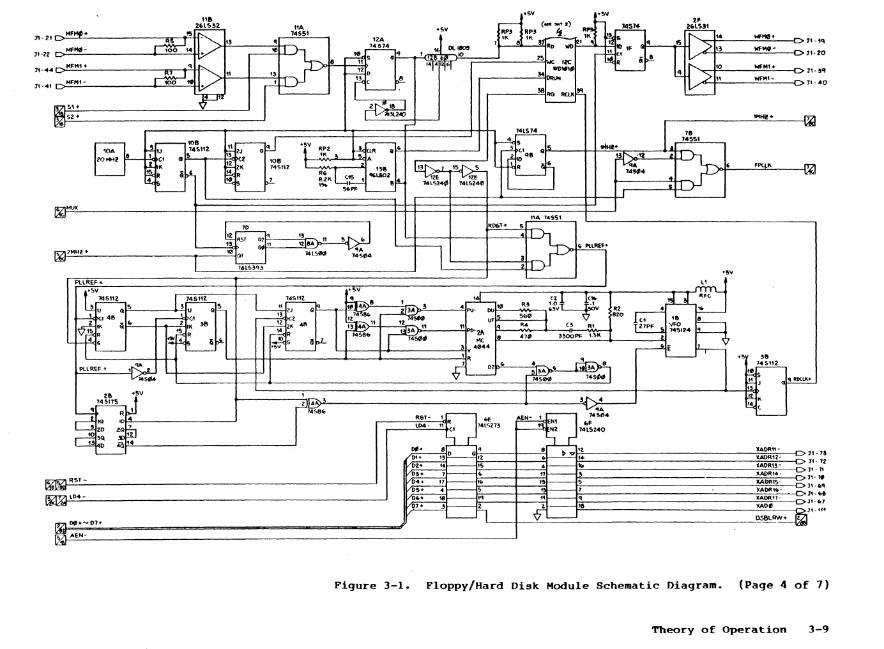
~ 11A +SV 1~"'5V (.n.,. 2)
J\-2\ D.::MO-"",,=+:-.-______ -;;r-,"''''tu;:::-- 74S5\ '2A ~ RP. RP' ~ __ 'l.'L-.1n 11- '-...,>-f,~.---__;;:~h_-., 1 1K e tK !" RO "wo
J1-22 MFf1tli- 1;00·'4 .. ~k> ,. ~ q 1 ,16 D1.1~ I I V 8 r--i1 s t\I'f--r--'-<;l~'~i.~)'IO"-;:::=:::::!.---~25?J...,~
HFM, .. ~ I to ~~+--';t. ·if4FR .... J1- ... 4D,!:!C"'-'-'--------~..",r-",",,11lP- 11 13, t--i?' D 340:;"'" J1-41 MFHt- 1.00 '.U .. / P ~~ Lri I ,...-___ ......:.38!!j"", fl<l.Kj!!
~I"V.~S~\~.'_ ____________ ~~ ___ ~ ~~ L......-...-
~S2+ ~ 'MHl'"
11.6. 14SS1
RD&T.f- 5
~PL:.:L"'R~;:;F-.--...,~~ ~
Z& J'SV ~
23~ R 1
to 'D~["!..--------------J " ZO o!QJ!=,
,.-J!! 'Q ~~ ~~r'4~-------------...-J XADRl1-
" 15 XAORl1-
XAOR'3-,t· 12
Jl.ADR,'4-Jf -11
XADR1S-C>11-'"
)(AOR1Cio-11·fiI" J'-~8
!CA[)R'1-Jt. '" "'De "_ u",
RST-
l04-
__ ~L~"
AE.N-
Figure 3-1. Floppy/Hard Disk Module Schematic Diagram. (Page 4 of 7)
Theory of Operation 3-9
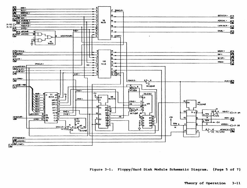
121 CIllO-
(>ITo. INtO. -~ DoS8L- ::;
172I11'11C5 - BIt""-1114+
Bes,,- It!
~--~~------------------------------------------~~~---4~
ACW-ID\
~ 0 sc AI'" '!IV '5V I L ~ ~ IIt53A'~ Z""Z+ ! ~R 14~~' l!lO
"'s- 5 =~ ?- ,---+_ .. 2;:"~"=-Z,;..'_-;2H> ~ GATll ,'~ '5 t--t::2<11~-_-;: .. 1~Cl" "II t'~... <Ntt!;'3;----+t---_t-t--",D4 4Q' [ ~ • ""'I all'; ~'" .-----;'3 ~ OUT ,," END + I 7.- ~ .. " ~IZ 11 "&HE'
wers,.,,- ZI a Cll t& ..... 2. !Z 03 ~'~"~=2dr--' loflS,' C \2 _ 2 0.'" .... ;:;. (0110- :::: ~; ~~ ~~... ~ D2 ~ ~.8 1 a QC =r 'f5' ~ ~ L4 ,,:. 1 AEN-~
'-----' ... IK ~_DI ~~: 1511~l'4 "FlO S "-9 I II< .~v 'DRas- n-58 '-i ________ 1lH=""'(l;;K"'.~q II 00 .... ----= IK ~
14tS'lS.. 14L5.'" 17 - J a 12 _OCt 1271 L-______________ --' L-t __________________ ++--'Ir---R-1 <or T4L5...a 1t!!'!I
r-~t----_t~~~tN 4e 14lS2411
1t-8'I
Figure 3-1. Floppy/Hard Disk Module Schematic Diagram. (Page 5 of 7)
Theory of Operation 3-11
1,-57
"-58 J't-18
D 011 -I7ft-
D13-
If7L\)jl'-OF'
""'" ~DMAfN-
11-""
"-<4 ], -~1
.1t-.!" 11-~!
:J,-" .. .1t-"' 31-'. 1'-11
~PI'N'" ·,v l RP21
....... lIADRF- '" XADR.E-~ADRO-
xAORe.· AADRB-)(ADRA-l<AI)Rq-
XAOR8-
IDIIDWR-
""" Ii.2\.toRO-
"""
~-88 XRST-
~"SEL-
l'f:!tllORG+
.D 13 7
.~ Z5lSts21
r=1J. bf) 11 ~ 1 N1 • RS1+ ,: R15D ' , .SV
~i 14Lt:"." ,q N2 SF Iq 5E 1et W18e RP2 tK
RI I-~rt=-- i
~ '" .~v I I tq EN1 qe • ~ ... 14 2 3 : ~---= ~ ~:: -~ z ~ ~ I I
4-5 p'1~~ I Nl nr----. 1"4 L_ '5 5 .--7 5-~ 4 r---- 1b 05+ lP3 it) &- I'-_~-J
"-7 8-q ~~~ ~r--~ .r' Ole- I, "'V De·
.. f------ , .. 11-12 .r--~ 011- fS~~ OCt· 2,-18 "--'. ,.;-~ ~r----~ 012- 13f-----~ 1Ic--IZ 15 - ". 15c--~ 8r--12 0'. P13- " t--- ~ DB' 11 f----- q 11--,8 12~~ ~r--~ .. g f----- • DC<
f----- .. 00 • '---- - - '7 '--- r---- •• DE<
f----- 'II OF'
'--EN'. ..P2I
1 xPOOT. """ J'·1t7
.. ~v 7A
.~ ;l4LS74 .D ~ 4 =-'-'- ~5 4 ~" 5
I Q~f- HSEL· 5 ~ID "I"--Z Q 4 14L5Z.' '5~ ~><,'2" _ •
I~ ~'."Z" ;~5 Q~ 60
.sv _
l'IU\2<O ~. RST- r.?I 11 • 34A L I.M ... 14~t
~ [Hf-
~ 1% e ~ 13 ~A.
8 q 74LS2f&
.0 I~ MSEl+ IF?I 1At..sZAO
"""
Figure 3-1. Floppy/Hard Disk Module Schematic Diagram. (Page 6 of 7)
Theory of Operation 3-13
JI-80
JI-7q
TR"CK. -
WRPROT-
~ tHOU-
~ ~fAll'f-
IT7lMO'+- MI77+ "-""
~ OM+ """'Vl' ..... 1+ fi!7I\C!I EwOI+ 1M" r!2I-BZ!!CS-
""" If7I [OWA-
!dill P7\.lORO-
1f7I""" "2' ~~A" 5 & 8253 (lK.-v1!o
® INt +
IT7I O!I' -D7 ~
~ "SEL-
""'" m EN.-1DI1<3I8001TEN -vm.J
)Co\OM-
)(AORS -
~I-.' ~1-8~
JI·e2
XAOR1-MORZ-.JIADR, -
~ 2 A'· ,
RP' I 1291/3'0
l' III I' q
I I
1.1'-,. •
•• 14Slt4
~
-~ 81~3 "6f D' '
MD7+
1" 112 "". ""'0-~ C" 0,3 MOS'
04 4 M04-n(.1 03 :
HD!-+
Z. ~ MPZ + D2 7 MOl"
21 -0' HOG!-".8 zt WR
Zf RD
04~1 1~ :~ G'1.4 5 " 18 <..Z 01 "3 -4 if »=-
74L'H8 ~
flF
~ , 4 q ~
~ , I>ii-
~ '5 2 14
3 • ~ - R:.R:CS-
~'14
~v ~; 15~ 5- 1'A\..S240
~ 74L5Z40
• ,~
eN
2G 27"11
341'16(. " 2 1>0 ,e
'"- w;" .51-- S
S' TJ ST. IS 4- ... 32 .... '" IlIAC , ... 17- ,
en zo ~ ~ -1 .~o
41PF II ];'~ ...!. - '2 GN() ,. .. Iu ~ 11 Tt'i
37 TP~~ -.....
t4 D7 n u
"" t.lK U '2 1>5 .~.
11 04 RB
'" O. ",UK q
RPW '. 02 8 D. EHI'
~ Rq ~ IUtK 7 1lI43
t8 OG! tS
, .'. ~ WtO HLT ~4 ".2 3O.1t1;:
"""" ~ WPW JozrtR ." q.3tK tn '7 ~t
z.t 410PF
; ~ " n
OIl •• It
" .... ,. !'!'! • IS iE • AI
INTRQ
I _'V
~'8 5 AOI All q 'K
1.E 8
141:5'81
Q I 13 '0 ,
q lE '4t52#
Z 18
J 4E
~--40 Q2 14LSl4'
~ 40 a' ~r-; 1 e:7 0 Q ~J!D Q~'-~~O QJ--
i~ ~ '---
7P' ~ ..
ttf'.,q V14t~Z" V6D 14L'2401
~ 4 f~ 5 'Pii-.,V~ ... '!>it
'~LN-• ~ 2
A" 3 ,~ , ,
J'V RP4 J ,1\
4t--, "- 0'. 4£ flO
14L524.
R'~
120
: '" 4
~t"z
to ... - Il/I
"""0
wAttATA -
\ltlW&ATE-
STEP -
OIR -
OS"-
>tC7T~-
RI)QI,1'A·
FA:LK
OOliTE -
""" KDRGl4 -
XIHT1I\S-
~
~
,....
1. -,.,
l' - Zq
1\-21
l' -,8 ,. -lJ , .- 24
-f.21. ~
l' -34-
1'-54
lUI
""" 1'-~
MOMHl.IlE- ~ 14 -t;Gt
srDE5£L-
U~"cs- JiZI ~
WOI ...... - Il7I
"e'53"'- ~ U!I
lO'! - ~
~
Figure 3-1. Floppy/Hard Disk Module Schematic Diagram. (Page 1 of 1)
Theory of Operation 3-15
X-BUS MODULE IDENTIFICATION
The Processor Module communicates with the Floppy/Hard Disk Module through the X-Bus interface as shown in Figure 3-1, page 6. Base addresses for the various I/O ports and registers are assigned by the Processor Module when a powerup reset or a manual (push-button) reset occurs on the X-Bus as XRST- (X-Bus Reset), or when XPIN+ (X-Bus Priority In) is reset low, signifying that activity on the X-Bus for the Floppy/Hard Disk Module has been suspended.
XRST-, connecting from Jl, pin 88, is inverted at 60 (pin 3) and driven to NOR gate 6A (pin 3). A low XPIN+ connecting from Jl, pin 116, is inverted at 7F (pin 3) before connecting at NOR gate 6A (pin 2). In either case (that is, a reset or low X-Bus Priority In), a high signal at pin 3 or 2 forces a low signal at pin 1 of 6A, to clear D flip-flop 7A at pin 1 and clear I/O Address register 5D at pin 1.
When 7A is re·set, a high signal is generated from pin 6 as the complement of ENl- (Enable). In addition, XPOUT+ (X-Bus Priority Out) is forced low at pin 5 of 7A, which causes all X-Bus activity for modules farther down the X-Bus (that is, to the right of the Floppy/Hard Disk Module) to be suspended via connector Jl, pin 117.
XPIN+ then becomes high to signify that the Processor Module wishes to identify the Floppy/Hard Disk Module (that is, assign the module a base I/O address).
The Processor Module reads I/O address 00 from XADR8- through XADRF- (X-Bus Address Lines 8 through Fh) via connector Jl, pins 60 through 64, 66, 76, and 77. The high eight address bits (XADR8- through XADRF-), which represent port 00, are buffered and inverted at 5F to the A-side inputs of comparator 5E. (Note that XPIN+ is inverted at 7F, pin 3, enabling 5F.) Since I/O Address register 5D was previously cleared at pin 1, the B-side inputs of comparator 5E also connect to eight low bits, and therefore compare as equal wi th the A-side inputs, signaling MSEL- (Module Select) from pin 19 of 5E.
During XIORD- (X-Bus I/O Read), shown in Figure 3-1, page 2, IORD- (I/O Read) is generated at buffer
Theory of Operation 3-17
10F (pin 3) via pin 86 of connector Jl. As shown in Figure 3-1, page 6, IORD- is inverted at 6D (pin 14) and NANDed at gate SA (pin 13) with the high signal from pin 6 of 7A, and with XPIN+ and MSEL+ (pins 10, 12, and 9, respectively). A low signal is, therefore, generated from SA (pin 8), to enable buffers 8E and 9E (pins 1 and 19).
Note that any time the Floppy/Hard Disk Module is selected (signified by MSEL+, as shown in Figure 3-1, page 2) and either XIORD- or XIOWR- is pulsed (via connector Jl, pin 86 or 87), XACK- is generated via connector Jl, pin 90. XIORD- or XIOWR- is buffered at l0F (pin 17 or IS, respectively), generating IORD- or IOWR- at pin 3 or S, respectively. Either IORD- or IOWR- forces NAND gate 8A to generate a high signal (pin 3), which is NANDed at gate IE with MSEL+ at pins 2 and 1, respectively. This forces XACK- at pin 3, which is generated back to the Processor Module.
In summary, when a power-up or manual reset occurs, or when activity on the X-Bus for the Floppy/Hard Disk Module has been suspended, and the Processor Module issues an IORD- command to port 00, signified by four high signals at the input of NAND gate SA (pins 10, 12, 13, and 9) shown in Figure 3-1, page 6, a low signal is generated (pin 8), enabling hard-wired buffers 8E and 9E, signifying that an I/O read of port 00 has occurred, c.ausing the Floppy/Hard Disk Module to output its assigned identifier number.
Since BE and 9E are hard-wired, low-order data lines D0+ through D7+ (Local Data Lines 0 thorugh 7) are assigned identifying bits (that is, an identifying code) of 70h, and high-order data lines D8+ through DF+ are assigned identifying bits of l0h. Therefore, l070h represent!S the Floppy/Hard Disk Module.
Note that input signals at pins 11, 13, IS, and 17 of 9E are pulled high by I-kilohm resistors at RP2. Future expansions connecting to DT0- through DT3- (Drive Type 0 Through 3), however, will vary the identifying code between l0h and lFh. Therefore, .future identifying codes may range from l070h through lF70h.
Local module data lines D0+ through DF+ are interfaced to XDAT0- through XDATF- (X-Bus Data Lines 0 through F) via data transceivers 8F and 9F
3-18 Floppy/Bard Disk Manual
(shown in Figure 3-1, page 2), which are enabled at pin 19 when MSEL+ forces a low signal at NOR gate 6A (pin 13). Since XIORD- is active at 8F and 9F (pin 1), data is directed from D0+ through DF+ to XDAT0- through XDATF-.
In summary, during the I/O read of port 03, the Floppy/Hard Disk Module identifier, l070h, is generated to the Processor Module via the X-Bus data lines.
Once the Processor Module receives ~he l373h Floppy/Hard Disk Module identifier, it writes the base I/O address for the module into I/O Address register 5D (shown in Figure 3-1, page 6). This I/O address defines the range of I/O ports reserved for the Floppy/Hard Disk Module. The Processor Module issues an I/O address via loworder data lines D3+ through D7+, and that becomes the high-order eight bits of the 256 I/O address range, for example, 0lXXh or 02XXh, depending upon the physical location of the Floppy/Hard Disk Module. During the identification polling sequence, the module adjacent to the Processor Module uses I/O ports 3l00h through 01FFh, the next module uses 3233h through 02FFh, and so on. The module identifier is stored in a memory table for use by the system. (See Section 2, "Architecture.")
When the Processor Module writes the base I/O address to the Floppy/Hard Disk Module, IOWR- is inverted at 6D (pin 5) and driven to NAND gate SA (pin 4). A low signal is generated from SA (pin 6), clocking I/O Address register SD (pin 11), which is loaded with the base I/O address sent by the Processor Module.
Note that the following conditions are input at 5A during an I/O write to load 5D:
o MSEL+ (pin 5)
o High signal (pin 1) generating from 7A (pin 6) as a result of the reset or suspended activity of the Floppy/Hard Disk Module
o High signal at pin 2, generating from pin 5 of D flip-flop l2A. During the IORD- cycle, l2A is clocked at pin 3 to generate a high signal at pin 5 (resulting from XPIN+ at pin 2), This high signal connects at 5A (pin 2).
Theory of Operation 3-19
Since the inputs at 5D. consist of the module base I/O address, the outputs of 5D do not compare with the outputs of SF at comparator 5E. Therefore, a high signal is generated from 5E (pin 19). Simultaneously, D flip-flop 7A is clocked (pin 3), and a low signal is generated at pin 6. This low signal forces NAND gate SA high at pin 8, disabling module identifier buffers 8E and 9E (pins 1 and 19).
In addition, just as with XIORD-, XACK- is pulsed from pin 3 of NAND gate lE (shown in Figure 3-1, page 2).
As shown in Figure 3-1, page 6, once flip-flop 7A is set and XPOUT+ is generated from pin 5, the low signal at pin 6 of 7A disables the gates at SA at pins 10 and 1, and only the address written into I/O Address register 5D causes the module to respond to an I/O read or write operation from the X-Bus master. A high signal is generated from pin 5 of 7A as EN1+. As shown in Figure 3-1, page 7, ENl+ is inverted at gate ID (pin 7) and driven as MODENLITE- (Module Enable Light) via connector Jl, pin 56, indicating that the module has been identified.
To summarize, input/output reads or writes to addressable devices within the Floppy/Hard Disk Module, such as the WD2797-02, WD1010, or one of the 8253 programmable interval timers, are performed when the Processor Module places a base address for the Floppy/Hard Disk Module (such as 01XX, 02XX, and so on) on the XADR8- through XADRF- lines and the address for the register within the device (such as XX01, XX02, and so on) on the XADR1- through XADR5- address lines. Next, data is placed on the XDAT0- through XDAT7- data lines while either XIORD- or XIOWR- is asserted.
Note in Figure 3-1, page 6, that XDMAEN- (X-Bus Direct Memory Access Enable), which indicates that a DMA cycle is in progress, causes comparator 5E to become disabled at pin 1. During a DMA cycle, the XADR8- through XADRF- lines may contain memory address data not to be mistaken for a module base I/O address.
3-28 Floppy/Bard Disk Manual
LOCAL MODULE DATA BUS INTERFACE
X-BUS DATA INTERFACE
Transceivers 8F and 9F (shown in Figure 3-1, page 2) are used as the interface between local module data lines D0+ through DF+ and X-Bus data lines XDAT0- through XDATF- (from connector Jl, pins 91 through 94, 96 through 104, and 106 through 108). The low-order data byte is connected to 8F, and the high-order data byte is connected to 9F.
Both transceivers enable when either ACK+ (Acknowledge) or MSEL+ are active at NOR gate 6A (pin 12 or 11, respectively). ACK+, which signifies an I/O read or I/O write, is generated when the X-Bus master issues XDACK3- (X-Bus DMA Acknowledge, Priority 3) via connector Jl, pin 57 (as shown in Figure 3-1, page 5). XDACK3- is inverted at 7F (pin 9) and driven as ACK+. MSEL+, which signifies that the Floppy/Hard Disk Module has been selected, is generated when pin 19 of comparator 5E (shown in Figure 3-1, page 6) becomes active-low. This low signal is inverted at 6D (pin 12) as MSEL+. (See the "X-Bus Module Identification" subsection, above.)
In summary, when either ACK+ or MSEL+ (shown in Figure 3-1, page 2) is active at NOR gate 6A, a low signal is generated from pin 13, enabl.ing 8F and 9F at pin 19.
During an X-Bus master I/O read cycle, XIORD- (via connector J 1, pin 86) directs local module data lines D0+ through DF+ to X-Bus data lines XDAT0-through XDATF-. During an X-Bus master I/O write cycle, XIORD- becomes inactive, and data is directed from XDAT0- through XDATF- to D0+ through DF+.
FLOPPY DISK CONTROLLER DATA INTERFACE
Transceiver 4D (shown in Figure 3-1, page 2) is used as the interface between local module data lines D0+ through D7+ and local floppy disk data lines MD0+ through MD7+ (Floppy Data Lines 0 through 7). Transceiver 4D is enabled at pin 19 when Programmable Array Logic (PAL) chip 13E (Figure 3-1, page 5) issues MDEN- (Floppy Data Enable) from pin 12.
Theory of Operation 3-21
MDEN- is active when any of the following conditions are met at 13E:
o 2797CS- is active at pin 9
o 8253CS- is active at pin 11
o W8253EN- is active at pin 17
2797CS-, 8253CS-, and W8253EN- are generated from 1-of-8 decoder IlF as described in the "Floppy/Hard Disk Module Device Decoding" subsection, below.
During an I/O read cycle, IORD-, which connects at pin 1 of 4D, directs local floppy disk data lines MD0+ through MD7+ to local module data lines D0+ through D7+. During an I/O write cycle, IORDbecomes inactive, and data. is directed from D0+ through D7+ to MD0+ through MD7+.
HARD DISK CONTROLLER DATA INTERFACE
Transceiver 10E (shown in Figure 3-1, page 2) is used as the interface between local module data lines D0+ through D7+ and local hard disk data lines WD0+ through WD7+ (Winchester Data Lines 0 through 7). Transceiver l0E is enabled at pin 19 when WD1010CS- is generated from 1-of-8 decoder IlF at pin 12 or 13 (see Figure 3-1, page 7, and the "Floppy/Hard Disk Module Device Decoding" subsection), and when either of the following occurs:
o START+ is active at PAL 7E (pin 12), shown in Figure 3-1, page 5, which indicates that a DMA cycle is in progress.
o DSBLRW+ (Disable Read/Write) is not asserted from the X-Bus master via X-Bus Extended Address register 6E (pin 2) shown in Figure 3-1, page 4. (See the "Hard Disk Drive Controller Logic" subsection, below.)
As shown in Figure 3-1, page 2, either of these conditions causes NOR gate 6A to generate a low signal from pin 10, enabling the tristate buffer 10F at pin 1. When enabled, WD10l0CS- (which was issued to enable the \-101010) is generated from pin 16, which loops back to pin 2 and, consequently, is driven from pin 18 to l0E (pin 19).
3-22 Floppy/Hard Disk Manual
During an I/O read cycle, IORD-, which connects at pin 1 of l0E, directs local hard disk data lines WD0+ through WD7+ to local module data lines D0+ through D7+. During an I/O write cycle, IORDbecomes inactive. and data is directed from DO+ through D7+ to WD0+ through WD7+.
Theory of Operation 3-23
TRANSFER ACKNOWLEDGE GENERATION
During an I/O read or I/O write cycle, IORD- or IOWR- forces NAND gate 8A (pin 3) high as IORDWR+ (I/O Read or Write) as shown in Figure 3-1, page 2. IORDWR+ is NANDed with MSEL+ (signifying that the Floppy/Hard Disk Module has been selected) at gate lE (pin 2 and 1, respectively) to generate XACK- (Transfer Acknowledge) back to the X-Bus master via connector Jl, pin 90.
FLOPPY/HARD DISK MODULE DEVICE DECODING
As shown in Figure 3-1, page 7, 1-of-8 decoder llF decodes X-Bus address lines XADR3- through XADR5-to generate appropriate read/write commands. Decoder llF is enabled at pins 4, 5, and 6 when the following conditions are met:
o The Floppy/Hard Disk Module has been selected, signified by MSEL- at pin 4.
o Neither a power-up reset nor a manual reset has been performed, signified by EN1- at pin 5.
o The bootstrap ROM routine is not in progress, signified by an inactive BOOTEN- (Boot Enable) at pin 6.
X-Bus address lines XADR3- through XADR5-, which connect at connector drive llF (pins 1, output the following:
Jl, pins 2, and 3,
3-24 Floppy/Hard Disk Manual
82, 80, and respectively)
79, to
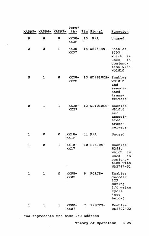
Port* XADR5- XADR4- XADR3- -1hl Pin Sisnal Function
111 111 111 XX38- 15 N/A Unused XX3F
111 111 1 XX 3 111- 14 W8253EN- Enables XX37 8253,
which is used in conjunc-tion with WD1010
1 111 XX28- 13 WD11111I11CS- Enables XX2F WD1010
and associ-ated trans-ceivers
1 1 XX20- 12 WDlI1110CS- Enables XX27 WDl010
and associ-ated trans-ceivers
1 111 '" XXl8- 11 N/A Unused XXIF
1 '" 1 XXl0- 10 8253CS- Enables
XX17 8253, which is used in conjunc-tion with WD2797-02
1 1 0 XX08- 9 FCRCS- Enables XX0F decoder
l2F during I/O write cycle (see below)
1 1 1 XX00- 7 2797CS- Enables XX 111 7 WD2797-02
*XX represents the base I/O address
Theory of Operation 3-25
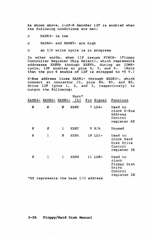
As shown above, 1-of-8 decoder l2F is enabled when the following conditions are met:
o XADR3- is low
o XADR4- and XADR5- are high
o an I/O write cycle is in progres~
In other words, when llF issues FCRCS- (Floppy Controller Register Chip Select), which represents addresses XX08h through XX0Fh, during an IOWRcycle, l2F enables at pins 4, 5, and 6. (Note that the pin 6 enable of l2F is strapped to +5 V.)
X-Bus address lines XADRl- through XADR3-, which connect at connector Jl, pins 84, 83, and 82, drive l2F (pins 1, 2, and 3, respectively) to output the following:
Port* XADR3- XADR2- XADRl-~ ~ Signal Function
0· XX0E 7 LD4-
1 XX0C 9 N/A
1 XX0A 10 LDl-
1 1 XX08 11 LD0-
*XX represents the base I/O address
3-26 Floppy/Hard Disk Manual
Used to clock X-Bus Address Control register 6E
Unused
Used to clock Hard Disk Drive Control register 3E
Used to clock Floppy Disk Drive Control register 2E
FLOPPY DISK DRIVE CONTROLLER LOGIC
INTRODUCTION
The WD2797-32 floppy disk formatter/controller (2C), shown in Figure 3-1, page 7, provides most of the circuitry necessary to control the floppy disk drive, including a phase-locked loop data separator, write precompensation circuitry, address mark generation and detection circuitry, and CRC circuitry. The WD2797-32 clock can operate at 1 MHz during read or write operations, or at 2 MHz to enable track ~eeks at 3 milliseconds per track. A functional block diagram of the floppy disk drive controller logic is provided in Figure 3-2. The pin assignments and functions for 2C are listed in Table 3-1.
Theory of Operation 3-27
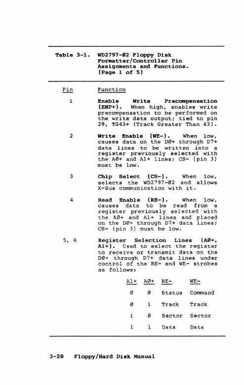
Table 3-1. WD2797-82 Floppy Disk Formatter/COntroller Pin Assignments and Functions. (Page 1 of 5)
Pin Function
1 Enable Write Precompensation (ENP+). When high, enables write precompensation to be performed on the write data output: tied to pin 29, TG43+ (Track Greater Than 43).
2 Write Enable (WE-). When low, causes data on the D0+ through 07+ data lines to be written into a register previously selected with the A0+ and Al+ lines: CS- (pin 3) must be low.
3 Chip Select (CS-). When low, selects the W02797-02 and allows X-Bus communication with it.
4 Read Enable (RE-). When low, causes data to be read from a register previously selected with the A0+ and Al+ lines and placed on the 00+ through .07+ data lines: CS- (pin 3) must be low.
5, 6 Register Selection Lines (M+, Al+). Used to select the register to receive or transmit data on the 00+ through D7+ data lines under control of the RE- and WE- strobes as follows:
Al+ A0+ RE- WE-
o 0 Status Command
o 1 Track Track
1 0 Sector Sector
1 1 Data Oata
3-28 Floppy/Bard Disk Manual
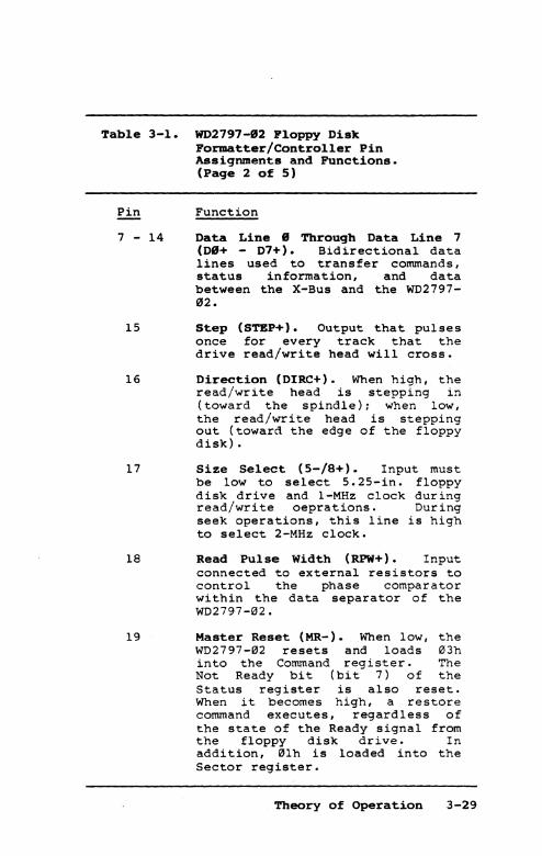
Table 3-1. WD2797-02 Floppy Disk Formatter/Controller Pin Assignments and Functions. (Page 2 of 5)
Pin Function
7 - 14 Data Line 0 Through Data Line 7 (D0+ - D7+). Bidirectional data lines used to transfer commands, status information, and data between the X-Bus and the WD2797-132.
lS Step (STEP+). Output that pulses once for every track that the drive read/write head will cross.
16 Direction (DIRC+). When high, the read/write head is stepping in (toward the spindle); when low, the read/write head is stepping out (toward the edge of the floppy disk) •
17 Size Select (5-/8+). Input must be low to select S.2S-in. floppy disk drive and l-MHz clock during read/wri te oeprations. Dur ing seek operations, this line is high to select 2-MHz clock.
18 Read Pulse Width (RPW+). Input connected to external resistors to control the phase comparator within the data separator of the WD2797-132.
19 Master Reset (MR-). When low, the WD2797-02 resets and loads 03h into the Command register. The Not Ready bit (bit 7) of the Status register is also reset. When it becomes high, a restore command executes, regardless of the state of the Ready signal from the floppy disk drive. In addition, 0lh is loaded into the Sector register.
Theory of Operation 3-29
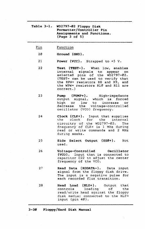
Table 3-1. WD2797-82 Floppy Disk Formatter/Controller Pin Assignments and Functions. (Page 3 of 5)
Pin Function
20 Ground (GND).
21 Power (VCC). Strapped to +5 V.
22 Test (TEST-). When low, enables internal signals to appear on selected pins of the WD2797-02. (TEST- can be used to verify that the RP\H resistors R8 and R9, and the WPW+ resistors R10 and Rll are correct.)
23 Pump (PUMP+). High-impedance output signal, which is forced high or low to increase or decrease the vol tage-controlled oscillator (veo) frequency.
24 Clock (CLK+). Input that supplies the clock for the internal circuitry of the WD2797-02. The frequency of CLK+ is 1 MHz during read or write commands and 2 MHz during seeks.
25 Side Select Output (SS8+) • used.
Not
26 Voltage-Controlled Oscillator (vea). Input that is connected to capacitor C22 to adjust the center frequency of the VCO.
27 Read Data (RDDATA-). Data input signal from the floppy disk drive. The input is a negative pulse for each recorded flux transition.
28 Head Load (HLD+). Output that controls loading of the read/write head against the floppy disk media; connected to the HLT+ input (pin 40).
3-38 Floppy/Bard Disk Manual
Table 3-1. WD2797-82 Floppy Disk Formatter/Controller Pin Assignments and Functions. (Page 4 of 5)
Pin Function
29 Track Greater than 43 (TG43+).
3117
Output that informs the floppy disk drive when the read/write head is positioned between tracks 44 through 76: valid only during a read or write command.
Write Gate (WG+). valid before data the floppy disk.
Output that is is written on
31 Write Data (WRDATA+). Output that issues a 250-nsec (MFM) pulse for each flux transition written on the floppy disk: contains the unique address marks as well as data and clocks for the floppy disk drive.
32 Ready (READY+). Input that indicates floppy disk drive readiness: sampled for a high state before read or write commands are performed. If low, the read or write command is not performed, and an interrupt is generated. Type 1 commands are performed regardless of the state of READY+. (See Section 2, "Architecture. " ) The READY+ input appears in inverted format as Status register bit 7.
33 Write Precompensation Width (WPW+). External resistors tied to this input control the amount of delay in the write pre~ompensation mode.
34 Track 117" (TR00- ) • Input from the floppy disk drive, indicating that the read/write head is over track 117117.
Theory of Operation 3-31
Table 3-1. WD2797-82 Floppy Disk Formatter/Controller Pin Assignments and Functions. (Page 5 of 5)
Pin Function
35 Index Pulse (IP-). Input from the floppy disk drive, indicating that the index hole on the floppy disk has been encountered.
36 Write Protect (WPRT+). Input sampled whenever a write command is received by the WD2797-02 A low at this input terminates the write command and sets the writeprotect bit in the Status reg ister • (See Section 2, "Architecture.")
37 Double Density (MFM+). Input tied to ground, selecting double
3-32
density (MFM) encoding of data.
38 Data Request (DRQ+). Output indicating that the Data register of the WD2797-02 contains asembled data in read operations, or the Data register is empty in write operations. This signal is reset when serviced by the Processor Module through reading or loading of the Data register. (See Section 2, "Architecture.")
39 Interrupt Request (INTRQ+). Output that is set at the completion of any command and is reset when the Status register is read from or the Command register is written to. (See Section 2, "Architecture.")
40 Head Load Timing (HLT+) • Connected to the HLD+ output (pin 28) of 2C to control the head load timing.
Floppy/Hard Disk Manual
From 8253
From Floppy
Disk Drive
From Module
Data Bus Interface
Logic
From X-Bus Master
From X-Bus
Data Bus Interface
Logic
{ )
{
\
TRACKOO-
WRPROT-
INDEX-
READY-
~
MDO+-MD7+
" /
XADR1--XADR5-
lORD-
lOWR-
00+-07+
" -V
4/
) / I WD2797-02
Floppy Disk Formatter/ Controller
2C -CLK<
lMHz/2MHz
Reset
2/ Floppy Disk /
Drive Control Register
2E
lE XINTR5-
lE XDR04-
WRDATA-
WRGATE-
STEP-Buffer
10 DIR-
[>0 DSO-
MOTOR-
RDDATA-
SIDESEL-
4E
} -
I-
-
To X-Bus Master
To Floppy Disk Drive
To Floppy Disk Drive
3-2. Floppy Disk Controller Logic Functional Block Diagram.
Theory of Operation 3-33
GENERAL OPERATION
As shown in Figure 3-1, page 7, the WD2797-02 formatter/controller, shown as 2C, is enabled at pin 3 when IlF generates 2797CS- from pin 7, signifying addx:.esses XX1313h through XX07h. (See "Floppy/Hard Disk Module Device Decoding," above.) When 2C is selected, the X-Bus master can select one of several registers by using XADR1- and XADR2- X-Bus address lines and can read from, or write to, the selected register by using the XDAT13- through XDAT7- lines to transfer data. (See "X-Bus Data Interface," above.) XADR1- is inverted at pin 14 of 7F before generating to 2C (pin 5) as A0+. XADR2- is inverted at 7F (pin 12) before generating to 2C (pin 6) as Al+.
Read operations are indicated when XIORDgenerates through pin 3 of buffer l0F (Figure 3-1, page 2) to the RE- (Read Enable) input of 2C at pin 4, shown in Figure 3-1, page 7. Similarly, write operations are indicated when XIOWRgenerates through pin 5 of l0F (Figure 3-1, page 2) to the WE- (Write Enable) input of 2C at pin 2. Internal registers of 2C are listed below with their addresses in the module relative to the module base I/O address, XXh:
Read Register Write Register Al+ A0+ (RE- ) (WE-)
0 13 Status (XX130h) Command (XX00h)
0 1 Track (XX02h) Track (XX02h)
1 13 Sector (XX134h) Sector (XX04h)
1 1 Data (XX06h) Data (XX06h)
When the X-Bus master performs a read or write operation to the floppy disk drive, it writes data into the WD2797-02 (2C) Sector and Track registers and then writes the command byte into the Command register. If a read operation is commanded, 2C assembles a serial byte from the floppy disk drive, loads it into the Data register, and sets the DRQ+ (DMA Request) line at pin 38 high (as shown in Figure 3-1, page 7). DRQ+ is inverted at NAND gate IE and sent to the X-Bus master to request service as XDRQ4- (X-Bus DMA Request, Priority 4) via connector Jl, pin 59. The X-Bus master reads the Data register at address XX06h
Theory of Operation 3-35
for the byte. This continues for all bytes requested in the command.. When the command has been completed, 2C interrupts the X-Bus master through its INTRQ+ (Interrupt Request) line at pin 39. INTRQ+ is inverted at pin 8 of NAND gate IE and sent to the X-Bus master as XINTR5- (X-Bus Interrupt, Priority 5) via c~nnector Jl, pin 114, to request a new command sequence. Finally, as shown in Figure 3-1, page 6, the X-Bus master sets XDMAEN- high again, to signify that a DMA cycle is not in progress.
A write to the floppy disk drive occurs in the same manner, except that DRQ+ is set when 2C requires a byte from the X-Bus master. Again, 2C requires a byte from the X-Bus master when it has completed the command.
FLOPPY DISK DRIVE CLOCK LOGIC
Data bit 6 of the Floppy Disk Drive Control register (2E in Figure 3-1, page 7), controls the frequency of the 1- or 2-MHz clock used to control operations of the WD2797-02 shown as 2C. If data bit 6 is set, MUX- (Multiplex) becomes high before it is multiplexed at 7B (Figure 3-1, page 4) to produce a 2-MHz FPCLK- (Floppy Clock) at pin 6. If data bit 6 is reset, MUX- is inverted at pin 12 of 9A before it is multiplexed at 7B to produce a I-MHz FPCLK- at pin 6. FPCLK- is generated to pin 24 of 2C as shown in Figure 3-1, page 7.
Note in Figure 3-1, page 4, that the 2-MHZ+ pulse is generated by 4-bit binary counter 70 (pin 10). Counter 70 is clocked by a l0-MHz pulse (pin 13), which originated at 20-MHz oscillator l0A. The 2-MHz pulse is divided by two at D flip-flop 9B (pin 5), generating lMHZ+.
FLOPPY DISK DRIVE INTERFACE LOGIC
The interface between the WD2797-02 formatter/controller and the floppy disk drive consists of a Floppy Disk Drive Control register for drive selection, motor control, and clock pulses, and of one buffer for data and control signals.
3-36 Floppy/Bard Disk Manual
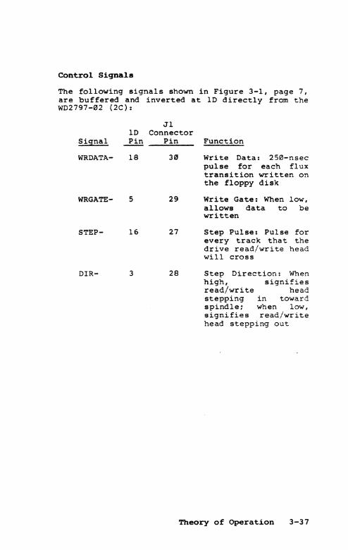
Control Signals
The following signals shown in Figure 3-1, page 7, are buffered and inverted at ID directly from the WD2797-02 (2C):
Jl ID Connector
Signal ~ Pin Function
WRDATA- 18 3111 Write Data: 250-nsec pulse for each flux transition written on the floppy disk
WRGATE- 5 29 Write Gate: When low, allows data to be written
STEP- 16 27 Step Pulse: Pulse for every track that the drive read/write head will cross
DIR- 3 28 Step Direction: When high, signifies read/write head stepping in toward spindle; when low, signifies read/write head stepping out
Theory of Operation 3-37
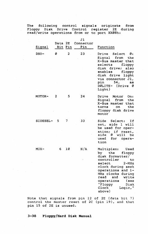
The following control signals originate from Floppy Disk Drive Control register 2E during read/write operations from or to port XX08h:
Signal Data 2E Bit Pin
DSO- 0 2
MOTOR- 2 5
SIDESEL- 5 7
MUX- 6 10
Jl Connector
Pin
23
24
33
N/A
Function
Drive Select 0: Signal from the X-Bus master that selects floppy disk drive~ also enables floppy disk drive light via connector Jl, pin 54, as D0LITE- (Drive 0 Light)
Drive Motor On: Signal from the X-Bus master that turns on the floppy disk drive motor
Side Select: If set, side 1 will be used for operation ~ if reset, side 0 will be used for operation
Multiplex: Used by the floppy disk formatter/ controller to select 2-MHz clock during seek operations and 1-MHz clocks during read and write operations (see "Floppy Disk Clock Logic," above)
Note that signals from pin 12 of 2E (data bit 7) control the master reset of 2C (pin 19), and that pin 15 of 2E is unused.
3-38 Floppy/Hard Disk Manual
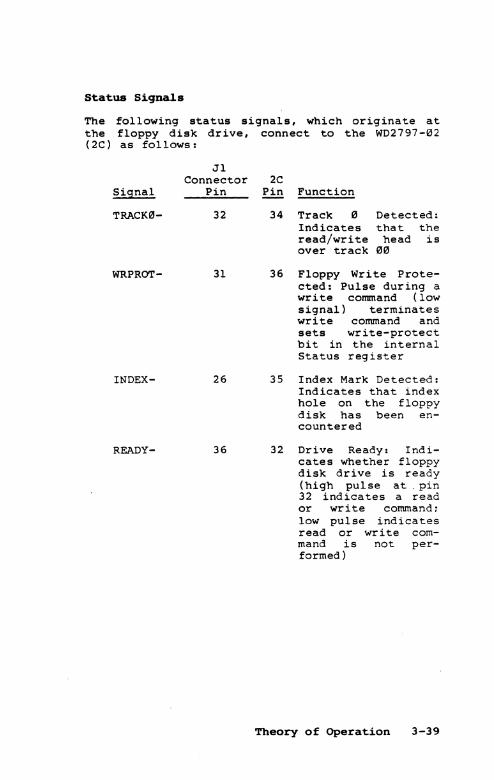
Status Signals
The following status signals, which originate at the floppy disk drive, connect to the WD2797-12l2 (2C) as follows:
Signal
TRACKI2l-
WRPROT-
INDEX-
READY-
Jl Connector 2C
Pin Pin Function
32
31
26
36
34 Track Detected: Indicates that the read/write head is over track I2lIll
36 Floppy Write Protected: Pulse during a write command (low signal) terminates write command and sets write-protect bit in the internal Status register
35 Index Mark Detected: Indicates that index hole on the floppy disk has been encountered
32 Drive Ready: Indicates whether floppy disk drive is ready (high pulse at. pin 32 indicates a read or write command; low pulse indicates read or write command is not performed)
Theory of Operation 3-39
HARD DISK DRIVE CONrROLLER LOGIC
INrRODUCTIOH
The hard disk drive controller circuitry in the Floppy/Hard Disk Module is built around the WD1~1~ Winchester disk controller (12C) shown in Figure 3-1, page 2, which provides the following:
o multiple sector read/write commands
o CRe generation/verification circuitry
o data rates up to SM bits per second (bps)
o automatic restore on seek errors
A functional block diagram of the hard disk drive controller logic is provided in Figure 3-3. The pin assignments and functions of l2C are listed in Table 3-2.
3-48 Floppy/Bard Disk Manual
From Hard Disk Drive
Control Register 3E
To/From 8263
From Clock Generation
logic
To X-Bus To X-Bu.
Elltendod Addren Regi .... To X-Bus
Master
To/From X-Bu.
From PAL 7E From Module DltVice
OecorIing Logic
BooTEN-
Control.
2MH.
~ ~ Bul,",
~ 4E
... XDATO--XDATF- ..
< DSBLRW+
STARn
WD101OCS-
From { X-Bus Master
IORD-
IOWR-
From X-au. Master
XADR1--XADRS-
State Sequencer
logic 58,6B
I
X-Bu. Da ..
Interface
...
BAI)<--BAB+ ~ Counter logic
J 7A, 80, 70
1 Controls
2732 PALs r--EPROM e- 7E
7C 13E Controls CE
1 ~ .J r ~
Enable Module
Qata au. Interface
logic
RAM Data Buffer
BAI)<--BAA+
I Enables 6331-1
J.c]s I EPROM
8B
I-t. -" 8K-Byte RAM
Data Buff. ec,9C,
IOC,IIC
I Controls
Hard Disk Driwt
RaodlWrite Logic
4/ /
FromMFM aa .. Con .... on
ToWFM Data/Clock Connectors
01)<-1 A 07+ Interface Vt--
Logic
" OO+-DF+ 9O,1DD, 11E,11O
4E
~ Enable
Bul,", 10F
r--
From Hard Disk Drive y
00.-07. "
WDI)<--WD7+ 5MH.
WD10l0 Winchester
Enable Disk Controller
12C
TKO+
Buff .. SC+ 12E DRDY+
1>0 WF+
lOX' R_
Bul,", 2j 3F
Hard Disk I Drive 1>0 3/ Control
Register I 3E
I
Clock Generation
logic
9A INTR2-V
2/ STEP-Buffer 2/7 ... 4F DIR-
F 2/ RWC-
1>0 2/ I WRGT-
DSEL-
3/ EHSEL-
/ HSEL-
BOOTEN., _RITE.
_J'.,60 BOOTEN
To X-Bus Master
}TO Hard Disk Drive
To PAL. To 2732 EPROM 7C
Hard Disk Controller Logic Functional Block Diagram.
Theory of Operation 3-41

Table 3-2. WDl818 Winchester Disk Controller Pin Assignments and Functions. (Page I of 3)
~ Function
1 Buffer Chip Select (BCS-) • Active-low output used for selecting external RAM data buffer.
2 Unused.
3 Interrupt Request (INTRQ+). Output that is set high at the completion of any command.
4 Must be an open circuit.
5 Master Reset (MR-). Input used '1...0 intialize all internal logic.
6 Read Enable (RE-). Bidirectional line used as an input for reading the Task registers and an output when l2C reads the RAM data buffer: tristate.
7 Write Enable (WE-). Bidirectional line used as an input for writing into the Task registers and as an output when l2C writes to the RAM data buffer: tristate. •
8 Chip Select (CS-). Used to enable l2C.
9 - 11
12 - 19
20
Address Lines (Ml+ Through A2+). Used to select the internal register to transmit/receive data on the D0+ through D7+ data bus.
Data Bus (D8+ Through D7+). Bidirectional bus used to trans fer commands, status information, and data.
Ground.
Theory of Operation 3-43
Table 3-2. WD1BIe Winchester Disk Controller Pin Assignments and Functions. (Page 2 of 3)
Pin
21
22, 23
24
25
26
27
28
29
30
31
Function
Write Data (WD+). Output that contains the MFM clock and data pulses to be written on the disk.
Unused.
Write Gate (WG+). Output set high before a write is performed on the disk.
Write Clock (WC+). 5-MHz clock input used to derive internal write timing.
DIR+ (Direction). Output that determines the direction of the stepping motor.
Step Pulse (STEP+). Output pulses used for the stepping motor.
Drive Ready (DRDY+). Input that must be high to allow the execution of commands.
Index Pulse (IDX+). Input that informs 12C when the index hole has been encountered.
Write Fault (WF+). 12C that indicates dition at the drive.
Error' input to a fault con-
Track eee (TK0+). Input that indicates the read/write heads are positioned over the outermost cylinder.
32 Seek Complete (SC+). Input that informs 12C when head settling time has expired.
3-44 Floppy/Hard Disk Manual
Table 3-2. WD1S1S Winchester DisK Controller Pin Assignments and Functions. (Page 3 of 3)
Pin Function
33
34
35
36
Reduced Write Current (RWC+) • Programmed output used to reduce write current on a selected starting cylinder.
Data Run (DRUH+). Input that informs 12C when a string of ls or 0s has been detected.
Buffer Ready (BRDY+). Input that informs 12C that the sector RAM data buffer is full or empty.
Buffer Data Output set to fers to/from buffer.
Request (BDRQ+). initiate data transthe sector RAM data
37 Read Data (RD+). Input from the hard disk drive; consists of both MFM clocks and data pulses.
38 Read Gate (RG+). Output set high when data is being inspected from the hard disk.
39 Read ClOCK (RCLK+). Square-wave clock input derived from the external data recovery circuits.
40 Power (+5 V). Power supply input.
GENERAL OPERATION
The WD1010 (12C) controls the hard disk drives in both the Floppy/Hard Disk Module and the Hard Disk Expansion Module.
The X-Bus master selects 12C via 1-of-8 decoder llF (Figure 3-1, page 7) as described in the "Floppy/Hard Disk Module Device Decoding"
Theory of Operation 3-45
subsection, above. A low signal at pin 12 of llF (representing addresses XX20h through XX27h) is inverted at pin 16 of 7F and NORed at gate 6A to generate WD10l0CS- at pin 4. Note that a low signal at pin 13 of llF (representing addresses XX2Bh through XX2Fh) is inverted at pin 9 of 6D and also forces NOR gate 6A (pin 4) low as WD10l0CS-.
As shown in Figure 3-1, page 2, WD10l0CS- is buffered at tristate buffer l0F, which is enabled at pin 1.
A disk operation begins when the X-Bus master writes task information into the Task registers of l2C. (See Section 2, "Architecture," for task information.) After the task information has been written, the X-Bus master writes the command into the Command register. During a write sector command, the X-Bus master can then read the status of l2C to inspect the buffer data request flag, and write data into the RAM data buffer. (See the "Hard Disk Drive Controller RAM Data Buffer" subsection, below.)
When the RAM data buffer becomes full, it activates the BRDY+ (Buffer Ready) input of l2C. Then, l2C de-asserts the BDRQ+ (Buffer Data Request) line and asserts BCS- (Buffer Chip Select) allowing l2C to have a direct bus to the RAM data buffer, which is isolated from the X-Bus read/write control lines. The X-Bus data bus cannot access l2C (because of tristate buffer l0F). When the buffered data is transferred to the hard disk, and the RAM data buffer is empty, START+ enables tristate buffer l0F, thereby recQ.nnecting the two buses. The X-Bus can then read or write status/commands from or to l2C.
DISABLE READ/WRITE
The X-Bus master uses DSBLRW+ (Disable Read/Write) to disable the X-Bus read/write control lines to l2C so that these lines do not interfere with the read/write signals of l2C, which are used for incrementing the RAM data buffer. (See the "RAM Chip Selection and Addressing" subsection, below.)
As shown in Figure 3-1, page 4, the X-Bus master sets data bit 7 of X-Bus Extended Address register 6E (port XX0Eh) to generate DSBLRW+ from pin 2.
3-46 Floppy/Bard Disk Manual
As shown in Figure 3-1, page 2, DSBLRW+ is inverted at pin 14 of 4E and NORed with an inactive START+ at gate 6A (pins 9 and 8, respectively), generating a high signal at pin 10, which disables buffer 10F at pin 1. (An inactive START+ signifies that a DMA cycle is not in progress. )
HARD DISK DRIVE CLOCK LOGIC
As shown in Figure 3-1, page 4, the reference clock for the hard disk drive read and write circuitry is a 20-MHz crystal oscillator, l0A. It clocks J-K flip-flop l0B (pin 1) to generate a 10-MHz frequency at pin 5. This l0-MHz signal is used at multiplexer llA (pin 2) as a 10-MHz phaselocked loop reference when RG+ (Read Gate) at pin 38 of the WD1010 (12C) is not asserted. (See the "Hard Disk Drive Read/Write Circuitry" subsection, below. )
In addition, this l0-MHz frequency is divided by two at J-K flip-flop 10B (pin 9) ~s a 5-MHz pulse, which is used to derive internal write timing at 12C (pin 25).
A 10-MHz signal is also generated from pin 6 of 10B to pin 11 of D flip-flop IF for use with the MFM clock/data output to driver 2F.
Four-bit binary counter 7D is used to divide the 10-MHz signal down to a 2-MHz pulse at pin 10. This 2-MHz pulse clOCKS counter 2 of 8253 programmable interval timer 5C (shown in Figure 3-1, page 5), which is .used to count the time elapsed after one DMA burst. In addition, 2MHZ+ is used to clOCK the state sequencer chips 5B and 6B. (See the "State Sequencer" subsection, below. )
HARD DISK DRIVE INTERFACE LOGIC
The applicable hard diSK drive is selected when the X-Bus master writes to port XX0Ah as described in the "Floppy/Hard DiSK Drive Module Device Decoding" subsection. As shown in Figure 3-1, page 7, LD1- (Load 1) is generated from pin 10 of 1-of-8 decoder 12F when the X-Bus master writes to address XX0Ah. LD1- clocks Hard Disk Drive Control register 3E at pin 11 (See Figure 3-1,
Theory of Operation 3-47
page 3), to generate signals through buffer 3F, which is enabled at pins 1 and 19. Note that 3F inverts the signals connecting from 3E.
Control Signals
The control data bits written to 3E and the corresponding output functions at connector Jl are as follows:
Data !ll.L
1
3
4
Jl Connector
Signal Pin
DSEL0- 3
DSEL1- 47
HSEL0-/ 9 EHSEL0- 48
HSEL1-/ 10 EHSELl- 46
Function
Drive Select 0: Signal from the X-Bus master that selects the Floppy/Hard Disk Module hard disk drive
Drive Select 1: Signal from the X-Bus master that selects the Expansion Module hard disk drive
Head Select 0/ Expansion Head Select 0: Signal from the X-Bus master that selects either Floppy/Hard Disk Module hard disk head 0 or Expansion Module hard disk head 0 (depending on data bits 0 and 1)
Head Select 1/ Expansion Head Select 1: Signal from the X-Bus master that selects either Floppy/Hard Disk Module hard disk head 1 or Expansion Module hard disk head 1 (depending on data bits 0 and 1)
3-48 Floppy/Hard Disk Manual
Data ~
5
Jl Connector
Signal Pin
HSEL2-/ 16 EHSEL2- 47
Function
Head Select 2/ Expansion Head Select 2: Signal from the X-Bus master that selects either Floppy/Hard Disk Module hard disk head 2 or Expansion Module hard disk head 2 (depending on data bits ~ and 1)
Data bits written to 3E to perform other functions are as follows:
Data Bit Signal
2 BOOTEN-/ BOOTEN+
6 WWRITE+
7 l0l0RST-
Function
Used to enable boot P.DM
Used to activate BRDY+ input to the WD10l0, indicating a hard disk write operation is in progress
Initializes all internal logic of the WD10l0
The Hard Disk Drive Control register is disabled via DISBL- (Disable), which is generated from PAL 7E at pin 14, shown in Figure 3-1, page 5. (See the "Programmable Array Logic" subsection il'1 Section 2, "Architecture," for programming information on 7E.)
Theory of Operation 3-49
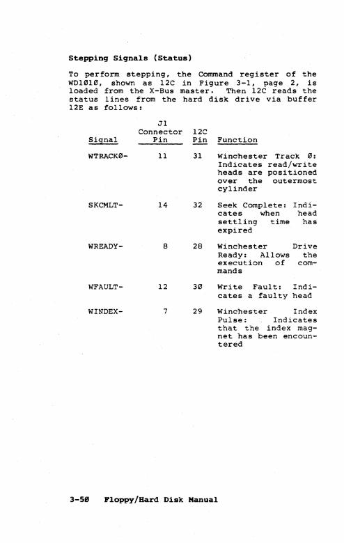
Stepping Signals (Status)
To perform stepping, the Command register of the WD10l0, shown as l2C in Fi9ure 3-1, page 2, is loaded from the X-Bus master. Then l2C reads the status lines from the hard disk drive via buffer l2E as follows:
Jl Connector 12C
Si~nal Pin Pin
WTRACK0- 11 31
SKCMLT- 14 32
WREADY- 8 28
WFAULT- 12 30
WINDEX- 7 29
Function
Winchester Track 0: Indicates read/write heads are positioned over the outermost cylinder
Seek Complete: Indi-cates when head settling time has expired
Winchester Drive Ready: Allows the execution of com-mands
Write Fault: Indicates a faulty head
Winchester Index Pulse: Indicates that the index magnet has been encountered
3-5" Ploppy/Hard Disk Manual
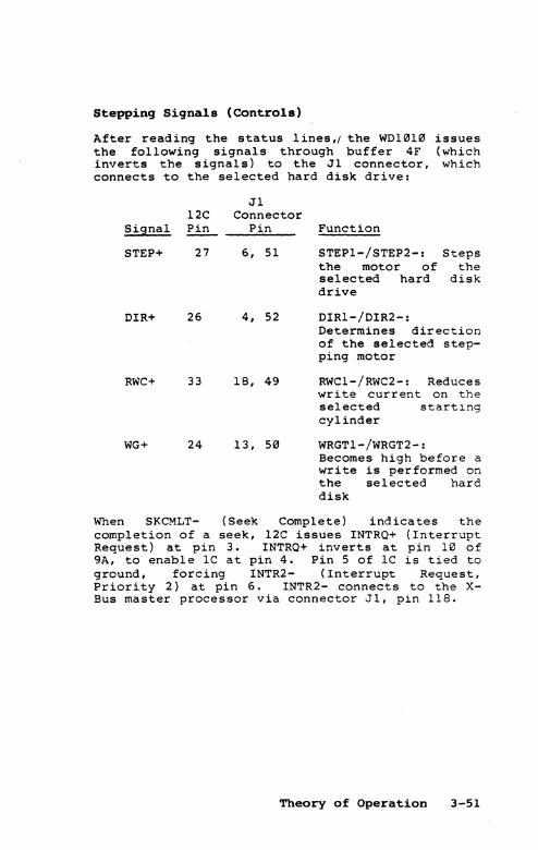
Stepping Signals (Controls)
After reading the status lines,( the WDl0Hl the following signals through buffer 4F inverts the signal s) to the J 1 connector, connects to the selected hard disk drive:
issues (which which
Jl l2C Connector
Signal Pin Pin Function
STEP+ 27 6, 51 STEPl-/STEP2-: Steps the motor of the selected hard disk drive
DIR+ 26 4, 52
RWC+ 33 18, 49
WG+ 24 13, 50
DIR1-/DIR2-: Determines direction of the selected stepping motor
RWCl-/RWC2-: Reduces write current on the selected start~ng
cylinder
WRGTl-/WRGT2-: Becomes high before a write is performed on the selected hard disk
When SKCMLT- (Seek Complete) indicates the completion of a seek, l2C issues INTRQ+ (Interrupt Request) at pin 3. INTRQ+ inverts at pin 10 of 9A, to enable lC at pin 4. Pin 5 of IC is tied to ground, forcing INTR2- (Interrupt Request, Priori ty 2) at pin 6. INTR2- connects to the XBus master processor via connector JI, pin 118.
Theory of Operation 3-51
HARD DISK DRIVE BOOT ROM
As shown in Figure 3-1, page 2, 4K-byte EPROM 7C contains the necessary inforTTl'=!1::i_0n for the X-Bus master to boot from the hard disk drive.
The X-Bus master accesses 7C by setting data bit 2 of Hard Disk Drive Control register 3E (port XX0Ah) shown in Figure 3-1, page 3. BOOTEN+ (Boot Enable) is inverted as BOOTEN- at pin 18 of 6D and driven to pin 18 of 7C, shown in Figure 3-1, page 2, enabling 7C.
During a DMA cycle, the X-Bus master issues an IORD- to pin 20 of 7C, enabling the output of D0+ through D7+.
In addition, BOOTEN+ is generated to PAL 7E at pin 7 (Figure 3-1, page 5), and- IORD- is generated to 7E (pin 3), causing 7E to generate ADRINC+ (Address Increment), which causes address counters 8D and 7D to increment (Figure 3-1, page 6). Buffered address lines BA0+ through BAB+ are generated to 7C (Figure 3-1, page 2).
HARD DISK DRIVE CONTROLLFR RAM DATA BUFFER
The RAM data buffer consists of four blocks of 2K by 8 bits (2K bytes) of static RAM, totaling 8K bytes. As shown in Figure 3-1, page 3, and Figure 3-4, two blocks consist of even-numbered low-order bytes (llC and l0C), and two blocks consist of odd-numbered high-order bytes (9C and 8C). Power feeds into the RN1 chips at pin 24, and each chip is grounded at pin 12.
Buffered address lines BA0+ through BAA+ are input at pins 1 through 8 and 19, 22, and 23. (See the "RAM Chip Selection and Addressing" subsection, below.) Data input/output lines are connected to pins 9 through 11 and 13 through 17. Ei ther the X-Bus master or the WD10l0 pulses pin 21 as WDIOWR- to enable a write or pin 20 as WDIORD- to enable a read. The chip selects (pin 18) are controlled by 6331-1 PROM 8B, shown in Figure 3-1, page 6. (See Table 3-3 for the input and output functions of 8B.)
3-52 Floppy/Hard Disk Manual
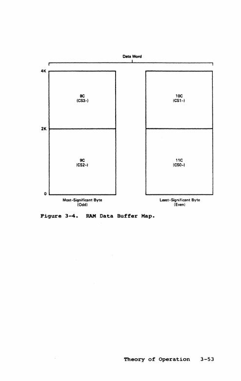
4K r----------.....,
BC ICS3-)
2K ~--------~
9C ICS2-)
O~ ____________ ~
Most-Significant Byte IOdd)
Data Word
10C ICSH
11C ICSO-)
Least-Significant Byte IEven)
Figure 3-4. RAM Data Buffer Map.
Theory of Operation 3-53
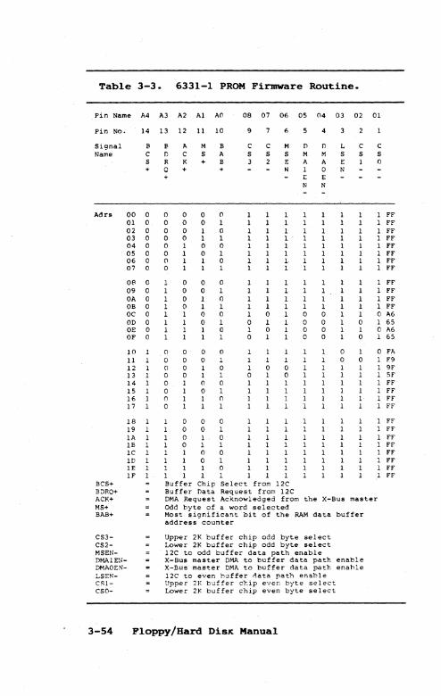
Table 3-3. 6331-1 PROM Firmware Routine.
Pin Name A4 A3 A2 Al An 08 07 06 05 n4 03 02 01
pin No. 14 13 12 11 10 9 6 4
Signal B B A M B C C M fl fl L e e Name e fl e S A S S S M M S S S
S R K + B 3 2 E A A E 1 ()
+ Q + + N 1 0 N + E E
N N
Adrs 00 0 0 0 0 0 1 FF 01 0 0 0 0 1 1 FF 02 0 0 0 1 0 1 FF 03 0 0 0 1 1 1 FF 04 0 0 1 0 0 1 FF 05 0 0 1 0 1 1 FF 06 0 0 1 1 0 1· FF 07 0 0 1 1 1 1 FF
08 0 0 0 0 FF 09 0 0 0 1 FF OA 0 0 1 () 1 1 1 1 1 FF DB 0 0 1 1 1 1 1 1 1 FF OC 0 1 0 0 0 0 0 1 0 A6 OD 0 0 1 0 1 0 0 0 1 65 OE 0 1 0 1 0 0 0 1 0 A6 OF 0 1 1 0 1 0 0 0 1 65
10 n 0 0 0 1 0 1 0 FA 11 0 0 0 1 1 1 1 0 0 1 F9 12 0 0 1 0 1 0 0 1 1 9F 13 0 0 1 1 0 1 0 1 1 SF 14 0 1 0 0 1 1 1 1 1 FF 15 0 1 0 1 1 1 1 1 1 FF 16 0 1 1 0 1 1 1 FF 17 0 1 1 1 1 1 1 FF
18 0 0 0 FF 19 0 0 1 FF III 0 1 0 FF IB 0 1 1 FF Ie 1 0 0 FF ID 1 0 1 FF IE 1 1 0 FF IF 1 1 1 FF
BCS+ Buffer Chip Select from 12C B;)RQ+ Buffer Data Request from 12C ACK+ DMA Request Acknowledged from the X-Bus master MS+ Odd byte of a word selected BlIB+ Most significant bit of the RAM data buffer
address counter
CS3- Upper 2K buffer chip odd byte select CS2- Lower 2K buffer chip odd byte select MSEN- 12C to odd buffer data path enable flMAIE:l- X-Bus master DMA to buffer data path enable DMAOE~- X-Bus master DMA to buffer data path enahle LSEN- 12C to even huffer nata path enable CS1- Upper 2K buffer c~ip even byte se 1 eet CSO- Lower 2K buffer chip even byte select
3-54 Floppy/Hard DisK Manual
RAM CHIP SELECTION AND ADDRESSING
When the WD11IJ11IJ (12C) is reading from or writing to the RAM data buffer, BCS- (Buffer Chip Select) is inverted at pin 3 of l2E (Figure 3-1, page 2) and driven as BCS+ to pin 14 of 8B (Figure 3-1, page 6). This causes 8B to generate CSIIJ- (Chip Select IIJ) from pin 1. As shown in Figure 3-1, page 3, CSIIJ- enables RAM data buffer llC at pin 18, which represents the least-significant, or even, data byte. In addition, 8B (Figure 3-1, page 6) generates LSEN- (Least Significant Byte Enable) from pin 3, enabling transceiver lID at pin 19 (Figure 3-1, pge 3), which allows WD0+ through WD7+ data transfers.
Before the next byte is generated, CNTRINCR(Counter Increment) is issued from PAL 7E (pin 15), shown in Figure 3-1, page 5. (See the "Programmable Array Log ic" subsection in Section 2, "Architecture," for programming information of PAL 7E.) CNTRINCR- clocks D flip-flop 7A (Figure 3-1, page 6), which acts as a state machine to generate two states for even and odd bytes. ODD+ (Odd Byte) is generated from 7A (pin 9) to 8B (pin 11) I causing 8B to issue CS2- from pin 7. As shown in Figure 3-1, page 3, CS2- enables RAM data buffer 9C (pin 18), which represents the mostsignificant (odd) byte. In addition, 8B (Figure 3-1, page 6) generates MSEN- (Most Significant Byte Enable) from pin 6, enabling transceiver IIlJD at pin 19 (Figure 3-1, page 3), which also allows WDIIJ+ through WD7+ data transfers.
During a write to the RAM data buffer, this sequence occurs for each data word until RAM data buffer chips llC and 9C become full (that is, contain 2K words). Four-bi t binary counters 8D and 7D shown in Figure 3-1, page 6, are used to detect the 2K-word limit. Every word causes 8D to increment by one count via ADRINC+, which is generated by PAL 7E at pin 16 (Figure 3-1, page 5). (See the "Programmable Array Logic" subsection in Section 2, "Architecture, " for programming information of PAL 7E.) When a 2K count is reached, represented by BAB+ at pin 6 of 7D, BAB+ is generated to pin 10 of 8B, causing 8B to issue CSl- from pin 2, representing the leastsignificant byte, and then CS3- from pin 9, representing the most-significant byte, in the same manner as described for CSIIJ- and CS2-, above. This allows for data words between 2K and 4K.
Theory of Operation 3-55
Note in Table 3-3 that the WDHH0 (12C) issues BDRQ+ (Buffer Data Request) from pin 36 (Figure 3-1, page 2) to pin 13 of 8B (Figure 3-1, page 6) to initiate the 8-bit data transfers to or from the RAM data buffer. In addition, ACK+ is issued as an acknowledge from the X-Bus master via connector Jl, pin 57, shown in Figure 3-1, page 5, as XDACK3-.
As shown in Figure 3-1, page 6, BDRQ+ and ACK+ are used at 8B when the X-Bus master transfers data to or from the RAM data buffer, since the X-Bus master transfers 2-byte data words (that is, 16 bits). An X-Bus master data transfer causes 8B to issue either DMA0EN- (DMA 0 Enable) from pin 4 or DMAlEN- (DMA 1 Enable) from pin 5. DMA0ENenables transceiver lIE (pin 19) to trans fer the least-significant data byte (D0+ through D7+). DMAlEN- enables transceiver 9D (pin 19) to transfer the most-significant data byte (D8+ through DF+).
3-56 Floppy/Hard Disk Manual
RAM DATA DIRECTION
When reading data, WDIORO- (at pin 1 of each transceiver shown in Figure 3-1, page 3) causes the following, depending upon the enables at pin 19:
o HID and IlD direct hard disk controller lines W00+ through WD7+ to the RAM buffers (since W01010 actually reading the hard disk and writing to the RAM buffers).
data data from data
o 90 directs data from the RAM data buffer lines to local data lines 08+ through OF+.
o lIE directs data from the RAM data buffer lines to local data lines 00+ through 07+.
When writing data, WDIORO- becomes inactive at pin 1 of each transceiver to cause the following, depending upon the enables at pin 19:
o 100 and IlD data from the RAM data buffer lines to hard disk controller data lines WD0+ through WD7+ (since the WD1010 is actually reading from the RAM data buffers and writing to the hard disk).
o 9D directs local data lines 08+ through OF+ to RAM data lines.
o lIE directs local data lines 00+ through 07+ to RAM data lines.
Theory of Operation 3-57
DIRECT MEMORY ACCESS TRANSFERS
The 8253 programmable interval timer (5C) shown in Figure 3-1, page 5, is used to determine DMA transfer word counts.
counter 0 is used to count the number of words being transferred to the X-Bus master. Counter 0 will interrupt on the last count by issuing END+ from pin 10 of 5C, signaling the DMA counter to start. Counters 1 and 2 are used as pulses for DMA. Counter 1 contains the number of words required for the DMA count (that is, burst size), and counter 2 is used as a time delay before the next DMA pulse to avoid bus contention. (See the "8253 Programmable Interval Timers" subsection, below, for 8253 operation, and the "State Sequencer" subsection, below, for states of the DMA transfers.)
For proper read/write sector and format timing, see the following:
0 Figure 3-5, "Read/Write Sector Timing Diagram"
0 Figure 3-6, "Single Sector Read Timing Diagram"
0 Figure 3-7, "Single Sector Write Timing Diagram"
3-58 Floppy/Hard Disk Manual
START (7E-12)
END (SC-10)
END2 (4C-17)
BCSR (13E-15)
BORa (12C-36)
8253CLK (WD1010
Read or Write) (7E-19)
INTR2 (WD1010)
(12C-3)
DMACLK 17E-17)
Write 8 Sectors Read 8 Sectors
Ii
--u '--__ --II
~~ ______ ~!l~~
UIJllIlIJ IJUlIllIJ
Conditions: Triggered on START
Figure 3-5. Read/Write Sector Timing Diagram.
Theory of Operation 3-59
START (7E-12)
END (5C-l0)
END2 (4C-17)
BCSR (13E-15)
BDRO (12C-36)
BRDY (13E-19)
8253CLK* (7E-19)
INTR2** (12C-3)
DMACLK (7E-17)
__________________ ~r_l~ __ __
I I
I I __________________ ~r_l~ __ __
----------------~~ -----------------~-----Conditions: * Triggered on END = 0 and END2 = 1
.. Triggered on START = 1
Figure 3-6. Single Sector Read Timing Diagram.
3-68 Floppy/Hard Disk Manual
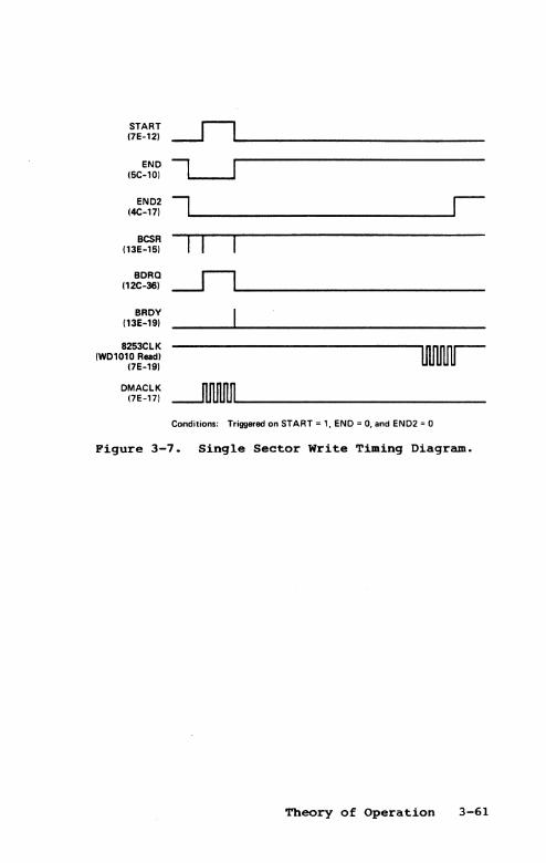
START ---11 17E-12)
END --, 15C-10)
EN02 --, 14C-17) ~ ________________ ~r-
BCSR I I I 113E-15)
BORQ ---11 112C-36)
BROY 113E-19)
8253CLK IW01010 Read)
17E-19)
OMACLK ---1lJlJll1J1 I7E-17)
Conditions: Triggered on START z 1, END = 0, and EN02 = 0
Figure 3-7. Single Sector Write Timing Diagram.
Theory of Operation 3-61
Clocks 0 and 1 are driven by DMACLK+ (DMA Clock) and its complement, which are generated from PAL 7E (pin 17). (See the "Programmable Array Logic" subsection in Section 2, "Archi tecture, " for programming information on PAL 7E.) When START+ becomes high, signifying a DMA request to the XBus master, 5C issues a low signal (pin 13), which is inverted at 4E (pin 3) and again at 4E (pin 9), generating XDRQ3- (X-Bus DMA Request, Priority 3) via connector J1, pin 58. (See the "State Sequencer" subsection, below, for the operation of 5C. ) Note that START+ from PAL 7E (pin 12) is generated to register 5B (pin 4), forcing a high output at pin 2 of 5B. This high signal loops back to pin 5 of 5B during the next 2MHZ+ transition at pin 9, generating a low signal at pin 6 that enables 4E (pin 19).
The X-Bus master responds with XDACK3- (X-Bus DMA Acknowledge, Priority 3) via connector Jl, pin 57, as shown in Figure 3-1, page 5. XDACK3- is inverted at 7F (pin 9) as ACK+ (Acknowledge). (See the "State Sequencer" subsection, below, for state information.) ACK+ is inverted at pin 5 of 4E and driven as AEN- (Address Enable). As shown in Figure 3-1, page 4, AEN- enables buffer 6F at pins 1 and 19, which generates XADR0- and XADRl1-through XADR17- to connector J1, pins 111 and 67 through 73. Note that address lines XADRllthrough XADR17- are controlled by data bits D0+ through D6+ at X-Bus Extended Address register 6E. See the "X-Bus Extended Address Register (Port XX0Eh)" in Section 2, "Architecture," for data bit functions.
Note that XBHE+ (X-Bus High Enable) is generated from buffer pin 11 of lC to connector Jl, pin 89 (Figure 3-1, page 5).
3-62 Floppy/Hard Disk Manual
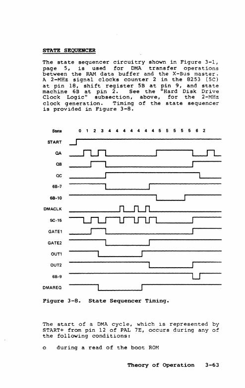
STATE SRQUDen
The state sequencer circuitry shown in Figure 3-1, page 5, is used for DMA transfer operations between the RAM data buffer and the X-Bus master. A 2-MHz signal clocks counter 2 in the 8253 (5C) at pin 18, shift register 5B at pin 9, and state machine 6B at pin 2. See the "Hard Disk Drive Clock Logic" subsection, above, for the 2-MHz clock generation. Timing of the state sequencer is provided in Figure 3-8.
State 012344444445555562
START ..J QA
QB __ ~r-I~ ________________ ~ QC
6B-7
6B-10
OMACLK
SC-15
GATE1 ____ ~r-I~ __________________ ~
GATE2
OUT1
OUT2
6B-9 u OMAREQ
Figure 3-8. State Sequencer Timing.
The start of a DMA cycle, which is represented by START+ from pin 12 of PAL 7E, occurs during any of the following conditions:
o during a read of the boot ROM
Theory of Operation 3-63
o after the WD1010 finishes a read operation from the hard disk
o before the WD1010 performs a write operation to the hard disk
The X-Bus master loads counter 0 of programmable interval timer SC with the total number of words that have to be transferred. Counter 1 specifies the number of transfers in one DMA burst, and counter 2 is used as a delay before another DMA transfer.
START+ initiates the DMA transfer at pin 4 of shift register SB. Note that the outputs of state machine 6B are all low at this time (that is, state 0). Therefore, a low signal is generated from pin 14 of 6B, enabling buffer lC at pin 10. An inactive DMACLK+, therefore, is inverted at 6D (pin 16), forcing a high signal at the counter 1 input of sc (pin 15).
On the next 2-MHz clock, a high signal is generated from pin 14 of 6B, disabling buffer lC at pin 10. A I-kilohm resistor (RP4) causes 6D to generate a low signal from pin 16.
During state 2, a high signal is again generated from 6D (pin 16), forcing pin 15 of SC high. In addition, a high signal is generated from pin 13 of 6B, which loads into gate 1 of SC at pin 14.
The purpose of states 1 and 2 described above is to set up the output for counter 1. At the start of state 3, SC generates a low pulse from pin 13 to pin 12 of SB, and to pin 17 of 4E. Inverter 4E, therefore, generates a high signal (pin 3), which inverts again at pin 9 of 4E. As a result, XDRQ3- is generated to the X-Bus master via connector Jl, pin 58.
In response, the X-Bus master generates XDACK3-back via connector Jl, pin 57. Then, DMACLK+ is generated during state 4 from 7E (pin 17), clocking SC at pin 15. After three words are read by the X-Bus master (signified by three DMACLK+ pulses as shown in Figure 3-8), the counter 1 output at pin 13 of SC becomes high.
Note from Figure 3-8 that QC of 6B becomes high at the start of state 4. This signal is NANDed at gate 8A with a high signal caused by the low
3-64 Floppy/Bard Disk Manual
signal output of counter 1 (pin 13 of SC). Therefore, a low siC!nal is generated from SA at pin 6, which inhibits 6B (pin 7) from counting.
After three DMACLK+ pul ses, the counter 1 output of sc (pin 13) becomes high, forcing the output of SA (pin 6) high and enabling 68 at pin 7, which initiates state 5.
At the start of state 5, the counter 2 output of SC at pin 17, which determines the timeout before another DMA transfer, becomes low and inhibits 6B from counting. (Note that the gate of counter 2 is controlled by the counter 1 output as shown in Figure 3-S.) After the specified timeout, a high signal is generated from sc at pin 17, enabling 6B at pin HI.
During state 6, a high signal is generated from pin 13 of 6B, which is NANDed with a high signal generating from 6B (pin 12) at gate SA, forcing a low signal from pin S that loads 6B (pin 9). The cycle then repeats itself beginning at state 2.
At the end of state 6, a low signal is generated from 6B (pin 12) that inverts at NAND gate SA (pin 6) enabling 6B at pin 7. In addition, this low signal disables gate 8A at pin S.
Theory of Operation 3-65
HARD DISK DRIVE READ/WRITE CIRCUITRY
READ
MPH Data
During a read, differential data from the selected hard disk drive (MFM13+ and MFM13-, or MFMl+ and MFMl-, connecting at connector Jl, pins 21' and 22, or 44 and 41, respectively) is driven to RS-422 receiver lIB at pins 15 and 14, or 9 and 113. (See Figure 3-1, page 4.)
Mul tiplexer llA determines from which drive the data is connecting via select lines Sl+ or S2+. When either Sl+ or S2+ is high at Hard Disk Drive Control register 3E (Figure 3-1, page 3), a high signal at pin 113 or 1 of llA (Figure 3-1, page 4) forces a low signal at pin 8, clocking pulse-width shaper flip-flop 12A at pin 11. Since pin 12 of l2A is connected to +5 V through I-kilohm resistor RP2, a high signal is generated from pin 9 through delay line l2B. After 413 nsec, a high signal is inverted at gate 7F (pin 18), to clear l2A at pin 13. This allows a 513-nsec pulse width signal at pin 9.
After 11313 nsec, a high signal generates to the WDl13113 (12C) at pin 37.
The 513-nsec pulse width from pin 9 of l2A triggers one-shot 13B at pin 4. The RC network consisting of R6 and Cl5 creates a 2313-nsec pulse width. A string of low bits (0's) or high bits (l's) constantly retriggers 13B, causing a high signal at pin 6 that informs 12C at pin 34 that a string of unchanging bits is generating from the selected hard disk drive.
When the string terminates, 13B times out and issues a low signal at pin 6 to notify 12C at pin 34 that the string has ceased.
When l2C detects a data string, it issues a high signal from pin 38 as RG+ (Read Gate). RG+ is inverted at pins 7 and 5 of l2E as RDGT+ (Read Gate), which generates to multiplexer llA (pin 5) and its complement, which generates to multiplexer llA (pin 3). When RG+ is asserted from 12C, therefore, llA is tied to MFM data generating from l2A (pin 9).
3-66 Floppy/Hard Disk Manual
Note that when 12C is not reading data from the selected hard disk drive (that is, the valid data string is not detected), RG+ is not asserted, and the phase-detection circuitry described below is locked to a reference by the 10-MHz reference clock. The reference clock generates from J-K flip-flop 10B at pin 5, as a result of the 20-MHz oscillator at 10A.
Phase-Detection Circuitry
PLLREF+ (Phase-Locked Loop Reference) is generated from llA (pin 6) to phase-detector enable flipflop 4B (pin 1) and phase-comparison flip-flop 3B (pin 1), which detect either the MFM data reference or the 10-MHz clock reference.
Since pin 3 of phase-detector enable flip-flop 4B is strapped to +5 V, a high signal is generated from pin 5 to set (enable) phase-comparison flipflops 3B and 4B at pins 3 and 11, respectively, and open a phase-comparison window. Flip-flops 3B and 4B should be clocked simultaneously. If an error exists between the frequency of the MFM data and voltage-controlled oscillator (Veo) output from IB (pin 7), one of the phase-comparison flipflops will be clocked before the other. For example, if the VCO is running too fast, a high signal from lB (pin 7) clocks 4B (pin 13) before 3B (pin 1) is clocked by MFM data. In this case, 4B will generate a high signal from pin 9, and 3B will generate a low signal from pin 5.
The high signal from 4B (pin 9) forces exclusive OR gate 4A (pin 8) low, which causes NAND gate 3A to output a high signal at pin 3. Simultaneously, the low signal from 3B (pin 5) forces exclusive OR gate 4A (pin 11) high. This high signal is NANDed at gate 3A with the high signal that was propagated by 4B (pin 9) to output a low signal at pin 11.
Since pins 4 and 11 inputs of phase-frequency detector 2A are active-low, the low signal from 3A (pin 11) causes 2A to pump down (pin 11). Therefore, a low signal is generated from pin 8 to oscillator IB (pin 2), causing the output frequency of lB (pin 7) to run slow.
When the signal is
MFM data generated
clocks 3B at pin I, a high from pin 5 to 2A at pin 1.
Theory of Operation 3-67
When both pins 3 and 1 of 2A become high, a low signal is genera ted from pin 6, which forces 3A (pin 8) low, resetting phase-detector enable flipflop 4B, and phase-comparison flip-flops 3B and 4B and, therefore, closing the phase-comparison window.
When IB is running slow, the MFM data will clock 3B at pin 1 before 4B (pin 13) is clocked by the output of IB (pin 7). Therefore, a high signal is generated from 3B at pin 5, forcing the input of 2A at pin 11 high to inhibit 2A from pumping down. In addition, the low signal from 4B at pin 9 forces the input of 2A at pin 4 low, enabling 2A to pump up.
In summary, when the phase is different at pins 1 and 3 of phase-frequency detector 2A (that is, between the reference voltage from pin 5 of 3B and the variable oscillator output from pin 9 of 4B), 2A pumps up or down to control the frequency of IB at pin 2. When pin 4 of 2A is low and pin 11 of 2A is high, the frequency increases at pin 8. When pin 11 of 2A is low and pin 4 of 2A is high, the frequency decreases at pin 8. When pin 2 of IB becomes high, the output frequency increases; when pin 2 becomes low, the output frequency decreases.
The output of lB at pin 7 clocks J-K flip-flop 3B at pin 13, to generate RDCLK+ (Read Clock) at pin 9. RDCLK+ connects to pin 39 of the WD1010 (12C). When a string of 0s or Is is detected, the phaselocked loop is clocked to MFM data, the RDCLK+ becomes high, and l2C anticipates a string of 0s or Is and searches the ID field. Then 12C starts loading the RAM data buffer.
Phase Synchronization
Shift-register 2B is used to start the phaselocked loop circuitry at the same phase as the incoming MFM data. MFM data, which is represented as PLLREF+, clocks 2B at pin 9. After four clock cycles, a low signal is generated from pin 14 and exclusive ORed at gate 4A with RDGT+ (pins 2 and 1, respectively). This C2'.tlses a high signal to genera te at pin 3, which is inverted at pin 4 of 9A, enabling lB (pin 6).
3-68 Floppy/Hard Disk Manual
Note that before RDGT+ is propagated through 2B, a high signal is generated from pin 14, causing gate 4A to produce a low signal that is inverted at pin 4 of 9A, disabling IB at pin 6.
WRITE
When the WDl~l~ (12C) writes data, it issues WD+ (Write Data) at pin 21 (Figure 3-1, page 4). The data is clocked by the l~-MHz clock generated from J-K flip-flop l~B at pin 6 as a result of 2~-MHz oscillator l~A. The MFM clock and data pulses are driven at 2F as WFM~+ and WFM~-, or WFMl+ and WFMl- to the selected hard disk drive (via connector Jl, pins 19 and 2~, or 39 and 4~).
Theory of Operation 3-69
8253 PROGRAMMABLE INTERVAL TIMERS
FLOPPY DISK OPERATION
If WD2797-02 formatter/controller 2C (shown in Figure 3-1, page 7) is prompted to perform a read operation on a nonexistent floppy disk sector, such as sector 17 on a l6-sector floppy disk, or if it is asked to read an entire track of data, 2C makes a futile search for the missing sector before issuing an interrupt request to the X-Bus master. Since this operation takes five revol utions of the floppy disk media (or about 1000 milliseconds), the 8253 programmable interval timer (4C) is used to terminate the read or write command after the last byte is read. This also gives 2C enough time to compute the two CRC bytes if a read error has occurred.
The total number of bytes to be transferred is loaded into 4C. When the read or write operation is complete, 4C interrupts the X-Bus master. The X-Bus master, in turn, issues a Force Interrupt command to 2C to terminate the search.
A functional block diagram of the interval timer logic i.s shown in Programming requirements for 4C are Section 2, "Architecture."
programmable Figure 3-9.
described in
The pin assignments and functions of 4C are provided in Table 3-4.
As shown in Figure 3-1, page 7, the 8253 programmable interval timer 4C is selected when 1-of-8 decoder IlF issues 8253CS- at pin 10, as described in the "Floppy/Hard Disk Module Device Decoding" subsection, above. When selected, the X-Bus master writes to several registers in 4C (using the XIOWR- strobe) to set the timing mode (always equal to 0, Interrupt on Terminal Count) and to specify the number of bytes in counter 0 to be transferred.
The X-Bus master can select one of several registers by using XADR1- and XADR2- X-Bus address lines, and can read from or write to the selected register by using the XDAT0- through XDAT7- lines. (See the "X-Bus Data Interface" subsection, above.) XADR1- is inverted at 7F (pin 14) before generating to the A0+ input of 4C (pin 19). XADR2- is inverted at. 7F (pin 12) before generating to the Al+ input of 4C (pin 20).
3-78 Floppy/Hard Disk Manual
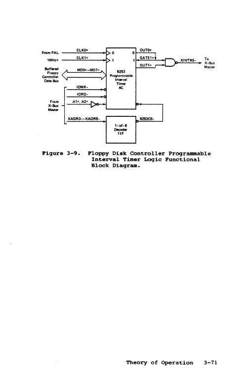
From PAL
lMHz+
Bufforod Floppy
Controllor Deta Bu,
From X-Bul -
CLKo.
CLK1+
~ MOo.-M07+ ..
'I- v
IOWR-
IORD-
{ A"~ ~ XADR3--XA:S-
0 0
1 1
8253 Programmable
IMOrYal Tim.
4C
1-ot-8 Dooodor
llF
OUTo.
GATE1+1
OUT1+
8253CS-
-~
I
XINTRS- To X-Bus Master
Pigure 3-9. Ploppy Disk Controller Programmable Interval Timer Logic PUDctional Block Diagram.
Theory of Operation 3-71
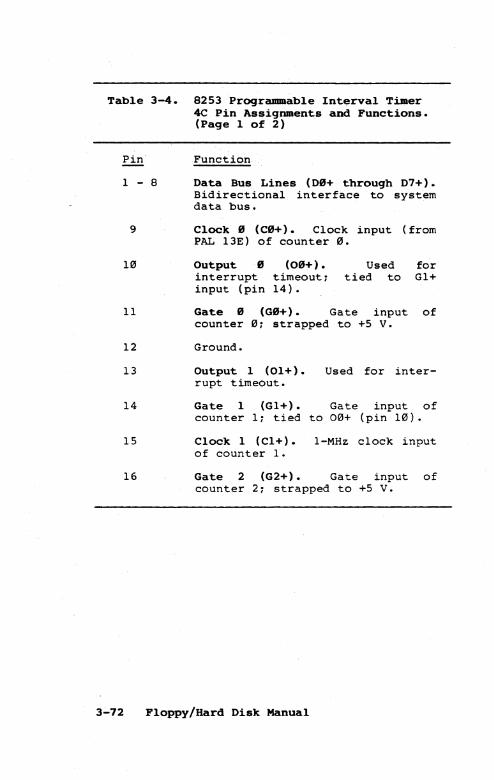
Table 3-4. 8253 Programmable Interval Timer 4C Pin Assignments and Functions. (Page 1 of 2)
~. Function
1 - 8 Data Bus Lines (D"+ through D7+). Bidirectional interface to system data bus.
9 Clock" (C,,+). Clock input (from PAL 13E) of counter ".
1"
11
12
13
14
15
16
3-72
Output " (00+). Used for interrupt timeout: tied to G1+ input (pin 14).
Gate "(G"+). Gate input of counter ": strapped to +5 V.
Ground.
Output 1 (01+). rupt timeout.
Used for inter-
Gate 1 (G1+). Gate input of counter 1: tied to 0"+ (pin 1").
Clock 1 (C1+). I-MHz clock input of counter 1.
Gate 2 (G2+). Gate input of counter 2: strapped to +5 V.
Floppy/Bard Disk Manual
Table 3-4. 8253 Programmable Interval Timer 4C Pin Assignments and Functions. (Page 2 of 2)
Pin Function
17 Output 2 (02+). Signal to PALs; used to tabulate the total number of words for internal use by 12C.
18
19, 20
21
22
23
24
Clock: 2 (C2+). Clock input from PAL used to reset counter 2.
Address Lines (AS+ and AI+). Used to select one of the three counters or the Control Word register for read or write operations; connected to X-Bus address lines XADRl- and XADR2-.
Chip Select (CS-). Enables 4C when llF issues 8253CS- from pin 10 as described in the "Floppy/Hard Disk Module Device Decoding" subsection.
Read (RD-) • Signifies r/o read operation.
Write (WR-) • Signifies r/o write operation.
Power (+5 V).
Theory of Operation 3-73
Read operations are indicated When XIORDgenerates through pin 3 of buffer l0F (Figure 3-1, page 2) to the RD- (Read) input of 4C (pin 22) shown in Figure 3-1, page 7. Similarly, write operations are indicated when XIOWR- generates through pin 5 of 10F to the WR- (Write) input of 4C at pin 23. Internal registers of 4C are listed below with their addresses in the module relative to the module base I/O address (XXh):
Read Register Write Register A2+ hl:t (RD-) (WR-)
0 0 Read counter 0 Load counter 0 (XX10h) (XX10h)
0 1 Read counter 1 Load counter 1 (XX12h) (XX12h)
1 0 Read counter 2 Load counter 2 (XX14h) (XX14h)
1 1 Mode word (XX16h)
Counters 0 and 1 are used for the interrupt function. Counter 0 is loaded with the total byte count of the read operation. Counter 1 is loaded with a fixed time interval to time out (about 40 microseconds), which allows 2C to compute the two CRC bytes at the last sector of the transfer if a read error has occurred. If counter 1 is not used, a race condition can occur if the X-Bus master issues a Force Interrupt command to 2C before it actually finishes with the CRC bytes. Therefore, both counters time out before an interrupt is sent to the X-Bus master.
When counter 0 times out, its output becomes high at pin 10 and generates to enable gate 1 at pin 14. Then, counter 1 outputs a high signal at pin 13. The high signals from both counters are generated to NAND gate IE (pins 5 and 4, respectively) to assert XINTR5- to the X-Bus master via connector Jl, pin 114.
Counter 0 is clocked by DM+ (DMA), once for every byte transferred by 2C, at pin 9 of 4C, indicating that the Data register in 2C is being accessed. Counter 1 is clocked at pin 15 by the I-MHz output at pin 5 of divide-by-two flip-flop 9B shown in Figure 3-1, page 4.
3-74 Floppy/Hard Disk Manual
Note that counter 2 is not used by the floppy controller: counter 2C is used by the hard disk controller, as described below in the "Hard Disk operation" subsection.
HARD DISK OPERATION
The hard disk controller l2C uses both 8253 programmable interval timers resident to the Floppy/Hard Disk Module (that is, 4C and 5C). Counter 2 of 4C is used to tabulate the total number of words for internal use by l2C (since 12C does not support multiple-sector transfers). All counters of 5C are used for DMA transfers.
A functional block diagram of the programmable interval timer logic used by the hard disk controller is shown in Figure 3-10. Programming requirements for 4C and 5C are described in Section 2, "Architecture." In addition, timing diagrams are provided in Figures 3-5 through 3-7.
The pin assignments and functions of 4C are provided in Table 3-4. The pin assignments and functions of 5C are provided in Table 3-5.
As shown in Figure 3-1, page 7, 5C is selected when 1-of-8 decoder IlF (Figure 3-1, page 7) issues W8253EN- (pin 10) as described in the "Floppy/Hard Disk Module Device Decoding" subsection, above. When selected, the X-Bus master writes to several registers in 5C (using the XIOWR- strobe ~hown in Figure 3-1, page 2) to set the timing mode.
As shown in Figure 3-1, page 2, the X-Bus master can select one of several registers by using XADR1- and XADR2- X-Bus address lines, and can read from or write to the selected register. (See "X-Bus Data Interface," above.) XADR1- is inverted at 7F (pin 14) before generating to 5C as Al+. XADR2- is inverted at 7F (pin 12) before generating to 4C as A2+. As shown in Figure 3-1, page 5, Al+ connects to the A0+ input of 5C (pin 19), and A2+ connects to the Al+ input of 5C (pin 20) •
Theory of Operation 3-75
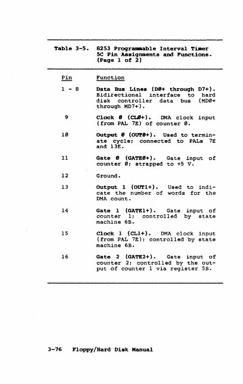
Table 3-5. 8253 Programmable Interval Timer 5C Pin Assignments and Functions. (Page I of 2)
Pin Function
1 - 8
9
10
11
12
13
14
Data Bus Lines (D9+ through Bidirectional interface to disk controller data bus through MD7+).
D7+) • hard
(MD0+
Clock 9 (CLS+). DMA clock input (from PAL 7E) of counter 0.
OUtput 8 (OUT9+). Used to terminate cycle; connected to PALs 7E and l3E.
Gate 8 (GATE8+). Gate input of counter 0; strapped to +5 v.
Ground.
Output I (OUT1+). Used to indicate the number of words for the DMA count.
Gate I (GATE1+). Gate counter 1; controlled machine 6B.
input of by state
15 Clock 1 (CL1+). DMA clock input (from PAL 7E); controlled by state machine 6B.
16 Gate 2 (GATE2+). Gate input of counter 2; controlled by the output of counter 1 via register 5B.
3-76 Floppy/Bard Disk Manual
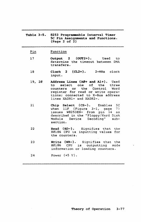
Table 3-5. 8253 Programmable Interval Timer 5C Pin Assignments and Functions. (Page 2 of 2)
~ Function
17 Output 2 (OUT2+). Used to determine the timeout between DMA transfers.
18
19, 29
21
22
23
24
Clock 2 (CL2+). input.
2-MHz clock
Address Lines (A8+ and Al+). Used to select one of the three counters or the Control Word register for read or write operationsr connected to X-Bus address lines XADR1- and XADR2-.
Chip Select (CS-). Enables 5C when llF (Figure 3-1, page 7) issues W8253EN- from pin 14 as described in the "Floppy/Hard Disk Module Device Decoding" sub-section.
Read (RD-). Signifies that the 80186 CPU is inputting values for the counters.
Write (WR-). Signifies that the 80186 CPU is outputting mode information or loading counters.
Power (+5 V).
Theory of Operation 3-77
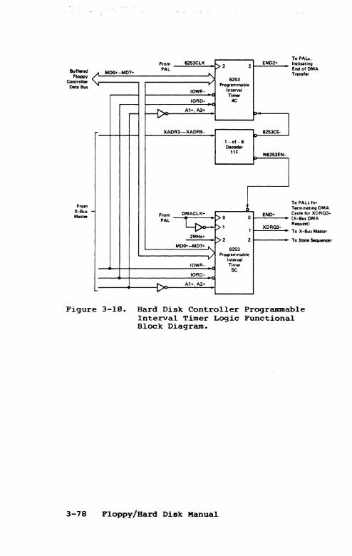
Bu .... od Floppy
Controller Data Bus
From X-Bus Master
<-. MOO+-MD7+
r---
C-
F,om 8253CLK PAL
IOWR-
IORD-
~ A1+, A2+
XADR3--XADR5-
From OMACLK+
PAL
1 " V
2MHz+
MOO+-MD7+ "-
.. IOWA-
IORO-
" A1+, A2+
2 2
8253 Programmable
Interval Timer
4C
1 -of - 8 Docode,
l1F
1 0 0
1 1
2 2
8253 Programmable
Interval Timer
5C
EN02+
8253CS-
W8253EN-
ENO+
XDRQ3-
To PALs, Indicating End of DMA Transfer
To PALs for Terminating OMA Cvcle for XORQ3-IX-BusOMA Request}
To X-Bus Master
To State Sequencer
Figure 3-le. Hard Disk Controller Programmable Interval Timer Logic Functional Block Diagram.
3-78 Floppy/Hard Disk Manual
':, \ .... :.
Read operations are indicated when XIORDgenerates through pin 3 of buffer leF (Figure 3-1, page 2) to the RD- (Read) input of 5C (pin 22) shown in Figure 3-1, page 5. Similarly, write operations are indicated when XIOWR- generates through pin 5 of UF to the WR- (Write) input of 5C at pin 23.
Internal registers of 5C are listed below with their addresses in the module relative to the module base I/O address (XXh):
Read Register Write Register A2+ Al+ (RD-) (WR-)
111 111 Read counter 111 Load counter e (XX3eh) (XX3eh)
111 1 Read counter 1 Load counter 1 (XX32h) (XX32h)
1 111 Read counter 2 Load counter 2 (XX34h) (XX34h)
1 1 Mode word (XX36h)
When the X-Bus master loads a command in con-troller l2C, the following times are set in counters 111, 1, and 2 of 8253 5C:
o word count (counter 111)
o DMA burst count (counter 1)
o DMA delay count (counter 2)
In addition, counter 2 of 8253 4C shown in Figure 3-1, page 7, is set to provide internal timing for l2C.
After the mode control is loaded, END+ and END2+ become low. Then, l2C accesses the ID field, reads the content from the hard disk, and loads the content into the RAM data buffer. During this time, the inactive END2+ counts. At the end of the count, END2+ becomes high, signifying that l.2C has written data into the RAM data buffer. PAL 7E then resets counter 2 of 4C (pin 18) by issuing 8253CLK- from pin 19. 7E then generates a START+ signal from pin 12 to allow the DMA transfer.
Theory of Operation 3-79
Refer to the "State Sequencer" subsection, above, for state information.
POWER SUPPLIES
Two standard dc/ dc power converters are used in the Floppy/Hard Disk Module. One supplies +12 Vdc for the drives while the other supplies +5 Vdc for the drives and controller circuitry. For more information, refer to the ~ System Manual.
3-8111 Floppy/Hard Disk Manual
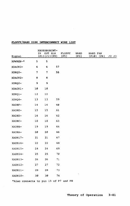
FLOPPY /HARD DISK INTERCONNECT WIRE LIST
XBUSXBUSCNT-IN OUT RLR FLOPPY HARD HARD FAN
Sisnal (PI) (J1) (P9) (P5 ) (P3) (PHl) (P6) J2 J3
XPWREN-" 5 5
XDACK3- 6 6 57
XDRQ3- 7 7 58
XDACK2- 8 8
XDRQ2- 9 9
XDACK1- 10 10
XDRQ1- 12 12
XDRQ4- 13 13 59
XADRF- 14 14 60
XADRE- 15 15 61
XADRD- 16 16 62
XADRC- 18 18 63
XADRB- 19 19 64
XADRA- 20 20 66
XADR17- 21 21 67
XADR16- 22 22 68
XADRI5- 24 24 69
XADR14- 25 25 70
XADRI3- 26 26 71
XADR12- 27 27 72
XADRll- 28 28 73
XADR10- 30 30 74
"Also connects to pin 15 of P7 and P8
Theory of Operation 3-81
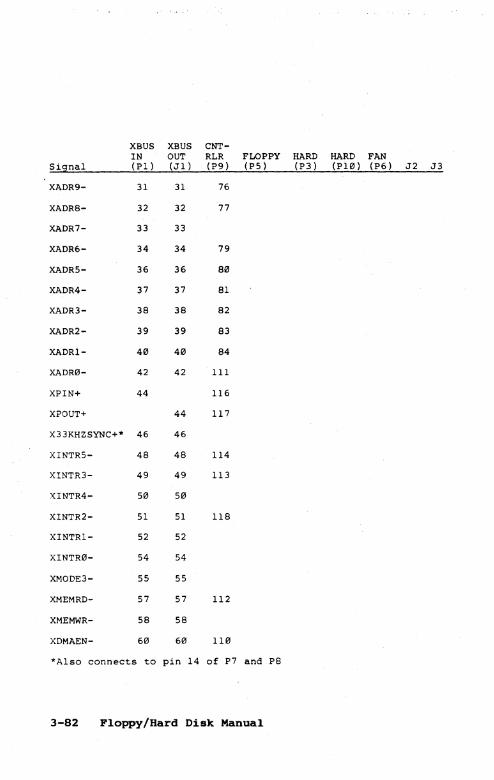
XBUS XBUS CNT-IN OUT RLR FLOPPY HARD HARD FAN
SiSlnal (PI) (Jl) (P9) (P5) (P3) (PI0) (P6) J2 J3
XADR9- 31 31 76
XADR8- 32 32 77
XADR7- 33 33
XADR6- 34 34 79
XADR5- 36 36 80
XADR4- 37 37 81
XADR3- 38 38 82
XADR2- 39 39 83
XADRl- 40 40 84
XADR0- 42 42 III
XPIN+ 44 116
XPOUT+ 44 117
X33KHZSYNC+* 46 46
XINTR5- 48 48 114
XINTR3- 49 49 113
XINTR4- 50 50
XINTR2- 51 51 118
XINTR1- 52 52
XINTR0- 54 54
XMODE3- 55 55
XMEMRD- 57 57 112
XMEMWR- 58 58
XDMAEN- 60 60 110
*A1so connects to pin 14 of P7 and P8
3-82 Floppy/Hard Disk Manual
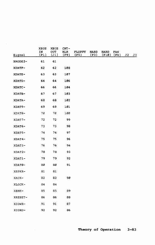
XBUS XBUS CNT-IN OUT RLR FLOPPY HARD HARD FAN
Signal (PI) (JI) (P9) (PS) (P3) (PH' ) (P6) J2 J3
XMODE2- 61 61
XDATF- 62 62 108
XDATE- 63 63 107
XDATD- 64 64 106
XDATC- 66 66 104
XDATB- 67 67 103
XDATA- 68 68 102
XDAT9- 69 69 101
XDAT8- 70 70 100
XDAT7- 72 72 99
XDAT6- 73 73 98
XDATS- 74 74 97
XDAT4- 75 75 96
XDAT3- 76 76 94
XDAT2- 78 78 93
XDAT1- 79 79 92
XDAT0- 80 80 91
XSPKR- 81 81
XACK- 82 82 90
XLOCK- 84 84
XBHE- 85 85 89
XRESET- 86 86 88
XIOWR- 91 91 87
XIORD- 92 92 86
Theory of Operation 3-83
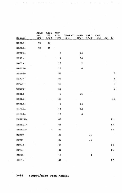
XBUS XBUS CNT-IN OUT RLR FLOPPY HARD HARD FAN
Sisnal (PI) (Jl ) (P9) (P5) (P3) (PI0) (P6) J2 J3
XPCLK+ 93 93
XDCLK- 95 95
STEPl- 6 24
DIRl- 4 34
RWCl- 18 2
WRGTl- 13 6
STEP2- 51 5
DIR2- 52 6
RWC2- 49 7
WRGT2- 50 8
DSEL£I- 3 26
DSELl- 47 10
HSEL£I- 9 14
HSELl- 10 18
HSEL2- 16 4
EHSEL0- 48 11
EHSELl- 46 12
EHSEL2- 43 13
MFM£!+ 21 17
MFM£!- 22 18
MFMl+ 44 14
MFM1- 41 16
SEL£!- 17 1
SE.Ll- 42 17
3-84 Floppy/Bard Disk Manual
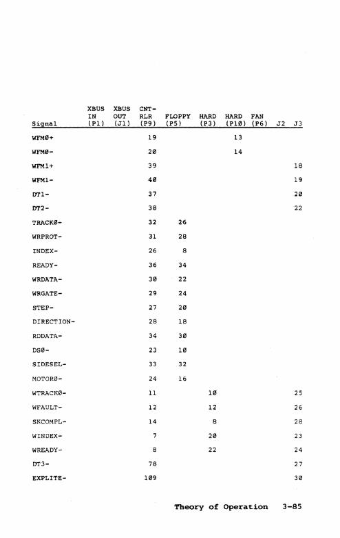
XBUS XBUS CNT-IN OUT RLR FLOPPY HARD HARD FAN
Sisnal (PI) (Jl) (P9) (PS) (P3) (PI0) (P6) J2 J3
WFM0+ 19 13
WFM0- 20 14
WFMl+ 39 18
WFMl- 40 19
DTl- 37 20
DT2- 38 22
TRACK0- 32 26
WRPROT- 31 28
INDEX- 26 8
READY- 36 34
WRDATA- 30 22
WRGATE- 29 24
STEP- 27 2121
DIRECTION- 28 18
RDDATA- 34 3121
DS0- 23 10
SIDESEL- 33 32
MOTOR0- 24 16
WTRACK0- 11 10 25
WFAULT- 12 12 26
SKCOMPL- 14 8 28
WINDEX- 7 20 23
WREADY- 8 22 24
DT3- 78 27
EXPLITE- 11219 30
Theory of Operation 3-85
HARD DISK EXPANSION
3-86
A Hard Disk Expansion Module can be connected to the right side of the Floppy/Hard Disk Module (looking from the front). See the Installation Guide for details.
A hard disk expansion interconnect wire list is provided below.
Floppy/Bard Disk Manual
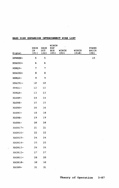
HARD DISK EXPANSION D1'l'ERCONNBCT WIRE LIST
WINCH XBUS XBUS EXP POWER IN OUT BUS WINCH WINCH BRICK
Signal (Pl) (.12 ) (P5) (P3) (P1") (P8)
XPWREN- 5 5 15
XDACK3- 6 6
XDR03- 7 7
XDACK2- 8 8
XDR02- 9 9
XDACKl- 1" 1"
XDRQl- 12 12
XDRQ4- 13 13
XADRF- 14 14
XADRE- 15 15
XADRD- 16 16
XADRC- 18 18
XADRB- 19 19
XADRA- 2" 2"
XADRI7- 21 21
XADRI6- 22 22
XADR15- 24 24
XADR14- 25 25
XADRI3- 26 26
XADR12- 27 27
XADRll- 28 28
XADR1"- 3" 30
XADR9- 31 31
Theory of Operation 3-87
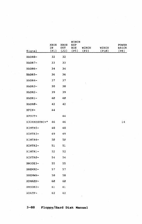
WINCH XBUS XBUS EXP POWER IN OUT BUS WINCH WINCH BRICK
Sisnal (PI) (J2) (P5) (P3) (PI13) (P8)
XADR8- 32 32
XADR7- 33 33
XADR6- 34 34
XADR5- 36 36
XADR4- 37 37
XADR3- 38 38
XADR2- 39 39
XADRl- 413 413
XADR13- 42 42
XPIN+ 44
XPOUT+ 44
X33KHZSYNC+* 46 46 14
XINTR5- 48 48
XINTR3- 49 49
XINTR4- 513 50
XINTR2- 51 51
XINTR1- 52 52
XINTR13- 54 54
XMODE3- 55 55
XMEMRD- 57 57
XMEMWR- 58 58
XDMAEN- 613 613
XMODE2- 61 61
XDATF- 62 62
3-88 Floppy/Bard Disk Manual
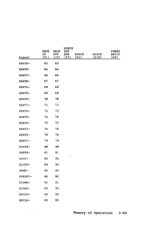
WINCH XBUS XBUS EXP POWER IN OUT BUS WINCH WINCH BRICK
Signal (Pi) (J2) (P5) (P3) (PHl) (P8 )
XDATE- 63 63
XDATD- 64 64
XDATC- 66 66
XDATB- 67 67
XDATA- 68 68
XDAT9- 69 69
XDAT8- 70 70
XDAT7- 72 72
XDAT6- 73 73
XDAT5- 74 74
XDAT4- 75 75
XDAT3- 76 76
XDAT2- 78 78
XDATi- 79 79
XDAT0- 80 80
XSPKR- 81 81
XACK- 82 82
XLOCK- 84 84
XBHE- 85 85
XRESET- 86 86
XIOWR- 91 91
XIORD- 92 92
XPCLK+ 93 93
XDCLK- 95 95
Theory of Operation 3-89
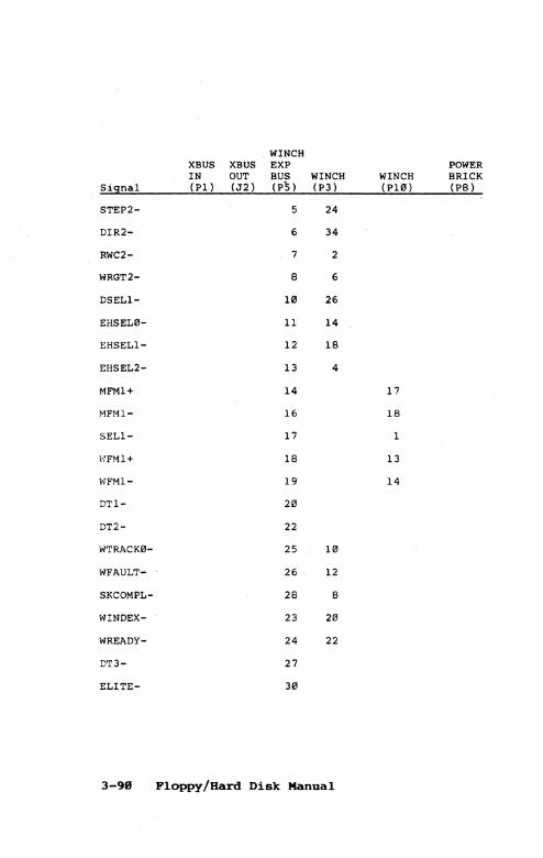
WINCH XBUS XBUS EXP POWER IN OUT BUS WINCH WINCH BRICK
Signal (Pl) (J2) (PS) (P3) (P10) (P8)
STEP2- 5 24
DIR2- 6 34
RWC2- 7 2
WRGT2- 8 6
DSEL1- 10 26
EHSEL0- 11 14
EHSEL1- 12 18
EHSEL2- 13 4
MFM1+ 14 17
MFM1- 16 18
SEL1- 17 1
"IFM1+ 18 13
WFM1- 19 14
DT1- 20
DT2- 22
WTRACK0- 25 HI
WFAULT- 26 12
SKCOMPL- 28 8
WINDEX- 23 2'"
WREADY- 24 22
DT3- 27
ELITE- 30
3-98 P1oppy/Hard Disk Manua1
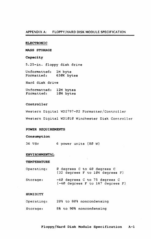
APPENDIX A: FLOPPY/HARD DISK MODULE SPECIFICATION
ELECTRONIC
MASS STORAGE
Capacity
5.25-in. floppy disk drive
Unformatted: 1M byte Formatted: 630K bytes
Hard disk drive
Unformatted: 12M bytes Formatted: 10M bytes
Controller
Western Digital WD2797-02 Formatter/Controller
Western Digital WD1010 Winchester Disk Controller
POWER REQUIREMENTS
Consumption
36 Vdc
ENVIRONMENTAL
TEMPERATURE
Operating:
Storage:
HUMIDITY
Operating:
Storage:
6 power units (80 W)
o degrees C to 40 degrees C (32 degrees F to 104 degrees F)
-40 degrees C to 75 degrees C (-40 degrees F to 167 degrees F)
20% to 80% noncondensing
8% to 90% noncondensing
Floppy/Hard Disk Module Specification A-I

APPENDIX B: MITSUBISHI MINI FLEXIBLE-DISK DRIVE - M4852/M4853-SPECI FICA TlONS
Mitsubishi M4B52/M4B53 B-1
MITSUBISHI MINI
IIIIIJ
FLEXIBLE-DISK DRIVE M4852/ M4853 (~.:~BHEIGHT)
; "[~\:J;;t~'; :~~~~-,1 t7}~.N .~ i: ~")~';::*~~;j~~ ........ t.".: . .' . .. .. _ ~:., I- •
Specifications
. , ' .:A': , ~
,'01 '. .' • • , ."
J..MITSUBISHI ELECTRIC CORPORATION
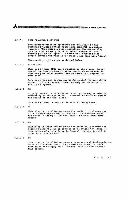
3.1.3
3.1.3.1
USER CHANGEABLE OPTIONS
Non-standard modes of operation are available to the customer by using option plugs, and some PC3 cut and/or jumpers. When using a plug, installing the option plug on a pair of square pins is a "short" condition, and removing it is an "open". A trace or a soldered wire jumper between two pads is a "short", and none is a "open".
The specific options are explained below.
050 TO 053
When two or more FOOs are connected to the system, jumper one of the four choices to allow the drive to be enabled when the particular select line is taken to a logical "0" condition.
Only one drive per system may be designated for each drive number. In other words, there can only be one drive "0", etc., in a system.
3.1.3.2 MX
If only one FOO is in a system, this option may be used to constantly select the drive. It causes to drive to ignore the status of the "OS" lines.
This jumper must be removed in multi-drive systems.
3.1. 3.2 HS
This plug is installed to cause the heads to load when the drive is selected by 050 through 053. This occurs after the drive is "ready". 00 not install HM or He with this option.
3.1.3.3 HM
This plug is installed to cause the heads to load when the motor on line (Pl-16) is brought to a logical "0" level. This occurs after the drive is "ready". 00 not install HS or HC with this option.
3.1. 3.4 HC
This plug is installed to cause a constant head load condition which occurs after the drive is ready to allow for proper seating of the floppy disk. 00 not install HS or HM with this option.
REV 7/13/83
3.1.3.5 MM
This plug is installed to cause the spindle motor to turn on and rotate the disk with the input of a logical "0" on the motor on line, Pl-16.
3.1.3.6 MS
This plug is installed to cause the spindle motor to turn on and rotate the disk when the drive is selected by applying a logical "0" on one of the drive select lines, 050 through 053.
3.1.3.7 H-l
Installing the "H" jumper in position 1 routes. whatever type of ·ready·signal is selected to be outputed from the drive to the head load circuit ready qualification input. .
3.1. 3.8 8-2
Installing the "H" jumper in position 2 routes the "current status· ready signal to the head load circuit ready qualification input.
3.1.3.9 8-3
Installing the "8" Jumper in position 3 routes the "held status" ready signal to the head load circuit ready qualification input.
3.1.3.10 R-2
Installing the "R" jumper in position status" ready output from the drive. a logical "0" when the floppy disk is speed.
3.1.3.11 R-3
2 enables a "current The output goes to rotating at proper
Installing the "R" jumper in position 3 enables a "held status· ready output from the drive. The output will be a logical "0' when a disk is inserted and correctly clamped in the drive. (Index pulses were detected correctly).
3.1.3.12 R-4
This option must not be used at this time.
REV 7/13/93
.J..IUlUJlIIII •• , ...... 1111 •• 1 .... iIi J
3.1.3.13 MC
Cutting this PCB trace causes the spindle motor to run whenever a floppy disk is inserted in the drive.
3.1.3.14 RD-RS
This option is associated with "R-4", and therefore has no significance at this time.
3.1.3.15 DI
Cutting this PCB trace disables the in-use input to the drive (Pl-4). This means that the only time the front panel LED will be lit will be when the drive is selected. The MX option cannot be used in conjunction with this modification; the in use LED will never be illuminated if it is.
3.1.3.16 WRITE PROTECT INVERSION
The option pads between IC's M1 and L1 are used to invert the logic of the write protect slot on the floppy disk. The trace from the center pad to the in-board pad must be cut, and the center pad must be jumped to the out-board pad to enable this option.
3.1.3.17 INPUT TERMINATIONS
All seven input lines to the drive are terminated (See section 3.1.1). The jumper plug located between IC's C5 and D5 should be removed on drives in multi-drive systems. with the exception of the drive the furthest electrical distance from the controller.
REV 7/13/83
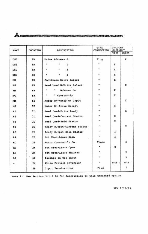
TYPE FACTORY NAME LOCATION DESCRIPTION CONNECTION SHIPM NT
Open Short
DSO 6B Drive Address 0 Plug X
DSl 6B · · 1 · X
DS2 6B · · 2 · X
DS3 6B · · 3 · X
MX 6B Continues Drive Select · X
HS 6B Head Load W/Drive Select " X
8M 6B · n W/Motor On " X
HC 6B · . Constantly · X
MM 5E Motor On-Motor On Input · X
MS 5E Motor On-Drive Select · X
HI 2L Head Load-Drive Ready " X
H2 2L Head Load-Current Status · X
H3 2L Head Load-Held Status " X
R2 2L Ready Output-Current Status " X
R3 2L Ready Output-Held Status " X
R4 2L Not Used-Leave Open " X
MC 2E Motor Constantly On Trace X
RD 21< Not Used-Leave Open · X
as 21< Not Used-Leave Shorted · X
DI 6B Disable In Use Input " X
- 2M Write Protect Inversion · Note 1 Note I
6B Input Terminations Plug 7
Note 1: See Section 3.1.3.16 for description of this unmarked option.
REV 7/13/83
4.7 DISK INSERTION
The .equence of events ~~at Occur with disk insertion are.
1) The user inserts the disk into the drive until an audible ·click· is heard. This indicates that the drive ejection mechanism has received the disk.
2) When the disk is fully inserted into the drive a meChanical switch is accuated, and the spindle motor starts to rotate.
3) The user clamps the disk on to the rotating spindle using the bridge handle. The handle is moved until an audible click is heard.
4) The disk starts to rotate, and the index sensor begins to detect pulses of light from the index LED.
5) Two index pulses are detected in a minimum period of time, Which switches the "current ready" and "held ready" logic to a true state. If the disk is not properly seated, this will not occur because the index hOIe in the disk will never allow light to strike the presise location required to activate the photo-transistor that is the index pulse sensor. The spindle motor is turned off.
6) Option jumper H-3 (or in some cases H-l) may be used to load the head on to the disk at this time. This is desirable if the user wishes to eliminate the head load and settling times associated with motor start/stop operation.
4.8 DISK REMOVAL
To remove the disk from the drive the user depresses the front panel door flop, which releases the bridge handle. The ejector mechanism then transports the disk out of the drive into the users fingers.
This action also resets the "held ready" status to a false condition, which can be detected by having the system controller poll the drive for its status (if the R-3 option is used) .
REV 7/13/83
CONTENTS
Page
CHAPTER I INTRODUCTION • • • • • • • • • • • • • • • • • • • • • • • • • .. .. • • • • • • • • • • • 1-
1.1 General Description............................................... 1-1.2 Specifications. . • • • • • .. • • • . • .. • • • • • • • • .. • . • • • .. • • • • • • • • • .. .. • .. • . 1-
1.2.1 Performance specifications •.•••••••••..••••••.••.•••. 1-1.2.2 Functional specifications .. .......................... 1-1.2.3 Physical specifications .. .................. .......... 1-1.2.4 Reliability specifications .. ......................... 1-
CHAPTER 2 OPERATION OF MAJOR COMPONENTS .......... .......... 2-
2.1 2.2 2.3 2.4 2.S
System Operation ............................................... . Electronic Circuits ............................................... . Rotation Mechanism ............................................. . Positioning Mechanism ..•.•••••.•.••••••••••••••••••••.••..••••.•. Read/Write Heads ............................................... .
- 1 - 1 - 3 - 3 - 3
CHAPTER 3 ELECTRICAL INTERFACE ............................... 3-
3.1
3.2
Signal Interface ................................................. . 3.1.1 Cabl1ng method and input line termination ••.••.•••..• 3.1. 2 3.1.3
3.1.4
Line driver and line receiver •••••••••••••••••••••••• Jumpers ........................................................................................ .. (1) MX ............................................. .
(2) OSO to OS3 .................................... .. (3) HS and HM ..................................... .. Input Slgnal lines •••.•••••.••••••••••••••••.••••.••• (1) Drive select 0 to drive select 3 .............. 0 .... ow ....... ..
(2) Side one select ................................ . (3) Direction select .............................................................. .. (4) Step ......••••••••.•••••••.•.••••••••.••••.••••. (5) Write gate ..................................... . /6) Write data ..................................... . (7) In use ......................................... . (8) Motor on •••••....•••.•...•••.•..••••.•••.•..••.•
3 -3 -3 - 4 3 -3 -3 - 5 3 - 5 3 -3 -3 - 6 3 - 7 3 -3 -3 -
- 8 3 -
3.1. 5 Output 5 ignal lines .. . . .. ....... .. .. .... .. • .. .. ... .. . .. .. .. ...... .. • . . . . .. . 3-(1) Index ........................................... 3-12 j Track 00 ....................................... . (3) Ready .......................................... . 14 j Ready data •••••.•••••••••••.•••••••...••.••••••. (5) Write protect ......................................... .
Power Interface .••...••.......•.••••...•..••....•........••..... 3.2.1 DC pcwer ............................................ .
- i -
3 -3 -3 -3 -3 -10
-10
P4ge
CHAPTER 4 FUNCTIONAL OPERATION •••••••••••••••••••••••••••••• 4-
4.1 Power On Sequencing............................. ••••• ....... •••• 4 - 1 4.2 Drive Selection • • • • • • • • • • • • • • • • • • • • • • • • • • • • • • • • • • • • • • • • • • • • • • • • • • • 4 '- 1 4.3 Positioning Operation. • • • • • • • • • • • • • • • • • • • • • • • • • • • • • • • • • • • • • • • • • • • • • 4 - 1 4.4 Side One Selection. •• •• •• •• • • •• • •• • • • • • • • •• •• •• • • • • •• • ••• •••• • • •• • 4 - 1 4.5 Read Operation .................................................. 4 - 2 4.6 Write Operation .......... , ••• •• •• • • • • • • .. ••• • • • • •• • •••• •• ••••••• • 4 - 2
CHAPTER 5 PHYSICAL INTERFACE. • • • • .. • • • • • • • • • • • • • • • • • • • • • • • • • • • 5 - 1
5.1 Silnal Connectors. • • • • • • • • • • • • • • • • • • • • • • • • • • • • • • • • • • • • • • • • • • • • • • • • 5 - 1 5.2 DC Power Connector (Jl/Pl) •••••••••••••••••••••••••••••••••••••••• 5 - 3 5.3 Fume Ground Connector (J5/P5) .................................... 5 - 3 5.4 Interface Connector Physical Location.. • • • • • • • • • • • • • • • • • • • • • • • • • • • • .. • 5 - 4
CHAPTER 6 DRIVE PHYSICAL SPECIFICATIONS........ •••• ........... 6 - 1
6.1 InstaUa tion Direction. ... • • • • • • • • • • • • • • • • • • • • • .. • • • • • • • • • • • • • • • • • • • • 6 - 1 6.2 Dimensions of M485 1 •.. . . . . . • . . • • . • • • • . • • . . . • • . • . • . . . . • • • • • • .. .. • 6 - 1 6.3 Dimensions ofM4853 ............................................. 6 - 1
CHAPTER 7 ERROR DETECTION AND CORRECTION •••••••••••••••••••• 7 - 1
7.1 Write Erron ..................................................... 7 - 1 7.2 Read Erron •••••••••.••••••••••••••••••••••••••••••••••••••••••• 7 - 1
CHAPTER 8 RESHIPMENT PRECAUTIONS. • • • • • • • • • • • • • • • • • .. • • • • • • • • •• 8 - 1
- ii -
~/IIIPPPPPPPI!IIPPPPPI!IIP/IIIPPPPPPPP/IIIPPPPPPI!IIPP/IIIPI!IIPPPP/IP/I/lPI!IIPPP/lIIPP, MITSUBISHI ELECTRIC
CHAPTER 1 INTRODUCTION
The Mitsubishi M4852/M4853 Flexible Disk Drives are high-performance, double-side, double bit and double track density flexible disk drive uSlng • standard S.2S-inch diskette, that provides maximum customer satisfaction even to those who demand high reliability and long service life.
- Main Features -
o Model M4852 is the standard size. and Model M4853 is half as high (41 IIJD) as the standard size.
o MOdel M4853 includes a diskette ejector for easy diskette removal.
o A new circular gimbal sprinq in the read/write head suspension mechanism greatly improves medium tracking performance.
o The steel band drive system for p)sitioning aChieves the best intertrack access time in its class: just 3 ms.
o The maintenance-free, DC, brushless, direct-drive motor obviates the bel t replacement necessary for convent iona1 counter par ts.
o Stable media interchangeability, wide off-track. window time margln, and excellent performance are maintained over wide ambient temperature and relative humidity ranges.
o The high-torque spindle motor permits control by aWl tching on and of f either the motor (starting time 250 ms) or the head load magnet (loading time less than 50 ms).
I .I General Oescription
o The M4853 Flexible Disk Drive is a twin-head, double-sided magnetic disk drive with a formatted memory cap~city of more than 635 kilobytes for double-density recordings.
o The M4853 reads and writes 5.25-inch, double-sided diskettes in double-density format.
a The M4853 employs the unique Mitsubishi circular gimbal spring for hol.:Hng and loading the magnetic heads to assure soft, steady contact with the medium. This means excellent read/write operation and a long service life for the medium. One of the outstanding features of this mechanism is reduction of the effect:; of jacket deformation and thickness variations, thereby stabillzing read/write performance and dispensing with the need for selecting products of a spec i f ic manufacturer.
1 - 1
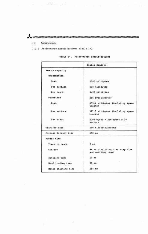
1.2 Spel'ificatiun!ot
1. 2~ 1 Performance specifications (Table 1-1)
Table 1-1 Performance Specifications
Double Densi ty
Memory capacity
Unformatted
Disk 1000 kilobytes
Per surface 500 kilobytes
Per track 6.25 kilobytes
Formatted 256 bytes/sector
Disk 655.4 kilobytes (including apare tracks)
Per surface 327.7 kilobytes (including spare tracks)
Per track 4096 bytes • 256 bytes x 16 sectors
Transfer rate 250 kilobits/second
Average latency time , 100 ms
Access time
Track to tt;ack i
3 rns
Average 94 ms (including 3 ms step time I and settling time) ,
Settling time i 15 rns
Head loading time I 50 rnS
Motor starting time i 250 liS
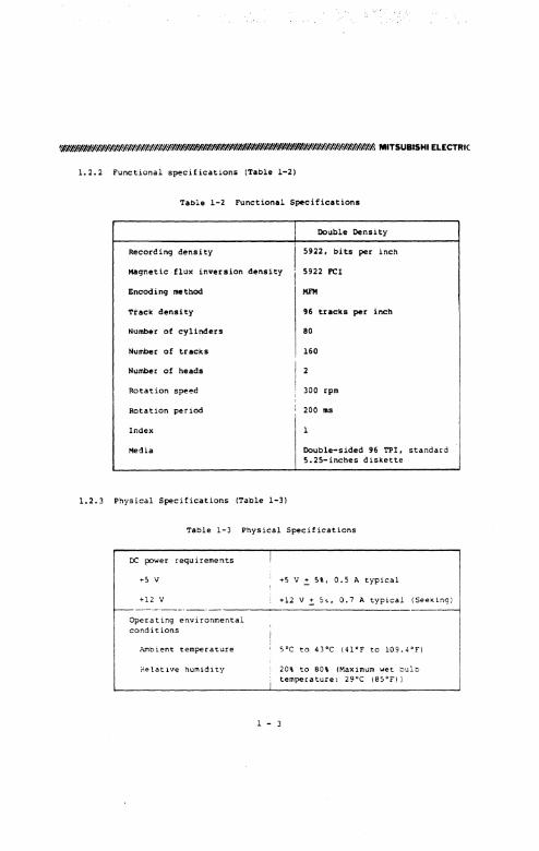
'111/111/1/1/1/1/1/1/1/1/1/1/1/1/1/111/1/1/1/1/111/1/1/111/111/1/1/1/111/1/1/1/111/1/1/1/1/1/1/1/1/1/1/1/1/1/1/1/1/1/1/1/1/1/1/111/1/1/1/1/111/1. MITSUBISHI ELECTRIC
1.2.2 Functlonal specifications (Table 1-2)
Table 1-2 Functional Specifications
Double Densi ty
Recording density 5922. bits per inch
Magnetic flux inversion density 5922 Fel
Encoding metllod MFM
Track density 96 tracks per inch
Number of cylinders 80
Number of tracks 160
Number of heads !
2
Rotation speed 300 rpm
Rotation period i 200 ms
Index I
I ~Ub1e-Sided 96 TPI. Media standard S.2S-inches diskette
1.2.3 Physical Specifications (Table 1-3)
Table 1-3 Physlcal Specifications
OC t=Ower requ i rements
+5 V +5 V!. 5%, 0.5 A typical
+12 V +12 V!. 5", 0.7 A typical (Seeklng)
Oper a t ing envi ronmental conditions
Ambient temperature
?I?'latllle humidlty 20% to 80% (Maximum wet. bulb temperature: 29"C (85°F))
1 - 3
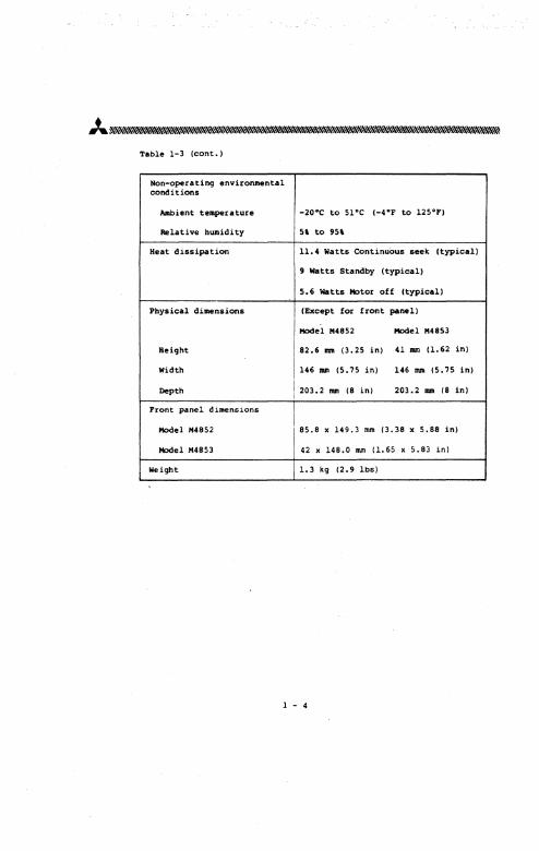
Table 1-3 (cont.)
Non-operati09 environmental conditions
Ambient temperature -20'C to 51°C (-4°F to 125°F)
Relative humidity 5' to 95'
Heat dissipation 11.4- Watts Continuous seek (typical)
9 watts Standby (typical)
5.6 watts Motor off (typical)
Physical dimensions (Except for front panel)
Model M4852 Model M4853
Height 82.6 nun (3.25 in) 41 nun (1.62 in)
Width 146 DIm (5.75 in) 146_ (5.7S in)
Depth 203.2 1M> (8 in) 203.2 mm (8 in)
Front panel dimensions
i Model M4852 8S.8 x 149.3 mm (3.38 x 5.88 in)
Model M48S3 42 x 148.0 mm (1.65 x 5.83 in)
Weight 1.3 kg (2.9 lbs)
1 - 4
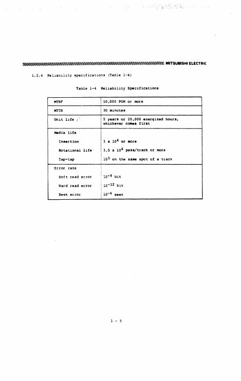
1.2.4 Reliability specifications (Table 1-4)
Table 1-4 Reliability Specifications
MTBF 10,000 POR or more
MTTR 30 minutes
Unit life : 5 years or 20,000 ener9ized hours, whichever COIle_ first
Media life
Insertion 13 x 104 or ODOre
Rotational life 3.S x 106 p ... /track or IIOre
I Tap-tap I 10 5 on the same spot of .. track
Error rate i Soft read error 1 10-9 bit
Hard read error 10-12 bit
Seek error 10-6 seek
1 - 5
'!/IIIIIIII//II//Ilil//IIIIII//IIIIIIIIIIII//IIIIIIIIIIIIIIIIIIIIIIIIIIII//I/r/lllllllllllllllllllll1//1111111111111111//111111//11//111111//111. MITSUBISHI ELECTRIC
CHAPTER 2 OPERATION OF MAJOR COMPONENTS
2,1 System Operation
The M48S2/M4853 Flexible Disk Drive consists of a medium rotating mechanism, two read/write heads, an actuato£' to plsition the read/wdte heads on tracks, a solenoid to load the read/write heads on the medium, and electronic circuits to read and write data, and to dr ive these components.
The rotation mechanism clam.ps the medium inserted into the drive to the spindle, which is directly coupled to the OC brushles, direct-drive motor, and rotates it at 300 rpm. The poSitioning actuator moves the read/write head over the desired track of the medium.. Then, the head loading solenoid loads the read/write head on the medium to read or write data.
2.2 Electronic Circuits
The electronic circuits to drive the individual mechanisms of the M4852/M48S3 are located on a single printed-circuit board, WhiCh consists of the following circuits:
o Line driver and receiver that exchange signals with the host_ system
a Drive selection circuit
o Index detection circuit
o Head positioning actuator drive circuit
o Head loading solenoid drive circuit
o Read/write circuit
o Write protect circuit
a Track 00 detection circuit
o Dr ive ready detect ion c ircui t
o Head selection c ircui t
o In use and panel indicator LED drive circuit
2 - 1
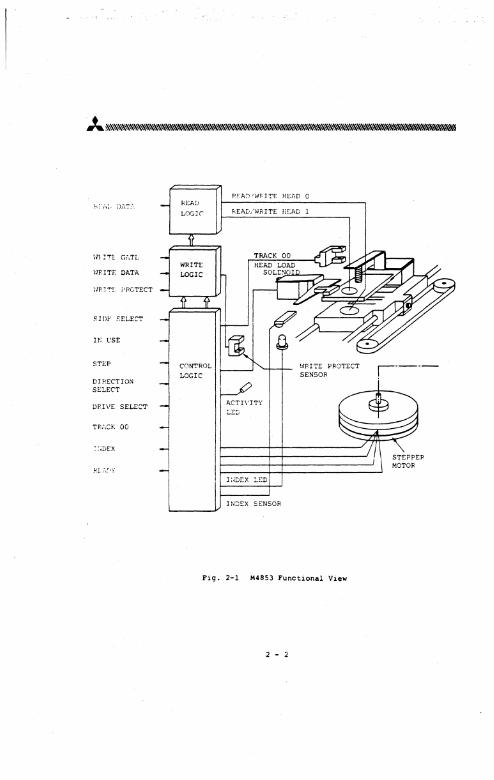
\'JF:ITE DATA
~IDi-' ::SLEC"!"
H: CSE
STEP
DIRECTION SE:LECT
DRIVE SELECT
TR,\SK 00
kEhU
LOGlr
WRITE
!-:EAD/''';:RITE Iif.:AD
ACTIVITY
I :~DLX :...ED
IN~£X SENSOR
~vPITE PROTECT SENSOR
Fig. 2-1 M4853 FUnctional View
2 - 2
(1#/1/1/1/#//1/#//1/1/1/1/1/1/1/1/1/1/1/1/1/1/1/1/1/#//1/1/1/1/1/1/1/1/1/1/1/1/1/1/1/1/1/1/1/1/1/1/1/1/1/#//#//1/1/1/1/1/1/1/1/1/1/1/1/1/4 MITSUBISHI ELECTRIC
2.3 Rotation Mechanism
The diskette rotation mechanism uses the OC brushless direct-drive motor to directly rotate the spindle at 300 rpm.
2.4 Positioning Mechanism
The positioning mechanism positions the read/write heads as deser ibed below.
The head carriage assembly is fastened to the steel band secured around the capstan of a two-phase hybrid stepping motor: a LBO turn of the stepping motor moves the read/we i te head one track in the designated direction, thus poSitioning the read/write head.
This drive system is temperature compensated to minimize read/write head deviations from the dirt tracks caused by ambient temperature change.
2.5 Reod!Write Heads
The read/write heads are MnZn magnetic ferrite.
Each read/write head has three ferrite head cores, consisting read/write core and erase cores on both sides of the read/write core to erase the space between tracks (tunnel erase).
The two read/write heads, which are located face-to-face with a disk. between them, are mounted on compliant, circular gimbal springs so that the heads track the disk. with good contact to enable maximum reproduction of the signals from the disk. The high surface tracking ability of the circular gimbal keeps the disk. free of stress, and thus improves diskette life.
2 - 3
WI/I/I/lPIIP/I/I/I/I/I/I/I/I/I/I/I/I/I/I/I/I/dI/I/I/dI/I/I/I/I/dI/I/I/I/I/Q//I/I/I/I/I/I/I/I/I/I/I/I/I/I/I/I/I/dI/I/I/I/I/I/I/I/I/I/lP, MITSUBISHI ELECTRIC
CHAPTER 3 ELECTRICAL INTERF ACE
There are two kinds of electrical interfaces: Signal interface and DC power interface.
The signal interface sends and receives control signals and read/write data between the M4853 and the host system via the JI/PI connector.
The DC power interface drives the spindle drive motor of the M4853, and supplies power to the electronic circuits and the stepping motor which drives the read/write head positioning mechanism via the J2/P2 connector.
The Signals and pin Arrangement of these two types of interfaces are shown in Tables 3-1 and 3-2.
Table 3-1 DC Power Connector Pin Arrangement (J2/P2)
SOurce vol tage Pin number Remarks
+12 V DC
I 1
! +12 ",J OC return 2 !
+5 V DC return 3
+5 V DC 4
3 - I
'I'able 3-2 Signal Connector Pin Arrangement (.1l/P1)
Signal 1 Signal Pln Number Ground Return Pin Number
SPARE
IN USE
DRIVE SELECT
INDEX
DRIVE SELECT 0
DRI VE SELECT
DRI VE SELECT
~lvTOR ON
DIRECTION SELECT
STEP
WRITE DATA
WRITE GATE
TRACK 00
WRITE PROTECT
READ DATA
S IDE ONE SELECT
READY I
10
12 11
14 13
16 15
18 17
20 19
22 21
24 23
26 25
28 27
30 29
32 31
34 33
3 - 2
r------------------- 3 m HA.X RIBBON OR TWISTED-PAIR CABLE
SIC~AL
1.0ST SYSTEM
L _____ --,-~ TERMINATOR
FDD No 4
DC 1"'(W .. 'ER
Fig. 3-1 Cabling Method (Sketch)
3.L2 Line driver and line receiver
The recommended interface line driver and line receiver circuits for the host system and the dr ives are shown in Fig. 3-2.
It is suggested that a Schmitt trigger circuit with a hysteresis characteristic at the switching level be used for the line receiver to improve the noise resistance of the interface lines.
,-------I "'I"5V
---------, : I 150nl/4W
SN7438N OR EQUIVALENT ~
D :r---Jo ,~ r-'=' !t ~
,h I I SN74LS14N OR • 5 V I I EQUIVALENT
l;:;won J,'4W I I SN7438~ OR I I EQUIVALENT
SNHLS14N OR 1). ~;:::====::;;~~: ====~~ EQUIVALENT ,.., ; I
H~ST_ S":S2:~ ~EC~~N _ J LM~8:: !~T-=~ __
Fig. 3-2 Recommended Line Dr iver and Line Receiver Circuits
3 - 4
fP/$#IIII'II#"#II",/#d/"II#'#IItW#II"I//d/"I/"I/I/I/I/#III/I/I/I/I/I/I/I/,I/I/I/I/I/I/I//#$//#1liiI/A MITSU8ISHI ELECTRIC
3.1 Signal Interface
The signal interface is classified into control signals and data signals. These interface signal lines are all at TTL levels. The meanings and character istics of the signal levels are oilS follows!
o True. L09ical "0" == VL 0 V to +0.4 V lin 40 rnA maximum
o False. Logical -1" • VB +2.5 V to +5.25 V Iin 0 IlIA
o Input impedance • 150 Ohms
3.1.1 Cabling me_thod and input line termination
The M4853 uses a daisy chain system of cable connections. A single ribbon cable or twisted-pair cable may be fitted with multiple connectors to permit connection of up to four drives.
The connected drives are multiplex-controlled by drive select lines, and anyone of the drives can be accessed.
The cabling method and input line termination are shown in Fig. 3-1. A maximum of seven input signal lines, plus the drive select lines, may be terminated at the M,4852/M4853. Proper operation of the drives requires termination at or near the drive connected to the end of the interface cable farthest from the host system.
The M4852 has detaChable resistor modules and M4853 has jumper plug terminators mounted on the printed-circuit board to terminate these input signal lines.
When a drive is shipped from the factory, its terminators are installed on the printed-circuit board.
Keep the terminators connected in the drive that is connected to the end of the interface cable, and disconnect the terminators in all the other drives.
3 - 3
W$III1PPlllIlIlIPlllllllllllllllllllddlllllllPIIlIl!l$lIlIlIldllIlIlIlIlIlIlIlIlIlIlIlIlIlIlIlIlIlIlIlIlIlIlIlI1I1IlIlIlIlIdldI#. MITSUBISHI ELECTRIC
3.1. 3 Jumpers
The jumpers on the printed-circuit board are used to set conditions for drive selection and head loading.
The uses of the individual jumper pins are as follows:
(1) MX
Jumper these pins when connectil\9 only one FOD to the system ..
The lingle drive then is always selected, permitting transmission and reception of input and output signals regardlels of the conditions of drive aelect 0 to drive select 3.
Open these pins when connecting two or more rODs.
(2) 050 to 053
When two or more rODs are connected to the system, jumper one of OSO to OS3 so that only the drive whose select line corresponds to the jumpered pin is selected by a logical "0" to petmi t transmission and reception of input and output signals.
For example, if 050 is jumpered. its drive is selected .... hen dr ive select 0 is at 109ica1 ·0.·
(3) as and I!M
These jumpers are used for setting head loading conditions.
If HS is jumpered, the heads are loaded by drive selection.
1 f liM is j umpered, the heads are loaded by turning the motor on.
Do not jumper KS and HM concurrently.
DSO and H5 are jumpered before shipment of the product from the factory. If different modes are desired, change the settings.
3 - 5
3.1.4 Input signal·lines
The M4852/M4853 has 11 input signal lines. Input signals can be classified into two types: One is multiplexed in a multi-drive system: and the other performs a multiplex operation.
The multiplexing signals are as follows:
o Or ive select
o Drive select
o Drive select
o Drive select 3
(1) Drive select 0 to drive select 3
When these dr ive select lines are at lQ9ical ·0· level, a mul tiplexed I/O lines become active to enable read/wr i te operation. These four separate input Signal lines, drive select 0 to drive select 3, are provided for connecting four drives to one system and mutually multiplexing them. Jumper pins 050, OSl, 052, and DS3 on the printed-circuit board are used to select drives to be made active, corresponding to dr i VEo select 1 ihes.
DSQ is shorted tJefore shipment from the factory, so this setting must be changed when establishing other select lines.
(2) Side one select
This interface line is used to select which of the two sides of the diskette should be read or written. When this line is at logical "1," the Side 0 head is selected; or when it is at logical "0," the Side 1 head is selected. If the polar ity of the sioe one select signal is reversed, delay read/write operation by more than 100 us before execution.
Upon completion of a write operation, reverse the polarity of the side one select signal after a delay of lOCO us. The heads are tunnel erase type, wi th a physical core gap aeviation between the read/write head and the erase heads so wi th no delay, non-erased areas would be generated on the diskette due to a timing difference between the write data area and the erase area during write operation. This is prevented by delaying the erase cur rent cutoff time of a few hundred microseconds within the M48S2/M4853. Therefore, the head select must not be reversed during this delay time. Also, the track access action must not be permitted for 1000 us.
3 - 6
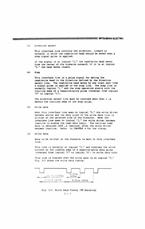
(3) Direction select
This interface line controls the direction. (inward or outward) in which the read/write head should be moved when a step signal pulse is applied.
If the signal is at logical "1," the read/write head moves from the center of the diskette outward: if it is at loqical "0," the head lIOVes inward •.
(4) Step
This interface line is a pulle 8ignal for moving the [ead/write head in the direction defined by the di[ection select line. The read/write head moves by one track each time a Signal pulse is applied to the step line. The step line is normally lQ9ical "1,· and the step operation starts with the trailing edge of a negative-going pulse (reversal from logical "D· to 109ical "1-'.
The direction select line must be reversed !lOre than 1 J,.:S
before the trailing edge of the step pulse.
(5) Write gate
When this interface line goes to logical ·0,· the write driver becomes active and the data given to the write data line is written on the selected side of the diskette. When the interface line goes to logical "1,· the write driver becomes inactive to enable the read data logic. The verifled read data is obtained 1000 ~s (maximum) after the write driver becomes inactive. Refer to CHAPTER 4 for the timing.
(6) Write data
Data to be wr itten on the diskette is sent to this interface line.
This line is normally at logical ·1," and reverses the write current at the leading edge of a negative-going data pulse (reversal from logical ·1" to logical "0") to write data bits.
This line is enabled when the write gate is at logical "0," Fig. 3-3 shows the write data timing.
4.0')ns i __ ~.::.2.::C.::O T: 21)Ons _~ .:.20ns--!
~E~)~_-=-~r.s 8.0Ci ... s .:.40n5
Fig. 3-3 Write Data Timing (FM Encoding)
3 - 7
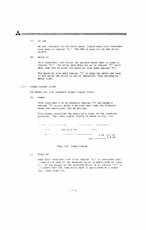
(7) In Llse
An LED Indicator on the front panel lights when this interface lIne goes tv logical "0." The LED is also lit by the drive select.
(8) Motor 0"
ThlS interface l.lnE' starts the spindle motor when it goes t<.. loglcal "0." The write gate does not go to logical "0" until more than 250 I'nS after the motor-on line goes logical "0."
The motor-on line goes logical "I" to stop the motor and keep it off while the drive is out of operation, thus prolonging motor life.
J.l. r, Output s1gnal lines
The M48S3 hdS f lye standard output Signal lines.
(1) Index
'This interface Lne is normally logical "1" but sends a logical "0" Olt'-t-"-"t pulse 4 ms wide eact: time the diskette makes one reVOll.ltlon (200 ms per iod).
This signal signifies the start of a track on the rotating diskette. The- :':1dex signal timing is shown in Fig. 3-4.
~--Ir- -----~
200.:3.2 inS
Fig. 3-4 Index Timing
i~) Track 00
,-----
4 ms n.o to B.O msi
:..,'hen this interface line is at logical "0," it indicates that :- read/write head of the selected drive is pJsitioned on track U'::'. If the output of the selected drive is at logical "1," It
J l,.J;'cat€'s that the read/write head is pJsitioned on a track {'l:;.h:' _ than tracK 00.
- 8
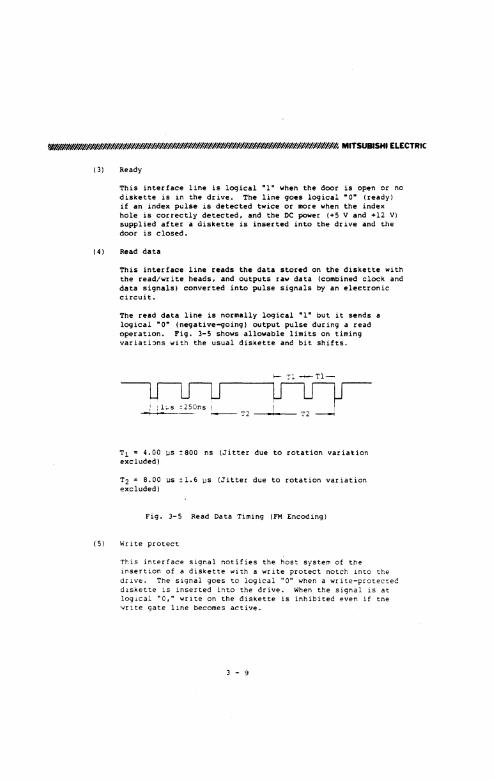
WP//############//###################//##########/Q/######################11. MITSUBISHI ELECTRIC
(31 Ready
This interface line is logical "1" when the door is open or no diskette is in the drive. The line goes logical "0" (ready) if an index pulse is detected twice or more when the index hole is correctly detected, and the DC power (+5 V and +12 V) supplied after a diskette is inserted into the drive and the door is c lased.
(41 Read data
This interface line reads the data stored on the diskette with the read/write heads, and outputs raw data (combined clock and data signals) converted into pulse signals by an electronic circuit.
The read data line is normally logical "l" but it sends a logical "0" (negative-goinq) output pulse during a read operatlon. Fig. 3-5 shows allowable limits on timing variati:ms with the usual diskette and bit shifts.
,
~-I -T2-...... --T2
Tl = 4.00 lJS ::800 os (Jitter due to rotation variation excluded)
T2 = B.OO lJS !1.6 lJS (Jitter due to rotation variation excluded)
Fig. 3-5 Read Data Timing (FM Encoding)
(5) Write protect
This interface signal notifies the host system of the insertion of a diskette with a write protect notch into the drive. The signal goes to logical "0" when a write-protectec dIskette 1S inserted into the drive. When the signal is at log..:..cal "0," write on the diskette is inhibited even if tne • ... rite gate l1ne becomes active.
3 - 9
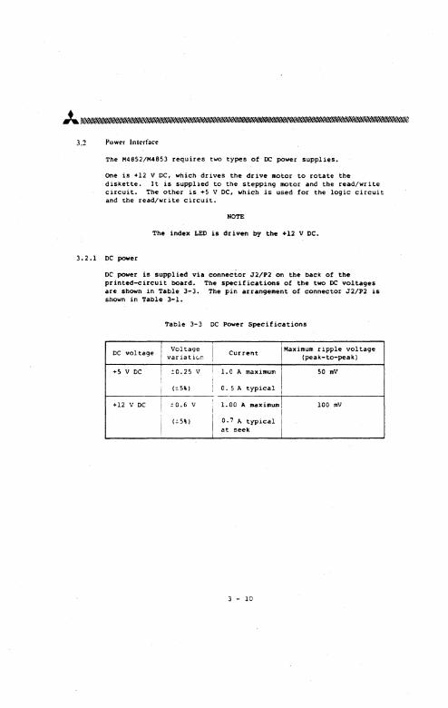
3.2 PowE."r IntE."rfacE."
The M4852/M4853 requires two types of DC power supplies.
One is +12 V DC, which drives the drive motor to rotate the diskett.e. It is supplied to the stepping motor and the read/write circuit. The other is +5 V DC, which is used for the logic circuit and the read/wr i te c ircui t.
NOTE
The index LEO is de iven by the +12 V DC.
3.2.1 DC power
DC power is supplied via connector J2/P2 on the back of the printed-circuit board. The specifications of the two DC voltages are shown in 'Table 3-3. The pin arrangement of connector J2/P2 is shown in Table 3-1.
Table 3-3 DC Power Specifications
I Volt.age I Maximum e ipple voltage DC voltage t Current i variati0l": i Ipuk-to-peak)
+5 V DC ! :0.25 V LOA maximum 50 mV i ;
i 1=5% ) ! O. 5 A typical I
+12 V DC i = 0.6 V t
1.00 A maXimum! 100 mV j
I ! I
1:5%) I 0.7 A typical i at seek I
3 - 10
~#/III#/II!##/II!#/III#####/III#/lIQ/IQ//I/lIQ/##/I/I/I/I/I#IQ/#/I##/I#/I/I/I/I#IQ/#/I/I/I/I/III/l1#h MITSUBISHI ELECTRIC
CHAPTER 4 FUNCTIONAL OPERATION
4.1 Power On Sequencing
No read/write operation may be performed during the period of 200 ma or more from the start of IX: power supply until the control Signal stabilizes and the dr ive is ready.
The read/write head may have been positioned on an incorrect track after switchif\9 the DC power on, so before atartinq a read/write operation, be sure to perform the step out operation until a track 00 signal is output to the interface line, and thus correctly poSition the read/write head.
4.2 Drive Selection
The M4852/M4853 daisy chain cablinq system permits connection of multiple drlves to a Single cable.
These drives are selected when the drive aelect lines on the drive side become active. Only the drive whose drive select line is active sends and receives signals to and from the host system. The select lines on the drive must have different numbers if two or more drives are connected. If the same number is aSSigned, an operation error occurs due to interference among the interface output signa.ls of the dr ives themselves.
4.3 Positioning Operation
The seek operation which moves the read/write head to the desired track selects a direction, inward or outward, depending on the polarity of the direction select signal, and moves the head by the step Signal. If access to a track two or more tracks away is required, step pulses are continuously sent until the head moves to the desired track.
Head movement starts with the trailing edge of the step pulse. Fig. 4-1 Shows the operation timing_
4.4 Side One Selection
The read/write heads located on both Sides of the diskette are sp.lected by the side one select signal. When the side one select line is high, the Side a head is selected. When it is low, the Side 1 head is selected.
4 - 1
4.5 Read Operation
The required t.iming for read operations is shown in Figs. 4-1 and 3-5. These timing specifications are necessary for accurate ['ead operation.
Two modes of encoding, PM and MFM, are used for the data stored on media. Fi .. is ·used for single-density read, and MFM for double-density read.
A comparison of the PM and MFM encoding modes is shown in FIg_ 4-2.
4.6 Write Operation
The requiring tilling for write operation is shown in Fig_ 3-3.
These timing specifications lIIust be strictly observed to ensure an accurate write operation.
Write data can be encoded by either PM or MFH. The H4852/H4853 has good contact stability of the read/write heads On the _dlum and employs high-performance read/write heads, so no precoaapensatlon is necessary for correcting the big shift effect when writing data in the MFH mode (double density).
In case of applying write precompensation, smaller compensation is recommended such as 7.5' or smaller.
4 - 2
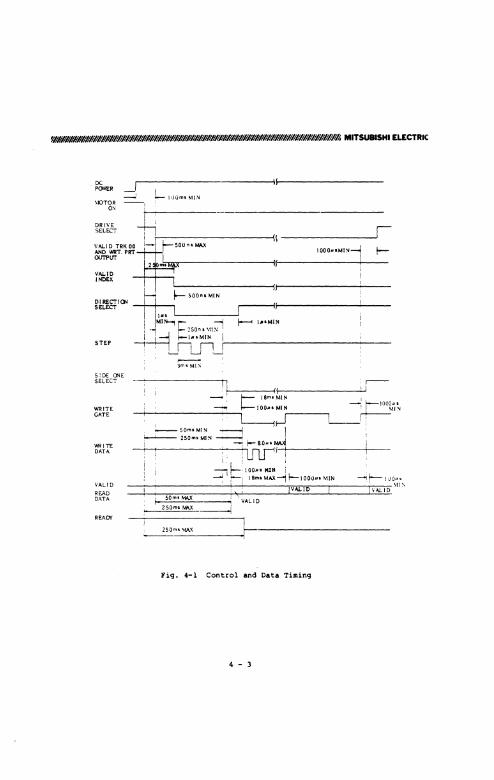
'1/1/1/1/1111//1/1/1/1/1/1/1/1/1/1/1/1/1/1/1/1/1/1/1/1/1/1/1/1/1/1/1/1/1/1/1/1/1/1/1/1/1/1/1/1/1/1111//1/1/1/1/1/1/1/1/1/1/1/1/1/1/1/1/1/1/1/1/1, MITSUBISHI ELECTRIC
DC ?CWER ~, I
-11)OmsMl,~
II
\iOTOR m.;
--,
DR!VE SELECT
! +i
I ~------------------~ VALID TRK 00 1- t--SOO"I MAX
IOOOi'IMI~j, AND WRT, PItT OOI'PlIf
VAJ..IO INDEX
DIRECT!()I/ SELECT
STEP
SIDE (NE SELECT
2 m~.~r-----------------~f----------------~----
~ IS ~i WRITE GATE
t= 18msMIN 1 -PIOQOUIi -r-~-------------'-""'; ! OOU 11041 N ,\\1 ~
~~. --==~~;:~~~~ --.J 1
"1< IT>: DATA.
VALID
READ DATA
REACII'
I ~ f-8..0-"'~ , Lflf"'11-+: ------!----I'; ;
1~:100MlMIN : --.i ri 18m'MAX~~1000"U\lIN
!VALID
50msMA.,X _ 'VALID
Z50m$M'..X ~
-"'I~l;JO"h i VA.LID ~1!"
250m! "M.'< f--------Fig_ 4-1 Control and Data Timing
4 - 3
~--,------,--,------,- ,-'I--r-DA1 A i ; i 1 : I J --L_~--''--LI_ "_---'----''--.1
DATA I J I J I J I 0 I 11 0 lot 0 I J I I
'ULJUL1LJULJL / MFM 1 / , /
/ /
/ /
/ /
/
/ /
/
/ /
/ /
Fig. 4-2 Compar ison of PM and MFM Encoding Systems
4 - 4
/ /
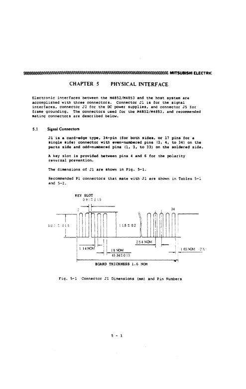
rt/IIA'IIIIIIIIIIIIIIIIIIIIIIIIII/IPIIII/IIIPIIIIII/IPIIPI/I/IIIIIII/IIIIIIIIIIII/IPIIIIIIIIIIIIIIIIII/IP1I1I/IPIIIIIIIIIIII/dI1I1I1I1I. MITSUBISHI ELECTRIC
CHAPTER 5 PHYSICAL INTERFACE
Electronic interfaces between the M4852/M4853 and the host system are accomplished with three connectors. Connector Jl is for the signal interfaces, connector .12 for the DC power supplies, and connector JS for frame grounding. The connectors used for the M4852/M4853, and recommended mating connectors are described below.
5.1 Signal Connectors
J1 is a card-edge type, 34-pin (for both sides, or 17 pins for a single side) connector with even-numbered pins (2, 4, to 34) on the parts side and odd-numbered pins (1, 3, to 33) on the soldered side.
A key slot is provided between pins 4 and 6 foc the polarity rev~rsal prevention.
The dimensions of .11 are shown in Fig_ 5-1.
Recommended Pl connectors that mate with J1 are shown in Tables 5-1 and 5-2.
KEY SLOT o 9 I :: G, 15
2 --j !-i ----
IO')-O=;5=!~~~~ I""" 1 i--I~!I i 1 14 NOM --i II~NOM I . 4534:::0.15
165NOM :?.\
I ... 1
BOARD THICKNESS 1. 6 NOM
Fig. 5-1 Connector Jl Dimensions (mm) and Pin Numbers
5 - 1
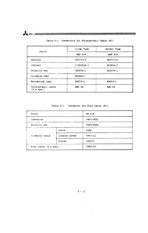
Table 5-1 Connectors for TWIsted-Pair Cable (PI)
I Cr imp Type I Solder Type Parts
AMP PIN AMP PIN
HousIng 583717-5 583717-5 1----------------
Contact 1-583616-1 583854-3 ---_. --_ ... _._._.----..-
PolarIty key 583274-1 583274-1 -- -- - .. --.---- --- ------+---
Cr implng tool i 90268-1 ------------ I Extraction tool 91073-1 ; 91073-1 -- --------- I
TWlsted-palr cable
i AWG 26
I AWG 26
(3 m max.)
Table 5-2 Connector for Flat Cable (Pl)
Parts 3M. PIN
Connector -1 3463-0001
-~~O~~~i~~_~eL ___ -r-___ ~~----o-o-oo-----------t I Press I 3440
Crimping tools Locator press 3443-11
3365/34 rl Platen
-- -- ----------'-----------+--------------1 Flat cable (3 m max.)
3442-3
5 - 2
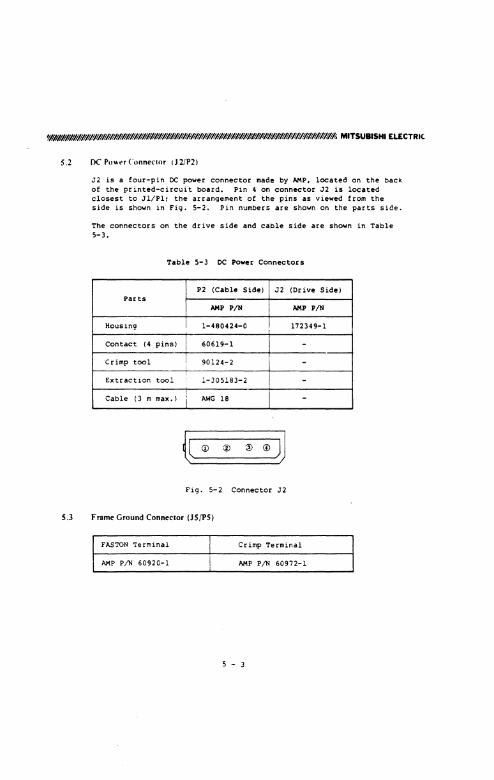
W/AI6WIII#IIII/IIII/I/I/I/I/I/lPI/P/I/III/I/III/lPI/P/I/I/I/I/I/I/I/I/I/I/I/I/III/I/I/III/I/I/I/III/I/III/III/I/I/I/I/I/I/I/I/I/I"dh MlTSUBISHI ELECTRIC
S.2 IK Po"" ("onnector IJ 2/P2)
J2 is a four-pin DC pow@or connector made by AMP, located on the back of the printed-circuit board. Pin 4 on conneetor J2 is located closest to Jl/P11 the arrangement of the pins as viewed from the side is shown in Fig. 5-2. Pin numbers are shown on the parts side.
The connectors on the drive side and cable side are shown in Table 5-3.
Table 5-3 DC Power Connector a
P2 (Cable Side) J2 (Drive Side) Parts
AMP PIN AMP PIN
Housin9 1-480424-0 172349-1
Contact (4 pins) 60619-1 -'Cr imp tool ! 90124-2 -Extraction tool 1-305183-2 -Cable (3 m max.) AWG 18 -
F 19. 5- 2 connector J 2
5.3 Frame Ground Connector (JS/PS)
FASTON Terminal Crimp Terminal
AMP PIN 60920-1 AMP PIN 60972-1
5 - 3
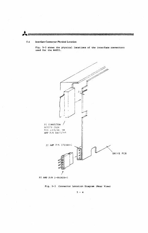
5.4 Interface Connectur Physical Location
Fig. 5-3 shows the physical locations of the interface connectors used for the "4853.
Pl CONNECTOR / SCOT(~H FLEX Pit; 3.,65/34. OR AMP FIN 583i17-5
J2 AMP P/l\ 172349-)
P2 AMP PIN 1-4b0424-D
I II
( II ,I
!I
Fig. 5-3 Connector Location Diagram (Rear View)
5 - 4
DRIVE PCB
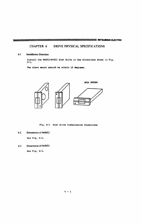
CHAPTER 6 DRIVE PHYSICAL SPECIFICATIONS
6.1 InstaUation Direction
Install the M4852/H4853 disk drive in the directions shown in Fig. 6-1.
The slant mount should be within 10 degree ••
Fig. 6-1 Disk Drive Inst.allation Directions
6.2 Dimensions of M48S2
See Fig. 6-2.
6.3 Dimensions of M4853
See Fig. 6-3.
6 - 1
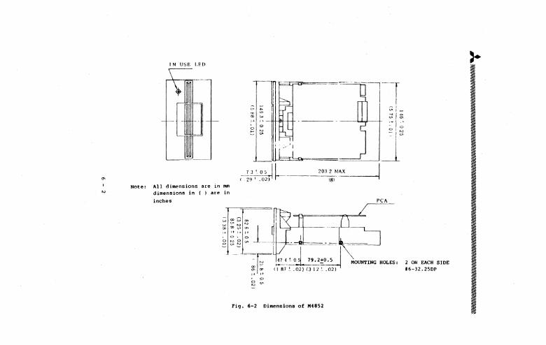
Notet
IN USE LED
ns are in mm All dlmenSl~n ( ) are in dlmenslons
inches
Fig. 6-2 f M4852 Dimensions 0
PCA
2 ON EACH SIDE t6-32.25DP
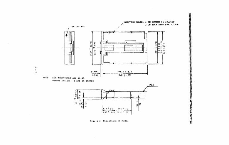
Note:
USE LED
'" :;: ~ "
1+ 1+
o
~ ~
14 MAX
(.55 )
All dimensions ace in mm dimensions in ( ) are in inches
/ MOUNTING HOLES.
--I~-l74 '0' 7" ' , 115
IIH7~.02) (ll:~'.02)
Fig. 6-3 Dimensions of H4SS)
ON BOTTOM 16-32.25DP ON EACH SIDE 16-32.25DP
peA
! ... c !!! ... = § '" n
CHAPTER 7 ERROR DETECTION AND CORRECTION
This chapter describes the general cause analysis and eorrective procedures to be followed in the event that data etrors occur.
7.1 Write Errors
If an error occurs during a write operation, it can be detected by performing a read operation on the diskette rotation lnnediately following the write operation. This i. generally called a write check, which is an effective means of pt'eventing write errors. It is recOllDlended, therefore, that a write check be lIade without fail.
If a write error occurs, repeat the write operation and conduct a write check. If data cannot be correctly written even after the write operation is repeated about ten timel, perform a read operation on another trAck to determine whether the data can be read correctly. If so, II specific track of the diskette is detective. If data cannot be correctly read on the other tr ack, the dr i ve is assumed to have some trouble. If the diskette is defective, replace it.
7.2 Read Errors
Most data errors that occur are soft errors. If a read error occurs, repeat the read operation to recover the data.
The following are possible main causes of soft errors:
o Dust is caught between the read/write head and diskette caUSing a temporary fault in head contact. Such dust is generally removed by the self-cleaning wiper of the jacket, and the data is recovered by the next re-read operation. If read/write is continued for a long time in a very dusty environment, however, hard errors can result from a damaged diskette surface.
o Random electrical noise ranging in time from a few microseconds to a few milliseconds can also cause read errors. Spike noise generated by a switching regulator, particularly one that has short switching intervals, deteriorates the signal-to-noise ratio, and increases the number of re-read operations for data recovery. It is necessary, therefore, to make an adequate cheCk on the noise levelS of the DC power supplies to the drive and frame grounding.
o Written data or diskettes may have so small a defect as cannot be detected by a data check during write operation.
o Fingerprints or other foreign matter on a written diskette can also cause a temporary error. If foreign matters is left on a
7 -
written diskette for a long time, it can adhere to the diskette, possibly causing a hard error.
It is recommended that the following read operations be performed to cor reet these soft er rors:
o Step 1:
o Step 2:
o Step 3:
o Step 4:
Repeat the read operation about ten times until the data is recovered.
If the data cannot be recovered by Step 1, move the head to other track, the opposite direction of the previous track position before the designated track, and then return the head to the original position.
Repeat an operation similar to Step 1.
If the data cannot be recovered, take the error as a bard error.
7 - 2

, I$l IIf' II)' IWIIPII/IAWlll/llPIIIIPIIII/IIIMIP#IIPllP/dlPlllI/IIIMIP#IIPIIII#P/IIIPIIPIIII/IP#II#IIIIPM MITSUBISHI ELECTRIC
CHAPTER 8 RESHIPMENT PRECAUTIONS
When teshippinq the drive, make sure the protection sheet for transportation is in place in the dr iva, and clos. the door.
8 - 1

MITSUBISHI ELECTRIC CORPORATION
MITSUBISHI ELECTRONICS AMERICA. INC. USA OFFICE tot' ... Oll. sr~HT TOIII~."Cl , ... _02 HI- ,2,31 ~'~"t93 T~~ &600'81 "'fV. T~"C
Specificetlc". subjeCt to eh,"V_ Without notiu Repn)duc1.1Ofl I"rohlilll.a
"&J2-G337S6-1s1 Edl!,on j .. nlil :982 ·SJ2·3J1SC·2r1d Edmon M.,c~ 1983
8303·700 A. S, 1<.. SB-S8€
APPENDIX C: TANDON RIGID DISK DRIVES - TM251, TM252
Tandon TM251, TM252 C-l
lanaon TM251, TM252
RIGID DISK DRIVES
-
PRODUCT SPECIFICATION AND USER'S MANUAL

NOTICE
Ttll:" document. and the information contained herein. is copyright by Tandon Corporation and may not be duplicated or reproduced. in whall' or in pan. without the prior writlen approval of Tandon Corporation.
Thl>; do~umem i~ intended \0 provide the u .. er with detailed information adequate for the efficient installation, operation. and sen ice of the equipment imohed.
Hm\~'\er. whiJt> e\'cr~ effort ha<. ~cen made to keep the information .:onlaincd herein current and accurate a<.. of Ihe dale 01 publi<,;<1110n, n0 guarantee i~ gi\en or implied as 10 it~ accuracy.
TM251, TM252 345 TRACKS PER INCH
PRODUCT SPECIFICATION AND USER'S MANUAL
I andan CORPORATION 20320 F'AAIAIE STREET
CHATSWORTH. CAUFORNIA 9131 1
© COPYRIGHT 1983 TANOON CORPORATION
Seclion Number Tille
CONTENTS
Page Number
SECTION I GENERAL DESCRIPTION
Introduction .............. .............................................................. ...... 1·1 1.1 Scope Of The Document ................................................................... 1·1 1.2 Purpose Of Th. Driv....................................................................... 1·1 1.3 Major Features ............................................................................... 1·1
Microprocessor Control................................................................. 1·1 Daisy Chain Capability.................................................................. 1·1 Industry Standard Int.rface Compatibility....... ................. ................. 1·1 Air Filtration.............................................................................. 1·2 Compact Size.............................................................................. 1·2
1.4 Functional Description..................................................................... 1·2 I.S Physical Description ........................................................................ 1·2
SECTION 2 PRODUCT SPECIFICATIONS
Introduction ..... ... ..... .... ............ ................ ....•............... ...... ....... .... ~-l 2.1 Mechanical Specifications ................................................................. 2·1 2.2 Electrical and Operational Specifications .............................................. 2·1 2.3 Reliability Specifications ................................................................... 2·1 2.4 Environmental Specifications............. ........................ ........................ 2·1
SECTION 3 OPERATION
Introduction.................................................................................. 3·1 3.1 Unpacking Th. Drive ....................................................................... 3·1 3.2 Preinstallation Checkout .................................................................. 3·1 3.3 :.'lounting The Drive ........................................................................ 3·1
Dust Cover ................................................................................. 3·2 Free Air Flow.............................................................................. 3·2 Confined Environment .................................................................. 3·2
3.4 Interface Connectors...... ........... ........................... ............ ........ ....... 3·2
3.5
3.6 3.7
J I/PI Connector......... ............... .......................... ........ ........ ....... 3·2 J2/P2 Connector....... ............ .... .... .... ........ .... .... ........... ......... ...... 3-2 J3/P3 Connector ........................................................................ , 3-~ Frame Ground Connector.............................................................. 3·2
Interface Line Descriptions ......................................................... _...... 3-6 Input Control Signals.................................................................... 3-6 Output Control Signals .................................................................. 3·11 Data Transfer Signals.......................................................... 3·12
Drive Address and Option Sekction ..................................................... 3·13 Shipping Pack and Handling .............................................................. 3·13
Figure Number
1·1 2·1 2·2 3·1 3·2 3·3 3·4 3·5 3·6 3·7 3·8 3·9 3·10 3·11 3·12 3·13 3·14
T.ble "umber
2·1 2·2 2~3
3·1 3·2 3·3
ILLUSTRA TIONS
FIGURES
Title Page
Number
Disk Drive .................................................................................... . Disk Drive Outline Drawing .............................................................. . Typical Starting Currents ................................................................. . Multipack Shipping Cont.iner .......................................................... . J I Edge Connector Dimensions ................................................... , ..... . J2 Edge Connector Dimensions ......................................................... . J3 Power Connector. ...................................................................... . Radial Configuration ...................................................................... . Daisy Chain Control Lines ............................................................... . Control SignallDriver Receiver Circuit Combination .............................. . Step Mode Timing .......................................................................... . Buffered Seek Step Pulses ................................................................ . Data Transfer Line Driver Receiver .......... , '" ...................................... . Recommended Shipping Pack Design, Configuration I .......................... .. Recommended Shipping Pack Design, Configuration 2 ........ . Recommended Shipping Pack Design, Configuration 3.. .. . Load Graph .............................................................. ..
TABLES
1·2 2·2 2·5 3·3 3-4 3-4 3-4 3·7 3·8 3·9
3·10 3·10 3·12 3·15 3·17 3·18 3·20
Titl. Page
~umber
Electrical and Operational Specifications Reliability Specifications.... . .............. . Environmental Specifications ................ . Drive Interface Signals and Pin Assignments ........ . Head Select Lin" ... Option Programming Guide ..
2·3 2·6 2·7 3·5 3·9 3·14
SECTION 1
GENERAL DESCRIPTION
INTRODUCTION
This manual provides useful information to assist the customer when incorporating the Tandoo rigid disk drive into a system.
Tandoo Corporation's TM250 series of drives are full feature. one-half height. 5-I/4-inch. rigid disk drives. They are compact data storage devices that contain one or more l30-millimeter plated aluminum platters within a scaled housing.
The TM250 series includes Model Numbers TM251 and TM252. which have one or two recording platters, and use two or four recording heads, respectively.
1.1 SCOPE OF THE DOCUMENT
Section I of this manual contains a general description of the disk drives. Section 2 contains the product specifications. Section 3 provides information on operation of the drives.
1.2 PURPOSE OF THE DRIVE
The 5-1/4-inch disk drive is a rotaling disk memory device designed for random access data storage and retrieval. Typical applications include word processing systems, entry level microprocessor systems. intelhgent calculators, program storage. small business computer systems. and any application in which low cost, random access data storage is required.
I-I
1.3 MAJOR FEATURES
MICROPROCESSOR CONTROL
The TM2S0 series of drives feature an on board microprocessor. The microprocessor provides five major functions:
l. Self-calibration on power-up.
2. Buffered seek timing for improved access times.
3. Improved positioning with reJu..:ed hysteresis.
4. Write current switching for optimal recor· ding quality.
5. Power and track fault detection.
DAISY CHAIN CAPABILITY
The drive provides the address selection and gating functions necessary to daisy chain a maximum of four units at the user's option. The last drive on the daisy chain terminates the interface. The ter· minations are accomplished by a resistor array plugged into a DIP socket.
INDUSTRY STANDARD INTERFACE COMPATIBILITY
The drive is compatible with (omrollers that use an industry standard interface.
AIR FILTRATION
A self-contained. recirculating air filtration system supplies clean air throug.h a O.3-micron fiiler. A secondary absolute filter i~ pro\'ided to allow pressure equalization with the ambient almosl"here without conramination. The entire head-disk-actuator compartment is maintained at a slightl).' positive pressure to fUMher ensure an utraclean en\.'ironment.
COMPACT SIZE
The reduced height qf the drh,e occupies only onehalf the mounting space required for a conventional drive.
1.4 FUNCTIONAL DESCRIPTION
The drives are fully self-contained. and require no operator intervention during normal operation. During the po"er-ur sequence, th~ spindle motOr reaches 3.600 RPM. and the positioning mechanism recaJibrates the recording heads to Track O. Al thi~ time. a Ready !lignal on the interface indicate~ the drhe i!i ready for operation.
The head is positioned over the desired track by means of a four-phase stepfler mOler/band assembly and its as~ocjat('d electronics. This positioner use~ a one-step rotation to cause a one-track radial movement. Subsequently, the recording head!' can be positioned over the desired cylinders. and the data can N read or written from the appropriate track hy selecting the desired head.
Typically. the dri\e uses \1FM write and read data recording methods. Data recovery electronics include a lo\\-Ie\'el read amplifier, differentiator. a zero-cro!O!.over detector. and diBitizing circuits. No dala encoding or decoding feature is provided on the driH's.
The drives ha\c the following: sensor systems:
1. An optical Track 0 ~WilCh sense, when the Head 'Carriage As!'!embly i, positioned at Tra,-k O.
1-2
2. An index sensor. which consists of a magnetic pick-Up and inde-.: hole positioned to provide an analog signal when an index hole is detected.
1.5 PHYSICAL DESCRIPTION
A representative drive is. shown in Figure I-I. The drives contain 130 millimeter storase media that rotate at 3.600 RPM. using a direct drive, brush less D. C. mOlor, The recording. is accomplished by non-contact standard recording heads that are moved by a precision split band positioning device and stepper motor.
FIGURE 1-1 DISK DRIVE
The Head Disk Assembly is enclosed in a sealed cast aluminum housing, which includes an air filtration system to ensure a contamination·free environmcnt. The housing is shock mounted to a metal frame that has the front panel attached. and threaded holes on the sides and bottom for mounling the drive onlO a chassis.
In addition, the drive includes the read/write and control electronics. servo spindle control elec· tronic~. and an inde;.. sensor.
SECTION 2
PRODUCT SPECIFICATIONS
INTRODUCTION
This section contains the mechanical and operational, reliability and environmental specifications for the TM25 I and TM252 disk drives.
2.1 MECHANICAL SPECIFICATIONS
The mechanical and physical dimensions are contained in Figure 2~ I.
2.2 ELECTRICAL AND OPERATIONAL SPECIFICATIONS
The eiectril.:al and operational ~pel:ifi.:ations are contained in Table 2-1. Typical staning current requirements at nommal .... oltage are comained in Figure 1-2.
2.3 RELIABILITY SPECIFICTIONS
The reliability specifications are \:ontained -in Table 2·2.
2.4 ENVIRONMENTAL SPECIFICATIONS
The environmental specifications are contained in Table 2-3.
I an aiiil CORPORATION. CHATSWORTH. CALIFORNIA 91311
2-1
179050·001 REV. A.
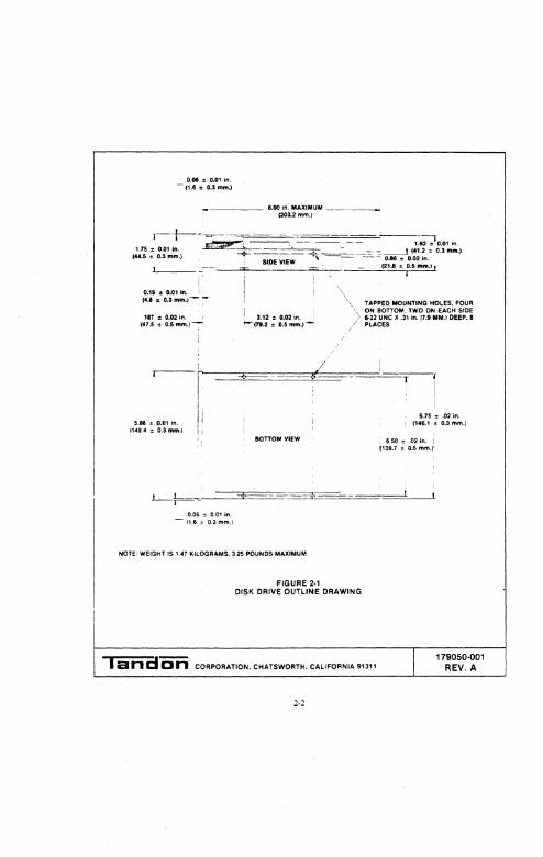
0.06 or 0.01 in. - 11.6 or 0.3 mm.}
_____ 8.00 In. MAXIMUM _____ _
0." : 0.01 m. (4.8 :r; 0.3 mm.) -- -
117 :r; 0.02 In. (47.5 : 0.5 mm.) -:--'
r-r I
S.U :to 0.01 in. ! (149.4 :to 0.3 mm.) ! i
0.06 :t 0.01 in. (1.6 .:!: 0.3 mm.)
(20l.2mm.)
3.12 or 0.02 in. J-- (11.2 : 0.5 mm.) ~
I ..
BOTTOM VIEW
NOTE: WEIGHT IS 1.47 KILOGRAMS. 3.25 POUNDS MAXIMUM
FIGURE 2·' DISK DRIVE OUTLINE DRAWING
TAPPED MOUNTING HOL.ES. FOUR ON BonOM. TWO ON EACH SIDE 6-32 UNC X .31 in. (7.9 MM.) DEEP. 8 Pl.ACES
T
5.75 :to .02 in. ! 1146.1: 0.3 mm.)
5.50 :t .02 in. :(139.7 :t 0.5 mm.)
I an Cliiii CORPORATION. CHATSWORTH. CALIFORNIA 91311 I 179050·001
REV. A
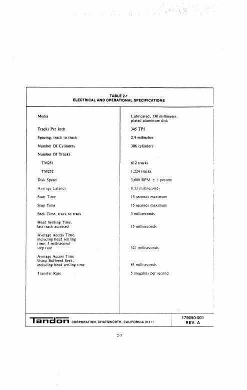
TABLE 2·1 ELECTRICAL AND OPERATIONAL SPECIFICATIONS
Media
Tracks Per Inch
Spacing, track to track
Number Of Cylinders
Number Of Tracks
TM251
TM252
Disk Speed
Average Latency
Slart Time
Stop Time
Seek Time, track to track
Head Settling Time, last track accessed
Average Access Time. induding head settling time, 3 millisecond step rate
Average Access Time Using Buffered Seek, including head settling time
Transfer Rate
Lubricated. 130 millimeter. plated aluminum disk
345 TPI
2.9 milinches
306 cylinders
612 tracks
1,224 tracks
3.600 RP,l " I percent
15 seconds maximum
15 seconds maximum
3 milliseconds
15 milliseconds
321 milliseconds
85 milliseconds
5 megablls per ~econd
I an Cliiil CORPORATION. CHATSWORTH. CALIFORNIA 91311 i
2·}
179050·001 REV. A
I
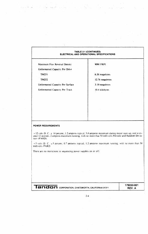
TABLE 2·1 (CONTINUED) ELECTRICAL AND OPERATIONAL SPECIFICATIONS
Maximum Flu.\ Reversal Density 9090 FRPI
Unformatted Capacity Per DrivE':
TM251 6.38 megabytes
TM252 12.76 megab}1eS
Unformatted Capacity Per Surface 3.]9 megabytes
Unformaued Capacity Per Track 10.4 kilobytes
POWER REOUIREMENTS
..... 12 volt:. D. C. == 10 per..:ent, 1.2 ampere~ typi(al. 3.6 amperes maximum during motor stan-up, nOI to exceed J~ :.ewnd~, 2 amperes maximum running. \\J!h no more that 50 milli\'ohs Periodic and Random Deviation (PARD).
... ~ \olt" D. C. =5 pen:ent, 0.7 ampere~ typical, 1.2 ampere ... ma\imum funning. with no more than 50 milli\"o!t\ PARD.
There are no resnictiom in :.equcncing power supplic:, on or off.
I an aiiii CORPORATION. CHATSWORTH, CALIFORNIA 91311
2-4
179050·001 REV. A
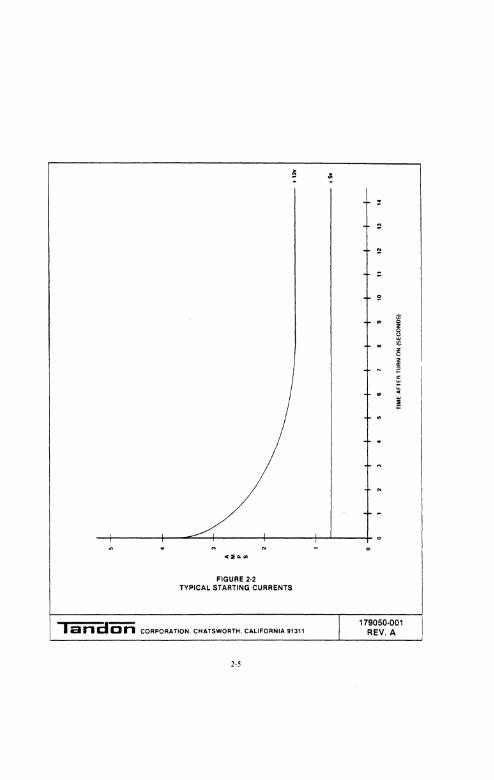
~ olI + +
::
l!
l!
;:
l!
~ Z 'I
" Ie z Q z '" ;: " "' :. c
"' !
I FIGURE 2·2
TYPICAL STARTING CURRENTS
I I an a'ii'n CORPORATION. CHATSWORTH. CALIFORNIA 91311 I 179050·001 I
REV. A
2·5
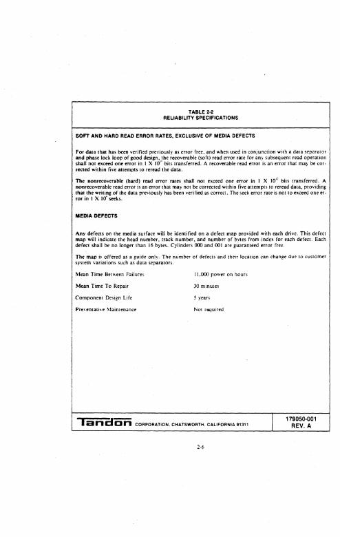
TABLE 2·2 RELIABILITY SPECIFICATIONS
SOFT AND HARD READ ERROR RATES, EXCLUSIVE OF MEDIA DEFECTS
For data that has been verified previous)} as eTTor free. and when used in conjunction v.'ilh a data separator and phase lock loop of good design, the recoverable (soft) read error rate for an~ subsequent read operation shall not exceed one error in I X 10 1
" bits transferred. A recoverable read error is an error thaI may be cor· reeled within five anempts to reread the data.
The nonrecoverable (hard) read error rates shall nOl exceed one error in I X IOI~ bils transferred. A nonrecoverable read error is an error that may not be corrected within five attempts to reread data. providing that Ihe writing of the data previously has been verified as correct. The seek error rate is nOi to exceed one er~ ror in I X 10" seeks.
MEDIA DEFECTS
Any defects on the media surface will be identified on a defect map provided with each drive. This defect map will indicate the head number, track number. and number of bytes from index for each defect. Each defect shall be no longer [han 16 bytes. Cylinders 000 and 001 are guaranteed error free,
The map i!' offered as a guide only, The number of defects and their location can change due to customer system \'anatiom such as data separaton.,
Mean Time Betv.een Failures 11,000 power on hours
Mean Time To Repair 30 minutes
Component DeSign Life 5 years
Pre\:entati"e Maintenance Not rllquired
I an a"i5ii CORPORATION. CHATSWORTH. CALIFORNIA 91311
2-6
I 179050·001
REV. A
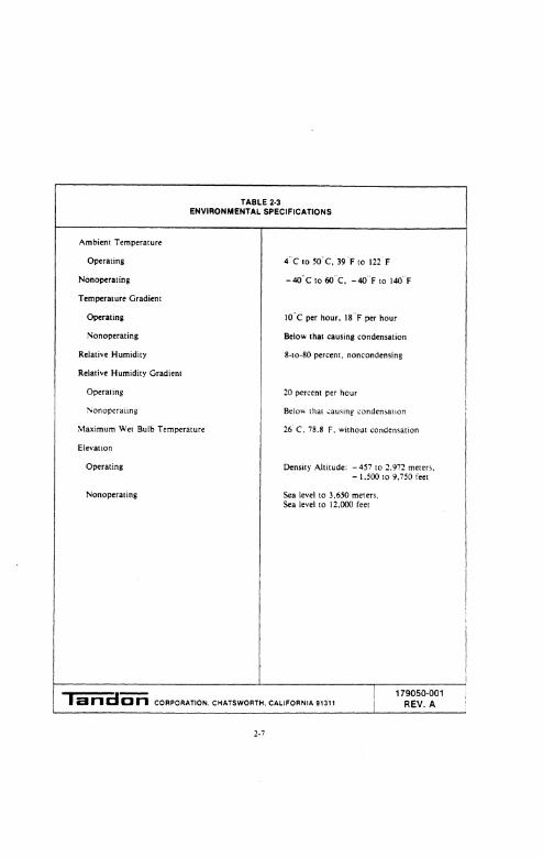
Ambient Temperature
Operating
Nonoperating
Temperature Gradient
Operating
Nonoperating
Relative Humidity
Relative Humidity Gradiem
Operating
~onoperat!ng
TABLE 2·3 ENVIRONMENTAL SPECIFICATIONS
4 C 10 50' C, 39 'F 10 122 F
-4O"C 10 6O"C, -4O"F 10 14O"F
IO'C per hour, 18 F per hour
Below that causing condensation
8-tO-80 percent, noncondensing
20 percent per hour
Belo~ that ..;au:o;mg condensatIon
Maximum Wet Bulb Temperature 26 C. 78.8 F, without condensalion
Elevation
Operating
Nonoperating
Density Altitude: -457 to ~.9n meters, - 1.500 10 9.750 feet
Sea level to 3.650 meIers, Sea level to 12.000 feet
I an a'ii'ri CORPORATtON. CHATSWORTH. CALtFORNtA 91311 i 179050·001
REV. A
SECTION 3
OPERATION
INTRODUCTION
This section contains information pertinent to the handling. inspection. installation, and operation of the TM250 series of drives.
3.1 UNPACKING THE DRIVE
Each drive is shipped in a protective container which, when bulk packaged. minimizes the possibility of damage during shipment.
The following procedure is recommended for un· packing the drive.
I. Place the shipping container on a nat work surface.
2. Visually examine the shipping container for damage.
3. Cut the tape on the shipping container.
4. Remove the foam lid and pads from the shipping container.
5. Remove the inner container.
6. Remove the drive from the inner container.
7. Place the drive on a foam lined surface.
8. Notify the carrier immediately if any damage is found.
CAUTION
Do not manual!. ... rotale the stepper motor or spindle motor. Damalle 10
the heads and disk may result.
3·1
NOTE
The inside chamber of the drive is a sealed compartment that must not be opened.
When returning the drive to the service center. be sure to use prior steps in reverse order. and ensure the foam stiffeners are in the proper location. with the cardboard dividers properly in place bet\\.oeen the drives (see Figure 3·1).
3.2 PREINSTALLATION CHECKOUT
Before applying power to thoe drive. inspect for the following:
I. Ensure the front panel is secure.
2. Ensure the circuit board is secure.
3. Ensure the connectors are firmly sealed.
4. Ensure there is no debri!> or foreilln material between the frame and [he head/disk casting.
5. Ensure the head/disk housinE can move freely on the shock mounts of the frame.
6. Ensure the termination resistor pack and jumper blocks are firmly seated and in the correct configuration.
3.3 MOUNTING THE DRIVE
The dri .... e can be mounted in am \'ertical or horizontal plane. Eighl 6~32 lapped holes are pro\ided for mounting: two on each <;jde and four on the bottom of the frame isee Figure 2·1 t. The drive
i~ manufactured with some' critical internal ali!!nmenn, that must be maintained. Hence. it is important the mounting hardware does not introduce significaOi stress on the drive.
An~ mounting scheme in which the drive is part of the structural integrity of the enclosure is not permitted. Mounting schemes should allow for adjustable bra~kets or incorporate resilient members to accommodate tolerances.
DUST COVER
The design of an enclosure should incorporate a me-am. to prevent contamination from loose items, e. g.., dust, lint. and paper chad since the drive doe~ nOI have a dust cover.
FREE AIR FLOW
When the drive is mounted so the components have aCce<iS to the free now of air. normal conveclion cooling allows operation over the specified temperature range (see Table 2-3).
CONFINED ENVIRONMENT
When the drive is mounted in a confined environment, air now must be provided to maintain ~red:-ied air temperatures in the vicinity of the molor" and !ht' 1.;'1rCUil boards.
3.4 INTERFACE CONNECTORS
The electrical interface between the drive and the host system i~ ,ia three conneClOrs. J I provides control signal~ for the drive (see Figure 3-2). J2 prmide ... for the radial connection of read1write data ~ig:nall; (~ee Figure 3-3). B provides for D. C. power (.,ee Figure 3-4).
3·2
Table 3-1 contains interface lines. The interface description of the conneclOrs, and the location of each. is contained in this seclion.
J1/P1 CONNECTOR
Connection to J I i,s through a thirty-four-pin connector. Figure 3-2 comains the dimensions of this connector. The pins are numbered J through 34. The recommended mating connector for PI is AMP connector PIN 499496-9.
J2IP2 CONNECTOR
Connection to J2 is through a 20-pin connector. Figure 3-3 contains the dimensions of this connector. The recommended mating conneClor for P-2 is AMP connector PIN 499497-4.
J3/P3 CONNECTOR
D. C. power connector 13 is a four-pin AMP Mate-I'-Lok connector, PlY" 350211-1. moumed on the componenl side of the circuit board. The recommended mating connector, P3. is AMP P/N 1480424·0. utilizing AMP pin, P'N 606194. J3 pin~ are labeled on the J3 conneCior (see Figure 3-4).13 .:abJing: mUSI be 18 AWG, minimum.
FRAME GROUND CONNECTOR
The frame ground connector is Faslon AMP P/N 61761-2. The recommended mating connector is AMP P/N 6218i-l. To realize error rates (see Table 2-2). il must be connected directly to the centrally located system ground via an 18 AWG, minimum. cable.
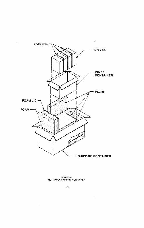
DRIVES
INNER CONTAINER
FOAM
SHIPPING CONTAINER
FIGURE 3·1 MULTIPACK SHIPPING CONTAINER
J·3
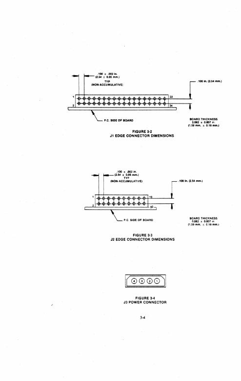
33
..
FIGURE 3·2 Jl EDGE CONNECTOR DIMENSIONS
..
FIGURE 3·3 J2 EDGE CONNECTOR DIMENSIONS
FIGURE 3·4 J3 POWER CONNECTOR
3-4
.100 In. (2.54 mm.)
BOARD THICKNESS 0.062 ::t 0.007 in.
(1.51 mm. :.t 0.18 "'11:'.)
.100 In. (Z.s. mm.)
BOARD THICKNESS 0.082 ::t 0.007 in,
(' .59 mm. ::t 0.'8 mm.)
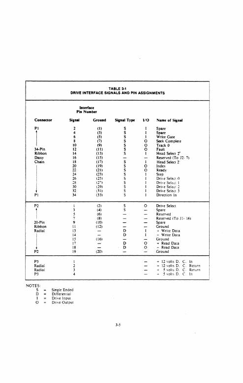
TABLE 3-1 DRIVE INTERFACE SIGNALS AND PIN ASSIGNMENTS
Interf .... PI. Number
Connector Sianol Ground
PI
I 34-Pin Ribbon Daisy Chain
I j
PI
P2
1 20-Pin Ribbon Radial
1 P2
P3 Radial Radial P3
NOTES: S o 1 o
2 4 6 8 10 12 14 16 18 20 22 24 26 "8 30 32 34
1 3 S 7 9 11 13 14 IS 17 18 19
1 2 3 4
Single Ended Differential Drive Input Drjl.:e Output
(I) (3) (S) (7) (9)
(11) (13) (IS) (17) (19) (21) (23) (2S) (:!") (29) (31) (33)
(2) (4) (6) (8)
(10) (12) --
(16) --
(20)
Signal Type 1/0 Name of Signal
S I Spare S I Spare S I Write Gate S 0 Seek Complete S 0 Track 0 S 0 Fault S I Head Select 2' - - Reserved (To 12- 7) S I Head Select 2' S 0 Index S 0 Ready S I Step S I Drive Select 0 S I Dri .. e Se1e.:r 1 S I Dri\ e Sel.:.:! : S I Drive Select 3 S I Direction In
S 0 Drive Select S - Spare - - Reserved - - Reserved (To Jl- 16) - - Spare - - Ground 0 I + Write Data 0 1 - Write Data - - Ground 0 0 + Read Data 0 0 - Read Data - - Ground
- -+ 12 volts D. C. In - + 12 vol15 D. C. Return - + 5 ... olt~ D. C. Return - + 5 volls D. C. In
3-S
I
I i
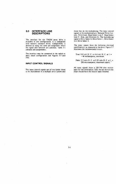
3.5 INTERFACE LINE DESCRIPTIONS
The imerface for the TM2S0 series drive is available in one config.uration. II is compatible with industry standard drives. Compatibility is defined as using the !i.ame pin assignment where the signal and [unction are common. Table 3·) contains pin assignments.
The interface may be connected in the radial or dais), chain configuration (see Figures 3·5 and 3-6).
INPUT CONTROL SIGNALS
The input control signals are of two kinds: those to be multiplexed in a multiple drive system and
3-6
those that do the multiplexing. The input control signals to be multiplexed are: Reduced Write Current, Write Gate, Head Select Line 2", Head Select Line 2', Step. and Direction In. The multiplexing signal is Drive Select O. Drive Select I, Drive Select 2 or Drive Select 3.
The input signals have the following electrical specification'l, a~ measur.ed al the drive. Figure 3-7 illustrates the recommended circuit.
True: 0.0 volt D. C. to 0.4 volt D. C. at I = - 40 milliamperes, maximum
False: 2.5 volts D. C. to 5.25 volts D. C. at I = 250 microamperes, maximum (open) (
All input signals share a 220/330 ohm resistor pack for line termination. Only the last drive in the chain should have the resistor pack installed,
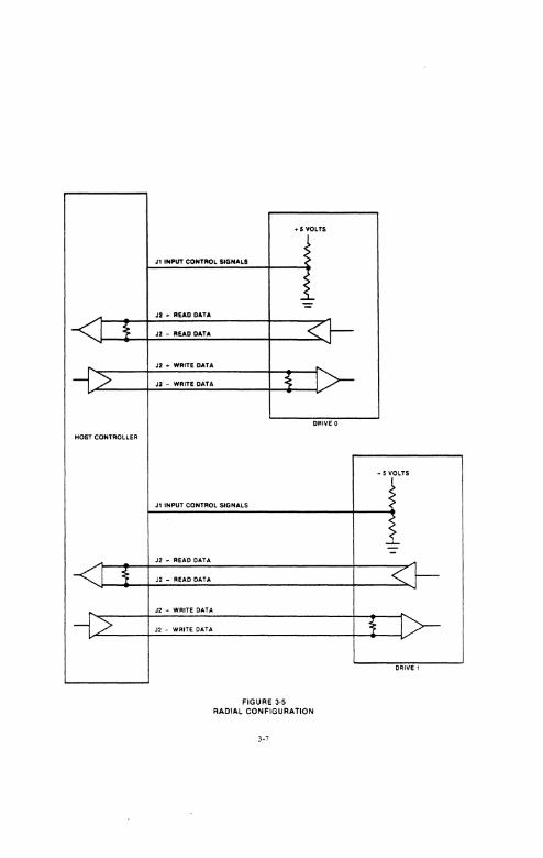
I ~
>
HOST CONTROLLER
I ~
>
... 5 YOLTS
J1 INPUT CONTROL SIGNALS ;>
: -=
J2 ... READ DATA
J2 - READ DATA < '"
J2 .. WRITE DATA ..... J2 - WRITE DATA ~ I
DRIVE D
J1 INPUT CONTROL SIGNALS
J2 • READ DATA
J2 - READ DATA
J2 ... WRITE CATA
J2 - WRITE CATA
FIGURE 3·5 RADIAL CONFIGURATION
3·7
+5 VOLTS
;>
> :--<
~ I
DRive 1
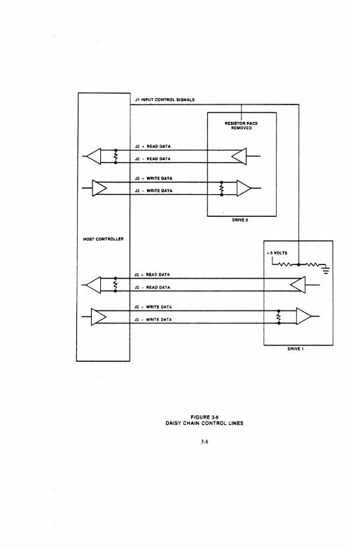
J1 INPUT CONTROL SIGNALS
I
REStSTJ .. PACK REMOVED
J2 + READ DATA
I { J2 - READ DATA < J2 + WRITE DATA
> n - WRITE DATA ~ I
DRIVE 0
HOST CONTROLLER
-+ 5 VOLTS
L -= J2 + READ DATA -
I i J2 - READ DATA < J2 .... WRITE OATA "-
> J2 - WRITE DATA ~ I ~
DRIVE 1
FIGURE 3·6 DAISY CHAIN CONTROL LINES
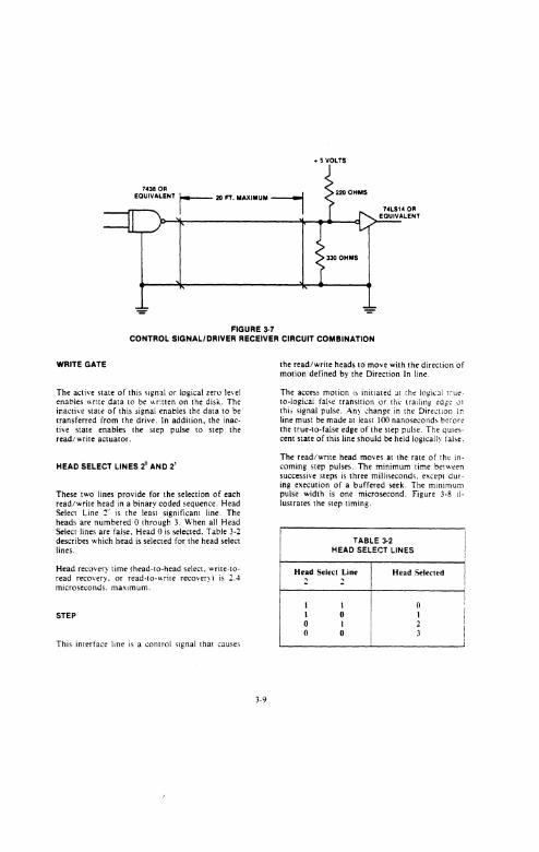
.... S VOLTS
1438 OR
__ .rrE_Q_U_'V .... ALENT I"'"· MAXIMUM "I
FIGURE J.7 CONTROL SIGNAL/DRIVER RECEIVER CIRCUIT COMBINATION
WRITE GATE
The active state of this <;ign:li or iogicalzero le\ el enables wme data to be \\fitten on the disk. The inacul,.e state of this signa! enables the data to be transferred from the drive. In addition. the inactive state enables the step pulse to step the read/write actuator.
HEAD SELECT LINES 2' AND 2'
These two lines prOVide for the selection of each read/write head In a binary coded sequence. Head Select line 1" is the least Significant line. The heads are numbered 0 through 3. When all Head Select lines are false. Head 0 is selected. Table 3-2 describes which head is selected for the head select lines.
Head reco ... erv time (head-Io-head select. write-toread recovery. or read-to-wrile reco ... ery) is ~.-l microseconds, maxImum.
STEP
ThiS interface hne IS a control signal that causes
)-9
the read/write heads 10 move with the direction of motion defined by the Direction In line.
The access motion i~ initIated :iI the lo~i';31 t~ut:'to-logical fal"e transition or Ih..: {ra!lHl-~ ~a.;:: 01 thi:) signal pulse. An~ ~hange in the Dtre.:uon if; line must be made at least 100 nanosecond!. berort:: the true-to-false edg.e of the step pulse. The qUlc~cent state of this lme should be held loglcall~ fal~e.
The read/write head moves at the rate of Ihl: incoming step pulses. The minimum time bet\\t:en successive steps is three milliseconds, excepI during execution of a buffered seek. The mInimum pulse width is one microsecond. Figure 3-8 Illustrates the step timing.
TABLE 3-2 HEAD SELECT LINES
Head Select Line Head Selected
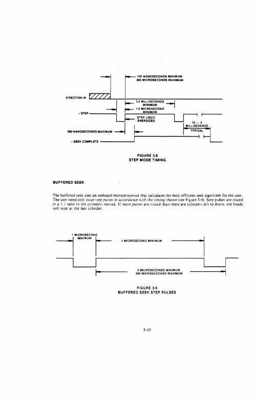
l r 100 NANOSECONDS MINIMUM, 200 MICROSECONDS MAXIMUM
DIRECTION IN ",t<:;.../,-"",Z~/"-",,,.A,--;--;-_-:-:====::--_;--______ _
~ I _ 3.0 MILLISECONDS --J r-- MINIMUM ~ I
_ STEP ------i r-- 1 0 M~~:~SJ~ONO Ll- STEP LOGIC I r--s
ENERGIZED L..J ..
SOONANOSECONDSMAXIMUM ~ I--r-----------~~
- ,SEEK COMPLETE -------'
BUFFERED SEEK
FIGURE 3·8 STEP MODE TIMING
The buffered seek uses an on board microproces .... or that calculates the most efficient seek algorithm for the user. The user need only issue step pulse~ in accordance with the timing "hown (see Figure 3·9). Step pulses are issued in a I: J ratio to the cylinders mmed. If more pulses are issued than there are cylinders left to move, the heads ~oft stop at the lasl cylinder.
--i MI~~N~~t~ONr-- ----1 I I 1 MICROSECOND MINIMUM I
~ ~I --------------~~~~
I s MICROSECONDS MINIMUM. I • 200 MICROSECONDS MAXIMUM •
FIGURE 3·9 BUFFERED SEEK STEP PULSES
3·10
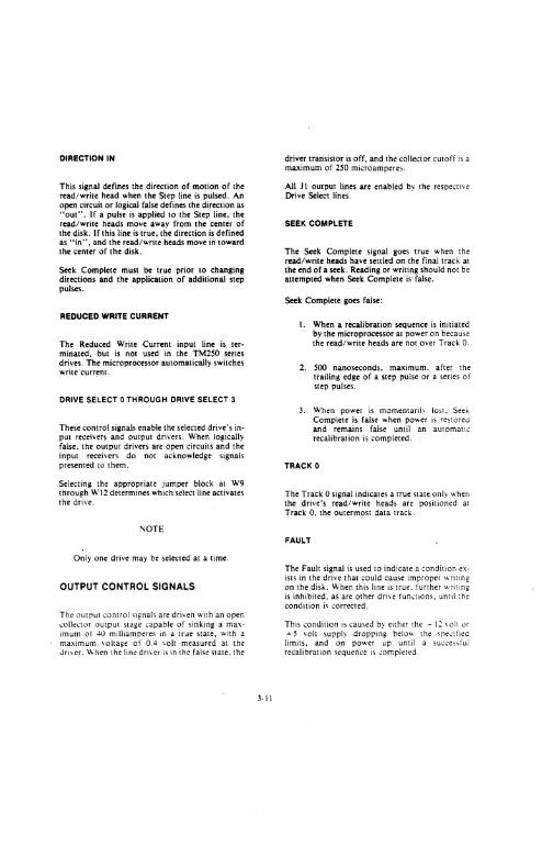
DIRECTION IN
This signal defines the direction of motion of the read/write head when the Step line is pulsed. An open circuit or logical false defines the direction as "out". If a pulse is applied to the Step line. the read/write heads move awav from the center of the disk. If this line is true, the direction is defined as "in" , and the read/write heads move in toward the center of the disk.
Seek Complete must be true prior to changing directions and the application of additional step pulses.
REDUCED WRITE CURRENT
The Reduced Write Current input line is ler~
minaled. but is not used in the TM2S0 series drives. The microprocessor automatically switches write current.
DRIVE SELECT 0 THROUGH DRIVE SELECT 3
These control signals enable the selected drive's in~ PUl receivers and output drivers. When logically false. the output drivers are open circuits and the input receivers do nOt acknowledge signals presented to them.
Selecting the appropriate jumper block at W9 through W12 determines which seieclline activates the drive.
NOTE
Only one drive may be selected at a time.
OUTPUT CONTROL SIGNALS
The output control <;ignals are driven with an open ~ollt:'~lOr output stage I.:apable of sinking a maximum of ... 0 milliamperes in a true state, with a ma:~imum \oltage of 0.4 \,-olt measured at the Jri\er. When the line dnver is in the false stale. the
3-11
driver transistor is off, and the collector cutoff is a maximum of 250 microamperes.
All Jt output lines are enabled by the respecn\.'e Drive Select lines.
SEEK COMPLETE
The Seek Complete signal goes true when the read/write heads have settled on the final track at the end of a seek. Reading or writing should not be attempted when Seek Complete is false.
Seek Complete goes false:
I. When a recalibration sequence is initiated by the microprocessor at power on because the read/write heads are not over Track O.
2. 500 nanoseconds. maximum. after the trailing edge of a step pulse or a series of step pulses.
3. When power is momentaril ... los!. Seek Complete is false when pOYoer is restored and remains false until an automatl'; recalibration is completed.
TRACK 0
The Track 0 signal indicates a true state only when the drive's read/write heads are positioned ar Track 0, the outermost data traCK.
FAULT
The Fault signal is used to indicate a condiuon exists in the drive that could cause improper v. rlung on the disk. When thi':> line is true. fun her writing is inhibited. as are other drive fun.:tlom., untilrhe condition j<; corrected.
This condition is caused by either the - 12 \ 011 or .... 5 vall supply dropping belo\\, the spel,.':ficd limits, and on power up until J sU(:.:e..,~luj recalibration sequence is .;ampleled.
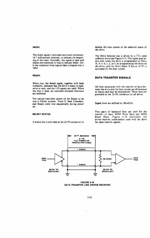
INDEX
The Index signal is provided once each revolution. 16.7 milliseconds nominal, to indicate the beginning of the tracl"" Normally. this signal is false and makes (he transition to true to indicate Index. Only the transition from logical false to logical true is valid.
READY
When true, the Ready signal, together with Seek Complete, indicates that the drive is ready to read, write or seek. and the 1/0 signals are valid. When this line is false. aU controller-initiated functions are inhibited.
The typical time' afler power on for Ready to be true is fifteen seconds. Track 0, Seek Complete, and Ready come true sequentially during power on.
SELECT STATUS
A StalUs line is provided al the J2/P2 connector to
inform the host system of the selection status of the drive.
The Drive Selected line is driven by a TTL open collector drive (see Figure 3-7). This signal goes ac~ tive only when the drive is programmed as Drive X. X = O. 1,2. or 3, by programming the shunt on the drive, and the Drive Select X line al Jl/PI is activated by the host system.
DATA TRANSFER SIGNALS
All lines associated with the transfer of data between the drive and the host system are differential in nature and mav be multiplexed. These lines are provided at the J2/P2 connector on all drives.
Signal level are defined by RS'422A.
Two pairs of balanced lines are used for the transfer of data: MFM Write Data and MFM Read Data. Figure 3-10 illustrates the driver/receiver combination used with the drive for data transfer signals.
r 20 FT. MAXIMUM l (6.1 M)
FlAT RIBBON OR TWISTED PA.R CABLE
HIGH TRUE
26LS310R EQUIVALENT
+ SIGNAL
- SIGNAL
FIGURE 3--10
26LS32 OR EOUIVAL.ENT
DATA TRANSFER LINE DRIVER RECEIVER
3-12
HIGH TRUE
MFM WRITE DATA
This is a differential pair of lines that define the flux transition to be written on the track. The transition of the + MFM Write Data line going more positive than the - MFM Write Data line causes a flux reversal on the track if Write Gate is active. This signa] must be driven 10 an inactive state. T MFM Write Data morc negative than - MFM Write Data, by the host system when in a read mode.
The delay from the leading edge of Write Oate to the Write Data pulse is 400 nanoseconds. maximum.
Host controllers may implement write precompensation circuits that recognize worst case patterns and adjust the write data waveform. Although a value cannot be specified for write precompens8tion. Tandon suggests a value of 12 nanoseconds for systems using MFM double density recording format.
MFM READ DATA
The data recovered by reading a prerecorded track is transmitted to the host system via the differential pair of MFM Read Data lines. The transition of the ... MFM Read Data line going more positive than the -MFM Read Data line represents a flux reversal on the track of the selected head.
3.6 DRIVE ADDRESS AND OPTION SELECTION
The drive address and option selection is determined by the programmable jumper blocks located on the logic circuit board. If jumper con-
3·13
figurations are changed, power should be cycled off and on. so that the microprocessor can recognize the new configuration.
The option programming guide is contained in Table 3·3.
3.7 SHIPPING PACK AND HANDLING
Figures 3·11 through 3·13 provide basic informa· tion on recommended design guidelines for packaging systems.
From various drop tests conducted, it has been established that drives subjected to shock loads in excess of twenty G's may be damaged and consequently not meet published performance specifications for data reliability, margins. and function.
In order to avoid media or head damage. it is recommended that:
1. Drive mounting designs incorporate some type of shock dampening consideration.
2. Shipping cartons protect the drive within the system to withstand twenty G's.
3. Individual drives are handled carefully, e.g .• receiving and in-process personnel are property trained, surface mats are used on working surfaces to prevent the possibility of "handling shock." and padding is placed on racks and carts.
Please emphasize the critical aspects of handling these drives to aU concerned people. In addition. Tandon provides technical assistance on packing and handling to customers upon request.
I TABLE 3·3 OPTION PROGRAMMING GUIDE
I
Factol1 Oplion
Function Proarammed. Usage Jumper Not User Accessible
WI Track Faull 0 Install for excess track fault.
W2 Test 0 Install for unit self-test.
W3 Disable Limit 0 Install to disable soft limits.
W4 Spin Select 0 Install for spin select.
W< Tracks 0 Not used.
WI3 Future Option 0 Install for backlash.
WI4 Future Option I Install for no backlash.
Factor)' Option
Function Proli!:rammed • Usage Jumper User Accessible
WI5 Drive Select I Omit \\'15 for drive-to-controller lines, enabled when drive not selected.
Wlb Inde\. I Omit W 16 for index-to-controller line, enabled when drive not selected.
RT\V: Read Terminator I
} lnstall only at the end drive for daisy chain data, Install in all drive~ for radial data.
WTW8 Write Terminator I
54W9 Drive Select 4 0
3WIO Drive Select 3 0 Install one of four plugs only. Plug corresponds to drive address.
2WII Drive Select 2 0
IWI2 Drive Select 1 I
I LT23 Terminator Pack I Install at the end drive only for daisy chain control lines.
NOTES:
o Omil I Install
3·14
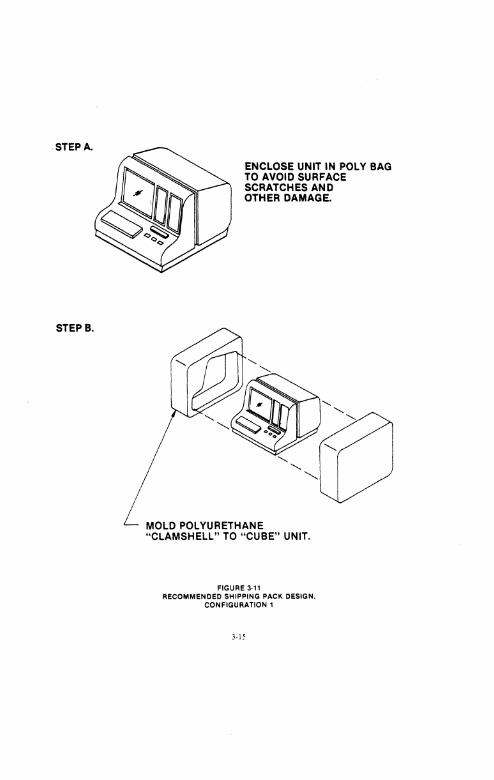
STEPA.
STEP B.
ENCLOSE UNIT IN POLY BAG TO AVOID SURFACE SCRATCHES AND OTHER DAMAGE.
MOLD POLYURETHANE "CLAMSHELL" TO "CUBE" UNIT.
FIGURE 3·" RECOMMENDED SHIPPING PACK DESIGN.
CONFIGURATION'
3· is
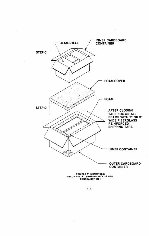
CLAMSHELL INNER CARDBOARD CONTAINER
FOAM COVER
FOAM
AFTER CLOSING, TAPE BOX ON ALL SEAMS WITH 2" OR 3" WIDE FIBERGLASS REINFORCED SHIPPING TAPE.
INNER CONTAINER
OUTER CARDBOARD CONTAINER
FIGURE 3·" (CONTINUED) RECOMMENDED SHIPPING PACK DESIGN.
CONFIGURATION'
3·16
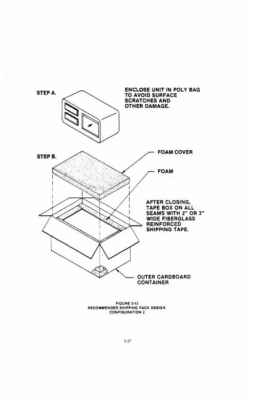
STEPA.
STEPB.
ENCLOSE UNIT IN POLY BAG TO AVOID SURFACE SCRATCHES AND OTHER DAMAGE.
FOAM COVER
FOAM
AFTER CLOSING, TAPE BOX ON ALL SEAMS WITH 2" OR 3" WIDE FIBERGLASS REINFORCED SHIPPING TAPE.
OUTER CARDBOARD CONTAINER
FIGURE 3-12 RECOMMENDED SHIPPING PACK DESIGN.
CONFIGURATION 2
3·17
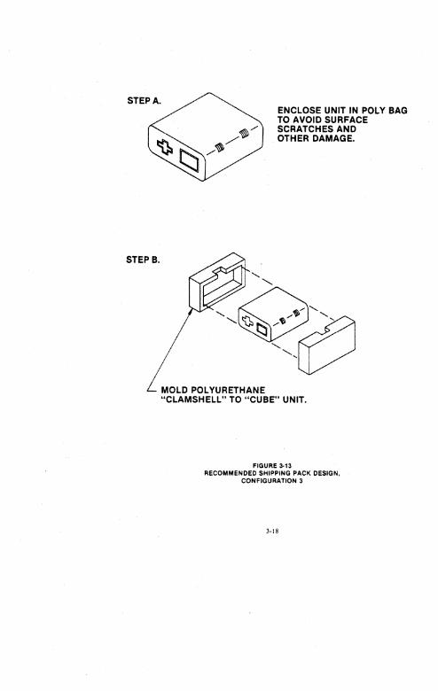
STEP B.
ENCLOSE UNIT IN POLY BAG TO AVOID SURFACE SCRATCHES AND OTHER DAMAGE.
MOLD POLYURETHANE "CLAMSHELL" TO "CUBE" UNIT.
FIGURE 3·13 RECOMMENDED SHIPPING PACK DESIGN,
CONFIGURATION 3
3·18
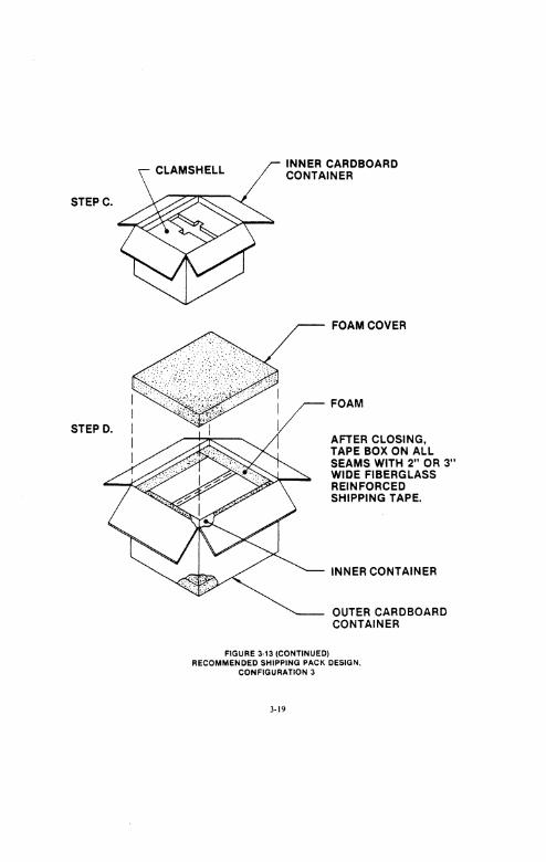
STEPC.
CLAMSHELL INNER CARDBOARD CONTAINER
FOAM COVER
FOAM
AFTER CLOSING, TAPE BOX ON ALL SEAMS WITH 2" OR 3" WIDE FIBERGLASS REINFORCED SHIPPING TAPE.
INNER CONTAINER
OUTER CARDBOARD CONTAINER
FIGURE 3·13 (CONTINUED) RECOMMENDED SHIPPING PACK DESIGN,
CONFIGURATION 3
3·19
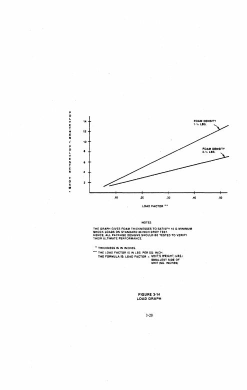
p o L y £ T H £
• I p o L y £ S T £
• F o A M
,. 12
10
.10 .20 .30
LOAD FACTOR""
NOTES
THE GRAPH GIVES FOAM THICKNESSES TO SATISFY 10 G MINIMUM SHOCK LOADS ON SlANDARD 3D·INCH DROP TEST. HENCE, ALL PACKAGE DESIGNS SHOULD BE TESTED TO VERIFY THEIR ULTIMATE PERFORMANCE .
.. THICKNESS IS IN INCHES .
... THE LOAD FACTOR IS IN LBS. PER SO. INCH. THE FORMULA IS: L.OAD FACTOR .. U~[T_~_~_ WEIG._H~_ ilBSJ
SMALLEST SIDE OFUNIT (SO. INCHES)
FIGURE 3·14 LOAD GRAPH
3·20
FOAM DENSITY ,·'1. LSS.
.40 .50

landon CORPORAl E OFFICES 20320 PRAIRIE STREET CHATSWORTH. CA 91311
TEL. NO.: (213) 993-6644 TELEX NO.: 194794 TWX NO.: 910·494·1721
PIN '79050.(I()'" (T5008A ~) PANTED IN U.S.A.
GLOSSARY
2732 EPROM. (Erasable programmable read-only memory). The 2732 EPROM contains the necessary information for the X-Bus master to boot from the hard disk drive.
6331-1 PROM. Programmable read-only memory. The 6331-1 PROM contains information that controls access to the RAM data buffer.
8253 programmable interval timer. The 8253 is a three-channel programmable counter/timer chip manufactured by Intel. Two 8253s are used in the Floppy/Hard Disk Module for interrupt control and DMA transfers. See the Intel Microprocessor and Peripheral Handbook.
Active X-Bus module. An active X-Bus module is a module that, having become the system bus master, can drive all commands and address signals of the X-Bus.
Buffer. A buffer is an amplifying signal driver, not necessarily with memory capability. Buffers that provide temporary storage for data are called "storage buffers."
Bus. A bus is a signal line or a set of lines used by an interface system to connect a number of devices and to transfer information. In general, three types of buses make up a bus set (which is also referred to as a bus): the address bus, the data bus, and the control bus. Also see X-Bus.
Bus cycle. A bus cycle is the process whereby digital signals effect the transfer of data bytes or words across the interface by means of an interlocked sequence of control signals. Interlocked denotes a fixed sequence of events in which one event must occur before the next event can occur.
Bus master. See Master.
Byte. A byte is a group of eight adjacent bits operated on as a unit. Also see High-order byte and Low-order byte.
Clock cycle. A clock cycle is a signal wave form used to achieve synchronization of the timing of switching circuits and memory.
Glossary-l
Cluster configuration. A cluster is a hardware configuration in which cluster workstations are linked in a daisy chain to a master workstation.
Compatibility. Compatibility is the degree to which modules can be interconnected and used without modification.
Direct memory access logic. See DMA.
DHA. (Direct memory access) DMA allows a peripheral device to transfer data to or from memory without using the CPU via a DMA controller in the Processor Module.
DMA address. When the DMA channel is initialized for a transfer, the DMA address is the initial address in memory of the transfer. If the DMA address is read for status· at any time, it is the current memory address of the transfer.
Driver. See Buffer.
Flip-flop. A flip-flop is a digital circuit that can be in either of two states, depending upon the input received and which state it was in when the input was received.
Handshake A handshake is a process whereby control signals are exchanged between the CPU and a device or devices.
High-order byte. The high-oeder byte is the most significant byte in a word (bits Bh to Fh). The high-order byte is also called the odd byte, since it always has an odd address in memory.
High state. The high state is the more positive voltage level used to represent one of two logical binary states (using positive logic).
Identification polling sequence. The identification polling sequence is a .routine in the bootstrap ROM used to identify modules connected to the X-Bus.
Input/output pins. of a chip through output.
Input/output pins are the pins which signals are input or
Interface. An interface is a shared boundary between two systems, or between parts of two systems, through which information is conveyed.
Glossary-2 Floppy/Hard Disk Manual
Interrupt logic. Interrupt logic interrupts the CPU so it can service an I/O or peripheral device.
Local address bus. A local address bus is an address bus that is local to the Floppy/Hard D~sk Module.
Low-order byte. The low-order byte is the least significant byte in a word (bits 0h to 7h). The low-order byte is also called the even byte since is always has an even address in memory.
Low state. The low state is the more negative voltage level used to represent one of two binary states (using positive logic).
Manual reset. A manual reset is a system reset brought about when the user presses the reset button on the rear of the Processor Module. Also see Reset.
Master. In the master-slave concept, the master is a module that controls the data and ad'lress buses. The master acquires the bus (or X-Bus) through bus exchange logic, and then generates command signals, address Signals, and memory or I/O addresses.
Master workstation. The master workstation runs applications and provides resources to individual cluster workstations.
MFM. See Modified frequency modulation.
Modified frequency modulation (MPH). MFM encoding scheme used in the Floppy/Hard Module to store double-density data.
is an Disk
Motherboard. The motherboard interfaces to all boards and power supplies.
NMI. See Nonmaskable interrupt.
Nonmaskable interrupt (NMI). During the X-Bus module identification polling sequence, a nonmaskable interrupt signals a ready timeout to s~gnify that no additional modules are connected to the X-Bus.
PAL. See Programmable array logic.
Passive X-Bus module. A passive X-Bus module is a module that cannot become the X-bus master because
Glossary-3
it is not able to drive the bus command signals of the X-Bus.
Peripheral device. An electromechanical unit. such as a keyboard. CRT. disk drive. or printer that can be connected to the workstation.
Port. A port is an input/output address. usually containing (if a status port) or requiring (if a command port) specific data. such as the Floppy Disk Drive Command/Status register at port XX00h (where XX signi fies the module base I/O address). A port can allow access to several registers. See Register.
Power-up reset. A power-up reset is an automatic system reset occurring when the power is turned on. Also see Reset.
Programmable array logic (PAL). Two l6L8 PAL chips generate control signals for the floppy and hard disk drives.
RAM (Random access memory.) The RAM in the Floppy/Hard Disk Module is made up of four blocks of 2K by 8 bits (2K bytes) of static RAM. totaling 8K bytes.
RAM data buffer. See RAM.
Register. A register is a temporary memory location for data.
Reset. A reset can be either a system reset. as defined by the reset pin functions of the various chips connected to the system reset function. or a software register reset, equivalent to a clear. Also see Power-up reset and Manual reset.
Set. To set is to write a logical 1 or series of l's to a register.
Signal. A signal is the physical representation of logic.
Signal level. The signal level magnitude of a signal when arbitrary reference.
is the relative compared to an
Signal line. A signal line is one of a set of signal conductors in an interface system used to transfer messages among interconnected modules.
Glossary-4 Floppy/Hard Disk Manual
Signal parameters. Signal parameters are the element of an electrical quantity whose values or sequence of values convey information.
State sequencer. Floppy/Hard Disk operations between Bus master.
State sequencer circuitry in the Module controls DMA transfer the RAM data buffer and the X-
Storage buffer. A storage buffer is a buffer with storage, such as a flip-flop, latch, or register.
System. A system is a set of interconnected elements that achieve a given objective through the performance of a specified function.
Tristate buffers. A tristate buffer is a buffer that has these logic output states: ~, 1, and the high impedance state.
Wait state. A wait state is a sion of an I/O or memory cycle. an I/O or memory device operates than that of the CPU.
temporary sus penIt is used when
at a speed slower
WD11!J11!J. The Western Digital WDl01~ Winchester disk controller controls hard disk drive circuitry. See the Western Digital Corp. WDHlle Winchester ~ Controller data sheet.
WD2797-82. The Western Digital WD2797-02 floppy disk formatter/controller contains most of the circuitry necessary in the Floppy/Hard Disk Module to control the floppy disk drive. See the Western Digital Corp. WD279X-02 Floppy Disk Formatter/Controller Family data sheet.
Word. A word is 16 bits or two bytes.
Workstation master. master module within Master.
A workstation master is a a workstation. Also, see
X-Bus. X-Bus is a standard asynchronous system bus that allows for total configurability and interconnection of the workstation modules. The X-Bus supports two independent address spaces: memory and I/O. The X-Bus structure is built upon the master-slave concept, thereby allowing modules of different speeds to interface.
X-Bus master. Module that controls the X-Bus.
Glossary-5
INDEX
1-of-8 decoder, 3-45, 3-47, 3-70 16L8 PAL programs, 2-43 4K-byte EPROM, 3-52 6331-1 PROM, 1-4
control of chip selects by, 3-52 firmware routine, 3-54
8253 Mode Control word, 2-18, 2-33, 2-36 8253 programmable interval timer, 1-4,
2-19, 3-20, 3-38, 3-47, 3-58, 3-70 circuit, 2-8, 2-9 hard disk control, 2-34, 2-37 internal registers of, 3-74, 3-79 pin assignments and functions,
3-72 to 3-73 Addressable devices, 3-20
8253 programmable interval timers, 3-20
WD1010, 3-20 WD2797-02, 3-20
Address mark, 2-26 Architecture, 2-1 to 2-47
Base I/O address, 2-5, 2-44 assigned by Processor Module, 2-44 assigning, 3-17 changing, 2-44 to 2-45 written by Processor Module to Floppy
Hard Disk Module, 3-17, 3-19 written for the Floppy Hard Disk
Module, 3-19 Binary coded decimal, 2-19 Bootstrap ROM, 2-2, 2-5 to 2-6 Buffer data request flag, 2-24 Burst size, 3-58
Circuit descriptions, 3-1 Command register, 2-9, 2-24, 2 30
command byte written into, 3-35 floppy disk drive, 2-9 hard disk controller,2-24, 2-30
Command register commands for hard disk drive, 2-30
Read Sector, 2-30 Restore, 2-30 Scan 10, 2-30 Seek, 2-30 Write Format, 2-30 Write Sector, 2-30
Index-l
Command register functio:.!' ~" .... hard disK drive, 2-30
direct memory access, 2-30, multiple sector read or write, 2-30, programmed I/O, 2-30, single sector read or write, 2-30,
Control register functions for hard disk drive, 2-31
8253 mode control, 2-31, Hard DisK Drive Control register, 2-31 X-Bus Extended Address register, 2-31
Control registers for hard disk dr~ve, 2-31
Control signals, 3-37 for hard disk drive, 3-48 from Floppy Disk Drive Control
register, 3-38 from WD2797-02, 3-37 generation of, 2~42
Control signal functions for floppy disk drive, 3-37, 3-38, 3-48
Drive Motor On, 3-38 Drive Select 0, 3-38, 3-48 Drive Select 1, 3-48 Head Select 0/Expansion HS0, 3-48 Head Select l/Expansion HSl, 3~48 Head Select 2/Expansion HS2, 3-48 Multiplex, 3-38 Side Select, 3-38 Step Direction, 3-37 Step Pulse, 3-37 Write Data, 3-37 Write Gate, 3-37
Conventions, xix Counter 0, 2-8, 2-18, 2-35
Mode Control word for, 2-37 Counter 1, 2-8
Mode Control word for, 2-37 Counter 2, Mode Control word for, 2-34,
2-37 CRC. automatic generation of, 2-39 CRe bytes,
computing in event of read error, 3-70 computing of, 3-74
CRC generator, 2-20 Cyclic redundancy checking (CRC)
circuitry, 1-4 Cylinder number, 2-27 Cylinder Number High register, 2-28 Cylinder Number Low register, 2-28
Data register, 2-2, 2-7, 2-8, 2-16, 2-20 serial byte loaded into, 3-35
Data Request line, 2-20
Indellt-2 Floppy/Hard Disk Manual
Data Shift register, 2-20 Data transceivers, 3-18 Dc/dc power converters in Floppy Hard
Disk Module, 1-5, 3-80 Direct memory access transfers, 3-58 to
3-62 Disable read/write, 3-46 DMA burst, 2-35, 2-36, 3-47, 3-64 DMA burst count, 3-79 DMA cycle
during, 3-52 indication of its being in progress,
3-20, 3-22 indication of its not being in
progress, 3-36 start of, 3-63
DMA delay count, 3-79 DMA transfer, 2-33, 3-64, 3-65, 3-79
word counts, 3-58 Double-density storage, 1-3 Double-sided media, 1-3
Error register, 2-26
Floppy disk, 1-3 to 1-4 formatting, 2-20 to 2-23 operation, 3-70 sectors, 2-23 track format, 2-21 to 2-22 values, 2-23
Floppy disk circuitry, 1-4 Floppy disk control, 2-19 Floppy disk control logic, major
components, 1-5 programmable interval timer, 1-5 WD2797-02 floppy disk
formatter/controller, 1-5 Floppy disk controller, 2-7 to 2-8 Floppy disk controller commands
Force Interrupt, 2-10 Read Address, 2-10 Read Sector, 2-10 Read Track, 2-10 Restore, 2-10 Seek, 2-10 Step, 2-10 Step-In, 2-10 Step-Out, 2-10 Write Sector, 2-10 Write Track, 2-10
Floppy disk controller command summary, 2-10
Index-3
Floppy disk controller data interface, 3-21
Floppy disk controller flag summary, 2-11 to 2-12
data address mark, 2-12 head load flag, 2-11 interrupt condition flags, 2-12 multiple record flag, 2-11 sector length flag, 2-11 stepping motor rate, 2-11 track number verify flag, 2-11 track upoate flag, 2-11 update SSO, 2-12
Floppy disk controller logic, functional block diagram, 3-33 to 3-34
Floppy disk drive controller logic, 3-27, 3-33 to 3-34 formatting a track on, 2-20 interface logic, 3-36 light, enabling of, 3-38 motor, 3-38 read or write operations to by X-Bus
master, 3-35 Floppy disk drive clock logic, 3-36 Floppy disk drive control and status
registers, 2-9 Floppy Disk Drive Control register, 2-9,
2-17, 2-36 clocking of, 3-26
Floppy/hard disk interconnect wire list, 3-81 to 3-85
Floppy/Hard Disk Module Controller board, 1-5 dc/dc power converters, 1-5, 3-80 device decoding, 3-24 enclosure, 1-5 general description, 1-3 to 1-4 half-height floppy disk drive, 1-5 half-height hard disk drive, 1-5 hardware, 2-1 I/O ports, 2-2 major components, 1-5 motherboard, 1-5 PAL chips used in, 2-42 power requirements, A-I schematic diagram, 3-3 to 3-15 specification, A-I X-Bus interface, 1-5
Force Interrupt command, 2-8, 3-70 issued by X-Bus master, 3-74
Formatting operation, data for, 2-20 Functional h10ck diagrams
floppy disk drive controller logic, 3-33 to 3-34
Index-4 Floppy/Hard Disk Manual
Functional block diagrams (cont.) hard disk drive controller logie,
3-41, to 3-42 programmable interval timer logic,
3-7~ to 71 Functional Logic block diagram,
Floppy/Hard Disk Module, 2-3 to 2-4
Hard disk, 1-4 Hard disk circuitry, 1-4 Hard disk controller, 3-75
data interface, 3-21 logic, 3-4~
8253 programmable interval timers, 1-5
major components, 1-5 WD1~1~ Winchester disk controller,
1-5 task information, 2-24
disk cylinder number, 2-24 drive number, 2-24 head number, 2-24 sector number,2-24 sector size. 2-24 track number for start of write
precompensation, 2-24 Hard disk controller logic. functional
block diagram. 3-41 to 42 Hard disk drive
Boot ROM. 3-52 clock logic. 3-47 command and status registers. 2-25 to
2-38 controller RAM data buffer. 3-52 interface logic. 3-47 MFM clock and data pulses driven to.
3-69 read/write circuitry. 3-66
Hard Disk Drive Control register. 2-32. 3-47. 3-49
clocking of. 3-26 functions. 2-32 WD1~1~ reset, 2-32
Hard disk expansion. 3-86 Hard disk expansion interconnect wire
list. 3-87 to 3-9~ Hard Disk Expansion Module, 1-2 Hard disk formatting, 2-39 to 2-41 Hard disk track format. 2-41 Hard-wired buffers. 3-18 Head position, 2-16 High-order data lines. assignment of.
3-18
Index-5
I/O address, issued by Processor Module, 3-19
I/O Address register, 3-19, 3-20 I/O address summary associated logic,
2-46 floppy disk 8253, 2-46 floppy disk drive, 2-46 hard disk 8253, 2-47 hard disk drive, 2-46 WDHH0, 2-47 WD2797-02, 2-46 X-Bus addressing, 2-46
I/O ports, base addresses for, 3-17 I/O reads or writes, 3-20 Identification polling sequence, 3-19 Identifier buffers, disabling of, 3-20 Identifier for Floppy/Hard Disk Module,
3-19 Identifier number, 3-18 Identifying code, 3-18 Index mark, 2-20 Index pulse, 2-20, 2-26, 2-39 Input signals, 3-18 Integrated circuit l3E, 2-43 Integrated circuit 7E, 2-43 Integration circuit (IC) designations,
2-43 Interface, between WD2797-02 formatter
controller and floppy disk drive, 3-36
Interleave factor, 2-39 Interrupt function, 3-74
Keyboard, 1-1
Load counter 0, 2-9 Load counter 1, 2-9 Local module data bus interface, 3-21 Log1cal sector number, 2-39 Low-order data lines, 3-19
Major components of Floppy/Hard Disk Module, 1-5
Memory address data, during a DMA cycle, 3-22
Memory table, module identifier stored in, 3-19
MFM, CRC characters generated in, 2-20 MFM data, 3-66,3-67, 3-68
phase-locked loop clocked to, 3-68 Mode Control register, 2-37 Modified Frequency Modulation (MFM), 1-3
Index-6 Floppy/Bard Disk Manual
Module base I/O address, 3-20 summary, 2-44
Module I/O address summary, 2-46, 2-47 Module identification, 2-2
implementation, 2-5 Module identifier, 3-19 Monitor, 1-1 Multiple-sector read, 2-8
Nonmaskable interrupt (NMI), 2-2
OEM manuals, 1-2, B-1, C-l Operating system, changing the module
address through, 2-2
Panel Debugger routine, using to change base I/O address, 2-44
Phase synchronization, 3-68 Phase-comparison flip-flop, 3-67, 3-68 Phase-comparison window, 3-67, 3-68 Phase-detection circuitry, 3-67 Phase-detector enable flip-flop, 3-67,
3-68 Phase-frequency detector, inputs of,
3-67 Phase-locked loop, 3-47
circuitry, 3-68 data separator, 1-4 data separator circuitry, 1-4
Pin assignments and functions, WD2797-02 FD formatter/controller, 3-28 to 3-32
Power supplies, 3-80 Power up, 2-5, 2-44 Precompensation, 2-27 Processor Module, 1-1, 2-5
base I/O address isssued by, 2-2 bootstrap ROM program in, 2-2 communication with Floppy Hard Disk
Module, 3-17 Programmable array logic (PAL), 1-4,
2-39 to 2-43 Pump down, 3-67, 3-68 Push-button reset, 2-44
Race condition, 3-74 RAM chip addressing, 3-55 RAM chip selection, 3-55
Index-7
RAM data buffers, 1-4, 2-14, 3-46, 3-57 loading, 3-68 map, 3-53 memory of, 3-52 read from or written to by WD1919,
3-55 RAM data direction, 3-57 RAM data lines, 3-57 Read operations, 3-35, 3-74, 3-79 Read/write operation, 2-16 Reduced write current (RWC), 2-27 Registers
Command, 2-9, 2-24, 2-39, 2-35 Cylinder Number High, 2-28 Cylinder Number Low, 2-28 Data, 2-2, 2-7, 2-8, 2-16, 2-29 Data Shift, 2-29 Error, 2-26, Floppy DisK Drive Control, ~-9, 2-17,
2-36 Hard DisK Drive Control,2-32, 3-47,
3-49 I/O Address, 3-19, 3-29 Mode Control, 2-37 Sector, 2-7, 2-9, 2-16 Sector Count, 2-27, 2-39 Sector/Drive/Head, 2-28, 2-39 Sector Number, 2-27, 2-39 Status, 2-7, 2-9, 2-29 TasK, 3-46 Task File, 2-25, 2-39 Track, 2-7, 2-9, 2-16 WD191121 Command, 3-5121 WD2797-1212
Data, 2-18 Data Shift, 2-16 Status, 2-16
Write Precompensation Cylinder, 2-27 X-Bus Extended Address, 3-46
Registers, base addresses for, 3-17 Reset, manual, 2-2 Reset, power-up, 2-2 RS-422 receiver, 3-66
Sample sector buffer, 2-4121 Sector buffer, 2-39 Sector Count register, 2-27, 2-39 Sector/Drive/Head register, 2-28, 2-39 Sector/Drive/Head register functions,
2-28 drive number, 2-28 head number, 2-28 sector extension, 2-28 sector size, 2-28
Index-8 Floppy/Bard Disk Manual
Sector number, 2-16 Sector Number register, 2-27, 2-39 Sector position, 2-16 Sector register, 2-7, 2-9, 2-16 Sector's ID field, bad block mark
recorded in, 2-39 Seek command, 2-16 Seek operation, 2-16, 3-38 Seeks, track, 3-27 Software debugger, 2-45
using to change base I/O address, 2-45 State machine, 3-55
outputs of, 3-64 State sequencer, 3-63
circuitry, for DMA transfer operations, 3-63
timing, 3-63 Status register commands, 2-13
Busy, 2-13 eRC Error, 2-13 Head Loaded, 2-13 Index Pulse, 2-13 Not Ready, 2-13 Seek Error. 2-13 Track 00, 2-13 Write Protect, 2-13
Status register for floppy disk drive, 2-7, 2-9, 2-29
Status register for hard disk drive. 2-29
Status register functions for WD1010 Drive Ready, 2-29 Seek Complete, 2-29 use of RAM data buffer in, 2-29 Write Fault, 2-29
Status register summary for floppy disk controller, 2-13 to 2-15
Status signals for WD2797-02, 3-39 functions, 3-39
Drive Ready, 3-39 Floppy Write Protected, 3-39 Index Mark Detected, 3-39 Track 0 Detected, 3-39
Stepping signals (Controls). for WD1010, 3-51
functions, 3-51 STEP1-/STEP2.3-51 DIR1-/DIR2-. 3-51 RWC1-/RWC2-. 3-51 WRGT1-/WRGT2-, 3-51
Stepping signals (Status), for WD1010, 3-50
functions, 3-50 Seek Complete, 3-50 Winchester Drive Ready, 3-50
Index-9
Stepping signals (Status), for WD1010, functions (cont.) Winchester Index Pulse, 3-50 Winchester Track 0, 3-50 Write Fault, 3-50
Task File registers, 2-25, 2-39 Task registers, 3-46 Theory of operation, 3-1 to 3-90 Timing diagrams, 3-59 to 3-61
read/write sector, 3-59 single sector read, 3-60 single sector write, 3-61
Timing of the state sequencer, 3-63 Track register, 2-7, 2-9, 2-16 Transfer acknowledge generation, 3-24 Tristate buffer, enabling of, 3-22 Type-state word, 2-2, 2-6
Voltage-controlled oscillator (Vea), 3-67
WD1010, 3-45 Command register of, 3-50 data written by, 3-69 formatting of track, 2-39 high signal generated to, 3-66 write or read enabled by, 3-52
WD1010 Winchester disk controller pin assignments and functions, 3-43 to 3-45
Task File registers, 2-24 WD 2797-02, 2-8 to 2-20
Control commands, 2-7 Data register, 2-18 Data Shift register, 2-16 Force Interrupt command. 2-7, 2-8 Read/Write commands, 2-7 Sector' register data written into,
3-35 Status register, 2-16 Track register, data written into,
3-35 WD2797-02 floppy disk
formatter/controller, 3-27 circuitry in. 3-27
address mark generation and detection, 3-27
CRC, 3-27 phase-locked loop data separator.
3-27 write precompensation, 3-27
Index-I" Floppy/Hard Disk Manual
WD2797-02 floppy disk formatter/controller (cont.)
commands, 2-7 enabling of, 3-35 read operation, 3-70
Western Digital WD10l0 Winchester disk controller, 1-4
Wire lists, 3-81 to 3-85, 3-87 to 3-90 Word count, 3-79 Workstations
cluster, 1-1 master, 1-1 standalone, 1-1
Write operations, 3-35, 3-79 Write precompensation circuitry, i-4,
3-27 Write Precompensation Cylinder register,
2-27 Write Sector command, 2-8, 2-24, 3-46 Write Track command, 2-20
X-Bus, 1-1 address control register, clocking of,
3-26 address lines, decoding of, 3-24 data interface, 3-21 data lines, 2-7, 3-19 Extended Address register, 3-46, 3-62
data bits at, 3-62 use of the WD1010 in, 2-33
identification, 3-17 to 3-20 interface, 2-2 to 2-6, 3-17 manual (push-button) reset on, 3-17 module identification, 2-2 modules, 2-5 modules 00, 2-44 to reset, 2-45
X-Bus master, 1-1, 1-3, 2-7, 2-8, 2-18, 3-45, 3-46, 3-47
accessing by, 3-52 command loaded by, 3-79 DMA request to, 3-62 in termination of search, 3-70 interruption when command completed,
3-36 interrupt to, 2-9 I/O read cycle, 3-21 I/O write cycle, 3-21 memory, 2-20
interrupt to asserted, 2-20 response, 3-62 selection of registers by, 3-35 task information written by, 2-24 words transferred to, 3-58
Index-ll

Floppy/Hard Disk Manual
First Edition January 1984 A-09-00328-01-A