Embed Size (px)
Citation preview
TL/F/9419
Flo
ppy
Dis
kD
ata
Separa
torD
esig
nG
uid
efo
rth
eD
P8473
AN
-505
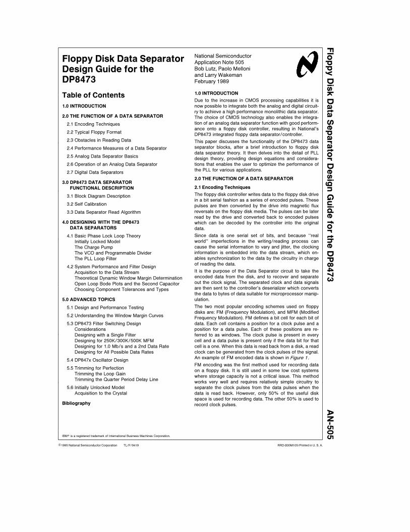
National SemiconductorApplication Note 505Bob Lutz, Paolo Melloniand Larry WakemanFebruary 1989
Floppy Disk Data SeparatorDesign Guide for theDP8473
Table of Contents
1.0 INTRODUCTION
2.0 THE FUNCTION OF A DATA SEPARATOR
2.1 Encoding Techniques
2.2 Typical Floppy Format
2.3 Obstacles in Reading Data
2.4 Performance Measures of a Data Separator
2.5 Analog Data Separator Basics
2.6 Operation of an Analog Data Separator
2.7 Digital Data Separators
3.0 DP8473 DATA SEPARATOR
FUNCTIONAL DESCRIPTION
3.1 Block Diagram Description
3.2 Self Calibration
3.3 Data Separator Read Algorithm
4.0 DESIGNING WITH THE DP8473
DATA SEPARATORS
4.1 Basic Phase Lock Loop Theory
Initially Locked Model
The Charge Pump
The VCO and Programmable Divider
The PLL Loop Filter
4.2 System Performance and Filter Design
Acquisition to the Data Stream
Theoretical Dynamic Window Margin Determination
Open Loop Bode Plots and the Second Capacitor
Choosing Component Tolerances and Types
5.0 ADVANCED TOPICS
5.1 Design and Performance Testing
5.2 Understanding the Window Margin Curves
5.3 DP8473 Filter Switching Design
Considerations
Designing with a Single Filter
Designing for 250K/300K/500K MFM
Designing for 1.0 Mb/s and a 2nd Data Rate
Designing for All Possible Data Rates
5.4 DP847x Oscillator Design
5.5 Trimming for Perfection
Trimming the Loop Gain
Trimming the Quarter Period Delay Line
5.6 Initially Unlocked Model
Acquisition to the Crystal
Bibliography
1.0 INTRODUCTION
Due to the increase in CMOS processing capabilities it is
now possible to integrate both the analog and digital circuit-
ry to achieve a high performance monolithic data separator.
The choice of CMOS technology also enables the integra-
tion of an analog data separator function with good perform-
ance onto a floppy disk controller, resulting in National’s
DP8473 integrated floppy data separator/controller.
This paper discusses the functionality of the DP8473 data
separator blocks, after a brief introduction to floppy disk
data separator theory. It then delves into the detail of PLL
design theory, providing design equations and considera-
tions that enables the user to optimize the performance of
the PLL for various applications.
2.0 THE FUNCTION OF A DATA SEPARATOR
2.1 Encoding Techniques
The floppy disk controller writes data to the floppy disk drive
in a bit serial fashion as a series of encoded pulses. These
pulses are then converted by the drive into magnetic flux
reversals on the floppy disk media. The pulses can be later
read by the drive and converted back to encoded pulses
which can be decoded by the controller into the original
data.
Since data is one serial set of bits, and because ‘‘real
world’’ imperfections in the writing/reading process can
cause the serial information to vary and jitter, the clocking
information is embedded into the data stream, which en-
ables synchronization to the data by the circuitry in charge
of reading the data.
It is the purpose of the Data Separator circuit to take the
encoded data from the disk, and to recover and separate
out the clock signal. The separated clock and data signals
are then sent to the controller’s deserializer which converts
the data to bytes of data suitable for microprocessor manip-
ulation.
The two most popular encoding schemes used on floppy
disks are: FM (Frequency Modulation), and MFM (Modified
Frequency Modulation). FM defines a bit cell for each bit of
data. Each cell contains a position for a clock pulse and a
position for a data pulse. Each of these positions are re-
ferred to as windows. The clock pulse is present in every
cell and a data pulse is present only if the data bit for that
cell is a one. When this data is read back from a disk, a read
clock can be generated from the clock pulses of the signal.
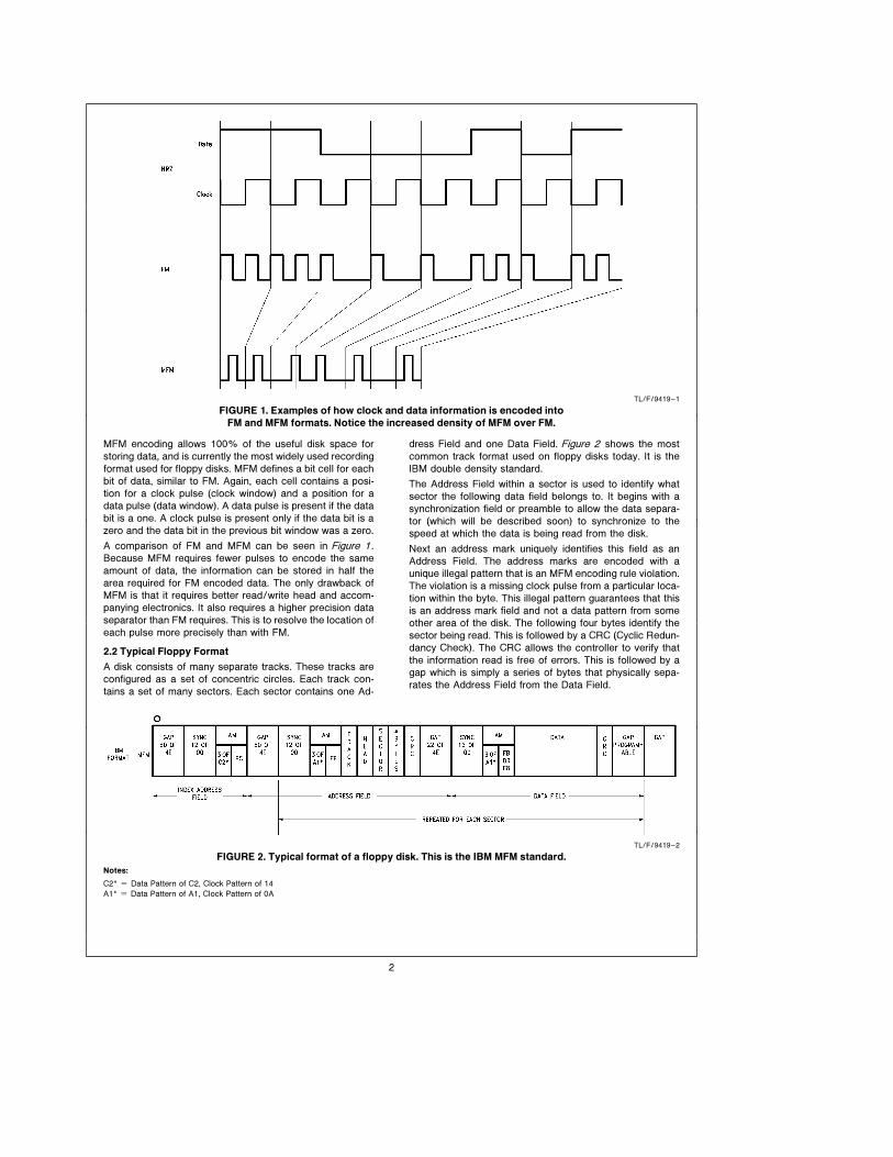
An example of FM encoded data is shown in Figure 1.
FM encoding was the first method used for recording data
on a floppy disk. It is still used in some low cost systems
where storage capacity is not a critical issue. This method
works very well and requires relatively simple circuitry to
separate the clock pulses from the data pulses when the
data is read back. However, only 50% of the useful disk
space is used for recording data. The other 50% is used to
record clock pulses.
IBMÉ is a registered trademark of International Business Machines Corporation.
C1995 National Semiconductor Corporation RRD-B30M105/Printed in U. S. A.
TL/F/9419–1
FIGURE 1. Examples of how clock and data information is encoded into
FM and MFM formats. Notice the increased density of MFM over FM.
MFM encoding allows 100% of the useful disk space for
storing data, and is currently the most widely used recording
format used for floppy disks. MFM defines a bit cell for each
bit of data, similar to FM. Again, each cell contains a posi-
tion for a clock pulse (clock window) and a position for a
data pulse (data window). A data pulse is present if the data
bit is a one. A clock pulse is present only if the data bit is a
zero and the data bit in the previous bit window was a zero.
A comparison of FM and MFM can be seen in Figure 1.
Because MFM requires fewer pulses to encode the same
amount of data, the information can be stored in half the
area required for FM encoded data. The only drawback of
MFM is that it requires better read/write head and accom-
panying electronics. It also requires a higher precision data
separator than FM requires. This is to resolve the location of
each pulse more precisely than with FM.
2.2 Typical Floppy Format
A disk consists of many separate tracks. These tracks are
configured as a set of concentric circles. Each track con-
tains a set of many sectors. Each sector contains one Ad-
dress Field and one Data Field. Figure 2 shows the most
common track format used on floppy disks today. It is the
IBM double density standard.
The Address Field within a sector is used to identify what
sector the following data field belongs to. It begins with a
synchronization field or preamble to allow the data separa-
tor (which will be described soon) to synchronize to the
speed at which the data is being read from the disk.
Next an address mark uniquely identifies this field as an
Address Field. The address marks are encoded with a
unique illegal pattern that is an MFM encoding rule violation.
The violation is a missing clock pulse from a particular loca-
tion within the byte. This illegal pattern guarantees that this
is an address mark field and not a data pattern from some
other area of the disk. The following four bytes identify the
sector being read. This is followed by a CRC (Cyclic Redun-
dancy Check). The CRC allows the controller to verify that
the information read is free of errors. This is followed by a
gap which is simply a series of bytes that physically sepa-
rates the Address Field from the Data Field.
TL/F/9419–2
FIGURE 2. Typical format of a floppy disk. This is the IBM MFM standard.
Notes:
C2* e Data Pattern of C2, Clock Pattern of 14
A1* e Data Pattern of A1, Clock Pattern of 0A
2
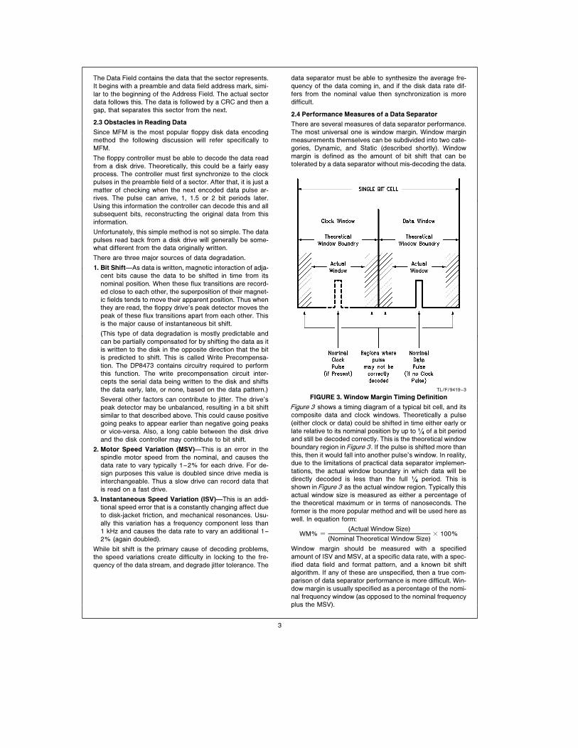
The Data Field contains the data that the sector represents.
It begins with a preamble and data field address mark, simi-
lar to the beginning of the Address Field. The actual sector
data follows this. The data is followed by a CRC and then a
gap, that separates this sector from the next.
2.3 Obstacles in Reading Data
Since MFM is the most popular floppy disk data encoding
method the following discussion will refer specifically to
MFM.
The floppy controller must be able to decode the data read
from a disk drive. Theoretically, this could be a fairly easy
process. The controller must first synchronize to the clock
pulses in the preamble field of a sector. After that, it is just a
matter of checking when the next encoded data pulse ar-
rives. The pulse can arrive, 1, 1.5 or 2 bit periods later.
Using this information the controller can decode this and all
subsequent bits, reconstructing the original data from this
information.
Unfortunately, this simple method is not so simple. The data
pulses read back from a disk drive will generally be some-
what different from the data originally written.
There are three major sources of data degradation.
1. Bit ShiftÐAs data is written, magnetic interaction of adja-
cent bits cause the data to be shifted in time from its
nominal position. When these flux transitions are record-
ed close to each other, the superposition of their magnet-
ic fields tends to move their apparent position. Thus when
they are read, the floppy drive’s peak detector moves the
peak of these flux transitions apart from each other. This
is the major cause of instantaneous bit shift.
(This type of data degradation is mostly predictable and
can be partially compensated for by shifting the data as it
is written to the disk in the opposite direction that the bit
is predicted to shift. This is called Write Precompensa-
tion. The DP8473 contains circuitry required to perform
this function. The write precompensation circuit inter-
cepts the serial data being written to the disk and shifts
the data early, late, or none, based on the data pattern.)
Several other factors can contribute to jitter. The drive’s
peak detector may be unbalanced, resulting in a bit shift
similar to that described above. This could cause positive
going peaks to appear earlier than negative going peaks
or vice-versa. Also, a long cable between the disk drive
and the disk controller may contribute to bit shift.
2. Motor Speed Variation (MSV)ÐThis is an error in the
spindle motor speed from the nominal, and causes the
data rate to vary typically 1–2% for each drive. For de-
sign purposes this value is doubled since drive media is
interchangeable. Thus a slow drive can record data that
is read on a fast drive.
3. Instantaneous Speed Variation (ISV)ÐThis is an addi-
tional speed error that is a constantly changing affect due
to disk-jacket friction, and mechanical resonances. Usu-
ally this variation has a frequency component less than
1 kHz and causes the data rate to vary an additional 1–
2% (again doubled).
While bit shift is the primary cause of decoding problems,
the speed variations create difficulty in locking to the fre-
quency of the data stream, and degrade jitter tolerance. The
data separator must be able to synthesize the average fre-
quency of the data coming in, and if the disk data rate dif-
fers from the nominal value then synchronization is more
difficult.
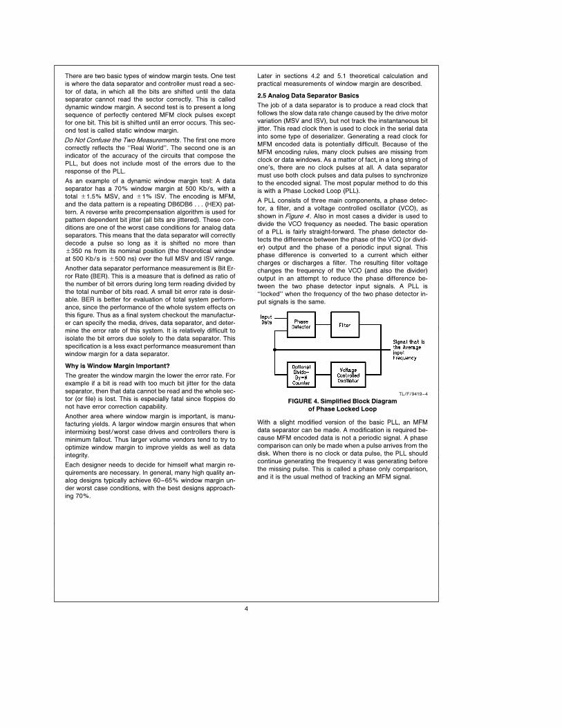
2.4 Performance Measures of a Data Separator
There are several measures of data separator performance.
The most universal one is window margin. Window margin
measurements themselves can be subdivided into two cate-
gories, Dynamic, and Static (described shortly). Window
margin is defined as the amount of bit shift that can be
tolerated by a data separator without mis-decoding the data.
TL/F/9419–3
FIGURE 3. Window Margin Timing Definition
Figure 3 shows a timing diagram of a typical bit cell, and its
composite data and clock windows. Theoretically a pulse
(either clock or data) could be shifted in time either early or
late relative to its nominal position by up to (/4 of a bit period
and still be decoded correctly. This is the theoretical window
boundary region inFigure 3. If the pulse is shifted more than
this, then it would fall into another pulse’s window. In reality,
due to the limitations of practical data separator implemen-
tations, the actual window boundary in which data will be
directly decoded is less than the full (/4 period. This is
shown inFigure 3 as the actual window region. Typically this
actual window size is measured as either a percentage of
the theoretical maximum or in terms of nanoseconds. The
former is the more popular method and will be used here as
well. In equation form:
WM% e
(Actual Window Size)
(Nominal Theoretical Window Size)c 100%
Window margin should be measured with a specified
amount of ISV and MSV, at a specific data rate, with a spec-
ified data field and format pattern, and a known bit shift
algorithm. If any of these are unspecified, then a true com-
parison of data separator performance is more difficult. Win-
dow margin is usually specified as a percentage of the nomi-
nal frequency window (as opposed to the nominal frequency
plus the MSV).
3
There are two basic types of window margin tests. One test
is where the data separator and controller must read a sec-
tor of data, in which all the bits are shifted until the data
separator cannot read the sector correctly. This is called
dynamic window margin. A second test is to present a long
sequence of perfectly centered MFM clock pulses except
for one bit. This bit is shifted until an error occurs. This sec-
ond test is called static window margin.
Do Not Confuse the Two Measurements . The first one more
correctly reflects the ‘‘Real World’’. The second one is an
indicator of the accuracy of the circuits that compose the
PLL, but does not include most of the errors due to the
response of the PLL.
As an example of a dynamic window margin test: A data
separator has a 70% window margin at 500 Kb/s, with a
total g1.5% MSV, and g1% ISV. The encoding is MFM,
and the data pattern is a repeating DB6DB6 . . . (HEX) pat-
tern. A reverse write precompensation algorithm is used for
pattern dependent bit jitter (all bits are jittered). These con-
ditions are one of the worst case conditions for analog data
separators. This means that the data separator will correctly
decode a pulse so long as it is shifted no more thang350 ns from its nominal position (the theoretical window
at 500 Kb/s is g500 ns) over the full MSV and ISV range.
Another data separator performance measurement is Bit Er-
ror Rate (BER). This is a measure that is defined as ratio of
the number of bit errors during long term reading divided by
the total number of bits read. A small bit error rate is desir-
able. BER is better for evaluation of total system perform-
ance, since the performance of the whole system effects on
this figure. Thus as a final system checkout the manufactur-
er can specify the media, drives, data separator, and deter-
mine the error rate of this system. It is relatively difficult to
isolate the bit errors due solely to the data separator. This
specification is a less exact performance measurement than
window margin for a data separator.
Why is Window Margin Important?
The greater the window margin the lower the error rate. For
example if a bit is read with too much bit jitter for the data
separator, then that data cannot be read and the whole sec-
tor (or file) is lost. This is especially fatal since floppies do
not have error correction capability.
Another area where window margin is important, is manu-
facturing yields. A larger window margin ensures that when
intermixing best/worst case drives and controllers there is
minimum fallout. Thus larger volume vendors tend to try to
optimize window margin to improve yields as well as data
integrity.
Each designer needs to decide for himself what margin re-
quirements are necessary. In general, many high quality an-
alog designs typically achieve 60–65% window margin un-
der worst case conditions, with the best designs approach-
ing 70%.
Later in sections 4.2 and 5.1 theoretical calculation and
practical measurements of window margin are described.
2.5 Analog Data Separator Basics
The job of a data separator is to produce a read clock that
follows the slow data rate change caused by the drive motor
variation (MSV and ISV), but not track the instantaneous bit
jitter. This read clock then is used to clock in the serial data
into some type of deserializer. Generating a read clock for
MFM encoded data is potentially difficult. Because of the
MFM encoding rules, many clock pulses are missing from
clock or data windows. As a matter of fact, in a long string of
one’s, there are no clock pulses at all. A data separator
must use both clock pulses and data pulses to synchronize
to the encoded signal. The most popular method to do this
is with a Phase Locked Loop (PLL).
A PLL consists of three main components, a phase detec-
tor, a filter, and a voltage controlled oscillator (VCO), as
shown in Figure 4. Also in most cases a divider is used to
divide the VCO frequency as needed. The basic operation
of a PLL is fairly straight-forward. The phase detector de-
tects the difference between the phase of the VCO (or divid-
er) output and the phase of a periodic input signal. This
phase difference is converted to a current which either
charges or discharges a filter. The resulting filter voltage
changes the frequency of the VCO (and also the divider)
output in an attempt to reduce the phase difference be-
tween the two phase detector input signals. A PLL is
‘‘locked’’ when the frequency of the two phase detector in-
put signals is the same.
TL/F/9419–4
FIGURE 4. Simplified Block Diagram
of Phase Locked Loop
With a slight modified version of the basic PLL, an MFM
data separator can be made. A modification is required be-
cause MFM encoded data is not a periodic signal. A phase
comparison can only be made when a pulse arrives from the
disk. When there is no clock or data pulse, the PLL should
continue generating the frequency it was generating before
the missing pulse. This is called a phase only comparison,
and it is the usual method of tracking an MFM signal.
4
TL/F/9419–5
FIGURE 5. Simplified Block Diagram of Typical Data Separator
A typical data separator is shown in Figure 5. In addition to
the components of a typical PLL, it includes a quarter period
delay line and either a pulse gate or pulse inserter (not
both). Both of these blocks enable the pulse gate or pulse
inserter to decide when the phase comparison should be
made. The quarter period delay line delays the incoming
data pulses a quarter of a bit cell, and this feeds the pulse
gate or pulse inserter. The pulse gate will disable phase
comparisons when a VCO pulse occurs but read data puls-
es are missing. The pulse inserter will insert fake read data
pulses into the phase detector when there is a VCO pulse
but no read data pulse. These components are required to
determine the proper timing of the phase comparisons for
MFM encoded data. The need for these blocks can be dem-
onstrated by referring to Figure 6. Only the use of the pulse
gate is described since this is what is implemented in the
DP8473 data separator.
Figure 6a shows two MFM bit cells, each with a clock pulse.
The VCO output provides two clocks per cell since an MFM
pulse can appear in either of the two windows that compose
the bit cell. (Note for simplicity the divider block is ignored.)
To achieve lock, the data separator tries to line up the rising
edge of the input pulses with the rising edges of the VCO
output cycles. MFM encoded data is not periodic, that is
some of the cells are missing pulses. The data separator
must decide when to make a valid phase comparison. This
can be seen from Figure 6a where the phase detector first
makes a comparison to an early pulse, which is correct, but
then on the next VCO cycle the phase detector now com-
pares this VCO edge even though no input pulses are pres-
ent. Hence, there must be a mechanism for fooling the
phase detector into not making a comparison. The method
chosen in the DP8473 is to use a pulse gate to eliminate the
unwanted VCO edge.
However, disabling the phase detector’s input does not
completely solve the problem, as shown in Figure 6b. Here
the first early pulse is compared correctly. At the beginning
the next VCO cycle the data separator does not know
whether to do a phase comparison, since it does not know
whether the pulse is missing or just late. Thus by the time
the next pulse does arrive the PLL is lost.
Therefore, the DP8473 data separator uses a (/4 period ((/2
bit window) long delay line with the pulse gate. Now with this
delay line, all phase comparisons are made to the delayed
data. Thus the PLL is operating (/4 of a period behind the
data coming from the disk, but this allows the phase com-
parison enable logic to determine whether a pulse will occur
in a bit cell or not, and make the proper comparison.
Figure 6c shows how this works. For an early bit, the data
input enables a phase comparison, and the phase detector
compares the delayed data bit to the VCO edge. In the case
of this early bit, the proper pump up is generated. On the
next VCO cycle, the quarter period delay has detected no
pulse, and so no comparison is made. For the late bit, the
comparison is enabled prior to the VCO clock, so a pump
down is generated until the delayed data bit is seen by the
phase detector.
At nominal frequency, a delay of (/4 of a bit ensures that the
phase detector will be properly enabled even if the data bit
is late all the way to the edge of its clock or data window.
(Remember one bit cell contains a clock and a data window.
A data pulse will appear within either (but not both) of these
windows. Therefore the theoretical maximum amount of bit
shift is (/4 of a bit cell.)
The quarter period delay line solves this problem of fore-
casting the future. It causes the MFM encoded data pulses
to be delayed by a quarter of a bit period. This allows the
pulse gate to determine when data pulses exist ahead of
time and thus enable the phase detector only at the appro-
priate times.
It is important that the quarter period delay line be accurate.
If the quarter period delay line is not accurate (ie. it’s too
long or too short), then the window margin performance of
the data separator will be reduced. This performance reduc-
tion is due to the PLL’s inability to correctly resolve bit shift
near the edge of a bit window. For example, if at 500 Kb/s
the delay line were shorter than it should be, say 400 ns
long instead of 500 ns, then a bit shifted 450 ns from its
nominal position is incorrectly decoded. The window margin
in this case is immediately reduced 20% from it’s ideal. The
same degradation occurs when the delay line is too long.
5
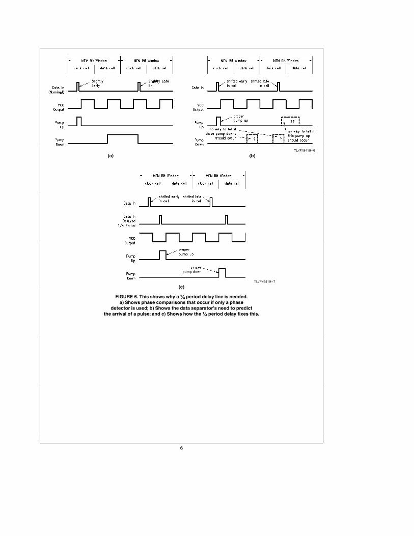
TL/F/9419–6
(a) (b)
TL/F/9419–7
(c)
FIGURE 6. This shows why a (/4 period delay line is needed.
a) Shows phase comparisons that occur if only a phase
detector is used; b) Shows the data separator’s need to predict
the arrival of a pulse; and c) Shows how the (/4 period delay fixes this.
6
2.6 Operation of an Analog Data Separator
A data separator can be described as operating in one of
three phases during each read cycle: Idle Phase, Initial
Locking Phase, and the Tracking Phase.
Initially, when the data separator is not being used to read
data from the disk, it is in the Idle Phase. While in the Idle
Phase, the PLL is both phase and frequency locked to a
reference frequency. (Frequency comparison is implement-
ed by forcing a phase comparison every VCO clock.) The
PLL must eventually lock to both clock and data pulses of
the encoded data when it is read from the disk, so the refer-
ence frequency is generally two times the data rate frequen-
cy.
When data is to be read from the disk, the PLL switches
from the reference frequency to the incoming data stream.
Because the encoded data read from the disk is not a peri-
odic signal, only phase comparisons are made. Since the
PLL was initially locked to a frequency very close to twice
the actual data rate, the time required for the PLL to lock
onto the data read from the disk is minimized.
To further minimize this locking time, the beginning of each
Address Field and Data Field starts with a preamble (or syn-
chronization field). The preamble is a series of bytes with a
zero data pattern (all clock pulses and no data pulses).
When read, the preamble will produce a periodic signal with
little bit jitter. The data separator can lock to this signal with
the least chance of an error. It would be ideal for the floppy
controller to switch the data separator from the Idle Phase
to the Initial Locking Phase at the beginning of a preamble
to enable the maximum amount of lock time.
Once the PLL is locked to the average frequency of the data
being read from the disk, it should simply track the data
frequency. This means tracking the slow data rate speed
variations caused by the drive motor, yet ignoring instanta-
neous bit jitter. This is the Tracking Phase. The data separa-
tor then allows the controller’s deserializer to start decoding
the incoming data.
2.7 Digital Data Separators
A second method of separating clock and data information
is to use a digital data separator. While the circuits for the
analog solution has evolved significantly, digital data sepa-
rators have also improved somewhat, in a (less than suc-
cessful) attempt to match the performance of the analog
approach. These circuits are described below.
First Generation Digital Data Separator (DDS)ÐThis circuit
is a very convenient all digital data separator. Its primary
advantages are simplicity, and low external parts count. This
circuit usually consists of a set of counter timing circuits and
some control logic to count times between individual pulses,
and thus determine whether a pulse is clock or data. The
SMC9216 is representative of this technology. Its major dis-
advantage is performance, and the inability to optimize the
window margin for various lock ranges. The dynamic win-
dow margin for these types of circuits is usually around 55%
with no MSV and as low as 30% with a g3% total MSV.
Second Generation DDSÐA sophisticated digital data sep-
arator can be compared functionally to an analog data sep-
arator. The ideal digital separator consists of a sampler
(phase detector), a ROM look up table, with memory (filter),
and a programmable counter (VCO). The pulse gate can be
implemented as an extension of the ROM look up table.
These circuits are typically much better than 1st generation
circuits, but still far short of the analog approach. These
circuits have dynamic window margins of 50–55% over ag6% lock range (total MSV variation).
3.0 DP8473 DATA SEPARATOR FUNCTIONAL
DESCRIPTION
The integrated floppy disk data separator from National
Semiconductor combine the performance of an analog PLL
and the ease of use of a digital data separator. It does not
require any external trimmed components, and it has a data
rate range from 125 Kbits/sec up through 1.0 Mbits/sec. It
is built using CMOS technology to achieve good linear per-
formance as well as low power operation. A block diagram
for the data separator is shown in Figure 7.
3.1 Block Diagram Description
The heart of the DP8473 data separator is the main PLL.
The main PLL consists of the VCO, programmable divider,
phase detector, and the charge pump. The entire operation
of the PLL and data separator logic is based on the Refer-
ence Clock which should be an accurate reference frequen-
cy. The Reference Clock is divided by two, then feeds the
Secondary PLL, and the divide-by-N counter. As discussed
later the Secondary PLL is used to calibrate the operation of
the quarter period delay and Primary VCO. The Reference
Clock’s Divide-By-N counter and the Programmable Divider
are both programmable counters whose divide by factor is
determined by the data rate selected. The output of the di-
vide-by-N and the Programmable divider is always twice the
data rate. The output of the divide-by-N is used as a refer-
ence frequency for the PLL to lock to when the PLL is idle.
The output of the Programmable Divider is the separated
clock that is used to strobe the incoming pulses into the
controller’s deserializer.
Note: Throughout this discussion, the Reference Clock as shown inFigure 7
is the master clock for the data separator block. This Reference Clock
also generates several other clock frequencies that are used by the
data separator sub-sections. In the following discussions the term
Reference Clock refers only to the signal in Figure 7 that feeds the
divide-by-2 and divide-by-N blocks. Also the term Divide-By-N counter
is used for the counter driven by the Reference Clock, whereas the
Programmable Divider refers to the counter driven by the VCO.
In the DP8473, the Reference Clock of Figure 7 is derived
from a prescaler circuit that is operating at 24 MHz. The
output of this prescaler circuit is 8 MHz for all data rates
except 300 Kb/s. At 300 Kb/s the equivalent prescaler out-
put is 9.6 MHz. The 24 MHz is intended to be a fixed fre-
quency, but could be scaled lower for unique applications if
desired.
Under normal operation the Secondary PLL and the Primary
VCO run at one half the Reference Clock frequency. Thus
the Primary VCO’s output is 4 MHz (except at 300 Kb/s
where the VCO output is 4.8 MHz.) Operation at different
data rates is accomplished by changing the Divide-By-N and
Programmable Divider.
The basic operation of the Phase Locked Loop is fairly stan-
dard although there are several added features in the
DP8473 PLL. The phase detector determines the phase
7
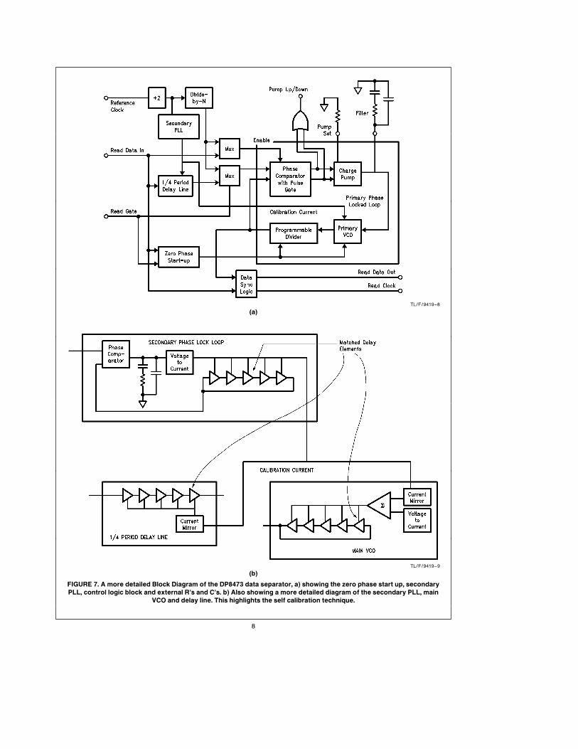
TL/F/9419–8
(a)
TL/F/9419–9
(b)
FIGURE 7. A more detailed Block Diagram of the DP8473 data separator, a) showing the zero phase start up, secondary
PLL, control logic block and external R’s and C’s. b) Also showing a more detailed diagram of the secondary PLL, main
VCO and delay line. This highlights the self calibration technique.
8
difference between two inputs. One input is always the di-
vided output of the Programmable Divider.
The other input is either a reference frequency (derived from
the Reference Clock) of twice the data rate while the data
separator is in the idle mode, or when reading the disk the
encoded data from the drive after it has passed through the
quarter-period delay line.
While in the idle mode, the phase detector determines both
phase and frequency information. This is accomplished by
forcing the pulse gate to enable all phase comparisions.
This state is set by the top two multiplexers of Figure 7which in idle mode select clocks generated by the Refer-
ence Clock to enable the pulse gate on every clock edge
(hence all clocks are compared by the phase detector). By
locking to the Reference Clock generated frequencies in
both phase and frequency, the PLL is preventing from lock-
ing back to a harmonic of this frequency.
When the data separator is told to read the incoming data
pulses, Read Gate is asserted. This changes the signals
selected by the multiplexers. The top multiplexer switches
to inputting the ‘‘raw’’ read data pulses into the pulse gate,
and the bottom multiplexer sends read data delayed by a
quarter bit period to the phase detector input. When this
switch occurs, the Zero Phase Start-Up logic synchronizes
the Programmable Divider’s output to be in phase with the
very next arriving data pulse. This causes the PLL to acquire
lock to the data quicker since it is starting with a ‘‘near zero’’
phase error between the Programmable Divider and the en-
coded data.
The quarter-period delay line consists of a series of voltage
controlled delay elements. The encoded data from the disk
drive enters the beginning of the delay line. The output is
derived from the output of one of the delay elements. The
delay element used for the output depends upon the data
rate used.
When locked to either the read data pulses or the refer-
ence, the phase detector issues either a pump up signal or
a pump down signal depending upon whether the VCO
should increase or decrease its frequency. The length of
this pump signal is proportional to the amount of phase dif-
ference between the two input signals. When locked, the
phase difference between the VCO and the delayed data
will be small. In this case the width of the pump signal could
be so small that the rise time may prevent the signal from
ever being recognized by the charge pump. To ensure that
the charge pump can recognize even the smallest pump
signal, both pump up and pump down signals are asserted
at each phase comparison and the appropriate signal is ex-
tended by an amount proportional to the phase difference
between the two input signals. The pump signals are then
subtracted from each other by the charge pump. Therefore,
the rise time of the pump up or down signals will not de-
grade the performance of the charge pump.
The charge pump simply adds or removes an amount of
charge proportional to the length of the pump signal to or
from an external filter. The voltage of the external filter de-
termines the frequency produced by the VCO.
Finally a synchronized clock and serial data signal is sent to
the controller’s deserializer by the Data Synch Logic Block.
This circuit takes the output of the Programmable Divider
and the Read Data pulses, and synchronizes these two sig-
nals, by centering the read data pulse in the appropriate
Programmable Divider’s clock cycle. This allows the control-
ler to easily deserialize and decode the data pulses proper-
ly.
An additional block not shown here, but used on the
DP8473 is the filter selection logic. This logic is used to
select different filters for different data rates. The descrip-
tion and use of this circuitry is described in section 5.3.
3.2 Self Calibration
Normally, most VCO implementations would need an exter-
nal precision capacitor (maybe trimmed) to set its center
frequency. Also, the quarter period delay line would require
an external trimming resistor to set the delay to exactly a
quarter of the data rate. The actual delay of the delay ele-
ments used in these functions would normally vary from one
part to another due to normal process variations. However,
the DP8473 has been designed to eliminate the need for
these external trims. There are actually two PLLs in the
DP8473; the Primary PLL, and a Secondary PLL. The Pri-
mary PLL is used for data separation. The Secondary PLL is
used to calibrate all of the delay elements used in the chip.
This includes the quarter-period delay line and the main
VCO.
9
The VCO of the Secondary PLL is a ring oscillator of delay
elements. The amount of delay that each inverter produces
is regulated by a control voltage which is the internally con-
nected output of the Secondary PLL. The Secondary PLL is
locked to the same frequency as the Primary VCO, half of
the reference clock frequency. The delay elements used in
the secondary VCO are identical to those used in the Pri-
mary VCO and are regulated by the same control voltage.
There are also the same number of delay elements in each.
Therefore, the center frequency of the Primary VCO is inter-
nally trimmed to exactly half of the reference frequency.
Since the delay elements in the Secondary PLL have a
known delay, any number of identical elements that are set
by the calibration voltage will have a very accurate delay.
Thus the quarter period delay line is just a chain of these
delay elements that have the desired total length.
The delay elements used in the quarter-period delay line are
also of the same type used in the secondary VCO. Because
the delay of each element is accurately set by the Second-
ary PLL, there is no need for any trimmed tuning compo-
nents for any of these circuits. Essentially, the only external
passive components required for the DP8473 are for the
filter(s) (two capacitors and a resistor per data rate), and a
resistor to set the gain of the charge pump (ie. the amount
of charge pump current).
3.3 Data Separator Read Algorithm
Since the DP8473 floppy disk controller incorporates the
analog data separator, it takes advantage of close proximity
of the controller and data separator blocks to implement a
read algorithm that is much more sophisticated than previ-
ous floppy controller integrated circuits.
Before describing the details of the algorithm, a brief discus-
sion of a disk read (or write) is necessary. When the control-
ler is issued a read (or write) command, it is asked for a
specified sector. The controller starts to look at the incom-
ing MFM information. It scans this information, trying to lo-
cate the proper address field. In order to do this, the data
separator is first told to lock to the disk data, and once
locked the controller looks at the incoming information. In
most controllers, the data separator is told to look at the
data continuously until the correct sector address is found.
This makes the data separator susceptible to being thrown
out of lock, since the controller is not ‘‘watching’’ the data
separator to see if it has maintained lock through the search
process (which it can easily lose). Once the correct address
is found the controller must then ensure that the associated
data area is read, by re-locking to the incoming signal and
then reading (or writing) the data.
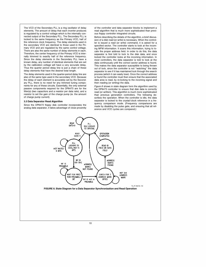
Figure 8 shows in state diagram form the algorithm used by
the DP8473 controller to ensure that disk data is correctly
read (or written). This algorithm is much more sophisticated
than previous generation controllers. The following de-
scribes the operation. When the controller is idle, the data
separator is locked to the crystal/clock reference in a fre-
quency comparison mode. (Frequency comparisons are
made by disabling the pulse gate, and ensuring that all ref-
erence and VCO cycles are compared.)
TL/F/9419–10
FIGURE 8. State Diagram for a Data Separator Synchronization and Read Operation
10
When a read command is issued to the controller the con-
troller asserts an internal Read Gate signal to the data sep-
arator. This causes the PLL to switch from locking to the
reference to locking to the data with the pulse gate enabled,
and the primary VCO/divider started in phase with the next
incoming pulse. The PLL waits 6-bit times to lock to the
data. When the seventh bit arrives the data separator as-
sumes that this bit is a preamble bit (thus an MFM clock bit).
The controller/data separator then continues looking at the
data until a non-preamble pattern is detected (ie. an MFM
data pulse). It then checks to see if it has now encountered
an address mark with the proper rule violation. If it has not,
read gate is deasserted. The data separator returns to the
idle state for 6 byte times, and then starts all over again.
If three address mark bytes are found then the data separa-
tor remains locked to the data while the controller looks to
see if it has found the right address field. If the controller
discovers that this field is not the correct address field then
it deasserts read gate for 6 bytes, and tries again.
If the correct address field is encountered, the controller de-
asserts read gate during the gap between the address and
data fields. It then re-asserts read gate, and follows the
state diagram to read the data field (ie. looking for pream-
ble, address marks etc.).
This comparison is done on a bit-by-bit basis, therefore en-
suring that the PLL never tries to lock on an unwanted field
for more than one bit time. In other words, the PLL will never
loose lock. This algorithm provides a very fast lock to the
data stream, and ensures that the data separator never falls
out of lock while reading the data. Both of these features
reduce the need to do retries of operations to ensure cor-
rect execution.
4.0 DESIGNING WITH THE DP8473
DATA SEPARATOR
The following section is a fairly in-depth description of the
design characteristics of the PLL in the DP8473 controller.
(National Semiconductor cannot be responsible for the sani-ty of any one who ventures into this section. Hence we rec-ommend using the filter values supplied in the datasheets.)
Two elements determine the overall performance of a
Phase Locked Loop: the loop gain and the loop filter design.
When using the DP8473 both of these elements are con-
trolled by the user. The amount of current in the charge
pump circuit can be set with an external resistor. This will
set the overall gain of the PLL. The filter is external to the
DP8473 and is user definable. This gives the user the possi-
bility of tailoring the data separator performance to his own
application requirements and design criteria. The following
information will present some tradeoffs that apply in choos-
ing the external components for typical applications.
4.1 Basic Phase Lock Loop Theory
This section will first start with the basic control systems
model for a second order PLL, and then apply these basic
equations to the individual blocks that compose the data
separator in the DP8473 Controller.
Initially Locked Model
In order to understand the behavior of the data separator
and to discuss the tradeoffs of the different design parame-
ters, some background in the theory of PLLs will be present-
ed.
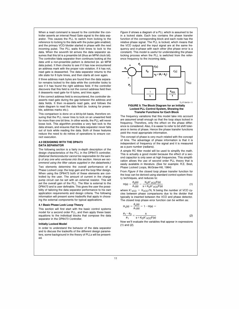
Figure 9 shows a diagram of a PLL which is assumed to be
in a locked state. Each box contains the phase transfer
function of the corresponding block and each node has the
relative phase signal. The PLL is locked, which means that
the VCO output and the input signal are at the same fre-
quency and in-phase with each other (the phase error is a
constant). This model is useful for understanding the phase
locking process when the PLL is switched from the refer-
ence frequency to the incoming data.
TL/F/9419–11
FIGURE 9. The Block Diagram for an Initially
Locked PLL Control System, Showing the
Transfer Functions for Each Block
The frequency variations that this model take into account
are assumed small enough so that the loop stays locked in
frequency. Therefore, only the effect on the phase differ-
ence is considered. Also, it is easier to refer to bit shift toler-
ance in terms of phase. Hence the phase transfer functions
yield the most appropriate information.
The concept of phase is very much related with the concept
of time. The advantage of phase information is that it is
independent of frequency of the signal and it is measured
as a pure number (radians).
A simple RC filter model will be used to simplify the math.
This is actually a good model because the effect of a sec-
ond capacitor is only seen at high frequencies. This simplifi-
cation allows the use of second order PLL theory that is
easily available in literature. (See for example: R.E. Best,
Phase Locked Loops, McGraw-Hill, 1984)
From Figure 9 the closed loop phase transfer function for
the loop can be derived using standard control system theo-
ry techniques, and reduces to:
H(s) e
i2(s)
i1(s)e
KDKÊVCOF(s)
saKDKÊVCOF(s)(1)
where KÊVCO e KVCO/N, N being the number of VCO cy-
cles between phase comparisons due to the divider that
typically is inserted between the VCO and phase detector.
The closed loop phase error function can be written as:
Hf(s) e
if(s)
i1(s)e 1bH(s) e
i1bi2
i1
e
s
saKDKÊVCOF(s)(2)
Now we’ll evaluate the variables that appear in expressions
(1) and (2).
11
The Charge Pump
In the phase detector/charge pump circuit a current is gen-
erated in the correct direction (positive or negative) every
time the edges of the VCO/divider output and the incoming
data pulses are not coincident. The current is a pulse with
amplitude equal to IPUMP and length equal to the phase
error between the two signals. The pump current is zero for
the rest of the period, so the average current is:
IZ e
IPUMPif
2 q(3)
where if is the phase error between the VCO/divider and
input pulses. The phase detector and charge pump gain is:
KD e
IZ
if
e
IPUMP
2q(4)
where IPUMP e KP c IR. IR is the current set by an external
resistor at SETCUR pin. The current at this pin is: IR e
VREF/R1, KP e 2.5, and VREF j 1.2V. Thus combining
equations:
IPUMP e
(2.5)(1.2)
R1(5)
Note that the maximum current that can flow to or from the
charge pump is 500 mA, which corresponds to a resistor
value of 3 kX. The minimum current is limited to 125 mA by
stability and leakage constraints on the internal reference
circuits. So R1 must be smaller than 12 kX. In conclusion,
the charge pump current and resistor can be set in the fol-
lowing range:
125 mA s IPUMP s 500 mA
3 kX s R1 s 12 kX
Any value in this range can be chosen, and usually the
choice is dependent on the PLL filter capacitor’s mechani-
cal size and cost. We have chosen in the datasheet a value
of 5.6 kX since it represents a good compromise of all
these considerations.
The VCO and Programmable Divider
The VCO gain is defined as the ratio between a frequency
change at the output vs. a voltage change at the input (FIL-
TER pin). This value cannot be set by the user and has
been designed to be immune to process, temperature and
voltage variation. There is a variation of less than g20%
between different parts, and the typical value of KVCO is:
KVCO e 25Mrad/sec
volt(6)
The actual value KÊVCO for expressions (1) and (2) differs by
a factor of N. N is the ratio between the frequency of the
internal VCO and the ‘‘instantaneous’’ frequency of the
data. This takes into account both the factor due to the way
the data is encoded, and the factor due to the internal pro-
grammable divider used for the data rate selection. The fol-
lowing table gives the value of N for different codes, data
rates, and data patterns. KÊVCO can be derived from these
values of N.
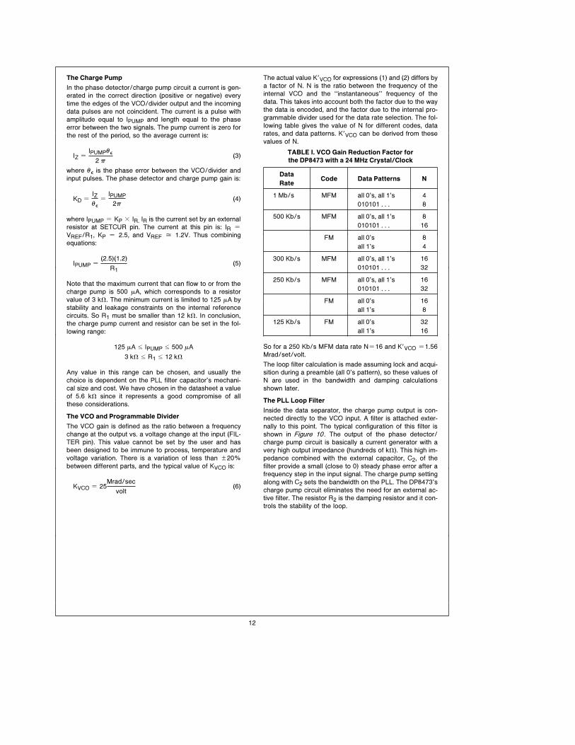
TABLE I. VCO Gain Reduction Factor for
the DP8473 with a 24 MHz Crystal/Clock
DataCode Data Patterns N
Rate
1 Mb/s MFM all 0’s, all 1’s 4
010101 . . . 8
500 Kb/s MFM all 0’s, all 1’s 8
010101 . . . 16
FM all 0’s 8
all 1’s 4
300 Kb/s MFM all 0’s, all 1’s 16
010101 . . . 32
250 Kb/s MFM all 0’s, all 1’s 16
010101 . . . 32
FM all 0’s 16
all 1’s 8
125 Kb/s FM all 0’s 32
all 1’s 16
So for a 250 Kb/s MFM data rate Ne16 and KÊVCO e1.56
Mrad/set/volt.
The loop filter calculation is made assuming lock and acqui-
sition during a preamble (all 0’s pattern), so these values of
N are used in the bandwidth and damping calculations
shown later.
The PLL Loop Filter
Inside the data separator, the charge pump output is con-
nected directly to the VCO input. A filter is attached exter-
nally to this point. The typical configuration of this filter is
shown in Figure 10. The output of the phase detector/
charge pump circuit is basically a current generator with a
very high output impedance (hundreds of kX). This high im-
pedance combined with the external capacitor, C2, of the
filter provide a small (close to 0) steady phase error after a
frequency step in the input signal. The charge pump setting
along with C2 sets the bandwidth on the PLL. The DP8473’s
charge pump circuit eliminates the need for an external ac-
tive filter. The resistor R2 is the damping resistor and it con-
trols the stability of the loop.
12
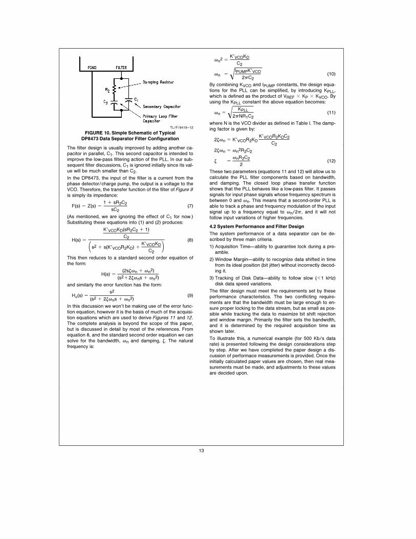
TL/F/9419–12
FIGURE 10. Simple Schematic of Typical
DP8473 Data Separator Filter Configuration
The filter design is usually improved by adding another ca-
pacitor in parallel, C1. This second capacitor is intended to
improve the low-pass filtering action of the PLL. In our sub-
sequent filter discussions, C1 is ignored initially since its val-
ue will be much smaller than C2.
In the DP8473, the input of the filter is a current from the
phase detector/charge pump, the output is a voltage to the
VCO. Therefore, the transfer function of the filter of Figure 9is simply its impedance:
F(s) e Z(s) e
1 a sR2C2
sC2(7)
(As mentioned, we are ignoring the effect of C1 for now.)
Substituting these equations into (1) and (2) produces:
H(s) e
KÊVCOKD(sR2C2 a 1)
C2#s2 a s(KÊVCOR2KD) a
KÊVCOKD
C2 J (8)
This then reduces to a standard second order equation of
the form:
H(s) e
(2sg0n a 0n2)
(s2a2g0ns a 0n2)
and similarly the error function has the form:
Hf(s) e
s2
(s2 a 2g0ns a 0n2)
(9)
In this discussion we won’t be making use of the error func-
tion equation, however it is the basis of much of the acquisi-
tion equations which are used to derive Figures 11 and 12.
The complete analysis is beyond the scope of this paper,
but is discussed in detail by most of the references. From
equation 8, and the standard second order equation we can
solve for the bandwidth, 0n and damping, g. The natural
frequency is:
0n2 e
KÊVCOKD
C2
0n e 0IPUMPKÊVCO
2qC2(10)
By combining KVCO and IPUMP constants, the design equa-
tions for the PLL can be simplified, by introducing KPLL,
which is defined as the product of VREF c KP c KVCO. By
using the KPLL constant the above equation becomes:
0n e 0 KPLL
2qNR1C2(11)
where N is the VCO divider as defined in Table I. The damp-
ing factor is given by:
2g0n e KÊVCOR2KDKÊVCOR2KDC2
C2
2g0n e 0n2R2C2
g e
0nR2C2
2(12)
These two parameters (equations 11 and 12) will allow us to
calculate the PLL filter components based on bandwidth,
and damping. The closed loop phase transfer function
shows that the PLL behaves like a low-pass filter. It passes
signals for input phase signals whose frequency spectrum is
between 0 and 0n. This means that a second-order PLL is
able to track a phase and frequency modulation of the input
signal up to a frequency equal to 0n/2q, and it will not
follow input variations of higher frequencies.
4.2 System Performance and Filter Design
The system performance of a data separator can be de-
scribed by three main criteria.
1) Acquisition TimeÐability to guarantee lock during a pre-
amble.
2) Window MarginÐability to recognize data shifted in time
from its ideal position (bit jitter) without incorrectly decod-
ing it.
3) Tracking of Disk DataÐability to follow slow (k1 kHz)
disk data speed variations.
The filter design must meet the requirements set by these
performance characteristics. The two conflicting require-
ments are that the bandwidth must be large enough to en-
sure proper locking to the data stream, but as small as pos-
sible while tracking the data to maximize bit shift rejection
and window margin. Primarily the filter sets the bandwidth,
and it is determined by the required acquisition time as
shown later.
To illustrate this, a numerical example (for 500 Kb/s data
rate) is presented following the design considerations step
by step. After we have completed the paper design a dis-
cussion of performace measurements is provided. Once the
initially calculated paper values are chosen, then real mea-
surements must be made, and adjustments to these values
are decided upon.
13
Acquisition to the Data Stream
Acquisition means to achieve phase lock and to bring the
phase error of the VCO to zero, or close to it. This includes
acquisition of phase lock to either the data input or to the
reference frequency. The lock mechanisms for these two
cases may be different.
At the moment just before Read Gate is asserted, it will be
assumed that the VCO is locked to the reference frequency.
It has been locked for a relatively long period of time, there-
fore the phase error between the VCO output and the refer-
ence frequency is nearly zero. Because the system is initial-
ly locked, the initially locked model can be used.
When Read Gate is asserted by the controller, the input to
the phase detector is switched from the reference frequen-
cy to the data stream. This is an instantaneous change of
both phase and frequency to the input of the phase detec-
tor. The loop must be designed to assure that it can achieve
both phase and frequency lock to the incoming data. Phase
and Frequency Lock implies that the steady state phase
and frequency error at the phase detector input is near zero.
The goal is to lock to the data stream within the length of
the preamble, very often half of the preamble to increase
the probability of locking successfully. In fact, during a pre-
amble the data pulses are relatively free of bit shift and the
frequency is constant. There are two basic requirements to
ensure that the data separator correctly locks to the data
stream in the required amount of time.
1. The loop bandwidth must be large enough to ensure that
phase and frequency error of the VCO goes to zero within
the required time (usually within (/2 the length of the pre-
amble). This implies that the shorter the preamble the
larger 0n.
2. The filter must also be designed to guarantee that a data
pulse will never fall out of the data window during the lock
process. The peak phase error during acquisition must be
less than (/2 of a data or clock window (i.e. or k q/2). If
the filter is incorrectlly designed and the data pulse falls
outside the window (called cycle slipping) during acquisi-
tion, the loop may never lock within the desired acquisi-
tion time and the encoded data will not be decoded cor-
rectly. This requires that to guarantee lock over a wider
variation of data rate, a larger 0n is required.
Both of these requirements can be approximately derived
from Figures 11 and 12. These curves plot relative phase
error normalized to 0n versus time in units normalized to
0n. This period of time, and the amount of phase error pres-
ent is dependent upon 0n and damping.
For the first requirement, the phase error settles close to 0
in about:
tacq e
5
0n(13)
This equation yields a minimum starting bandwidth, and is
valid for systems where the speed variation of the incoming
data is small (g1–2%).
For the second requirement, the peak phase error,
ie(PEEK), during acquisition can be determined fromFigures11 and 12. The design must ensure that the sum of this
peak phase error due to a phase step, ie(PHASE), the peak
phase error due to a frequency step, ie(FREQ), and the
phase error due to PLL noise and non-linearities, ie(PLL),
must all be less than q/2. In equation form:
ie(PEAK) e ie(FREQ) a ie(PHASE)
aie(PLL) k
q
2(14)
Thus the sum of the peak phase errors for a phase step and
a frequency step must be calculated.
TL/F/9419–13
FIGURE 11. A Plot of Normalized Phase Error of a PLL to a Phase Step Input
14
TL/F/9419–14
FIGURE 12. A Plot of Normalized Phase Error of a PLL to a Frequency Step
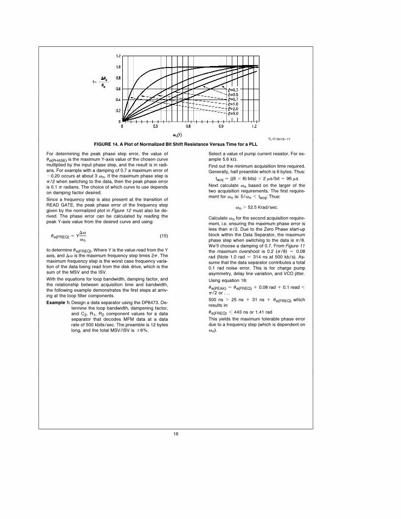
TL/F/9419–15
(a)
TL/F/9419–16
(b)
FIGURE 13. Two ‘‘Worst Case’’ Data Field Patterns for Measurement of PLL
Bit Shift Tolerance a) ‘‘11000’’ Pattern with 2/3 ms Pulse Spacing (at 500 Kb/s), and
b) A ‘‘DB6’’ (‘‘110’’) Pattern with 2/4 ms Pulse Spacing (at 500 Kb/s)
15
TL/F/9419–17
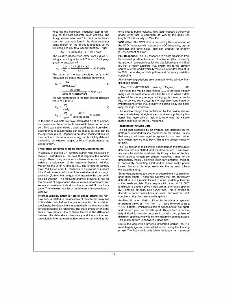
FIGURE 14. A Plot of Normalized Bit Shift Resistance Versus Time for a PLL
For determining the peak phase step error, the value of
ie(PHASE) is the maximum Y-axis value of the chosen curve
multiplied by the input phase step, and the result is in radi-
ans. For example with a damping of 0.7 a maximum error ofb0.20 occurs at about 3 0n. If the maximum phase step is
q/2 when switching to the data, then the peak phase error
is 0.1 q radians. The choice of which curve to use depends
on damping factor desired.
Since a frequency step is also present at the transition of
READ GATE, the peak phase error of the frequency step
given by the normalized plot in Figure 12 must also be de-
rived. The phase error can be calculated by reading the
peak Y-axis value from the desired curve and using:
ie(FREQ) e YD0
0n(15)
to determine ie(FREQ). Where Y is the value read from the Y
axis, and D0 is the maximum frequency step times 2q. The
maximum frequency step is the worst case frequency varia-
tion of the data being read from the disk drive, which is the
sum of the MSV and the ISV.
With the equations for loop bandwidth, damping factor, and
the relationship between acquisition time and bandwidth,
the following example demonstrates the first steps at arriv-
ing at the loop filter components.
Example 1: Design a data separator using the DP8473. De-
termine the loop bandwidth, dampening factor,
and C2, R1, R2 component values for a data
separator that decodes MFM data at a data
rate of 500 kbits/sec. The preamble is 12 bytes
long, and the total MSV/ISV is g6%.
Select a value of pump current resistor. For ex-
ample 5.6 kX.
Find out the minimum acquisition time required.
Generally, half preamble which is 6 bytes. Thus:
tacq e ((6 c 8) bits) c 2 ms/bit e 96 ms
Next calculate 0n based on the larger of the
two acquisition requirements. The first require-
ment for 0n is: 5/0n k tacq; Thus:
0n l 52.5 Krad/sec.
Calculate 0n for the second acquisition require-
ment, i.e. ensuring the maximum phase error is
less than q/2. Due to the Zero Phase start-up
block within the Data Separator, the maximum
phase step when switching to the data is q/8.
We’ll choose a damping of 0.7. From Figure 11the maximum overshoot is 0.2 (q/8) e 0.08
rad (Note 1.0 rad e 314 ns at 500 kb/s). As-
sume that the data separator contributes a total
0.1 rad noise error. This is for charge pump
asymmetry, delay line variation, and VCO jitter.
Using equation 18:
ie(PEAK) e ie(FREQ) a 0.08 rad a 0.1 read k
q/2 or . . .
500 ns l 25 ns a 31 ns a ie(FREQ) which
results in:
ie(FREQ) k 443 ns or 1.41 rad
This yields the maximum tolerable phase error
due to a frequency step (which is dependent on
0n).
16
First find the maximum frequency step in radi-
ans that the data separator must undergo. The
design requirement was 6%, but in order to ac-
count for gain variations in the data separator
some margin on top of this is required, so we
will design to 8% total speed variation. Thus:
D0 e 0.08 (500k) 2q e 251 Krad
The relative phase step error from Figure 12using a damping factor of 0.7, is Y e 0.45, plug-
ging into equation 15:
0n t
D0
ie
e
0.45 (251 Krad)
1.41e 80 Krad/s.
The larger of the two calculated 0n’s is 80
Krad/sec, so that is the chosen bandwidth.
C2 e
KPLL
2qR1N0n2
(16)
e
75 Mrad
2q(8)(5.6 kX)(80 k2)& 0.041 mF
We will round down to the next lowest standard
value of 0.039 mF.
R2 e
2g
0nC2(17)
R2 e
2g
C20n
&2(0.7)
(0.039) (80K)& 450X
In the above example we have calculated a set of compo-
nent values for the acceptable bandwidth based on acquisi-
tion. This calculation yields a good starting point from which
experimental measurements can be made, but may not be
the optimum values. Depending on other considerations we
may decide to chose a value of 0n that is slightly different
depending on window margin, or bit shift performance; as
will be shown.
Theoretical Dynamic Window Margin Determination
Previously in section 2.4 Window Margin was discussed in
terms of distortions of the data that degrade the window
margin. Here, using a model for these distortions we will
arrive at a calculation of the expected Dynamic Window
Margin for the DP8473 analog PLL. The effects of Window
error, VCO jitter, and PLL response to a previous or present
bit shift all cause a reduction of the available window margin
available. (Remember the goal is to maximize the total avail-
able bit window.) The following analysis provides a feel for
the amount of degradation due to various parameters, and
serves to provide an indicator of the expected PLL perform-
ance. The following is a list of parameters that cause loss of
window:
Internal Window Error (or static phase error): The win-
dow error is related to the accuracy of the internal delay line
in the data path before the phase detector. As explained
previously, this delay line is automatically trimmed using the
crystal frequency as reference. The static phase error is the
sum of two factors. One of these factors is the difference
between the data stream frequency and the nominal and
unavoidable internal mismatches. Another contributing fac-
tor is charge pump leakage. This factor causes a perceived
phase error that is equivalent to varying the delay line
length. This is usually l 2%–4%.
VCO Jitter: The VCO jitter is caused by the modulation of
the VCO frequency with secondary VCO frequency, crystal
oscillator and other noise. This can account for another
2–5% percent of error.
PLL Response: The PLL response to a data bit shifted from
its nominal position because of noise or jitter is directly
translated in a margin loss for the bits following any shifted
bit. For a highly accurate PLL circuit this is the primary
source of error, and it typically results in a window loss of up
to 20%, depending on data pattern and frequency variation
constraints.
All of these degradations are summed into the Window Mar-
gin specification.
iwm e ((/2 Bit Window) b ie(PLL) b ie(SWL) (18)
This yields the margin loss, where iwm is the total window
margin or the total amount of a half bit cell in which a data
pulse will be properly recognized, ie(PLL) is the error due to
PLL response, and ie(SWL) is the total error contributed by
imperfections of the PLL circuitry (including delay line accu-
racy, leakage, and noise).
The window margin loss contributed by the device accura-
cies are relatively straightforward, and are supplied by Na-
tional. The more difficult task is to determine the window
margin loss due to the PLL response.
Tracking of the Disk Data
The bit shift produced by an average disk depends on the
pattern of encoded pulses recorded on the media. Pulses
that are placed close together appear to push each other
apart when they are read back. This is the primary cause of
bit shift.
The PLL tolerance to bit shift is dependent on the amount of
data bits that are shifted, and the data pattern. It can toler-
ate more bit shift by individual bits if only a few of the bits
within a pulse stream are shifted. However, if most of the
data read by the PLL is shifted (both early and late), the loop
is constantly correcting itself and is never really phase
locked. Because it is not phase locked the maximum tolera-
ble bit shift is less.
Some data patterns are better at determining PLL perform-
ance than others. These are patterns that are particularly
difficult for a PLL remain locked to while the data pulses are
shifted early and late. For example a bit pattern of ‘‘11000’’
is difficult to decode since it has pulses alternately spaced
by 1 and 1.5 bit cells. See Figure 13a. This is difficult to
decode in some cases because under maximum bit shift
conditions all pulses are equally spaced.
Another bit pattern that is difficult to decode is a repeated
bit pattern triplet of ‘‘110’’ (or ‘‘101’’ also referred to as a
‘‘DB6’’ pattern), which has a pair of pulses one bit cell apart,
and the next pair two bit cells apart. This pattern is particu-
larly difficult to decode because it contains two pulses of
minimum spacing, followed by two maximum spaced pulses.
This pulse pattern is shown in Figure 13b.
Unlike the acquisition process described earlier, the PLL
must largely ignore individual bit shifts during the tracking
phase. The PLL should only follow the longer term average
17
data rate. The desired PLL response during the tracking
phase is somewhat different from the response required
during the acquisition phase. Instead of a high bandwidth to
decrease the lock time, a low bandwidth is preferred to pre-
vent the PLL from following individual bit shifts. When
choosing the filter bandwidth, the lowest possible value
should be used that still satisfies the acquisition time re-
quirement.
Figure 14 can be used to determine the theoretical window
margin. This curve of phase bit shift resistance plots the
amount of error introduced in the PLL’s VCO by a phase
error. The following example will show the steps involved in
calculating expected window margin, and illustrate some
concepts of tracking data.
Example 2: Determine the total dynamic window margin for
a loop with a bandwidth of 90 Krad/sec, a
damping of 0.7, and at a 500 Kb/s data rate.
The intrinsic circuit errors amount to 0.1 radi-
ans of the window. Calculate the margin for
both the 110 and 11000 pattern.
First step is to calculate the bandwidth of the
PLL while tracking these data patterns. The
bandwidth is the square root of the ratio of the
pulses per bit cell relative to preamble data,
multiplied by the bandwidth. Preamble data has
1 pulse/bit cell, and a 110 pattern has 2 pulses
per 3 bit cells, while a 1100 pattern has 4 puls-
es for every 5 cells. Thus:
0n(110) e (90 Krad/sec) c 00.66
e 72 Krad/sec
0n(11000) e (90 Krad/sec) c 00.8
e 81 Krad/sec
To analyze the problem, we need to look at
two bits. The present bit which has an early
phase step, and the next bit which has an
equal late phase step. We must determine how
large a shift in the first bit can be tolerated
such that the same amount of shift in the sec-
ond bit will still fall within the proper window. In
equation form:
ie(2) a KWMDie(1) a iPLL t iT (19)
where Die(1), the shift of the first bit, is multi-
plied by KWM, which is the affect the first bit
has on the VCO when then next bit arrives. iTis the total window available (in this case g500
ns). iPLL is the static error degradation due to
the DP847x and is 10% of 500 ns or 50 ns.
Die(2) is the maximum phase error of the sec-
ond bit. We can solve for Die(2) assuming that
Die(1) e Die(2):
Die(2) e
iT b iPLL
1a KWM (20)
The value of KWM is the value read off the y-
axis of Figure 14, at a time normalized to 0n.
This time is the time between two bits or:
For a ‘‘110’’ pattern 0n(t) e (4 ms) (72 Krad/s)e 0.29, resulting in a value from Figure 14 of
KWM e 0.37. And for a ‘‘11000’’ pattern wn(t)e (3 ms) (81 Krad/s) e 0.24, which results in
KWM e 0.28. Using 0.37, the window margin
is:
Die(2) e
500 ns b 31 ns
1.37e 342 ns
In terms of percentage this is 100*(342/500)%e 68%. Note that this is the window margin at
nominal frequency.
Open Loop Bode Plots and the Second Capacitor
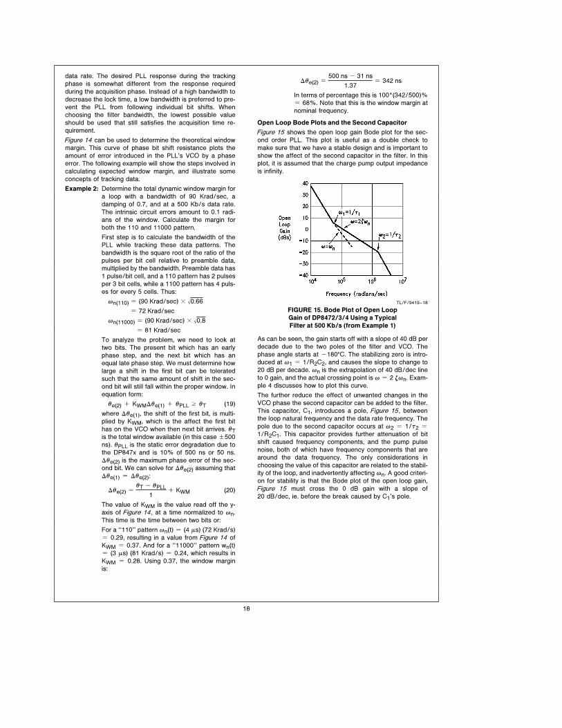
Figure 15 shows the open loop gain Bode plot for the sec-
ond order PLL. This plot is useful as a double check to
make sure that we have a stable design and is important to
show the affect of the second capacitor in the filter. In this
plot, it is assumed that the charge pump output impedance
is infinity.
TL/F/9419–18
FIGURE 15. Bode Plot of Open Loop
Gain of DP8472/3/4 Using a Typical
Filter at 500 Kb/s (from Example 1)
As can be seen, the gain starts off with a slope of 40 dB per
decade due to the two poles of the filter and VCO. The
phase angle starts at b180§C. The stabilizing zero is intro-
duced at 01 e 1/R2C2, and causes the slope to change to
20 dB per decade. 0n is the extrapolation of 40 dB/dec line
to 0 gain, and the actual crossing point is 0 e 2 g0n. Exam-
ple 4 discusses how to plot this curve.
The further reduce the effect of unwanted changes in the
VCO phase the second capacitor can be added to the filter.
This capacitor, C1, introduces a pole, Figure 15, between
the loop natural frequency and the data rate frequency. The
pole due to the second capacitor occurs at 02 e 1/u2 e
1/R2C1. This capacitor provides further attenuation of bit
shift caused frequency components, and the pump pulse
noise, both of which have frequency components that are
around the data frequency. The only considerations in
choosing the value of this capacitor are related to the stabil-
ity of the loop, and inadvertently affecting 0n. A good criteri-
on for stability is that the Bode plot of the open loop gain,
Figure 15 must cross the 0 dB gain with a slope of
20 dB/dec, ie. before the break caused by C1’s pole.
18
To determine a simple method for deriving C1, we must look
at the open loop gain of the PLL along with the transfer
function of the loop filter. The open loop gain is:
i2
i1
e
KDKÊVCO
sF(s) (21)
Where F(s) is the filters transfer function:
F(s) e Z(s) e#1asR2C2
sC1 J#sR2C1C2
(C1aC2) J (22)
Combining these two equations and manipulating we find
that the second pole occurs at:
0P e
1
R2C1(confirmingFigure 15 ) (23)
This is assuming C2 ll C1 (which we ought to assume to
maintain the validity of previous filter assumptions).
The zero introduced by C2 and R2 should be designed to be
close to the 0 dB gain crossing. Its frequency is 0z e
1/R2C2. The frequency of the pole due to R2 and C1 is
approximately 0P e 1/R2C1. This pole must not significant-
ly change the slope around the 0 dB line. If we choose C1 e
C2/20 the effect on the slope of the transfer function is less
than 1 dB/decade at the frequencies around the 0 dB gain
line crossing. Thus as a guide:
C1 s
C2
20(24)
Example 3: For example 1, determine C1.
Very simply for example 1a:
C1 s
0.039 mF
20j 2000 pF
The 1/20 factor provides the approximate value
for C1.
Example 4: Plot the Bode diagram of the open loop gain for
the DP8472 with C2 e 0.027, C1 e 1000 pF,
R1 e 5.6 kX, R2 e 545X.
There are two easy methods of doing this. One
method involves determining the open loop
gain at a low frequency, where the poles and
zeros don’t have any affect, and then using this
gain point at a start drawing the properly sloped
lines to the break point frequencies. A second
method is to calculate the 0n, and 2g0n fre-
quencies.
For the first method, first calculate the locations
of u1 and u2 in Figure 15. Thus
01 e
1
u1
e
1
R2C2
e
1
(545X)(0.027 mF)e 6.8 c 104
02 e
1
u2
e
1
R2C1
e
1
(545X)(1000 pF)e 1.8 c 106
Now pick a point that is below 01, and calculate
the open loop gain, which is:
KLOOP e 20 log Ð #KVCOKPVREF
2qR1N0 J # 1
0C2J (At 0 e 104, the KLOOP is:
KLOOP e 20 log # 12 c 106
R1C202NJ e 39 dB
Now draw a line from 0 e 104 to 01 with a
40 dB/decade slope. Then at 01 draw a line to
02 with a 20 dB/decade slope, and finally draw
a line from 02 with a 40 dB/decade slope.
To understand the affect of C1, the additional attenuation
introduced can be determined as using:
AP(w) e
1
1 a
0
0p
(25)
Using our previous example 1:
0P e
1
1000 pF 545Xe 1834 Krad, and
0 e 2q (500 kHz) e 3142 Krad/sec.
Thus
AP(w) e
1
1 a
3142
1834
e 0.37
which yields an additional 9 dB of attenuation.
Choosing Component Tolerances and Types
One of the most often asked questions is how accurate
should the filter and charge pump resistors and capacitors
be? The answer depends on how accurate a data separator
is required. For a good performance design, the following
criteria can be followed for each component:
R1: The pump set resistor’s tolerance affects the loop band-
width, 0n. The loop bandwidth directly affects window mar-
gin. Due to the square root relationship, a 5% change in this
resistor changes 0n by 2.5% which in turn affects the win-
dow margin by 1–2%. It is thus recommended that R1 be a
1% resistor. A standard carbon or metal film resistor with a
low series inductance should be chosen.
19
C2: The main filter capacitor also affects 0n in the same
way as R1 so it too should be relatively accurate. 5% is
recommended. This capacitor should be a very good quality
capacitor, with good high frequency response and low di-
electric absorption. Mica is a good choice although maybe
too expensive. Polypropalene and metal film are good as
well. Avoid Mylar or Polystyrene.
R2: This resistor has a much lower affect on window margin,
and thus standard 5% resistors can be used.
C1: The second capacitor’s accuracy in not critical 10%–
20%, but its high frequency characteristics should be quite
good, similar to a good high frequency power supply decou-
pling capacitor.
5.0 ADVANCED TOPICS
The following sections discuss several specialized areas of
evaluation and design of the PLL for the DP8473 controller.
Also a short discussion of the crystal oscillator design con-
siderations is given.
5.1 Design and Performance Testing
Testing data separators can get rather complicated. Once
the PLL circuitry, gain, bandwidth, and damping are set,
then data separator lock range testing, window margin test-
ing, and finaly bit error rate testing may be undertaken. This
testing can require some fairly sophisticated setups, and is
time consuming. To help the designer get started, a rigorous
approach to floppy disk PLL design verification is described
with reference to desired performance and available equip-
ment. If the designer is not concerned about optimum per-
formance for custom applications, then the values for the
PLL filter and pump resistor provided in the DP8473 data-
sheet should prove more than adequate.
Step 1ÐCalculating the Filter/Pump Resistor: Following
the examples above, the optimum ‘‘paper design’’ filter
components should be calculated (or use the values provid-
ed in the datasheets and tweak them).
Step 2ÐTesting Lock Range and Damping: For charac-
terization of the PLL’s acquisition, a fairly simple setup can
be used, which utilizes a pulse generator to provide a pulse
train that simulates a preamble to be input into the data
separator’s read data input. A second synchronous square-
wave that is 20–50 times the period of the data pulses is
applied to read gate. The frequency of the read data pulses
should be varied from the nominal data rate to the limits of
the desired lock range, and the lock range requirement
should be verified by monitoring the Filter pin, and the Pump
outputs. Figure 16 shows a typical setup, and some typical
waveforms on the pump and filter pins during acquisition.
Figure 16b shows a proper locking PLL which does not ex-
hibit ‘‘cycle slipping’’. Cycle slipping is denoted by the saw
tooth waveform on the filter pin, which can be seen by the
locking shown in Figure 16c.
In bothFigure 16b andc the total amplitude, DV, of the filter
pin waveform is typically less than 200 mV.
The object is to adjust the PLL bandwidth to ensure that
when locking over the desired range of data rates (for ex-
ample 500 Kb/s g6%) that no cycle slipping occurs. If slip-
ping does occur then the bandwidth should be increased.
A second piece of information that these curves provide is
verification of the damping of the PLL. As in Figure 16b the
filter pin waveform should slightly overshoot, and then (may-
be) slightly undershoot the eventual locked voltage. If there
is very little overshoot then the loop may be overdamped,
and if the filter pin voltage ‘‘rings’’ for a few cycles the loop
is probably underdamped. For example, Figure 16c not only
cycle slips, but does not overshoot, therefore the loop band-
width may be fine, and the loop is just too heavily damped.
Step 3ÐWindow Margin Evaluation: Usually to perform
this test a disk simulator should be used to simulate the
worst case drive read data conditions, and measure the er-
ror performance of the data separator. This simulator can
be used to vary the following parameters:
1. Motor Speed Variation
2. Instantaneous Speed Variation
3. Instantaneous bit shift
(to determine the window edge)
4. Data pattern.
The test setup shown in Figure 17 can accomplish some of
this testing. The disk simulator looks like a formatted disk to
the controller/data separator. To test the data separator,
software in the host computer performs a repeated series of
read operations over a period of time, while the designer
programs the disk simulator to vary the data rate from one
end of the lock range to the other. At each data rate the bit
shift is increased until the error rate increases above a mini-
mal threshold.
This testing should measure window margin over the entire
lock range, and under conditions as described in section
2.4. Typically this process is a trial-and-error process. The
bandwidth and damping can be adjusted based on the re-
sults of these tests.
20
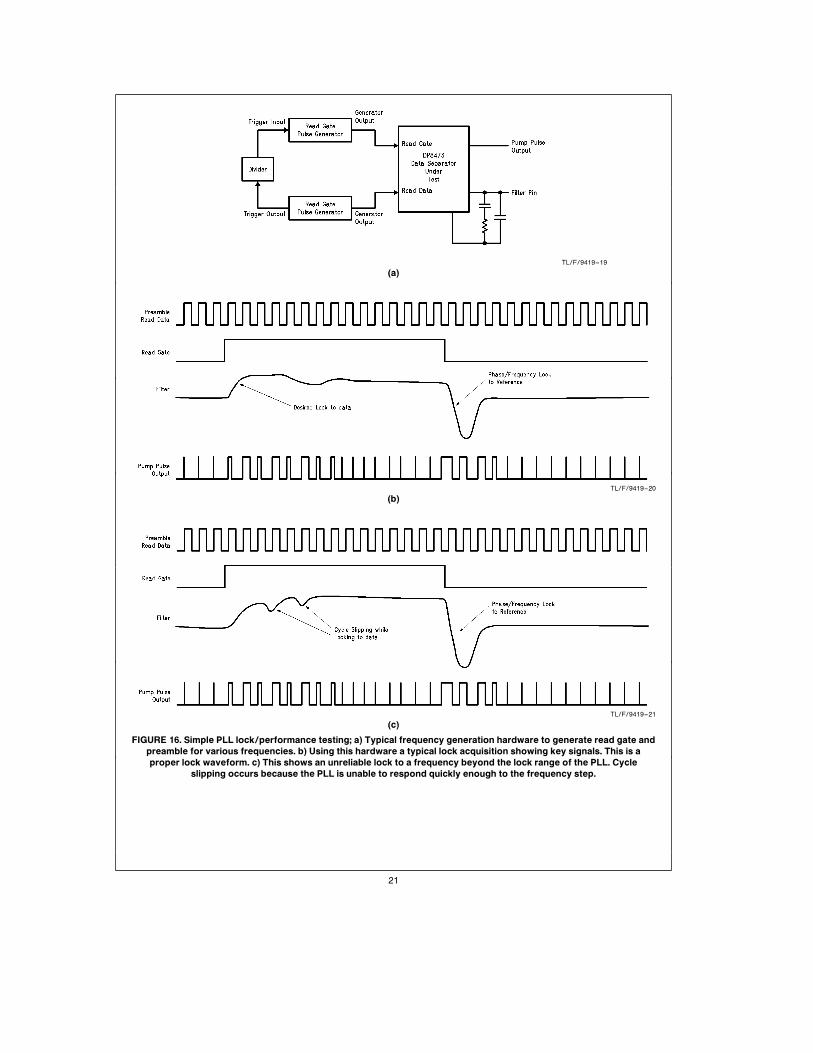
TL/F/9419–19
(a)
TL/F/9419–20
(b)
TL/F/9419–21
(c)
FIGURE 16. Simple PLL lock/performance testing; a) Typical frequency generation hardware to generate read gate and
preamble for various frequencies. b) Using this hardware a typical lock acquisition showing key signals. This is a
proper lock waveform. c) This shows an unreliable lock to a frequency beyond the lock range of the PLL. Cycle
slipping occurs because the PLL is unable to respond quickly enough to the frequency step.
21
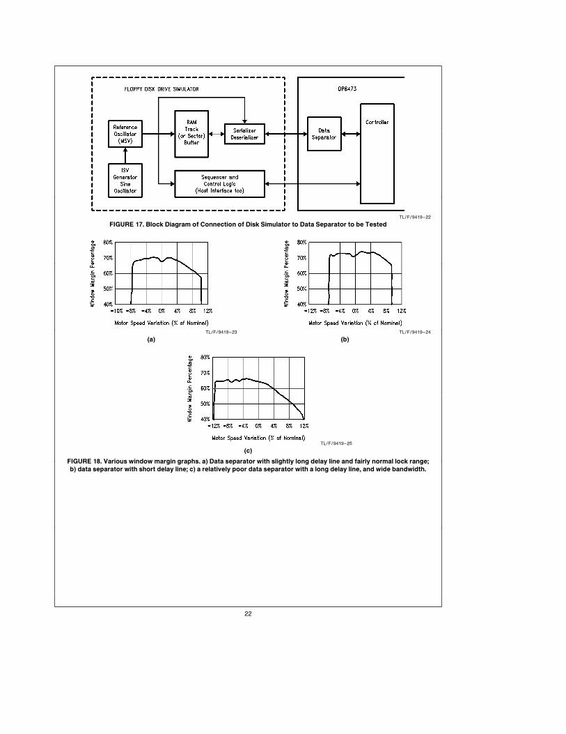
TL/F/9419–22
FIGURE 17. Block Diagram of Connection of Disk Simulator to Data Separator to be Tested
TL/F/9419–23
(a)
TL/F/9419–24
(b)
TL/F/9419–25
(c)
FIGURE 18. Various window margin graphs. a) Data separator with slightly long delay line and fairly normal lock range;
b) data separator with short delay line; c) a relatively poor data separator with a long delay line, and wide bandwidth.
22
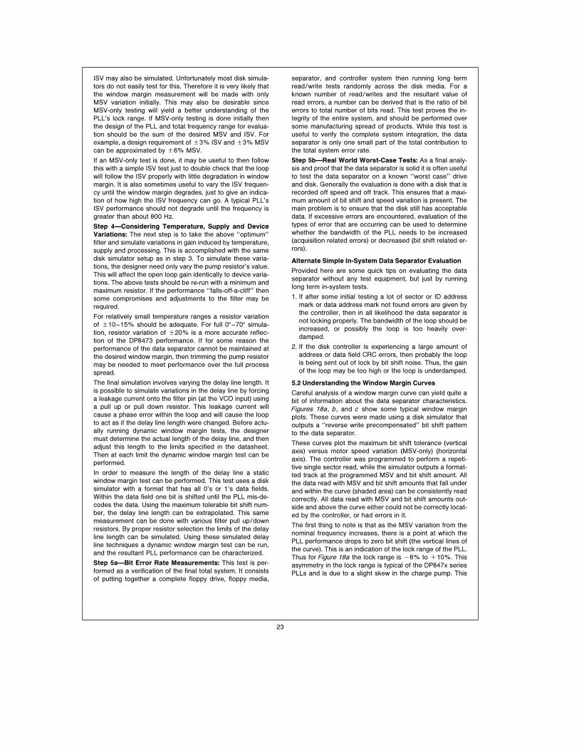
ISV may also be simulated. Unfortunately most disk simula-
tors do not easily test for this. Therefore it is very likely that
the window margin measurement will be made with only
MSV variation initially. This may also be desirable since
MSV-only testing will yield a better understanding of the
PLL’s lock range. If MSV-only testing is done initially then
the design of the PLL and total frequency range for evalua-
tion should be the sum of the desired MSV and ISV. For
example, a design requirement of g3% ISV and g3% MSV
can be approximated by g6% MSV.
If an MSV-only test is done, it may be useful to then follow
this with a simple ISV test just to double check that the loop
will follow the ISV properly with little degradation in window
margin. It is also sometimes useful to vary the ISV frequen-
cy until the window margin degrades, just to give an indica-
tion of how high the ISV frequency can go. A typical PLL’s
ISV performance should not degrade until the frequency is
greater than about 800 Hz.
Step 4ÐConsidering Temperature, Supply and Device
Variations: The next step is to take the above ‘‘optimum’’
filter and simulate variations in gain induced by temperature,
supply and processing. This is accomplished with the same
disk simulator setup as in step 3. To simulate these varia-
tions, the designer need only vary the pump resistor’s value.
This will affect the open loop gain identically to device varia-
tions. The above tests should be re-run with a minimum and
maximum resistor. If the performance ‘‘falls-off-a-cliff’’ then
some compromises and adjustments to the filter may be
required.
For relatively small temperature ranges a resistor variation
of g10–15% should be adequate. For full 0§ –70§ simula-
tion, resistor variation of g20% is a more accurate reflec-
tion of the DP8473 performance. If for some reason the
performance of the data separator cannot be maintained at
the desired window margin, then trimming the pump resistor
may be needed to meet performance over the full process
spread.
The final simulation involves varying the delay line length. It
is possible to simulate variations in the delay line by forcing
a leakage current onto the filter pin (at the VCO input) using
a pull up or pull down resistor. This leakage current will
cause a phase error within the loop and will cause the loop
to act as if the delay line length were changed. Before actu-
ally running dynamic window margin tests, the designer
must determine the actual length of the delay line, and then
adjust this length to the limits specified in the datasheet.
Then at each limit the dynamic window margin test can be
performed.
In order to measure the length of the delay line a static
window margin test can be performed. This test uses a disk
simulator with a format that has all 0’s or 1’s data fields.
Within the data field one bit is shifted until the PLL mis-de-
codes the data. Using the maximum tolerable bit shift num-
ber, the delay line length can be extrapolated. This same
measurement can be done with various filter pull up/down
resistors. By proper resistor selection the limits of the delay
line length can be simulated. Using these simulated delay
line techniques a dynamic window margin test can be run,
and the resultant PLL performance can be characterized.
Step 5aÐBit Error Rate Measurements: This test is per-
formed as a verification of the final total system. It consists
of putting together a complete floppy drive, floppy media,
separator, and controller system then running long term
read/write tests randomly across the disk media. For a
known number of read/writes and the resultant value of
read errors, a number can be derived that is the ratio of bit
errors to total number of bits read. This test proves the in-
tegrity of the entire system, and should be performed over
some manufacturing spread of products. While this test is
useful to verify the complete system integration, the data
separator is only one small part of the total contribution to
the total system error rate.
Step 5bÐReal World Worst-Case Tests: As a final analy-
sis and proof that the data separator is solid it is often useful
to test the data separator on a known ‘‘worst case’’ drive
and disk. Generally the evaluation is done with a disk that is
recorded off speed and off track. This ensures that a maxi-
mum amount of bit shift and speed variation is present. The
main problem is to ensure that the disk still has acceptable
data. If excessive errors are encountered, evaluation of the
types of error that are occurring can be used to determine
whether the bandwidth of the PLL needs to be increased
(acquisition related errors) or decreased (bit shift related er-
rors).
Alternate Simple In-System Data Separator Evaluation
Provided here are some quick tips on evaluating the data
separator without any test equipment, but just by running
long term in-system tests.
1. If after some initial testing a lot of sector or ID address
mark or data address mark not found errors are given by
the controller, then in all likelihood the data separator is
not locking properly. The bandwidth of the loop should be
increased, or possibly the loop is too heavily over-
damped.
2. If the disk controller is experiencing a large amount of
address or data field CRC errors, then probably the loop
is being sent out of lock by bit shift noise. Thus, the gain
of the loop may be too high or the loop is underdamped.
5.2 Understanding the Window Margin Curves
Careful analysis of a window margin curve can yield quite a
bit of information about the data separator characteristics.
Figures 18a, b , and c show some typical window margin
plots. These curves were made using a disk simulator that
outputs a ‘‘reverse write precompensated’’ bit shift pattern
to the data separator.
These curves plot the maximum bit shift tolerance (vertical
axis) versus motor speed variation (MSV-only) (horizontal
axis). The controller was programmed to perform a repeti-
tive single sector read, while the simulator outputs a format-
ted track at the programmed MSV and bit shift amount. All
the data read with MSV and bit shift amounts that fall under
and within the curve (shaded area) can be consistently read
correctly. All data read with MSV and bit shift amounts out-
side and above the curve either could not be correctly locat-
ed by the controller, or had errors in it.
The first thing to note is that as the MSV variation from the
nominal frequency increases, there is a point at which the
PLL performance drops to zero bit shift (the vertical lines of
the curve). This is an indication of the lock range of the PLL.
Thus for Figure 18a the lock range is b8% to a10%. This
asymmetry in the lock range is typical of the DP847x series
PLLs and is due to a slight skew in the charge pump. This
23
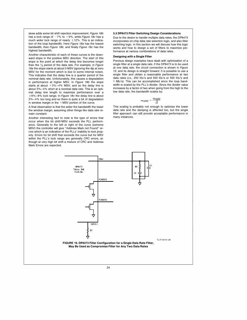
skew adds some bit shift rejection improvement. Figure 18bhas a lock range of b7% to a9%, while Figure 18c has a
much wider lock range of nearly g12%. This is an indica-
tion of the loop bandwidth. Here Figure 18a has the lowest
bandwidth, then Figure 18b, and finally Figure 18c has the
highest bandwidth.
Another characteristic of each of these curves is the down-
ward slope in the positive MSV direction. The start of this
slope is the point at which the delay line becomes longer
than the (/4 period of the data rate. For example, in Figure18a the slope starts at about 0 MSV (ignoring the dip at zero
MSV for the moment which is due to some internal noise).
This indicates that the delay line is a quarter period of the
nominal data rate. Unfortunately, this causes a degradation
in performance at higher MSV. In Figure 18b the slope
starts at about a3%–4% MSV, and so the delay line is
about 3%–4% short at a nominal data rate. This is an opti-
mal delay line length to maximize performance over ag6%–8% lock range. In Figure 18c the delay line is about
3%–4% too long and so there is quite a bit of degradation
in window margin in the aMSV portion of the curve.
A final observation is that the wider the bandwidth the lower
the window margin, assuming other things like data rate re-
main constant.
Another interesting fact to note is the type of errors that
occur when the bit shift/MSV exceeds the PLL perform-
ance. Generally to the left or right of the curve (extreme
MSV) the controller will give ‘‘Address Mark not Found’’ er-
rors which is an indication of the PLLs’ inability to lock prop-
erly. Errors for bit shift that exceeds the curve but for MSV
within the PLL’s lock range are generally CRC errors, al-
though at very high bit shift a mixture of CRC and Address
Mark Errors are expected.
5.3 DP8473 Filter Switching Design Considerations
Due to the desire to handle multiple data rates, the DP8473
incorporates on-chip data rate selection logic, and also filter
switching logic. In this section we will discuss how this logic
works and how to design a set of filters to maximize per-
formance at various combinations of data rates.
Designing with a Single Filter
Previous design examples have dealt with optimization of a
single filter at a single data rate. If the DP8473 is to be used
at one data rate, the circuit connection is shown in Figure19, and its design is straight forward. It is possible to use a
single filter and obtain a reasonable performance at two
data rates (i.e., 250 Kb/s and 500 Kb/s or 500 Kb/s and
1 Mb/s). This can be accomplished since the loop band-
width is scaled by the PLL’s divider. Since the divider value
increases by a factor of two when going from the high to the
low data rate, the bandwidth scales by:
0n250 e
0n50002This scaling is probably not enough to optimize the lower
data rate and the damping is affected too, but the single
filter approach can still provide acceptable performance in
many instances.
TL/F/9419–26
FIGURE 19. DP8473 Filter Configuration for a Single Data Rate Filter,
May Be Used as Compromise Filter for Any Two Data Rates
24
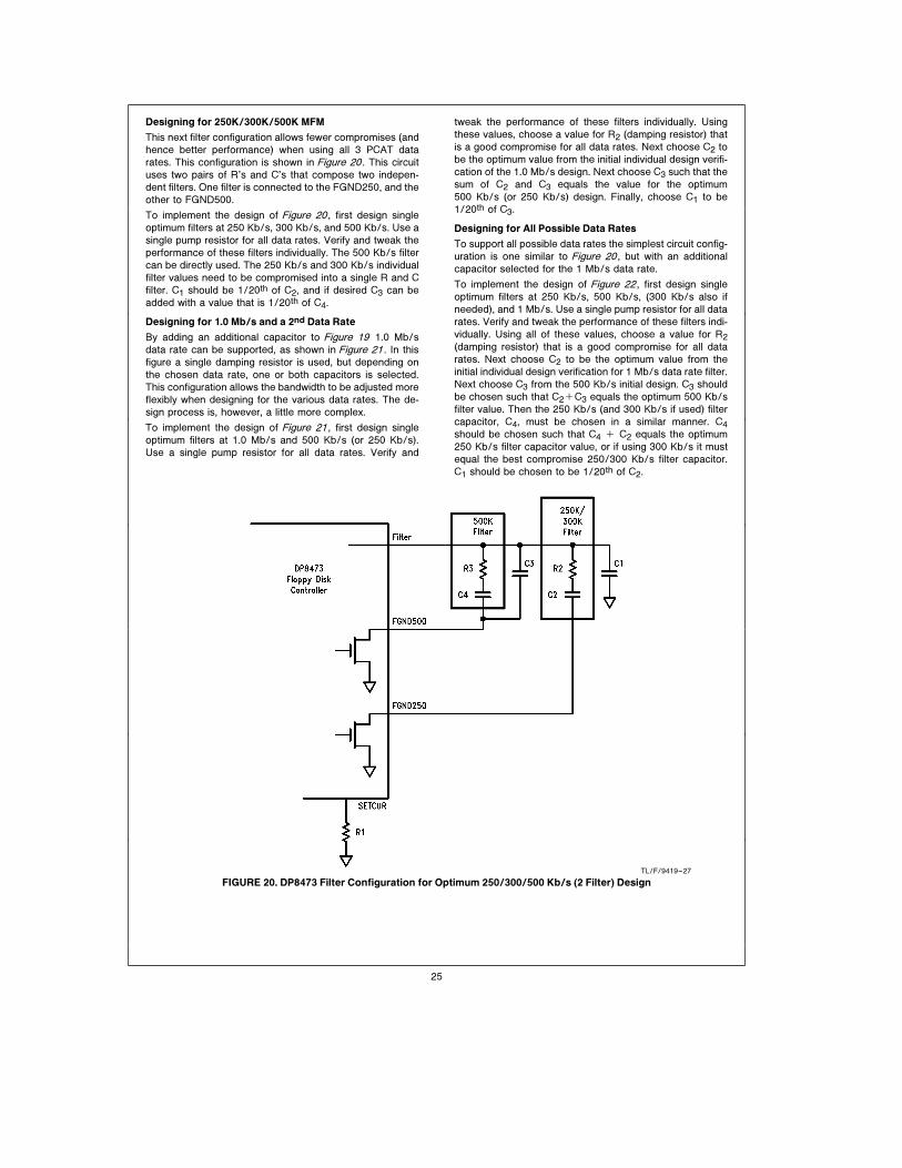
Designing for 250K/300K/500K MFM
This next filter configuration allows fewer compromises (and
hence better performance) when using all 3 PCAT data
rates. This configuration is shown in Figure 20. This circuit
uses two pairs of R’s and C’s that compose two indepen-
dent filters. One filter is connected to the FGND250, and the
other to FGND500.
To implement the design of Figure 20, first design single
optimum filters at 250 Kb/s, 300 Kb/s, and 500 Kb/s. Use a
single pump resistor for all data rates. Verify and tweak the
performance of these filters individually. The 500 Kb/s filter
can be directly used. The 250 Kb/s and 300 Kb/s individual
filter values need to be compromised into a single R and C
filter. C1 should be 1/20th of C2, and if desired C3 can be
added with a value that is 1/20th of C4.
Designing for 1.0 Mb/s and a 2nd Data Rate
By adding an additional capacitor to Figure 19 1.0 Mb/s
data rate can be supported, as shown in Figure 21. In this
figure a single damping resistor is used, but depending on
the chosen data rate, one or both capacitors is selected.
This configuration allows the bandwidth to be adjusted more
flexibly when designing for the various data rates. The de-
sign process is, however, a little more complex.
To implement the design of Figure 21, first design single
optimum filters at 1.0 Mb/s and 500 Kb/s (or 250 Kb/s).
Use a single pump resistor for all data rates. Verify and
tweak the performance of these filters individually. Using
these values, choose a value for R2 (damping resistor) that
is a good compromise for all data rates. Next choose C2 to
be the optimum value from the initial individual design verifi-
cation of the 1.0 Mb/s design. Next choose C3 such that the
sum of C2 and C3 equals the value for the optimum
500 Kb/s (or 250 Kb/s) design. Finally, choose C1 to be
1/20th of C3.
Designing for All Possible Data Rates
To support all possible data rates the simplest circuit config-
uration is one similar to Figure 20, but with an additional
capacitor selected for the 1 Mb/s data rate.
To implement the design of Figure 22, first design single
optimum filters at 250 Kb/s, 500 Kb/s, (300 Kb/s also if
needed), and 1 Mb/s. Use a single pump resistor for all data
rates. Verify and tweak the performance of these filters indi-
vidually. Using all of these values, choose a value for R2(damping resistor) that is a good compromise for all data
rates. Next choose C2 to be the optimum value from the
initial individual design verification for 1 Mb/s data rate filter.
Next choose C3 from the 500 Kb/s initial design. C3 should
be chosen such that C2aC3 equals the optimum 500 Kb/s
filter value. Then the 250 Kb/s (and 300 Kb/s if used) filter
capacitor, C4, must be chosen in a similar manner. C4should be chosen such that C4 a C2 equals the optimum
250 Kb/s filter capacitor value, or if using 300 Kb/s it must
equal the best compromise 250/300 Kb/s filter capacitor.
C1 should be chosen to be 1/20th of C2.
TL/F/9419–27
FIGURE 20. DP8473 Filter Configuration for Optimum 250/300/500 Kb/s (2 Filter) Design
25
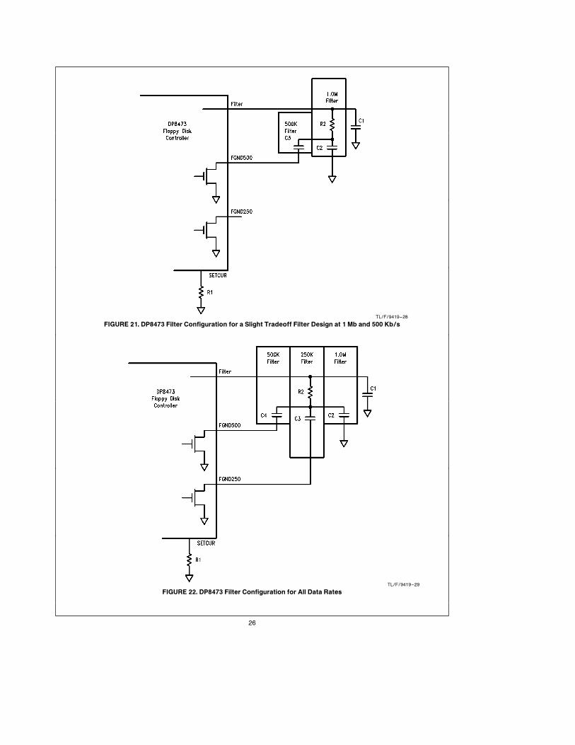
TL/F/9419–28
FIGURE 21. DP8473 Filter Configuration for a Slight Tradeoff Filter Design at 1 Mb and 500 Kb/s
TL/F/9419–29
FIGURE 22. DP8473 Filter Configuration for All Data Rates
26
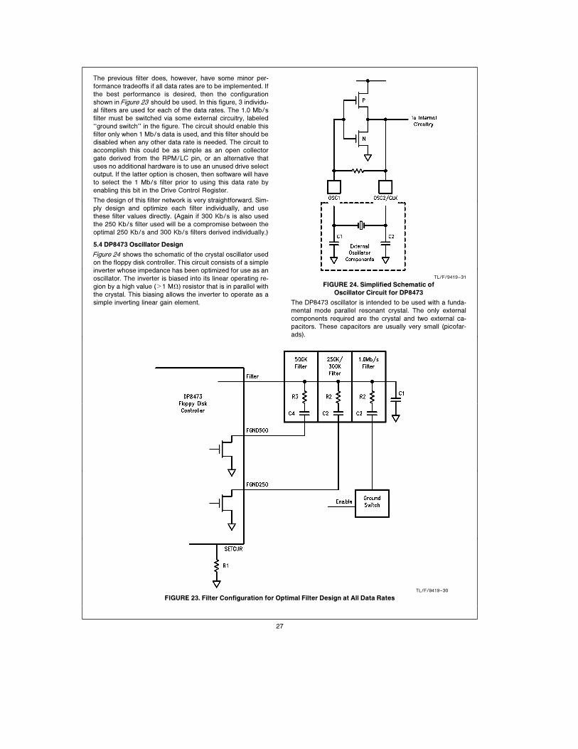
The previous filter does, however, have some minor per-
formance tradeoffs if all data rates are to be implemented. If
the best performance is desired, then the configuration
shown in Figure 23 should be used. In this figure, 3 individu-
al filters are used for each of the data rates. The 1.0 Mb/s
filter must be switched via some external circuitry, labeled
‘‘ground switch’’ in the figure. The circuit should enable this
filter only when 1 Mb/s data is used, and this filter should be
disabled when any other data rate is needed. The circuit to
accomplish this could be as simple as an open collector
gate derived from the RPM/LC pin, or an alternative that
uses no additional hardware is to use an unused drive select
output. If the latter option is chosen, then software will have
to select the 1 Mb/s filter prior to using this data rate by
enabling this bit in the Drive Control Register.
The design of this filter network is very straightforward. Sim-
ply design and optimize each filter individually, and use
these filter values directly. (Again if 300 Kb/s is also used
the 250 Kb/s filter used will be a compromise between the
optimal 250 Kb/s and 300 Kb/s filters derived individually.)
5.4 DP8473 Oscillator Design
Figure 24 shows the schematic of the crystal oscillator used
on the floppy disk controller. This circuit consists of a simple
inverter whose impedance has been optimized for use as an
oscillator. The inverter is biased into its linear operating re-
gion by a high value (l1 MX) resistor that is in parallel with
the crystal. This biasing allows the inverter to operate as a
simple inverting linear gain element.
TL/F/9419–31
FIGURE 24. Simplified Schematic of
Oscillator Circuit for DP8473
The DP8473 oscillator is intended to be used with a funda-
mental mode parallel resonant crystal. The only external
components required are the crystal and two external ca-
pacitors. These capacitors are usually very small (picofar-
ads).
TL/F/9419–30
FIGURE 23. Filter Configuration for Optimal Filter Design at All Data Rates
27
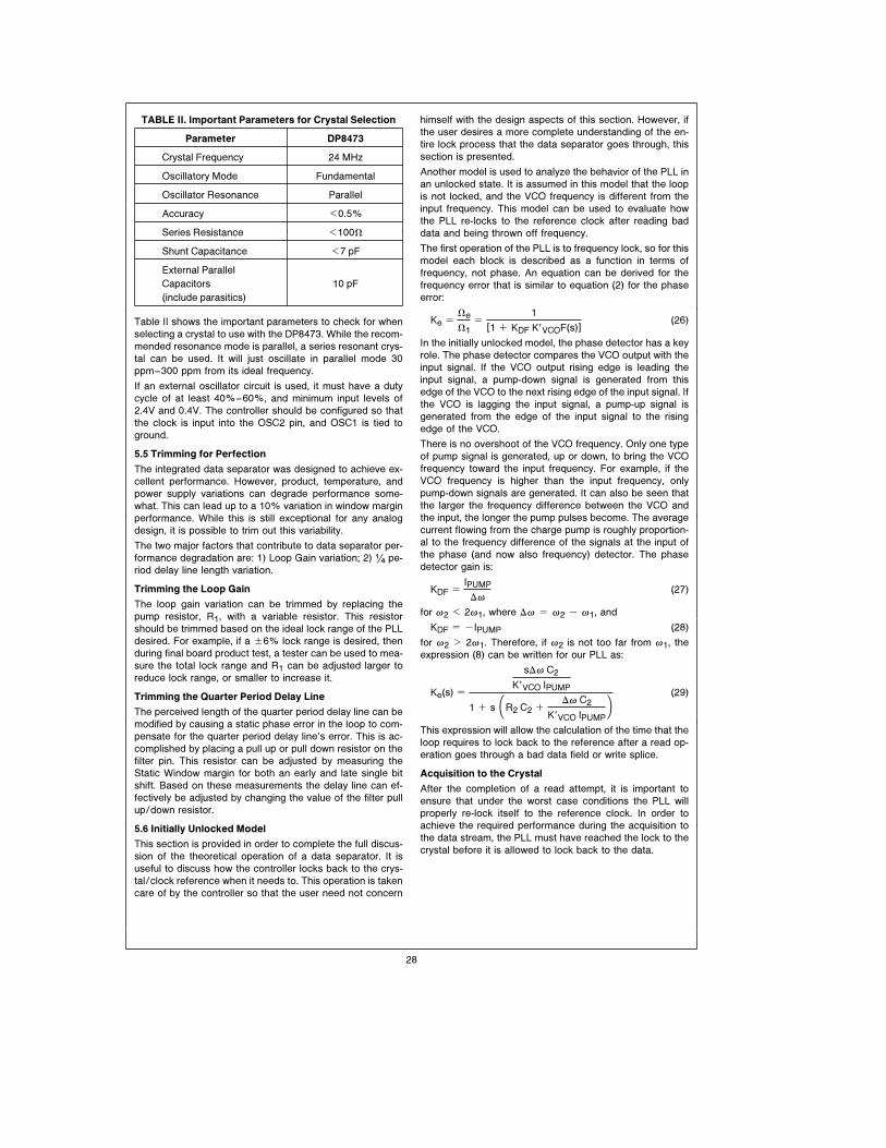
TABLE II. Important Parameters for Crystal Selection
Parameter DP8473
Crystal Frequency 24 MHz
Oscillatory Mode Fundamental
Oscillator Resonance Parallel
Accuracy k0.5%
Series Resistance k100X
Shunt Capacitance k7 pF
External Parallel
Capacitors 10 pF
(include parasitics)
Table II shows the important parameters to check for when
selecting a crystal to use with the DP8473. While the recom-
mended resonance mode is parallel, a series resonant crys-
tal can be used. It will just oscillate in parallel mode 30
ppm–300 ppm from its ideal frequency.
If an external oscillator circuit is used, it must have a duty
cycle of at least 40%–60%, and minimum input levels of
2.4V and 0.4V. The controller should be configured so that
the clock is input into the OSC2 pin, and OSC1 is tied to
ground.
5.5 Trimming for Perfection
The integrated data separator was designed to achieve ex-
cellent performance. However, product, temperature, and
power supply variations can degrade performance some-
what. This can lead up to a 10% variation in window margin
performance. While this is still exceptional for any analog
design, it is possible to trim out this variability.
The two major factors that contribute to data separator per-
formance degradation are: 1) Loop Gain variation; 2) (/4 pe-
riod delay line length variation.
Trimming the Loop Gain
The loop gain variation can be trimmed by replacing the
pump resistor, R1, with a variable resistor. This resistor
should be trimmed based on the ideal lock range of the PLL
desired. For example, if a g6% lock range is desired, then
during final board product test, a tester can be used to mea-
sure the total lock range and R1 can be adjusted larger to
reduce lock range, or smaller to increase it.
Trimming the Quarter Period Delay Line
The perceived length of the quarter period delay line can be
modified by causing a static phase error in the loop to com-
pensate for the quarter period delay line’s error. This is ac-
complished by placing a pull up or pull down resistor on the
filter pin. This resistor can be adjusted by measuring the
Static Window margin for both an early and late single bit
shift. Based on these measurements the delay line can ef-
fectively be adjusted by changing the value of the filter pull
up/down resistor.
5.6 Initially Unlocked Model
This section is provided in order to complete the full discus-
sion of the theoretical operation of a data separator. It is
useful to discuss how the controller locks back to the crys-
tal/clock reference when it needs to. This operation is taken
care of by the controller so that the user need not concern
himself with the design aspects of this section. However, if
the user desires a more complete understanding of the en-
tire lock process that the data separator goes through, this
section is presented.
Another model is used to analyze the behavior of the PLL in
an unlocked state. It is assumed in this model that the loop
is not locked, and the VCO frequency is different from the
input frequency. This model can be used to evaluate how
the PLL re-locks to the reference clock after reading bad
data and being thrown off frequency.
The first operation of the PLL is to frequency lock, so for this
model each block is described as a function in terms of
frequency, not phase. An equation can be derived for the
frequency error that is similar to equation (2) for the phase
error:
Ke e
Xe
X1
e
1
[1 a KDF KÊVCOF(s)](26)
In the initially unlocked model, the phase detector has a key
role. The phase detector compares the VCO output with the
input signal. If the VCO output rising edge is leading the
input signal, a pump-down signal is generated from this
edge of the VCO to the next rising edge of the input signal. If
the VCO is lagging the input signal, a pump-up signal is
generated from the edge of the input signal to the rising
edge of the VCO.
There is no overshoot of the VCO frequency. Only one type
of pump signal is generated, up or down, to bring the VCO
frequency toward the input frequency. For example, if the
VCO frequency is higher than the input frequency, only
pump-down signals are generated. It can also be seen that
the larger the frequency difference between the VCO and
the input, the longer the pump pulses become. The average
current flowing from the charge pump is roughly proportion-
al to the frequency difference of the signals at the input of
the phase (and now also frequency) detector. The phase
detector gain is:
KDF e
IPUMP
D0(27)
for 02 k 201, where D0 e 02 b 01, and
KDF e bIPUMP (28)
for 02 l 201. Therefore, if 02 is not too far from 01, the
expression (8) can be written for our PLL as:
Ke(s) e
sD0 C2
KÊVCO IPUMP
1 a s #R2 C2 a
D0 C2
KÊVCO IPUMPJ (29)
This expression will allow the calculation of the time that the
loop requires to lock back to the reference after a read op-
eration goes through a bad data field or write splice.
Acquisition to the Crystal
After the completion of a read attempt, it is important to
ensure that under the worst case conditions the PLL will
properly re-lock itself to the reference clock. In order to
achieve the required performance during the acquisition to
the data stream, the PLL must have reached the lock to the
crystal before it is allowed to lock back to the data.
28
If the PLL attempts to lock to a write splice the VCO may be
pulled way off frequency. To prevent this, read gate should
be deasserted as soon as a wrong or bad data field is de-
tected. This will prevent the VCO frequency from being
pulled too far away. The DP8473 read algorithm has been
optimized to prevent this.
If the PLL is locked to the data stream, when read gate is
deasserted, the lock mechanism to lock back to the refer-
ence frequency is quite similar to locking to the data. If the
frequency of the VCO has been swept way off frequency
because of a bad data field, noise, write splice, or missing
data, the unlocked PLL model must be used. Since when
locking to the crystal the phase-frequency comparison is
always enabled, the phase detector acts as a frequency
discriminator. Switching to the crystal imposes a frequency
step to the PLL. It can be demonstrated that the frequency
error generated is an exponential function of time, going to
0 with the time constant of:
TP e R2C2 a
C2D0R2N
KPLL(30)
Thus TP can be assumed to be the worst case acquisition
time to the reference clock.
Example 3: From the previous example 1, we have chosen
the values for the components of: C2 e
0.039 mF, R2 e 535X. We would like to find
the worst case time required to re-lock to the
crystal. Assume that the maximum frequency
range of the VCO is g30%.
If the VCO is pulled 30% off center, then:
D0 e 2q(500 kHz) (0.30) e 942 Krad/sec
Using equation (10) for example 1, we can ob-
tain:
TP e (0.039 mF)(545X)
a
(0.039m)(942K)(5.6KX)(8)
(75 Mrad)
TP e 41 ms
This is about 4 byte times. Thus, read gate
must be deasserted for this length of time be-
fore re-asserted to assure that the PLL has re-
locked to the reference. Most floppy control-
lers de-assert read gate much longer than this,
and the DP8473 deasserts its internal read
gate for 6 bytes.
Bibliography
Gardner, Floyd M. PhD., Phase Locked Techniques, 2nd
edition. New York: John Wiley and Sons, 1979
Best, Roland E., Phase Locked Loops, New York: McGraw-
Hill, 1984
DP8470 Phase Locked Loop Data Sheet, National Semi-
conductor Corp. 1986,7
DP8472 Floppy Disk Controller PLUS Data Sheet, National
Semiconductor Corp. 1986,7
DP8473 Floppy Disk Controller PLUS/2 Data Sheet, Nation-
al Semiconductor Corp. 1987
29
AN
-505
Flo
ppy
Dis
kD
ata
Separa
torD
esig
nG
uid
efo
rth
eD
P8473
Lit. Ý 100505
LIFE SUPPORT POLICY
NATIONAL’S PRODUCTS ARE NOT AUTHORIZED FOR USE AS CRITICAL COMPONENTS IN LIFE SUPPORT
DEVICES OR SYSTEMS WITHOUT THE EXPRESS WRITTEN APPROVAL OF THE PRESIDENT OF NATIONAL
SEMICONDUCTOR CORPORATION. As used herein:
1. Life support devices or systems are devices or 2. A critical component is any component of a life
systems which, (a) are intended for surgical implant support device or system whose failure to perform can
into the body, or (b) support or sustain life, and whose be reasonably expected to cause the failure of the life
failure to perform, when properly used in accordance support device or system, or to affect its safety or
with instructions for use provided in the labeling, can effectiveness.
be reasonably expected to result in a significant injury
to the user.
National Semiconductor National Semiconductor National Semiconductor National SemiconductorCorporation Europe Hong Kong Ltd. Japan Ltd.1111 West Bardin Road Fax: (a49) 0-180-530 85 86 13th Floor, Straight Block, Tel: 81-043-299-2309Arlington, TX 76017 Email: cnjwge@ tevm2.nsc.com Ocean Centre, 5 Canton Rd. Fax: 81-043-299-2408Tel: 1(800) 272-9959 Deutsch Tel: (a49) 0-180-530 85 85 Tsimshatsui, KowloonFax: 1(800) 737-7018 English Tel: (a49) 0-180-532 78 32 Hong Kong
Fran3ais Tel: (a49) 0-180-532 93 58 Tel: (852) 2737-1600Italiano Tel: (a49) 0-180-534 16 80 Fax: (852) 2736-9960
National does not assume any responsibility for use of any circuitry described, no circuit patent licenses are implied and National reserves the right at any time without notice to change said circuitry and specifications.