Embed Size (px)
Citation preview
8/3/2019 Floating Point Arith
http://slidepdf.com/reader/full/floating-point-arith 1/8
Quantitative Analysis of Floating Point Arithmetic on FPGA Based CustomComputing Machines
Nabeel Shirazi, A1 Walters, and Peter Athanas
Virginia Polytechnic Institute and State UniversityDepartment of Electrical Engineering
Blacksburg, Virginia 2406 1-0111
Abstract
Many algorithms rely on jloating point arithmetic
for the dynamic range of representations and require mil-
lions of calculations per second. Such computationallyintensive algorithms are candidates or acceleration using
custom computing machines (CC Ms )being tailored o r the
application. Unfortunately, jloating point operators
require excessive area (o r time} fo r conventional imple-
mentations. Instead, custom or mat s, derived fo r individ-
ual applications, are feasible on CCM s, and can be
implemented on a fraction of a single FPGA. Using
higher-level languages, like V HD L, acilitates the devel-opment of custom o perators without signifrcantly impact-
ing operator performance or area. Properties, includingarea consump tion and speed of working arithmetic opera-tor units used in real-time applications, are discussed.
1.0 Introduction
Until recently, any meaningful floating point arlth-
metic has been virtually impossible to implement on
FPGA based systems due to the limited density and speed
of older FPGAs. In addition, mapping difficulties
occurred due to the inherent complexity of floating point
arithmetic. With the introduction of high level languages
such as VHDL, rapid prototyping of floating point units
has become possible. Elaborate simulation and synthesis
tools at a higher design level aid the designer for a morecontrollable and maintainable product. Although low
level design specifications were alternately possible, the
strategy used in the work presented here was to specify
every aspect of the design in VHDL and rely on automated
synthesis to generate the FPGA mapping.
Image and digital signal processing applicationstypically require high calculation throughput [2,6]. The
arithmetic operators presented here were implemented for
real-time signal processing on the Splash-2 CCM, which
include a 2-D fast Fourier transform (FFT) and a systolic
array implementation of a FIR filter. Such signal process-
ing techniques necessitate a large dynamic range of num-
bers. The use of floating point helps to alleviate the
underflow and overflow problems often seen in fixed point
formats. An advantage of using a CC M for floating point
implementation is the ability to customize the format and
algorithm data flow to suit the application’s needs.
This paper examines the implementations of vari-
ous arithmetic operators using two floating point formats
similar to the IEEE 754 standard [5] . Eighteen and sixteenbit floating point adders/subtracters, multipliers, and
dividers have been synthesized for Xilinx 4010 FPGAs
[8]. The floating formats used are discussed in Section 2.
Sections 3, 4, and 5 present the algorithms, implementa-
tions, and optimizations used for the different operatois.
Finally a summary, in terms of size and speed, .cif thedk-
ferent floating point units is given Section6.
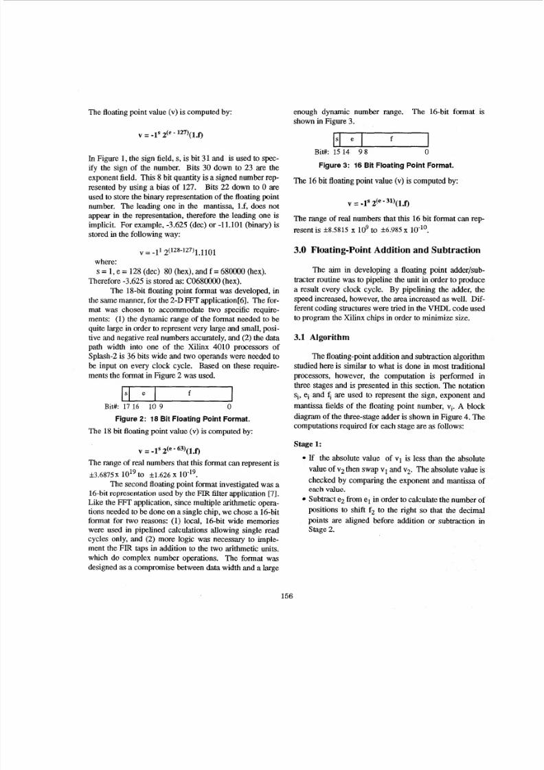
2.0 Floating Point Format R epresentation
The format which was used is similar to the BE E
754 standard used to store floating point numbers. For
comparison purposes, single precision floating point uses
the32 bit IEEE 754 format shown in Figure 1.
I s I e f IBit#: 31 30 23 22 0
Figure 1: 32 Bit Floating Point Format.
1550-8186-7086-X/9504.000 1995 EE E
8/3/2019 Floating Point Arith
http://slidepdf.com/reader/full/floating-point-arith 2/8
The floating point value (v) is computed by:
s e f
In Figure 1, the sign field,s, is bit 31 and is used to spec-
ify the sign of the number. Bits 30 down to 23 are the
exponent field. This 8 bit quantity is a signed number rep-
resented by using a bias of 127. Bits 22 down to 0 are
used to store the binary representation of the floating point
number. The leading one in the mantissa, l.f, does not
appear in the representation, therefore the leading one is
implicit. For example, -3.625 (dec) or -11.101 (binary) is
stored in the following way:
s e
= -11 2(128-127)1.1101
where:
s = 1,e = 128 (dec) 80 (hex), and f = 68oooO (hex).
Therefore -3.625 is stored as: C068oooO (hex).
The 18-bit floating point format was developed, in
the same manner, for the 2-D FFT applicationl61. The for-
mat was chosen to accommodate two specific require-
ments: (1) the dynamic range of the format needed to be
quite large in order to represent very b g e and small, posi-
tive and negative real numbers accurately, and (2) the data
path width into one of the Xilinx 4010 processors of
Splash-2 is 36 bits wide and two operands were needed to
be input on every clock cycle. Based on these require-
ments the format in Figure 2 was used.
f IBit#: 17 16 10 9 0
Figure 2: 18 Bit Floating Point Format.
The 18 bit floating point value (v) is computed by:
= -1s 2 ( e - 63) (1 .~
The range of real numbers that this formatcan epresent is
k3.6875X to k1.626 X
The second floating point format investigated was a
16-bit representation used by theFIR ilter application [7].
Like the FFT application, since multiple arithmetic opera-
tions needed to be done on a single chip, we chose a 16-bit
format for two reasons: (1) local, 16-bit wide memorieswere used in pipelined calculations allowing single read
cycles only, and (2) more logic was necessary to imple-
ment the FIR taps in addition to the two arithmetic units.
which do complex number operations. The format was
designed as a compromise between data width and a large
= -1s z(~3 1 ) ( 1 . ~
The range of real numbers that this 16 bit format can rep-
resent is k8.5815 x lo9 to zk6.985 x 10-l'.
3.0 Floating-point Addition and Subtraction
The aim in developing a floating point adder/sub-
tracter routine was to pipeline the unit in order to produce
a result every clock cycle. By pipelining the adder, the
speed increased, however, the area increased as well. Dif-
ferent coding structures were tried in the VHDL code used
to program the Xilinx chips in order to minimize size.
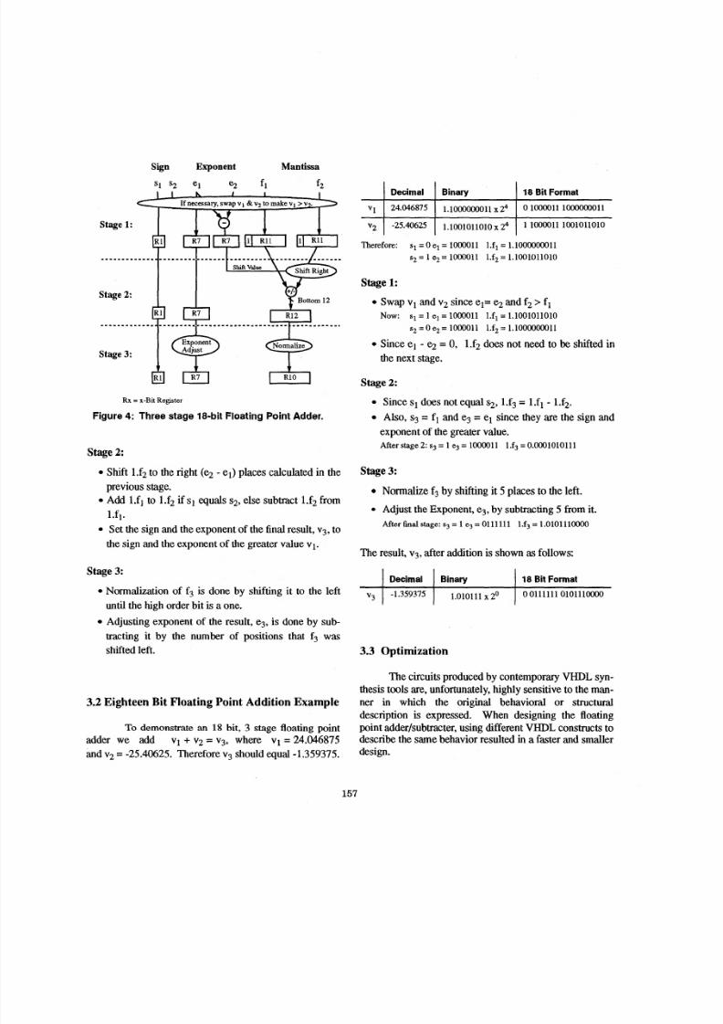
3.1 Algorithm
The floating-point addition and subtraction algorithm
studiedhere is similar to what is done in most traditional
processors, however, the computation is performed in
three stages andis
presented in this section. The notation
si, e; and fi are used to represent the sign, exponent and
mantissa fields of the floating point number, vi. A block
diagram of the three-stage adder is shown in Figure 4. The
computations required for each stage are as follows:
Stage 1:
If the absolute value of v1 is less than the absolute
value of v2 then swap v1 and v2. The absolute value is
checked by comparing the exponent and mantissa of
each value.
from el in order to calculate the number of
positions to shift f2 to the right so that the decimal
points are aligned before addition or subtraction inStage2.
Subtract
156
8/3/2019 Floating Point Arith
http://slidepdf.com/reader/full/floating-point-arith 3/8
Sign Exponent Mantissa
SI s2 el e2 f l f2
v i
Stage 3:
+
Decimal Binary 18 Bit Format
24.046875 1.100000001124 0 1000011 1000000011
Rx= x-Bit Register
Figure 4: Three stage 18-bit Floating Point Adder.
Stage 2:
Shift 1.f~o the right (% - el ) places calculated in the
Add l.fl to 1.f2 if s1 equals s2, else subtract 1.f2 from
Set the sign and the exponent of the final result, v3, to
previous stage.
1.f1.
the sign and th e exponentof the greater value vl .
Stage 3:
Normalization of f3 is done by shifting it to the left
until the high order bit is a one.
Adjusting exponent of the result, e3, is done by sub-
tracting it by the number of positions that f3 was
shifted left.
3.2 Eighteen Bit Floating Point Addition Example
To demonstrate an 18 bit, 3 stage floating point
adder we add v1 + v2=v3, where v1 =24.046875
and v2 = -25.40625. Thereforev3 should equal -1.359375.
v2 I -25.40625 I 1.1~1011010~24l~oooO11 001011010
Therefore: s1 =0 el = 1000011 l.fl = 1.1000000011
s2 = 1e2= 1000011 1.f2= 1.1001011010
Stage 1:
Swap v1 and v2 since el= e2 and f2> fl
Now: s1 = 1 el = 1000011 l.fl= 1.1001011010
s 2 = 0 e 2 = 1000011 l . f 2 = l . 1 0 0 ~ l l
Since el - = 0, 1.f~ oes not need to be shifted inthe next stage.
Stage 2:
Since s1 does not equal s2,l.f3 = l.fl - 1.f2
Also, s3 = fl and e3 = el since they are the sign and
exponent of the greater value.
After stage 2: s3 = 1 e3= 1000011 l.f3=O.OOO1010111
Stage 3:
Normalize f3 by shifting it 5 places to the left.
0 Adjust the Exponent, e3, by subtracting 5 from it.
After finalstage: s3= 1e3= 0111111 l.f3 = 1.0101110000
The result, v3, after addition is shown as follows:
I Decimal I Binary I 18 Bit Format
vg 1 -1.359375 1 1.010111~20 I 00111111010111OOOO
3.3 Optimization
The circuits produced by contempomy VHDL syn-
thesis tools are, unfortunately, highly sensitive to the man-ner in which the original behavioral or structural
description is expressed. When designing the floating
point adderhubtracter, using different VHDL constructs to
describe the same behavior resulted in a faster and smaller
design.
157
8/3/2019 Floating Point Arith
http://slidepdf.com/reader/full/floating-point-arith 4/8
The parts of the adder which caused the bottleneck
were the exponent subtracter, the mantissa adderhub-
tracter and the normalization unit. An 8-bit and a 16-bit
Xilinx hard-macro adder/subtractor[8] was used in place
of VHDL code written for the exponent and mantissa
computation. This increased the overall speed of the
design even though a smaller 12-bit adder/subtracter was
replaced with a 16-bit adder/subtracter hard macro. The
h s t cut at the normalization unit resulted in a very slow
and large design. VHDLfor loops were used for the shift
left and for the code that finds the most significant bit dur-
ing normalization. In order to decrease the size and
increase the speed of the design, the for loops were
unrolled and if statements used instead.
The first method used for shifting the mantissa of the
second operand, f2, a variable number of places was origi-
nally coded in VHDL the following way:
-- Shift f2 right ediff placese-d i ff-var : e-d iff
f2-var := f2(10 clownto 0);
for i iu 1 to 11 loop
i f (e-diff-var > zero-8) then
f2_var(9 downto 0) := fa-var(l0 downt o 1) ;
fa-var(l0) := '13';
e-cliff-var : = e-diff-var - 1;
end if;
end loop;
f2_result(lO downto 0 ) <= fa-var;
Generators
Flip Flops
(Wavailable)
The second method used if statements to check each
individual bit of the shift value and shift f2 accordingly.
6% 6% same
-- Shift f2 right ediff places
i f ((e-diff(7) = '1') or (e-diff(6) = '1') or
(e-diff(5) = '1') or (e-diff(4) = '1')) then
e-diff-var(3 downto 0) := "1111";
e-diff-var(3 downto 0 ) := e-diff(3 downto 0 ) ;
else
end i f;
-- Sequential Code for shifting f2-var
f2-var := f2(10 downto 0);
if (e-diff-var(0) = '1') then
f2_var(9 downto 0) := fZ-var(l0 down to 1) ;
fZ-var(l0) := ' 0 ' ;
end i f
if (e_diffLvar(l) '1') then
f2-var(8 downto 0) := fa-var(l0 downto 2);
f2_var(lG downt o 9) := " 0 0 " ;en d if;
if (e-cliff-var(2) = '1') then
f2_va r(6 clownto 0) : = fa-var(l0 downto 4 ) ;f2_var(lO downt o 7) := "0000";
end i f
i f (e-diff-var(3) = '1') then
fz-var(2 downto 0 ) : = fZLvar(l0 downto a ) ;f2_var(lO downto 3 ) := '00000000";
end if ;
f2_result(lO downto 0) <= fa-var;
The result of using the second method is shown in
The variable 11-bit shifter became two timesable 1.smaller and three times faster.
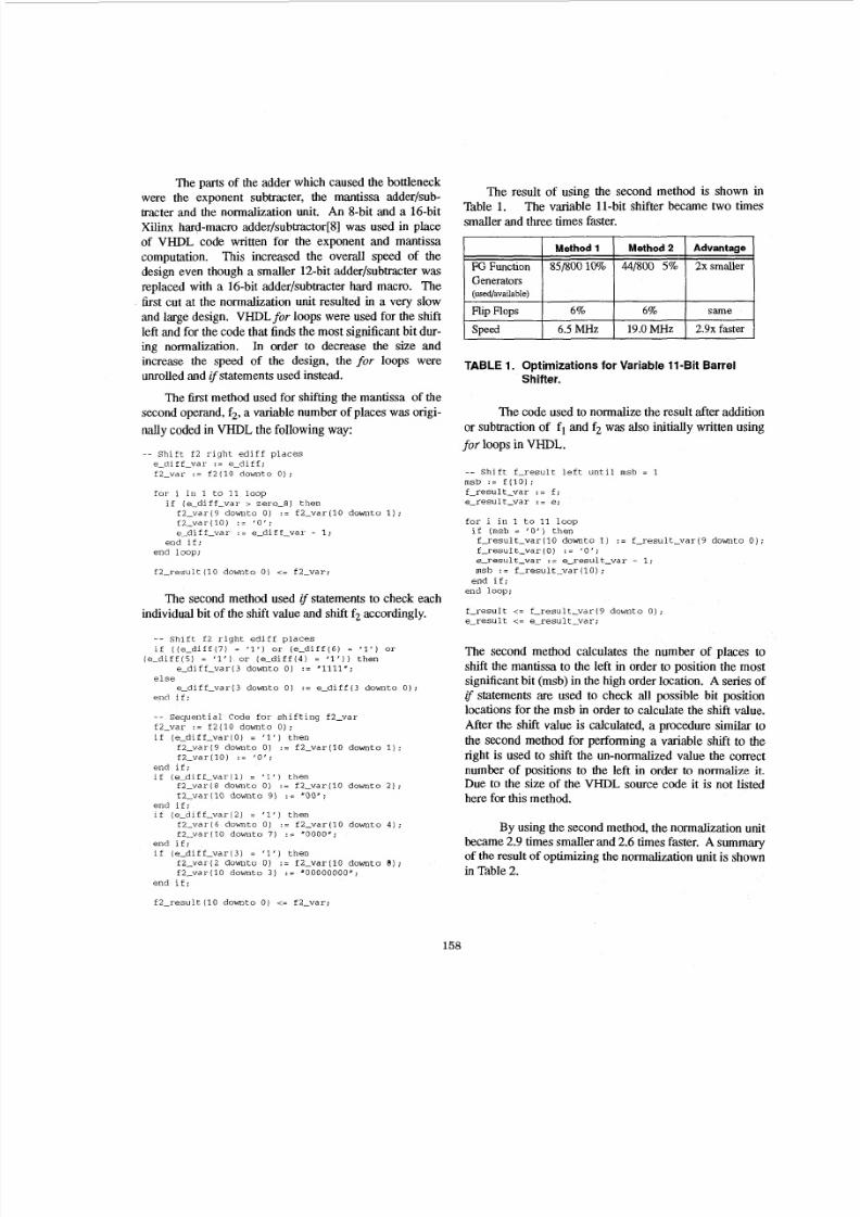
I I Method1 1 Method2 1 Advantage 1I FGFunction 85/80010% 441800 5
. . I I II speed 1 6.5 MH z 1 19.0MHz 1 2 . 9 ~aster
TABLE 1. Optimizations for Variable 11-Bit Barre lShifter.
The code used to normalize the result after additionor subtraction of fl and f2 was also initially written using
fo r loops in VHDL.
-- Shift f-result left until m s b = 1
m s b := f(10);
f-result-var := f;
e-result-var : = e ;
for i in 1 to 11 loop
if (msb = '0') then
f-result-var(l0 downto 1) := f_result_vai-(9 ownto 0);
fresult-var(0) := '0';
eresult-var := e-result-var - 1;
msb : = fLresultvar(l0);
end if;
end loop;
f-result <= f-result-var(9 downto 0)
e-result <= e-result-var;
The second method calculates the number of places to
shift the mantissa to the left in order to position the most
significant bit (msb) in the high order location. A series of
if statements are used to check all possible bit position
locations for the msb in order to calculate the shift value.
After the shift value is calculated, a procedure similar to
the second method for performing a variable shift to the
right is used to shift the un-normalized value the correct
number of positions to the left in order to normalize it.
Due to the size of the VHDL source code it is not listed
here for this method.
By using the second method, the normalization unit
became 2.9 times smaller and 2.6 times faster. A summary
of the result of optimizing the normalization unit is shown
in Table 2.
158
8/3/2019 Floating Point Arith
http://slidepdf.com/reader/full/floating-point-arith 5/8
4.1 Algorithm
FG Function 167/800 20% 58/800 7%
Generators
I I Method1 I Method2 I Advantaae I2 . 9 ~
smaller
Flip Flops
Speed
6% 6% same
5.1 MHz 13.4MHz 2 . 6 ~aster
TABLE 2. Optimizations for Normalization Unit.
The overall size and speed of the 16 and 18-bit
floating point adders are given in Section 6.
4.0 Floating Point M ultiplication
Floating point multiplication is much l i e nteger
multiplication. Because floating-point numbers are stored
in sign-magnitude form, the multiplier needs only to deal
with unsigned integer numbers and normalization. Like
the architecture of the floating point adder, the floating
point multiplier unit is a three stage pipeline that produces
a result on every clock cycle. The bottleneck of this design
was the integer multiplier. Four different methods were
used to optimize the integer multiplier in order to meet
speed and size requirements.
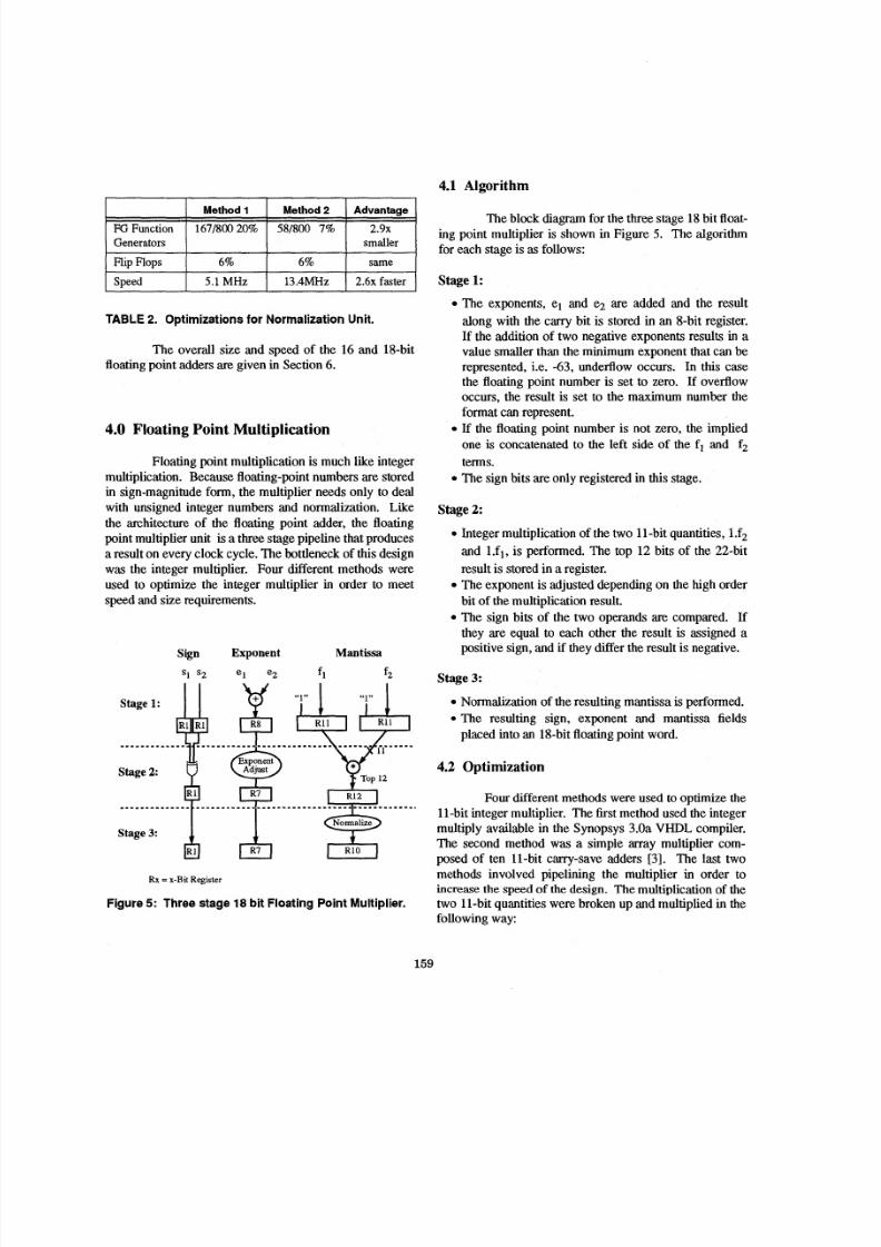
Sign Exponent Mantissa
s1 s2 el e2 f 1 f2
Rx = x-Bit Register
Figure5: Three stage 18bit Floating Point Multiplier.
The block diagram for the three stage 18 bit float-
ing point multiplier is shown in Figure 5. The algorithm
for each stage is as follows:
Stage 1:
The exponents, el and e2 are added and the result
along with the carry bit is stored in an 8-bit register.
If the addition of two negative exponents results in a
value smaller than the minimum exponent that can be
represented, i.e. -63, underflow occurs. In this case
the floating point number is set to zero. If overflow
occurs, the result is set to the maximum number the
format can represent.
If the floating point number is not zero, the implied
one is concatenated to the left side of the fl and fi
terms.
The sign bits are only registered in this stage.
Stage 2:
Integer multiplication of the two 11-bit quantities, 1.f2
and l.fl, is performed. The top 12 bits of the 22-bit
result is stored in a register.
The exponent is adjusted depending on the high order
bit of the multiplication result.
The sign bits of the two operands are compared. If
they are equal to each other the result is assigned a
positive sign, and if they differ the result is negative.
Stage 3:
Normalization of the resulting mantissa isperformed.
The resulting sign, exponent and mantissa fields
placed into an 18-bit floating point word.
4.2 Optimization
Four different methods were used to optimize the
11-bit integer multiplier. The first method used the integer
multiply available in the Synopsys 3.0a VHDL compiler.
The second method was a simple array multiplier com-
posed of ten 11-bit carry-save adders [3]. The last two
methods involved pipelining the multiplier in order to
increase the speed of h e design. The multiplication of the
two 11-bit quantities were broken up and multiplied in the
following way:
159
8/3/2019 Floating Point Arith
http://slidepdf.com/reader/full/floating-point-arith 6/8
5.1 Algorithm
Speed'
Area
Advantage
X6 X5
* Y6 Y5
X5Y5X6Y5
X5 Y 6
t X6Y6
2 2 Bit Result
4 . 9 M H z 3.7MHz 6 .2MHz 9 .4MHz
1 o 0.90 1.29 1.34
In the third method, the first stage of the multiplier was the
multiplication of the four terms X5Y5, X6Y5, X5Y6, and
X6 Y6. The second stage involved adding the results ofthe four multiplications. In method 4, two stages were
used to sum the multiplication terms.
Speed
Advantage
The results of the four methods are summarized
in Table 3. The advantage n terms of the number of times
faster and the number of times larger than Method 1 is
shown.
Generators
1o 0.75 1.24 1.92
I ~ t a a e s I 1 I 1 I 2 3 I
TABLE 3. Results from Four Methods Used toOptimize an Integer 11-Bit Multiplier.
Method 1 was used in the floating point multiplier unit
since the size of the unit wa s too large using methods 3 or
4 to allow an additional floating point unit in the same
chip. The overall size and speed of the 16 and 18-bit float-
ing point multipliers are given in Section 6, Summary and
Conclusions.
5.0 Floating Point Division
A floating-point division technique is presented
here which utilizes the pipelined multiplier discussedear-lier. Division can be done by using the reciprocal of the
divisor value so that the equation for division becomes a
multiplication of ( A x (1/B) =Q). Independent operations
on the different floatingpoint fields enable the design to be
pipelined easily.
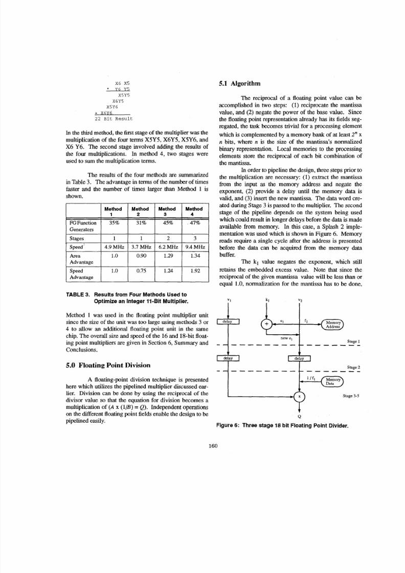
The reciprocal of a floating point value can be
accomplished in two steps: (1) reciprocate the mantissa
value, and (2) negate the power of the base value. Since
the floating point representation already has its fields seg-
regated, the task becomes trivial for a processing element
which is complemented by a memory bank of at least 2" x
n bits, where n is the size of the mantissa's normalized
binary representation. Local memories to the processing
elements store the reciprocal of each bit combination of
the mantissa.
In order to pipeline the design, three steps prior to
the multiplication are necessary: (1) extract the mantissa
from th e input as the memory address and negate the
exponent, (2) provide a delay until the memory data isvalid, and (3) insert the new mantissa. The data word cre-
ated during Stage3 is passed to the multiplier. The second
stage of the pipeline depends on the system being used
which could result in longer delays before the data is made
available from memory. In this case, a Splash 2 imple-
mentation was used which is shown in Figure 6. Memory
reads require a single cycle after th e address is presented
before the data can be acquired from the memory data
buffer.
The kl value negates the exponent, which still
retains the embedded excess value. Note that since the
reciprocal of the given mantissa value will be less than orequal 1.0, normalization for the mantissa has to be done,
+ Address
*elay r"lelay-ata
Stage 3-5YFigure 6: Three stage 18 bit Floating Point Divider.
160
8/3/2019 Floating Point Arith
http://slidepdf.com/reader/full/floating-point-arith 7/8
although a special case for 1.0 has to be made. The nor-
malization process is done automatically with k,. Once
the addition is done, the result becomes the new exponent
passed onto Stage 2. The mantissa in Stage 1 directly goes
to the memory address buffer to obtain the new mantissa,
but the old mantissa continues into Stage 2 and is replaced
in Stage 3. Stage 2 of the pipeline waits for the data to
become available from the memory. This occurs at Stage
3. The new mantissa is inserted into the final operand to
be passed to the multiplier. Although threepipeline stages
are shown here, additional stages occur due to the pipe-
lined multiplier to make a total of five stages.
FG Function
Generators
6.0 Summ ary and Conclusions
Adder/Subtracter Multiplier Divider
28% 44% 46%
The aim in designing the floating point units was topipeline each unit a sufficient number of times in order to
maximize speed and to minimize area It is important to
note that once the pipeline is full, a result is output every
clock cycle. A summary of the resulting size and speed ofthe 16 bit and 18 bit floating point units is given in Tables
4 and 5 respectively.
The Synopsys Version 3.0a VHDL compiler was
used along with the Xilinx 5.0 tools to compile the VHDL
description of the floating point arithmetic units. The Xil-
inx timing tool, xdeluy, was used to estimate the speed of
the designs.
Speed
Tested Speed
8.6 MHz 4.9 MHz 4.7MHz
10 MHz 10MHz 10MHz
I I I
Speed I 9.3MHz I 6.0MHz I 5.9MHz
FG Function
Generators
ni p Flops
Stages
TABLE 4. Summary of 16 bit Floating Point Units.
Adder/Subtracter Multiplier Divider
26 % 36% 38%
13% 13% 32%
3 3 5
To implement single precision floating point arith-
metic units on the Splash-2 architecture, the size of the
floating point arithmetic units would increase between 2
to 4 imes over the 18 bit format. A multiply unit would
requiretwo Xilinx 4010 chips and an adder/subtracter unit
I FliDFlo~s I 14% I 14% I 34% I
I Stages 1 3 1 3 1 5 1
I I I I I
TABLE 5. Summary of 18 bit Floating Point Units.
broken up into four 12-bit multipliers, allocating two per
chip[4]. We found that a 16x16 bit multiplier was the larg-
est parallel integer multiplier that could fit into a Xilinx
4010 chip. When synthesized, this multiplier used 75%of
the chip area
InputData Coefficient Data
PartialConvolution Sum
$6
Figure 7; The diagram shows a single Splash-2PE design for an FIR tap to ac complish complexmultiplication. The architecture can achiev e twofloating-point calculations per clock cyc le.
16
8/3/2019 Floating Point Arith
http://slidepdf.com/reader/full/floating-point-arith 8/8
@ Floating Point Multiply
0 Floating Point Add
0 Floating Point Subtract
- 8-Bit Delay Register
16 or 18 Bit Multiplexor
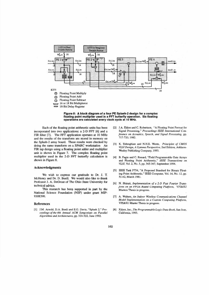
Figure 8: A block diagram of a four PE Sp~Sh-2esign for a complexfloating point multiplier used in a FFT butterfly operation. Six floatingoperations are calculated every clock cycle at 10 MHz .
Each of the floating point arithmetic units has been
incorporated into two applications: a 2-D FFT [6] and aFIR filter [7]. The FFT application operates at 10MI-Iz
and the results of the transform are stored in memory onthe Splash-2array board. These results were checked by
doing the same transform on a SPARC workstation An
FIR tap design using a floating point adder and multiplierunit is shown in Figure 7. The complex floating point
multiplier used in the 2-D FFT butterfly calculation is
shown in Figure 8.
Acknowledgments
We wish to express our gratitude to Dr. J. T,
McHenry and Dr. D. Buell. We would also like to thank
Professor J. A. DeGroat of The Ohio State University for
technicaladvice,This research has beep supported in part by the
National Science Foundation (NSF) under gmnt M I P -
9308390.
References
[I ] J.M. Arnold, D.A. Buell and E.G. Davis, “Splash 2,” Pro-ceedingsof the 4th Annual ACM Symposium on ParallelAlgorithms and Architectures,pp. 316-322, June 1992.
[2] J.A. Eldon and C. Robertson, “A Floating Point Formatfo rSignal Processing,” Proceedings IEEE International Con-ference on Acoustics, Speech, and Signal Processing, pp,717720,1982.
13) K. Eshraghian and N.H.E. Weste, Principles of CMOS
VLSIDesign,A Systems Perspective, 2nd Edition, Addison-
Wesley Publishing Company, 1993.
[4] B. Fagin and C. Renard, “Field Programmable Gate Arraysand Floating Point Arithmetic,’’ IEEE Transactions onVU], Vol. 2 , No . 3, pp. 365-367, September 1994.
[5] IEEE Task P754, “A Proposed Standard for Binary Float-ing-point Arithmetic,” IEEE Computer, Vol. 14,No. 12,pp.
51-62, March 1981.
[6] N. Shirazi, Implementation of a 2 - 0 Fast Fourier Trans-form on an FPGA Based Computing Platform, vPI&suMasters Thesis in progress.
[7] A. Walters, An Indoor Wireless Communications ChannelModel Implementation on a Custom Computing Platform,VPI&SU Master Thesis in progress.
[8] XiIinx, Inc., The Programmable Logic D ata Book, San Jose,California, 1993.
162