Embed Size (px)
Citation preview
FlexRay Communications System
Electrical Physical Layer Specification
Version 2.1 Revision B
Reg
iste
red
copy
for
cbar
baud
@cm
aiso
nneu
ve.q
c.ca
FlexRay Electrical Physical Layer Specification Disclaimer
Version 2.1 Revision B November-2006 Page 2 of 96
DISCLAIMER
This specification as released by the FlexRay Consortium is intended for the purpose of information only. The use of material contained in this specification requires membership within the FlexRay Consortium or an agreement with the FlexRay Consortium. The FlexRay Consortium will not be liable for any unauthorized use of this Specification.
Following the completion of the development of the FlexRay Communications System Specifications commercial exploitation licenses will be made available to End Users by way of an End User's License Agreement. Such licenses shall be contingent upon End Users granting reciprocal licenses to all Core Partners and non-assertions in favor of all Premium Associate Members and Associate Members.
All details and mechanisms concerning the bus guardian concept are defined in the FlexRay Bus Guardian Specifications.
The FlexRay Communications System is currently specified for a baud rate of 10 Mbit/s. It may be extended to additional baud rates.
No part of this publication may be reproduced or utilized in any form or by any means, electronic or mechanical, including photocopying and microfilm, without permission in writing from the publisher.
The word FlexRay and the FlexRay logo are registered trademarks.
Copyright © 2004-2006 FlexRay Consortium. All rights reserved.
Editor Chapters 1 - 11:
Bernd Elend, NXP Semiconductors
Editor Chapter 12:
Harald Gall, Austria Microsystems
The Core Partners of the FlexRay Consortium are BMW AG, DaimlerChrysler AG, Freescale Halbleiter Deutschland GmbH, General Motors Corporation, Philips GmbH, Robert Bosch GmbH and Volkswagen AG.
Reg
iste
red
copy
for
cbar
baud
@cm
aiso
nneu
ve.q
c.ca
FlexRay Electrical Physical Layer Specification Table of contents
Version 2.1 Revision B November-2006 Page 3 of 96
Table of contents
CHAPTER 1 INTRODUCTION ..................................................................................................................... 7
1.1 Objective............................................................................................................................................... 7
1.2 Overview............................................................................................................................................... 7
1.3 References ........................................................................................................................................... 7
1.4 Terms and definitions ........................................................................................................................... 8
1.5 List of abbreviations.............................................................................................................................. 8
1.6 Notational conventions ......................................................................................................................... 9 1.6.1 Parameter prefix conventions ......................................................................................................... 9
1.7 Important preliminary notes ................................................................................................................ 10 1.7.1 Bus speed ..................................................................................................................................... 10 1.7.2 Functional classes ........................................................................................................................ 10 1.7.3 System and conformance tests .................................................................................................... 10
1.8 Revision history .................................................................................................................................. 11 1.8.1 Changes applied to “E-PL spec v2.1 Revision A”......................................................................... 11
1.9 Open issues........................................................................................................................................ 11
CHAPTER 2 COMMUNICATION CHANNEL BASICS.............................................................................. 12
2.1 Objective............................................................................................................................................. 12
2.2 Propagation delay............................................................................................................................... 12 2.2.1 Asymmetric delay.......................................................................................................................... 13
2.3 Truncation........................................................................................................................................... 14
2.4 Symbol length change ........................................................................................................................ 15
2.5 Collisions ............................................................................................................................................ 15
2.6 EMC jitter ............................................................................................................................................ 16 2.6.1 EMC jitter on signal edges............................................................................................................ 16 2.6.2 EMC jitter on TSS-truncation ........................................................................................................ 16 2.6.3 EMC jitter on Symbol length change ............................................................................................ 16
2.7 Wake-up patterns ............................................................................................................................... 17 2.7.1 Overview ....................................................................................................................................... 17 2.7.2 Valid wake-up pattern ................................................................................................................... 17 2.7.3 Non valid wake-up patterns .......................................................................................................... 18
CHAPTER 3 PRINCIPLE OF FLEXRAY NETWORKING ......................................................................... 19
3.1 Objective............................................................................................................................................. 19
3.2 Interconnection of nodes .................................................................................................................... 19
CHAPTER 4 NETWORK COMPONENTS ................................................................................................. 21
4.1 Objective............................................................................................................................................. 21
4.2 Cables................................................................................................................................................. 21
4.3 Connectors ......................................................................................................................................... 21
Reg
iste
red
copy
for
cbar
baud
@cm
aiso
nneu
ve.q
c.ca
FlexRay Electrical Physical Layer Specification Table of contents
Version 2.1 Revision B November-2006 Page 4 of 96
4.4 Cable termination ............................................................................................................................... 22 4.4.1 Terminated cable end ................................................................................................................... 22 4.4.2 Un-terminated cable end............................................................................................................... 23
4.5 Termination concept ........................................................................................................................... 23
4.6 Common mode chokes....................................................................................................................... 24
4.7 DC bus load........................................................................................................................................ 24
CHAPTER 5 NETWORK TOPOLOGY....................................................................................................... 26
5.1 Objective............................................................................................................................................. 26
5.2 Point-to-point connection.................................................................................................................... 26
5.3 Passive star ........................................................................................................................................ 27
5.4 Linear passive bus.............................................................................................................................. 28
5.5 Active star network ............................................................................................................................. 29
5.6 Cascaded active stars ........................................................................................................................ 30
5.7 Hybrid topologies................................................................................................................................ 31
5.8 Dual channel topologies ..................................................................................................................... 31
CHAPTER 6 ELECTRICAL SIGNALING................................................................................................... 32
6.1 Objective............................................................................................................................................. 32
6.2 Overview............................................................................................................................................. 32
6.3 Bus state: Idle_LP .............................................................................................................................. 32
6.4 Bus state: Idle..................................................................................................................................... 32
6.5 Bus state: Data_1 ............................................................................................................................... 33
6.6 Bus state: Data_0 ............................................................................................................................... 33
CHAPTER 7 SIGNAL INTEGRITY............................................................................................................. 34
7.1 Objective............................................................................................................................................. 34
7.2 Definition of test planes ...................................................................................................................... 34
7.3 Eye-diagram at TP1............................................................................................................................ 35
7.4 Eye-diagram at TP4 (only valid for point-to-point connections) ......................................................... 36
CHAPTER 8 ELECTRICAL BUS DRIVER................................................................................................. 37
8.1 Overview............................................................................................................................................. 37
8.2 Operation modes ................................................................................................................................ 38 8.2.1 BD_Normal mode ......................................................................................................................... 38 8.2.2 BD_Standby mode........................................................................................................................ 38 8.2.3 BD_Sleep mode (optional)............................................................................................................ 38 8.2.4 BD_ReceiveOnly mode (optional) ................................................................................................ 38
8.3 Operation mode transitions ................................................................................................................ 39
8.4 Bus Driver – Communication Controller interface .............................................................................. 40 8.4.1 TxD/TxEN behavior in case a Bus Driver - Bus Guardian interface is implemented.................... 40 8.4.2 TxD/TxEN - behavior in case a Bus Driver - Bus Guardian interface is not implemented ........... 41 8.4.3 RxD - behavior .............................................................................................................................. 41
8.5 Bus Driver – Bus Guardian interface (optional).................................................................................. 42
Reg
iste
red
copy
for
cbar
baud
@cm
aiso
nneu
ve.q
c.ca
FlexRay Electrical Physical Layer Specification Table of contents
Version 2.1 Revision B November-2006 Page 5 of 96
8.6 Bus Driver – Host interface................................................................................................................. 43 8.6.1 Overview ....................................................................................................................................... 43 8.6.2 Hard wired signals (Option A) ....................................................................................................... 43 8.6.3 Serial Peripheral Interface (SPI) (Option B).................................................................................. 46
8.7 Bus Driver – Power supply interface .................................................................................................. 46 8.7.1 VCC supply voltage monitoring ...................................................................................................... 47 8.7.2 VBAT supply voltage monitoring ..................................................................................................... 47 8.7.3 Inhibit output (optional) ................................................................................................................. 48
8.8 Bus Driver - Level shift interface (optional) ........................................................................................ 48 8.8.1 VIO voltage monitoring................................................................................................................... 48
8.9 Bus Driver - Bus interface................................................................................................................... 49 8.9.1 Receiver characteristics................................................................................................................ 49 8.9.2 Receiver behavior ......................................................................................................................... 50 8.9.3 Receiver timing characteristics ..................................................................................................... 52 8.9.4 Receiver behavior at transition from idle to active and vice versa................................................ 54 8.9.5 Transmitter characteristics............................................................................................................ 56 8.9.6 Transmitter behavior at transition from idle to active and vice versa ........................................... 58 8.9.7 Bus Driver - bus interface behavior, when not powered............................................................... 59 8.9.8 Bus Driver - bus interface behavior under short-circuit conditions ............................................... 59
8.10 Bus Driver – Wake-up interface (optional) ....................................................................................... 60 8.10.1 Local Wake-up operating requirements...................................................................................... 60
8.11 Remote Wake-up event detector (optional)...................................................................................... 60 8.11.1 Remote Wake-up operating requirements.................................................................................. 60
8.12 Bus Driver behavior under fault conditions....................................................................................... 61 8.12.1 Environmental errors................................................................................................................... 61 8.12.2 Behavior of unconnected digital input signals ............................................................................ 62 8.12.3 Dynamic low battery voltage....................................................................................................... 63 8.12.4 Bus failure detection ................................................................................................................... 64 8.12.5 Over-temperature protection....................................................................................................... 64
8.13 Bus Driver functional classes ........................................................................................................... 65 8.13.1 Functional class “Bus Driver voltage regulator control” .............................................................. 65 8.13.2 Functional class “Bus Driver - Bus Guardian interface”.............................................................. 65 8.13.3 Functional class “Bus Driver internal voltage regulator” ............................................................. 65 8.13.4 Functional class “Bus Driver logic level adaptation” ................................................................... 65
8.14 Bus Driver signal summary............................................................................................................... 66
CHAPTER 9 ACTIVE STAR....................................................................................................................... 68
9.1 Overview............................................................................................................................................. 68
9.2 Hardware realization........................................................................................................................... 68 9.2.1 Active star - Communication Controller interface (optional) ......................................................... 69 9.2.2 Active star - Bus Guardian interface (optional) ............................................................................. 69 9.2.3 Active star - Power supply interface ............................................................................................. 69 9.2.4 Active star - Bus interface............................................................................................................. 69
9.3 Basic functionality............................................................................................................................... 69
9.4 Enhanced functionality ....................................................................................................................... 70 9.4.1 Functional class: “Active Star - Communication Controller interface” .......................................... 70 9.4.2 Functional class: “Active Star - Bus Guardian interface” .............................................................. 71 9.4.3 Functional class "Active Star - Voltage regulator control" ............................................................ 71 9.4.4 Functional class "Active Star - Internal voltage regulator"............................................................ 71
9.5 Active Star timing characteristics ....................................................................................................... 71
9.6 Active Star operation modes .............................................................................................................. 72 9.6.1 AS_Sleep ...................................................................................................................................... 72
Reg
iste
red
copy
for
cbar
baud
@cm
aiso
nneu
ve.q
c.ca
FlexRay Electrical Physical Layer Specification Table of contents
Version 2.1 Revision B November-2006 Page 6 of 96
9.6.2 AS_Normal.................................................................................................................................... 72 9.6.3 AS_Standby .................................................................................................................................. 72
9.7 Active Star operation mode transitions............................................................................................... 73 9.7.1 Active Star behavior after wake-up............................................................................................... 74
9.8 Operating states of branches ............................................................................................................. 74 9.8.1 Branch_Idle................................................................................................................................... 74 9.8.2 Branch_Active............................................................................................................................... 74 9.8.3 Branch_FailSilent.......................................................................................................................... 74
9.9 Branch operating state transitions...................................................................................................... 75
9.10 Collisions .......................................................................................................................................... 76 9.10.1 Collisions on busses ................................................................................................................... 76 9.10.2 Collision of bus activity and TxEN .............................................................................................. 76
9.11 Active Star behavior under fault conditions ...................................................................................... 78
9.12 Behavior of unconnected digital input signals .................................................................................. 79
CHAPTER 10 BUS GUARDIAN................................................................................................................. 80
CHAPTER 11 GENERAL FEATURES FOR FLEXRAY PARTS............................................................... 81
11.1 Objective........................................................................................................................................... 81
11.2 Input voltage thresholds for digital signals ....................................................................................... 81
11.3 Voltage limits for digital output signals ............................................................................................. 81
11.4 ESD protection on chip level ............................................................................................................ 82
11.5 ESD protection on ECU level ........................................................................................................... 82
11.6 Operating temperature ..................................................................................................................... 82
11.7 Serial peripheral interface (SPI) ....................................................................................................... 83 11.7.1 Behavior of unconnected digital input pins ................................................................................. 83
CHAPTER 12 SYSTEM TIMING CONSTRAINTS ..................................................................................... 84
12.1 Objective........................................................................................................................................... 84
12.2 Overview of timing parameters......................................................................................................... 84
12.3 Requirements of the decoding process according to [PS05] ........................................................... 84
12.4 FlexRay topologies ........................................................................................................................... 85 12.4.1 Signal chain ................................................................................................................................ 87 12.4.2 Example of a signal chain ........................................................................................................... 88
12.5 Description of asymmetry portions ................................................................................................... 89 12.5.1 Communication Controller .......................................................................................................... 89 12.5.2 Contribution of the Bus Driver..................................................................................................... 90 12.5.3 Interface between the Bus Driver and Communication Controller ............................................. 91 12.5.4 Passive networks ........................................................................................................................ 91 12.5.5 ECU............................................................................................................................................. 92
12.6 Requirements for Communication Controller ................................................................................... 92
12.7 Overview of the network integrity ..................................................................................................... 93
Reg
iste
red
copy
for
cbar
baud
@cm
aiso
nneu
ve.q
c.ca
FlexRay Electrical Physical Layer Specification Chapter 1: Introduction
Version 2.1 Revision B November-2006 Page 7 of 96
Chapter 1 Introduction
1.1 Objective
This specification describes the electrical physical layer for FlexRay communications systems.
1.2 Overview
The electrical physical layer for FlexRay is designed to network automotive electronic control units (ECUs). The medium that is used is dual wires. Signaling on the bus is accomplished by asserting a differential voltage between those wires. Topology variations range from linear passive busses up to active star topologies.
Furthermore the physical layer optionally incorporates a so called bus guardian as an instance, which may watch over the bus access and has the power to disable the bus access of a node module to a channel in case of mismatches in the time schedule.
This specification includes the definition of electrical characteristics of the transmission itself and also documentation of basic functionality for bus driver (BD), bus guardian (BG) and active star (AS) devices.
1.3 References
[PS05] FlexRay Communications System - Protocol Specification, v2.1 Revision A, FlexRay Consortium, December 2005
[EMC05] FlexRay Communications System - Physical Layer EMC Measurement Specification, v2.1, FlexRay Consortium, December 2005
[EPLAN06] FlexRay Communications System - Electrical Physical Layer Application Notes, v2.1 Revision B, FlexRay Consortium, November 2006
Reg
iste
red
copy
for
cbar
baud
@cm
aiso
nneu
ve.q
c.ca
FlexRay Electrical Physical Layer Specification Chapter 1: Introduction
Version 2.1 Revision B November-2006 Page 8 of 96
1.4 Terms and definitions
FlexRay specific terms and definitions are listed in [PS05].
1.5 List of abbreviations
AS: active star
BD: bus driver
BG: bus guardian
BSS: byte start sequence
CC: communication controller
ECU: electronic control unit
SPI: serial peripheral interface
TSS: transmission start sequence
uVBAT: means a voltage applied at the VBAT pin relative to ground of the semiconductor device
uVECU: means a voltage applied at the battery connector of an ECU relative to ground
X: don’t care
x: placeholder for a figure [2, 3, 4, …]
Reg
iste
red
copy
for
cbar
baud
@cm
aiso
nneu
ve.q
c.ca
FlexRay Electrical Physical Layer Specification Chapter 1: Introduction
Version 2.1 Revision B November-2006 Page 9 of 96
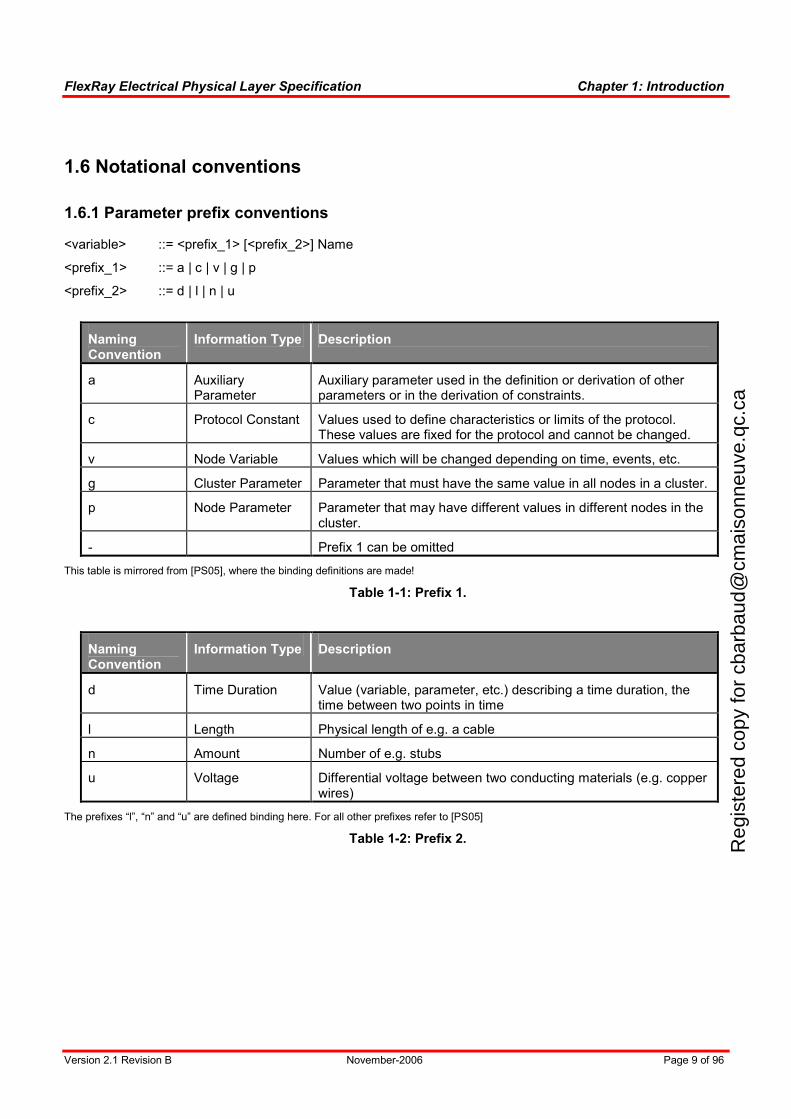
1.6 Notational conventions
1.6.1 Parameter prefix conventions
<variable> ::= <prefix_1> [<prefix_2>] Name
<prefix_1> ::= a | c | v | g | p
<prefix_2> ::= d | l | n | u
Naming Convention
Information Type Description
a Auxiliary Parameter
Auxiliary parameter used in the definition or derivation of other parameters or in the derivation of constraints.
c Protocol Constant Values used to define characteristics or limits of the protocol. These values are fixed for the protocol and cannot be changed.
v Node Variable Values which will be changed depending on time, events, etc.
g Cluster Parameter Parameter that must have the same value in all nodes in a cluster.
p Node Parameter Parameter that may have different values in different nodes in the cluster.
- Prefix 1 can be omitted
This table is mirrored from [PS05], where the binding definitions are made!
Table 1-1: Prefix 1.
Naming Convention
Information Type Description
d Time Duration Value (variable, parameter, etc.) describing a time duration, the time between two points in time
l Length Physical length of e.g. a cable
n Amount Number of e.g. stubs
u Voltage Differential voltage between two conducting materials (e.g. copper wires)
The prefixes “l”, “n” and “u” are defined binding here. For all other prefixes refer to [PS05]
Table 1-2: Prefix 2.
Reg
iste
red
copy
for
cbar
baud
@cm
aiso
nneu
ve.q
c.ca
FlexRay Electrical Physical Layer Specification Chapter 1: Introduction
Version 2.1 Revision B November-2006 Page 10 of 96
1.7 Important preliminary notes
1.7.1 Bus speed
The FlexRay communication system currently specifies for a data rate of 10MBit/s only.
Thus the nominal time of one bit (gdBit) is 100ns.
1.7.2 Functional classes
In chapters 8, 9 and 10, the physical layer devices BD, AS and the electrical interfaces of the BG are specified. This specification comprises the minimum functional features in order to ensure interoperability of FlexRay devices and compliance to constraints given by the FlexRay protocol. In addition to this, some ‘functional classes’ are introduced. Each functional class combines a set of specified options, which have to coexist when implemented. These functional classes may be implemented in order to enhance the set of functional features of FlexRay physical layer devices and make them more valuable for building automotive ECUs.
1.7.3 System and conformance tests
Tests for system behavior and FlexRay conformance are currently under development. Some basic information and prerequisites can be found in this specification. Potentially, this kind of content is to be moved when appropriate test specification documents are available.
Reg
iste
red
copy
for
cbar
baud
@cm
aiso
nneu
ve.q
c.ca
FlexRay Electrical Physical Layer Specification Chapter 1: Introduction
Version 2.1 Revision B November-2006 Page 11 of 96
1.8 Revision history
1.8.1 Changes applied to “E-PL spec v2.1 Revision A”
- Changes as listed in “Errata Sheet to E-PL v2.1 Rev. A”
- Complete reworked chapter 12
1.9 Open issues
- Chapter 10 to be updated – according to most recent BG concepts
Reg
iste
red
copy
for
cbar
baud
@cm
aiso
nneu
ve.q
c.ca
FlexRay Electrical Physical Layer Specification Chapter 2: Communication Channel basics
Version 2.1 Revision B November-2006 Page 12 of 96
Chapter 2 Communication Channel Basics
2.1 Objective
The electrical physical layer provides among other things an implementation of a FlexRay communication channel. In this section an abstract definition of the physical properties of this communication channel is given.
Any physical layer that behaves according to these basics provides a valid FlexRay communication channel.
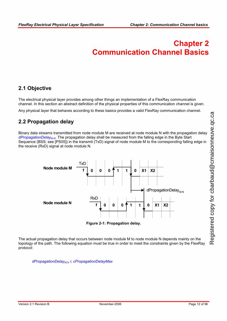
2.2 Propagation delay
Binary data streams transmitted from node module M are received at node module N with the propagation delay dPropagationDelayM,N. The propagation delay shall be measured from the falling edge in the Byte Start Sequence (BSS; see [PS05]) in the transmit (TxD) signal of node module M to the corresponding falling edge in the receive (RxD) signal at node module N.
1 0 X1 X2
TxD
RxD
0 00
1 0 X100 X2
dPropagationDelayM,N
Node module M
Node module N0
1
1
1
1
Figure 2-1: Propagation delay.
The actual propagation delay that occurs between node module M to node module N depends mainly on the topology of the path. The following equation must be true in order to meet the constraints given by the FlexRay protocol:
dPropagationDelayM,N ≤ cPropagationDelayMax
Reg
iste
red
copy
for
cbar
baud
@cm
aiso
nneu
ve.q
c.ca
FlexRay Electrical Physical Layer Specification Chapter 2: Communication Channel basics
Version 2.1 Revision B November-2006 Page 13 of 96
In [PS05] the parameter cPropagationDelayMax is limited to 2500ns. Consequently it is:
Name Description Min Max Unit
dPropagationDelayM,N Propagation delay from node module M to node module N
2500 ns
Table 2-1: Propagation delay.
See also section “Application hint: Propagation delay” in [EPLAN06].
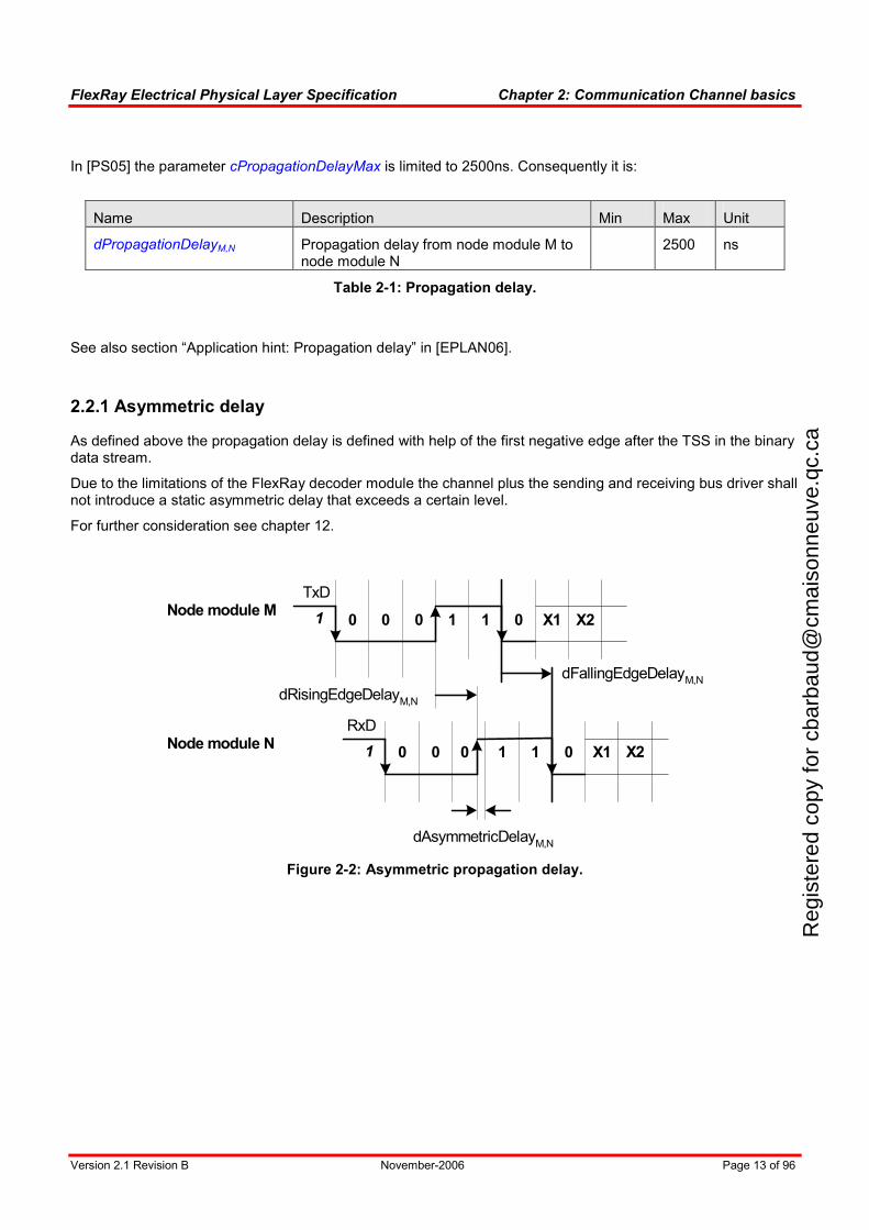
2.2.1 Asymmetric delay
As defined above the propagation delay is defined with help of the first negative edge after the TSS in the binary data stream.
Due to the limitations of the FlexRay decoder module the channel plus the sending and receiving bus driver shall not introduce a static asymmetric delay that exceeds a certain level.
For further consideration see chapter 12.
1 0 X1 X2
TxD
RxD
0 00
1 0 X100 X2
dFallingEdgeDelayM,N
Node module M
Node module N0
1
1
1
1
dRisingEdgeDelayM,N
dAsymmetricDelayM,N
Figure 2-2: Asymmetric propagation delay.
Reg
iste
red
copy
for
cbar
baud
@cm
aiso
nneu
ve.q
c.ca
FlexRay Electrical Physical Layer Specification Chapter 2: Communication Channel basics
Version 2.1 Revision B November-2006 Page 14 of 96
2.3 Truncation
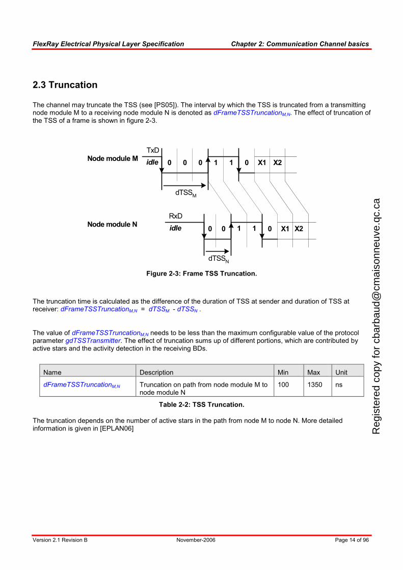
The channel may truncate the TSS (see [PS05]). The interval by which the TSS is truncated from a transmitting node module M to a receiving node module N is denoted as dFrameTSSTruncationM,N. The effect of truncation of the TSS of a frame is shown in figure 2-3.
Node module N
1 0 X1 X2
TxD
RxD
0 00
1 0 X100 X2
dTSSN
Node module Midle
idle
1
1
dTSSM
Figure 2-3: Frame TSS Truncation.
The truncation time is calculated as the difference of the duration of TSS at sender and duration of TSS at receiver: dFrameTSSTruncationM,N = dTSSM - dTSSN .
The value of dFrameTSSTruncationM,N needs to be less than the maximum configurable value of the protocol parameter gdTSSTransmitter. The effect of truncation sums up of different portions, which are contributed by active stars and the activity detection in the receiving BDs.
Name Description Min Max Unit
dFrameTSSTruncationM,N Truncation on path from node module M to node module N
100 1350 ns
Table 2-2: TSS Truncation.
The truncation depends on the number of active stars in the path from node M to node N. More detailed information is given in [EPLAN06] R
egis
tere
d co
py fo
r cb
arba
ud@
cmai
sonn
euve
.qc.
ca
FlexRay Electrical Physical Layer Specification Chapter 2: Communication Channel basics
Version 2.1 Revision B November-2006 Page 15 of 96
2.4 Symbol length change
Quite similar to the truncation of the TSS the length of symbols is changed while traveling through the physical layer. Besides the truncation at the beginning by the activity detection time a lengthening at the end by the idle detection time occurs. These effects are described in detail in section 8.9.4.
Name Description Min Max Unit
dSymbolLengthChangeM,N Change of length of a symbol on path from node module M to node module N
-1200 900 ns
A negative value means that the symbol is shortened, a positive value means the symbol is elongated.
Table 2-3: Symbol length change.
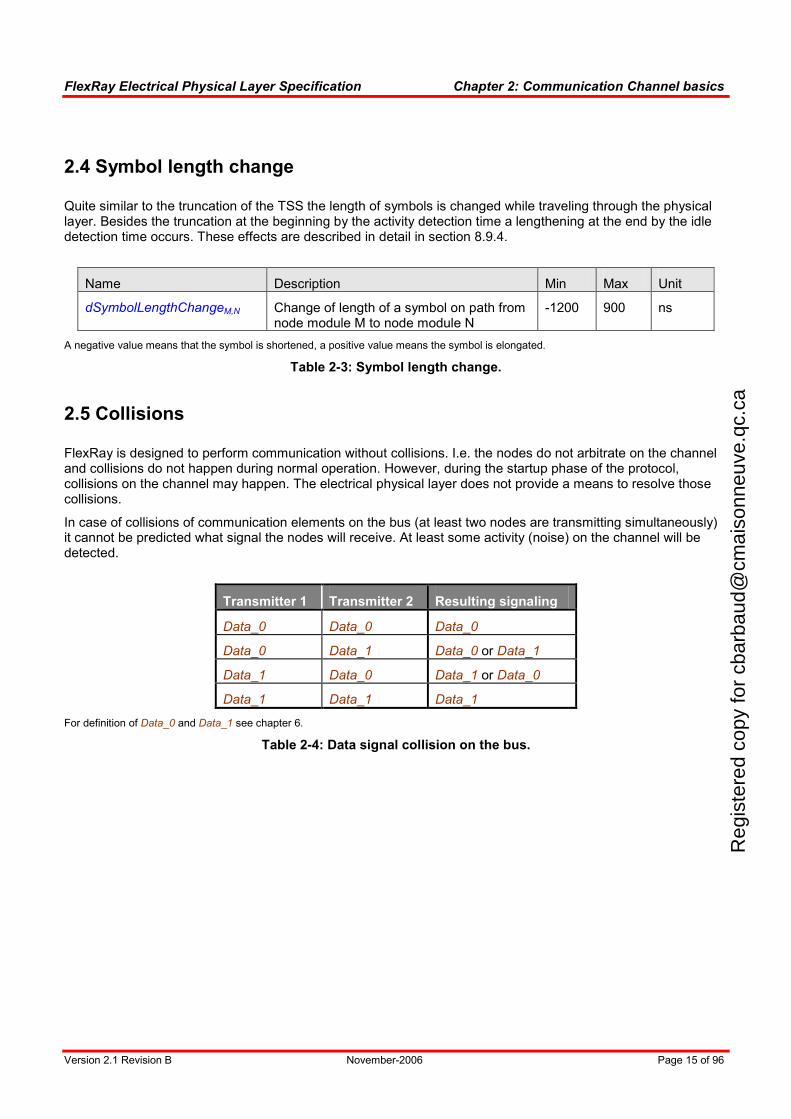
2.5 Collisions
FlexRay is designed to perform communication without collisions. I.e. the nodes do not arbitrate on the channel and collisions do not happen during normal operation. However, during the startup phase of the protocol, collisions on the channel may happen. The electrical physical layer does not provide a means to resolve those collisions.
In case of collisions of communication elements on the bus (at least two nodes are transmitting simultaneously) it cannot be predicted what signal the nodes will receive. At least some activity (noise) on the channel will be detected.
Transmitter 1 Transmitter 2 Resulting signaling
Data_0 Data_0 Data_0
Data_0 Data_1 Data_0 or Data_1
Data_1 Data_0 Data_1 or Data_0
Data_1 Data_1 Data_1
For definition of Data_0 and Data_1 see chapter 6.
Table 2-4: Data signal collision on the bus. R
egis
tere
d co
py fo
r cb
arba
ud@
cmai
sonn
euve
.qc.
ca
FlexRay Electrical Physical Layer Specification Chapter 2: Communication Channel basics
Version 2.1 Revision B November-2006 Page 16 of 96
2.6 EMC jitter
2.6.1 EMC jitter on signal edges
Jitter on signal edges, i.e. those edges that are different from first transition from HIGH to LOW at start of frame and the last transition from LOW to HIGH at the end of a frame, shall be considered in the course of system evaluation.
2.6.2 EMC jitter on TSS-truncation
Jitter on the TSS-truncation, which means jitter on the first falling edge in a frame, might shorten the TSS additionally to the truncation as described in section 2.3.
2.6.3 EMC jitter on Symbol length change
Jitter on the two edges of symbols might lead to deviations of the symbol length change as described in section 2.4.
Reg
iste
red
copy
for
cbar
baud
@cm
aiso
nneu
ve.q
c.ca
FlexRay Electrical Physical Layer Specification Chapter 2: Communication Channel basics
Version 2.1 Revision B November-2006 Page 17 of 96
2.7 Wake-up patterns
2.7.1 Overview
Independent from the data rate wake-up patterns can be sent to remotely wake nodes that are in Sleep mode.
2.7.2 Valid wake-up pattern
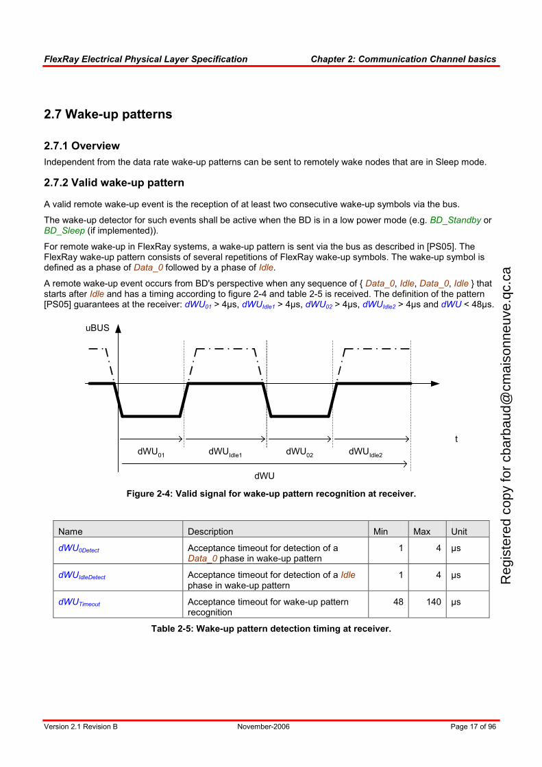
A valid remote wake-up event is the reception of at least two consecutive wake-up symbols via the bus.
The wake-up detector for such events shall be active when the BD is in a low power mode (e.g. BD_Standby or BD_Sleep (if implemented)).
For remote wake-up in FlexRay systems, a wake-up pattern is sent via the bus as described in [PS05]. The FlexRay wake-up pattern consists of several repetitions of FlexRay wake-up symbols. The wake-up symbol is defined as a phase of Data_0 followed by a phase of Idle.
A remote wake-up event occurs from BD's perspective when any sequence of Data_0, Idle, Data_0, Idle that starts after Idle and has a timing according to figure 2-4 and table 2-5 is received. The definition of the pattern [PS05] guarantees at the receiver: dWU01 > 4µs, dWUIdle1 > 4µs, dWU02 > 4µs, dWUIdle2 > 4µs and dWU < 48µs.
dWUIdle1
dWU
dWU01
dWU02
dWUIdle2
t
uBUS
Figure 2-4: Valid signal for wake-up pattern recognition at receiver.
Name Description Min Max Unit
dWU0Detect Acceptance timeout for detection of a Data_0 phase in wake-up pattern
1 4 µs
dWUIdleDetect Acceptance timeout for detection of a Idle phase in wake-up pattern
1 4 µs
dWUTimeout Acceptance timeout for wake-up pattern recognition
48 140 µs
Table 2-5: Wake-up pattern detection timing at receiver.
Reg
iste
red
copy
for
cbar
baud
@cm
aiso
nneu
ve.q
c.ca
FlexRay Electrical Physical Layer Specification Chapter 2: Communication Channel basics
Version 2.1 Revision B November-2006 Page 18 of 96
Short discontinuities (e.g. due to external disturbances like injection of RF fields) in Data_0 or Idle phases shall not harm the recognition of a remote wake-up, therefore uBus shall be evaluated after integrative filtering in order to achieve a sufficient robustness against such disturbances. The acceptable discontinuities depend on implementation and need to be specified on BD product level.
Moreover, the wake-up detector is allowed to judge Data_1 as Idle and the behavior needs to be specified on BD product level. Thus, the BD might also wake-up upon receiving other patterns, e.g. FlexRay frames.
Mind that idle and activity detection is the process how the wake-up pattern is received, see section 8.9.2 Receiver behavior and especially table 8-16.
2.7.3 Non valid wake-up patterns
The BD shall not wake-up, when
a) the first idle phase is shorter than 1µs, while the Data_0 phases are 6µs
b) the second Data_0 phase is shorter than 1µs, while the first Data_0 phase and the first idle phase are 6µs
c) the first idle phase is longer than 140µs, while the Data_0 phases are 6µs
Reg
iste
red
copy
for
cbar
baud
@cm
aiso
nneu
ve.q
c.ca
FlexRay Electrical Physical Layer Specification Chapter 3: Principle of FlexRay Networking
Version 2.1 Revision B November-2006 Page 19 of 96
Chapter 3 Principle of FlexRay Networking
3.1 Objective
This chapter shows the basic operation principle of FlexRay networks.
3.2 Interconnection of nodes
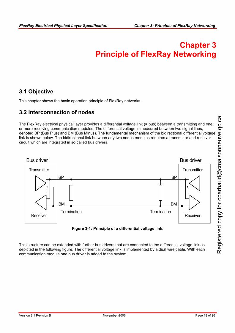
The FlexRay electrical physical layer provides a differential voltage link (= bus) between a transmitting and one or more receiving communication modules. The differential voltage is measured between two signal lines, denoted BP (Bus Plus) and BM (Bus Minus). The fundamental mechanism of the bidirectional differential voltage link is shown below. The bidirectional link between any two nodes modules requires a transmitter and receiver circuit which are integrated in so called bus drivers.
Termination
Transmitter
ReceiverTermination
Transmitter
Receiver
Bus driver Bus driver
BP
BM
BP
BM
Figure 3-1: Principle of a differential voltage link.
This structure can be extended with further bus drivers that are connected to the differential voltage link as depicted in the following figure. The differential voltage link is implemented by a dual wire cable. With each communication module one bus driver is added to the system.
Reg
iste
red
copy
for
cbar
baud
@cm
aiso
nneu
ve.q
c.ca
FlexRay Electrical Physical Layer Specification Chapter 3: Principle of FlexRay Networking
Version 2.1 Revision B November-2006 Page 20 of 96
Termination
Transmitter
ReceiverTermination
Transmitter
Receiver
Bus driver
Bus driver Bus driver
Bus driver
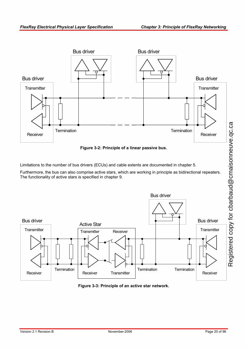
Figure 3-2: Principle of a linear passive bus.
Limitations to the number of bus drivers (ECUs) and cable extents are documented in chapter 5.
Furthermore, the bus can also comprise active stars, which are working in principle as bidirectional repeaters. The functionality of active stars is specified in chapter 9.
Termination
Transmitter
ReceiverTermination
Transmitter
Receiver
Transmitter
Receiver Transmitter
Receiver
Active StarBus driver
Bus driver
Bus driver
Termination
Figure 3-3: Principle of an active star network.
Reg
iste
red
copy
for
cbar
baud
@cm
aiso
nneu
ve.q
c.ca
FlexRay Electrical Physical Layer Specification Chapter 4: Network Components
Version 2.1 Revision B November-2006 Page 21 of 96
Chapter 4 Network Components
4.1 Objective
This chapter introduces some basic network components that are used to build up FlexRay networks.
4.2 Cables
The objective of this subsection is to specify the required cable characteristics, but not to define a selection of cable types. The medium in use for FlexRay busses may be unshielded as well as shielded cables, as long as they provide the following characteristics:
Name Description Min Max Unit
Z0 Differential mode impedance @ 10 MHz (*) 80 110 Ω
T’0 Specific line delay 10 ns / m
α5MHz Cable attenuation @ 5 MHz (sine wave) 82 dB / km
(*) see [EPLAN06]
Table 4-1: Cable characteristics.
4.3 Connectors
This specification does not prescribe certain connectors for FlexRay systems. However, any electrical connector used in FlexRay busses shall meet the following constraints:
Name Description Min Max Unit
RDCContact Contact resistance (including crimps) 50 mΩ
ZConnector Impedance of connector 70 200 Ω
lCoupling Length coupling connection (*) 150 mm
dContactInterruption (**) Contact resistance RDCContact > 1Ω 100 ns
(*) this parameter defines the length of the connectors including the termination areas of the cables (**) this requirement is to be generally understood as an quality issue and has no direct link with the timing performance of FlexRay.
Table 4-2: Connector parameters.
See further recommendations about connectors in [EPLAN06].
Reg
iste
red
copy
for
cbar
baud
@cm
aiso
nneu
ve.q
c.ca
FlexRay Electrical Physical Layer Specification Chapter 4: Network Components
Version 2.1 Revision B November-2006 Page 22 of 96
4.4 Cable termination
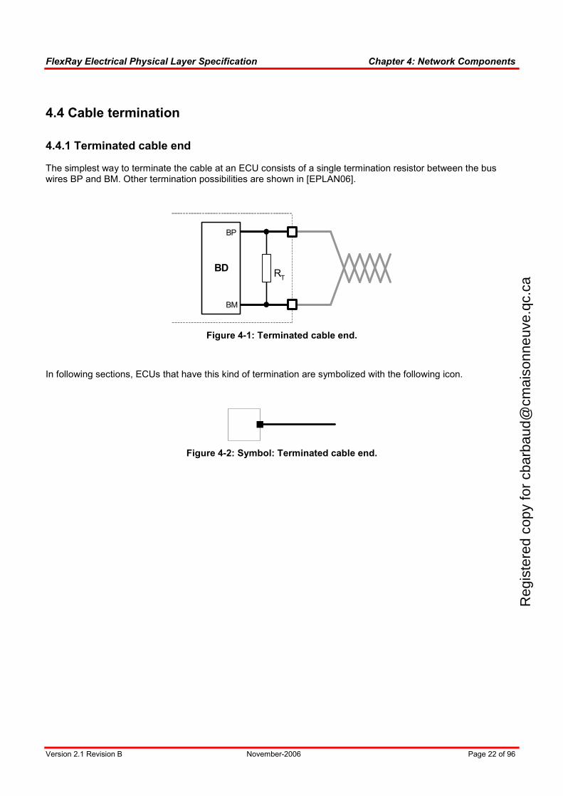
4.4.1 Terminated cable end
The simplest way to terminate the cable at an ECU consists of a single termination resistor between the bus wires BP and BM. Other termination possibilities are shown in [EPLAN06].
BD
BP
BM
RT
Figure 4-1: Terminated cable end.
In following sections, ECUs that have this kind of termination are symbolized with the following icon.
Figure 4-2: Symbol: Terminated cable end.
Reg
iste
red
copy
for
cbar
baud
@cm
aiso
nneu
ve.q
c.ca
FlexRay Electrical Physical Layer Specification Chapter 4: Network Components
Version 2.1 Revision B November-2006 Page 23 of 96
4.4.2 Un-terminated cable end
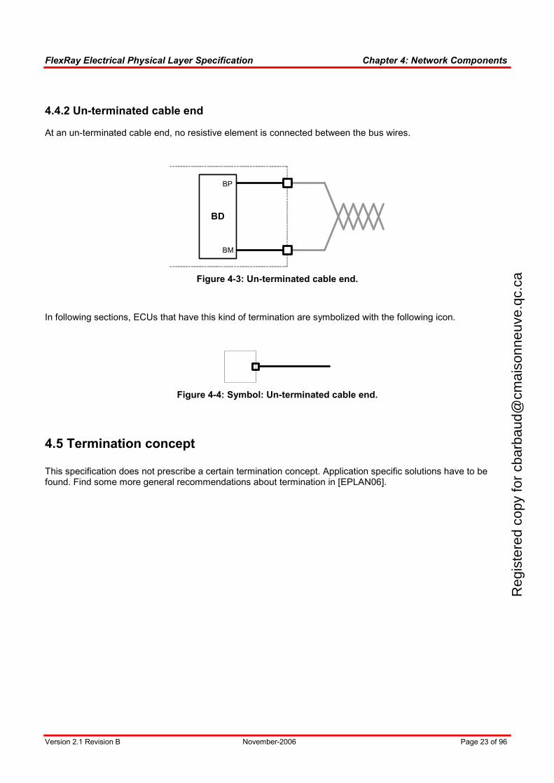
At an un-terminated cable end, no resistive element is connected between the bus wires.
BD
BP
BM
Figure 4-3: Un-terminated cable end.
In following sections, ECUs that have this kind of termination are symbolized with the following icon.
Figure 4-4: Symbol: Un-terminated cable end.
4.5 Termination concept
This specification does not prescribe a certain termination concept. Application specific solutions have to be found. Find some more general recommendations about termination in [EPLAN06].
Reg
iste
red
copy
for
cbar
baud
@cm
aiso
nneu
ve.q
c.ca
FlexRay Electrical Physical Layer Specification Chapter 4: Network Components
Version 2.1 Revision B November-2006 Page 24 of 96
4.6 Common mode chokes
This specification does not prescribe a certain common mode choke for FlexRay systems. However, any common mode choke used in FlexRay systems shall meet the following constraints over the entire temperature range as specified in section 11.5:
Name Description Min Max Unit
RCMC Resistance (per line) 2 Ω
Table 4-3: Common mode choke parameters.
See further recommendations about common mode chokes in [EPLAN06].
4.7 DC bus load
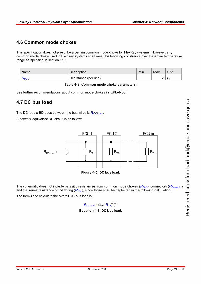
The DC load a BD sees between the bus wires is RDCLoad.
A network equivalent DC circuit is as follows:
RT1
ECU 1
RDCLoad
RT2
ECU 2
RTm
ECU m
Figure 4-5: DC bus load.
The schematic does not include parasitic resistances from common mode chokes (RCMC), connectors (RConnector) and the series resistance of the wiring (RWire), since those shall be neglected in the following calculation:
The formula to calculate the overall DC bus load is:
RDCLoad = (Σm (RTm)-1
)-1
Equation 4-1: DC bus load.
Reg
iste
red
copy
for
cbar
baud
@cm
aiso
nneu
ve.q
c.ca
FlexRay Electrical Physical Layer Specification Chapter 4: Network Components
Version 2.1 Revision B November-2006 Page 25 of 96
Name Description Min Max Unit
RDCLoad DC bus load 40 55 Ω
Table 4-4: DC bus load limitation.
Mind that the termination resistance RTm is usually a termination resistor in parallel to the BD’s receiver common mode input resistance (see section 8.9.1). The termination resistor might also be applied outside the ECU, e.g. at a network splice. In case of an un-terminated cable end according to section 4.3.2. the resistance RTm represents only the BD’s receiver common mode input resistance.
Some exemplary termination concepts for different bus structures are described in [EPLAN06]. All termination concepts have to consider the DC bus load limitation as defined here.
Reg
iste
red
copy
for
cbar
baud
@cm
aiso
nneu
ve.q
c.ca
FlexRay Electrical Physical Layer Specification Chapter 5: Network Topology
Version 2.1 Revision B November-2006 Page 26 of 96
Chapter 5 Network Topology
5.1 Objective
This chapter introduces possible bus structures, their names and parameters. The layout of busses has to follow the constraints that are explained in this chapter. Application examples and recommendations are given in [EPLAN06].
Dual channel applications, a main feature of FlexRay, are discussed at the end of this chapter.
All FlexRay topologies are 'linear', which means that they are free from rings or closed loops respectively.
A termination concept has to be found for each topology implementation individually. General hints can be found in [EPLAN06]. Whether a topology/termination combination composes a valid FlexRay network has to be judged according the signal integrity requirements as given in chapter 7.
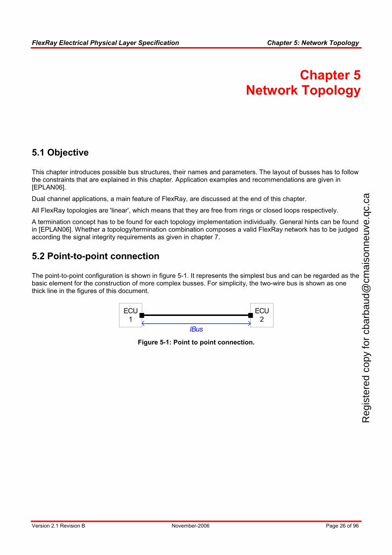
5.2 Point-to-point connection
The point-to-point configuration is shown in figure 5-1. It represents the simplest bus and can be regarded as the basic element for the construction of more complex busses. For simplicity, the two-wire bus is shown as one thick line in the figures of this document.
lBus
ECU
2
ECU
1
Figure 5-1: Point to point connection.
Reg
iste
red
copy
for
cbar
baud
@cm
aiso
nneu
ve.q
c.ca
FlexRay Electrical Physical Layer Specification Chapter 5: Network Topology
Version 2.1 Revision B November-2006 Page 27 of 96
5.3 Passive star
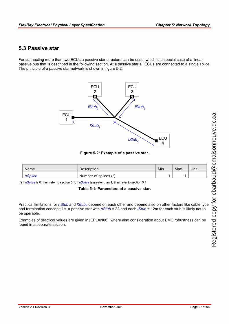
For connecting more than two ECUs a passive star structure can be used, which is a special case of a linear passive bus that is described in the following section. At a passive star all ECUs are connected to a single splice. The principle of a passive star network is shown in figure 5-2.
lStub1
lStub3
lStub4
ECU
1
ECU
3
ECU
2
ECU
4
lStub2
Figure 5-2: Example of a passive star.
Name Description Min Max Unit
nSplice Number of splices (*) 1 1
(*) if nSplice is 0, then refer to section 5.1, if nSplice is greater than 1, then refer to section 5.4
Table 5-1: Parameters of a passive star.
Practical limitations for nStub and lStubN depend on each other and depend also on other factors like cable type and termination concept; i.e. a passive star with nStub = 22 and each lStub = 12m for each stub is likely not to be operable.
Examples of practical values are given in [EPLAN06], where also consideration about EMC robustness can be found in a separate section.
Reg
iste
red
copy
for
cbar
baud
@cm
aiso
nneu
ve.q
c.ca
FlexRay Electrical Physical Layer Specification Chapter 5: Network Topology
Version 2.1 Revision B November-2006 Page 28 of 96
5.4 Linear passive bus
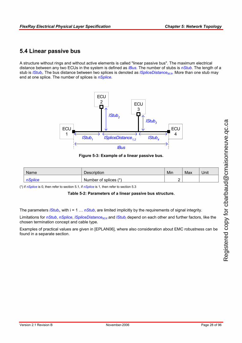
A structure without rings and without active elements is called "linear passive bus". The maximum electrical distance between any two ECUs in the system is defined as lBus. The number of stubs is nStub. The length of a stub is lStubi. The bus distance between two splices is denoted as lSpliceDistanceM,N. More than one stub may end at one splice. The number of splices is nSplice.
lBus
lSpliceDistance1,2
lStub2
ECU
4
ECU
1
ECU
2ECU
3
lStub1
lStub3
lStub4
Figure 5-3: Example of a linear passive bus.
Name Description Min Max Unit
nSplice Number of splices (*) 2
(*) if nSplice is 0, then refer to section 5.1, if nSplice is 1, then refer to section 5.3
Table 5-2: Parameters of a linear passive bus structure.
The parameters lStubi, with i = 1 … nStub, are limited implicitly by the requirements of signal integrity.
Limitations for nStub, nSplice, lSpliceDistanceM,N and lStubi depend on each other and further factors, like the chosen termination concept and cable type.
Examples of practical values are given in [EPLAN06], where also consideration about EMC robustness can be found in a separate section.
Reg
iste
red
copy
for
cbar
baud
@cm
aiso
nneu
ve.q
c.ca
FlexRay Electrical Physical Layer Specification Chapter 5: Network Topology
Version 2.1 Revision B November-2006 Page 29 of 96
5.5 Active star network
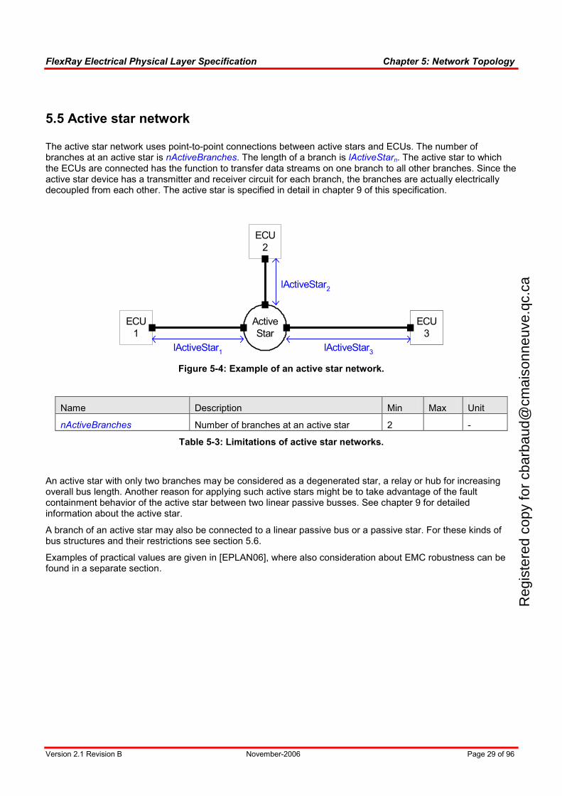
The active star network uses point-to-point connections between active stars and ECUs. The number of branches at an active star is nActiveBranches. The length of a branch is lActiveStarn. The active star to which the ECUs are connected has the function to transfer data streams on one branch to all other branches. Since the active star device has a transmitter and receiver circuit for each branch, the branches are actually electrically decoupled from each other. The active star is specified in detail in chapter 9 of this specification.
Active
Star
ECU
1
ECU
3
ECU
2
lActiveStar1
lActiveStar2
lActiveStar3
Figure 5-4: Example of an active star network.
Name Description Min Max Unit
nActiveBranches Number of branches at an active star 2 -
Table 5-3: Limitations of active star networks.
An active star with only two branches may be considered as a degenerated star, a relay or hub for increasing overall bus length. Another reason for applying such active stars might be to take advantage of the fault containment behavior of the active star between two linear passive busses. See chapter 9 for detailed information about the active star.
A branch of an active star may also be connected to a linear passive bus or a passive star. For these kinds of bus structures and their restrictions see section 5.6.
Examples of practical values are given in [EPLAN06], where also consideration about EMC robustness can be found in a separate section.
Reg
iste
red
copy
for
cbar
baud
@cm
aiso
nneu
ve.q
c.ca
FlexRay Electrical Physical Layer Specification Chapter 5: Network Topology
Version 2.1 Revision B November-2006 Page 30 of 96
5.6 Cascaded active stars
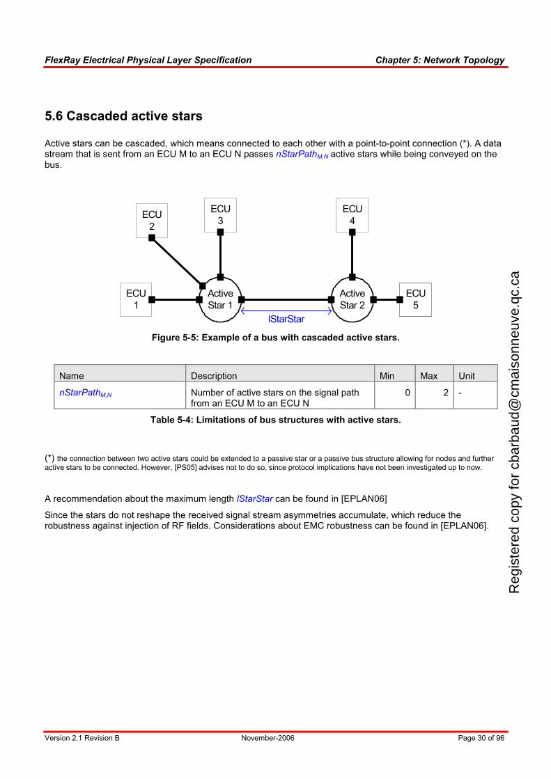
Active stars can be cascaded, which means connected to each other with a point-to-point connection (*). A data stream that is sent from an ECU M to an ECU N passes nStarPathM,N active stars while being conveyed on the bus.
Active
Star 1
Active
Star 2
ECU
1
ECU
5
ECU
2
ECU
4
ECU
3
lStarStar
Figure 5-5: Example of a bus with cascaded active stars.
Name Description Min Max Unit
nStarPathM,N Number of active stars on the signal path from an ECU M to an ECU N
0 2 -
Table 5-4: Limitations of bus structures with active stars.
(*) the connection between two active stars could be extended to a passive star or a passive bus structure allowing for nodes and further
active stars to be connected. However, [PS05] advises not to do so, since protocol implications have not been investigated up to now.
A recommendation about the maximum length lStarStar can be found in [EPLAN06]
Since the stars do not reshape the received signal stream asymmetries accumulate, which reduce the robustness against injection of RF fields. Considerations about EMC robustness can be found in [EPLAN06].
Reg
iste
red
copy
for
cbar
baud
@cm
aiso
nneu
ve.q
c.ca
FlexRay Electrical Physical Layer Specification Chapter 5: Network Topology
Version 2.1 Revision B November-2006 Page 31 of 96
5.7 Hybrid topologies
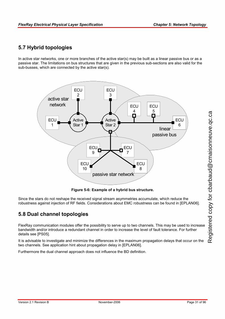
In active star networks, one or more branches of the active star(s) may be built as a linear passive bus or as a passive star. The limitations on bus structures that are given in the previous sub-sections are also valid for the sub-busses, which are connected by the active star(s).
Active
Star 2
ECU
1
ECU
5
ECU
2
ECU
3
ECU
4
ECU
6
passive star network
linear
passive bus
active star
network
Active
Star 1
ECU
10
ECU
7
ECU
8
ECU
9
Figure 5-6: Example of a hybrid bus structure.
Since the stars do not reshape the received signal stream asymmetries accumulate, which reduce the robustness against injection of RF fields. Considerations about EMC robustness can be found in [EPLAN06].
5.8 Dual channel topologies
FlexRay communication modules offer the possibility to serve up to two channels. This may be used to increase bandwidth and/or introduce a redundant channel in order to increase the level of fault tolerance. For further details see [PS05].
It is advisable to investigate and minimize the differences in the maximum propagation delays that occur on the two channels. See application hint about propagation delay in [EPLAN06].
Furthermore the dual channel approach does not influence the BD definition.
Reg
iste
red
copy
for
cbar
baud
@cm
aiso
nneu
ve.q
c.ca
FlexRay Electrical Physical Layer Specification Chapter 6: Electrical Signaling
Version 2.1 Revision B November-2006 Page 32 of 96
Chapter 6 Electrical Signaling
6.1 Objective
This chapter defines the analog electrical signals on the FlexRay bus wires.
6.2 Overview
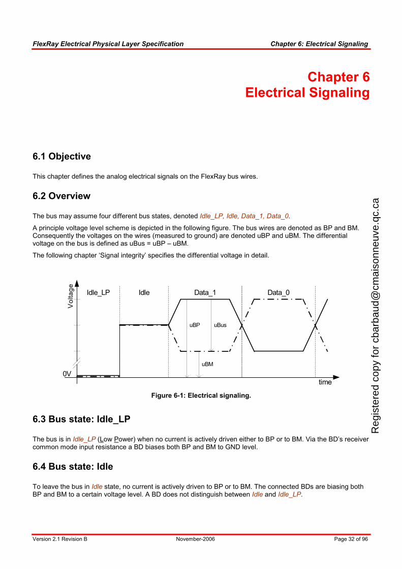
The bus may assume four different bus states, denoted Idle_LP, Idle, Data_1, Data_0.
A principle voltage level scheme is depicted in the following figure. The bus wires are denoted as BP and BM. Consequently the voltages on the wires (measured to ground) are denoted uBP and uBM. The differential voltage on the bus is defined as uBus = uBP – uBM.
The following chapter ‘Signal integrity’ specifies the differential voltage in detail.
time
uBM
uBP uBus
Idle_LP Idle Data_1 Data_0
0V
Vo
lta
ge
Figure 6-1: Electrical signaling.
6.3 Bus state: Idle_LP
The bus is in Idle_LP (Low Power) when no current is actively driven either to BP or to BM. Via the BD’s receiver common mode input resistance a BD biases both BP and BM to GND level.
6.4 Bus state: Idle
To leave the bus in Idle state, no current is actively driven to BP or to BM. The connected BDs are biasing both BP and BM to a certain voltage level. A BD does not distinguish between Idle and Idle_LP.
Reg
iste
red
copy
for
cbar
baud
@cm
aiso
nneu
ve.q
c.ca
FlexRay Electrical Physical Layer Specification Chapter 6: Electrical Signaling
Version 2.1 Revision B November-2006 Page 33 of 96
6.5 Bus state: Data_1
To drive the bus to Data_1 at least one BD forces a positive differential voltage between BP and BM.
6.6 Bus state: Data_0
To drive the bus to Data_0 at least one BD forces a negative differential voltage between BP and BM.
Reg
iste
red
copy
for
cbar
baud
@cm
aiso
nneu
ve.q
c.ca
FlexRay Electrical Physical Layer Specification Chapter 7: Signal integrity
Version 2.1 Revision B November-2006 Page 34 of 96
Chapter 7 Signal integrity
7.1 Objective
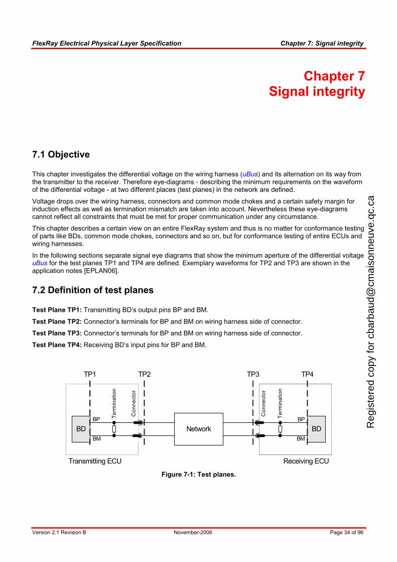
This chapter investigates the differential voltage on the wiring harness (uBus) and its alternation on its way from the transmitter to the receiver. Therefore eye-diagrams - describing the minimum requirements on the waveform of the differential voltage - at two different places (test planes) in the network are defined.
Voltage drops over the wiring harness, connectors and common mode chokes and a certain safety margin for induction effects as well as termination mismatch are taken into account. Nevertheless these eye-diagrams cannot reflect all constraints that must be met for proper communication under any circumstance.
This chapter describes a certain view on an entire FlexRay system and thus is no matter for conformance testing of parts like BDs, common mode chokes, connectors and so on, but for conformance testing of entire ECUs and wiring harnesses.
In the following sections separate signal eye diagrams that show the minimum aperture of the differential voltage uBus for the test planes TP1 and TP4 are defined. Exemplary waveforms for TP2 and TP3 are shown in the application notes [EPLAN06].
7.2 Definition of test planes
Test Plane TP1: Transmitting BD’s output pins BP and BM.
Test Plane TP2: Connector’s terminals for BP and BM on wiring harness side of connector.
Test Plane TP3: Connector’s terminals for BP and BM on wiring harness side of connector.
Test Plane TP4: Receiving BD’s input pins for BP and BM.
TP2
Transmitting ECU Receiving ECU
NetworkBD
TP3TP1
BD
TP4
BP
BM
BP
BM
Te
rmin
atio
n
Co
nn
ecto
r
Co
nn
ecto
r
Te
rmin
atio
n
Figure 7-1: Test planes.
Reg
iste
red
copy
for
cbar
baud
@cm
aiso
nneu
ve.q
c.ca
FlexRay Electrical Physical Layer Specification Chapter 7: Signal integrity
Version 2.1 Revision B November-2006 Page 35 of 96
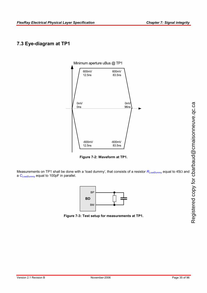
7.3 Eye-diagram at TP1
0mV
96ns
600mV
83.5ns
-600mV
83.5ns
600mV
12.5ns
0mV
0ns
-600mV
12.5ns
Minimum aperture uBus @ TP1
Figure 7-2: Waveform at TP1.
Measurements on TP1 shall be done with a ‘load dummy’, that consists of a resistor RLoadDummy equal to 45Ω and a CLoadDummy equal to 100pF in parallel.
BD
BP
BM
Figure 7-3: Test setup for measurements at TP1.
Reg
iste
red
copy
for
cbar
baud
@cm
aiso
nneu
ve.q
c.ca
FlexRay Electrical Physical Layer Specification Chapter 7: Signal integrity
Version 2.1 Revision B November-2006 Page 36 of 96
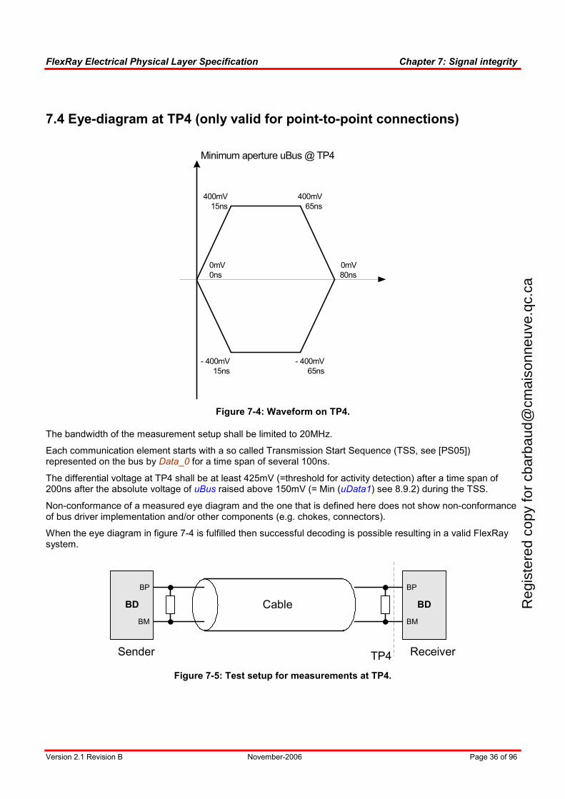
7.4 Eye-diagram at TP4 (only valid for point-to-point connections)
0mV
80ns
Minimum aperture uBus @ TP4
- 400mV
15ns
0mV
0ns
- 400mV
65ns
400mV
15ns
400mV
65ns
Figure 7-4: Waveform on TP4.
The bandwidth of the measurement setup shall be limited to 20MHz.
Each communication element starts with a so called Transmission Start Sequence (TSS, see [PS05]) represented on the bus by Data_0 for a time span of several 100ns.
The differential voltage at TP4 shall be at least 425mV (=threshold for activity detection) after a time span of 200ns after the absolute voltage of uBus raised above 150mV (= Min (uData1) see 8.9.2) during the TSS.
Non-conformance of a measured eye diagram and the one that is defined here does not show non-conformance of bus driver implementation and/or other components (e.g. chokes, connectors).
When the eye diagram in figure 7-4 is fulfilled then successful decoding is possible resulting in a valid FlexRay system.
BD
BP
BM
BD
BP
BM
Cable
TP4Sender Receiver
Figure 7-5: Test setup for measurements at TP4.
Reg
iste
red
copy
for
cbar
baud
@cm
aiso
nneu
ve.q
c.ca
FlexRay Electrical Physical Layer Specification Chapter 8: Electrical Bus Driver
Version 2.1 Revision B November-2006 Page 37 of 96
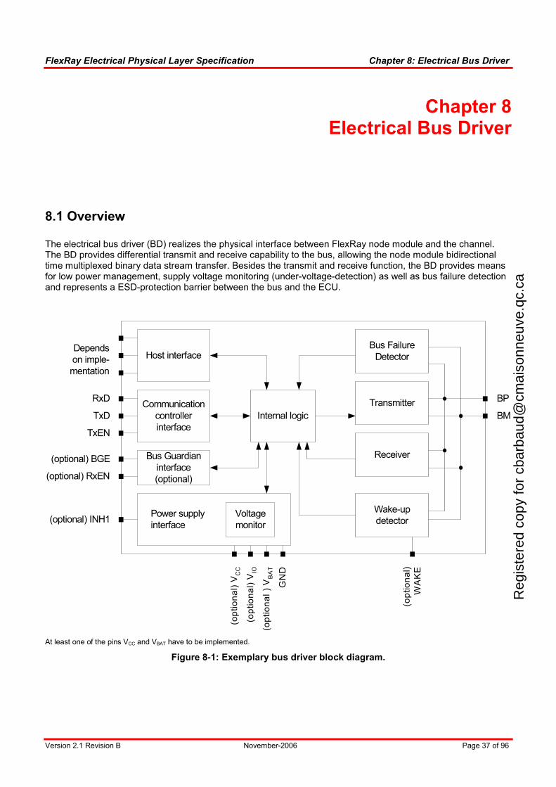
Chapter 8 Electrical Bus Driver
8.1 Overview
The electrical bus driver (BD) realizes the physical interface between FlexRay node module and the channel. The BD provides differential transmit and receive capability to the bus, allowing the node module bidirectional time multiplexed binary data stream transfer. Besides the transmit and receive function, the BD provides means for low power management, supply voltage monitoring (under-voltage-detection) as well as bus failure detection and represents a ESD-protection barrier between the bus and the ECU.
Transmitter
Receiver
Wake-up
detector
Host interface
Communication
controller
interface
Power supply
interface
Bus Guardian
interface
(optional)
Internal logic
Bus Failure
Detector
BP
BM
(optional) INH1
(optional) BGE
TxEN
TxD
RxD
(optional) RxEN
Depends
on imple-
mentation
(op
tio
na
l) V
CC
(op
tio
na
l) V
IO
(op
tio
na
l )
VB
AT
GN
D
(op
tio
na
l)
WA
KE
Voltage
monitor
At least one of the pins VCC and VBAT have to be implemented.
Figure 8-1: Exemplary bus driver block diagram.
Reg
iste
red
copy
for
cbar
baud
@cm
aiso
nneu
ve.q
c.ca
FlexRay Electrical Physical Layer Specification Chapter 8: Electrical Bus Driver
Version 2.1 Revision B November-2006 Page 38 of 96
8.2 Operation modes
The electrical BD supports a set of operation modes, which are described in this section. The operation modes BD_Normal and BD_Standby are mandatory to implement. Two optional modes are described and further product specific modes may be supported.
8.2.1 BD_Normal mode
The BD is able to send and receive data streams on the bus.
Not_Sleep is signaled on INH1 in case this interface is present, see section 8.7.1.
The bus wires are biased - see table 8-14 in section 8.9.1.
8.2.2 BD_Standby mode
The BD_Standby mode is a low power mode.
The BD is not able to send or receive data streams to/from the bus.
The BD could be able to detect wakeup events (optional, see 8.11).
The power consumption is reduced compared to BD_Normal.
Not_Sleep is signaled on INH1 in case this interface is present, see section 8.7.1.
The bus wires are terminated to GND via receiver common mode input resistance.
8.2.3 BD_Sleep mode (optional)
This option belongs to the functional class “BD voltage regulator control”, see section 8.18.1
The BD_Sleep mode is a low power mode.
The BD is not able to send or receive data streams to/from the bus.
The BD’s wake-up monitoring functions are operational.
The power consumption is reduced compared to BD_Normal.
Sleep is signaled on INH1.
The bus wires are terminated to GND via receiver common mode input resistance.
8.2.4 BD_ReceiveOnly mode (optional)
The BD is able to receive data streams on the bus, but not able to transmit.
Not_Sleep is signaled on INH1 in case this interface is present.
The bus wires are biased - see table 8-14 in section 8.9.1.
Reg
iste
red
copy
for
cbar
baud
@cm
aiso
nneu
ve.q
c.ca
FlexRay Electrical Physical Layer Specification Chapter 8: Electrical Bus Driver
Version 2.1 Revision B November-2006 Page 39 of 96
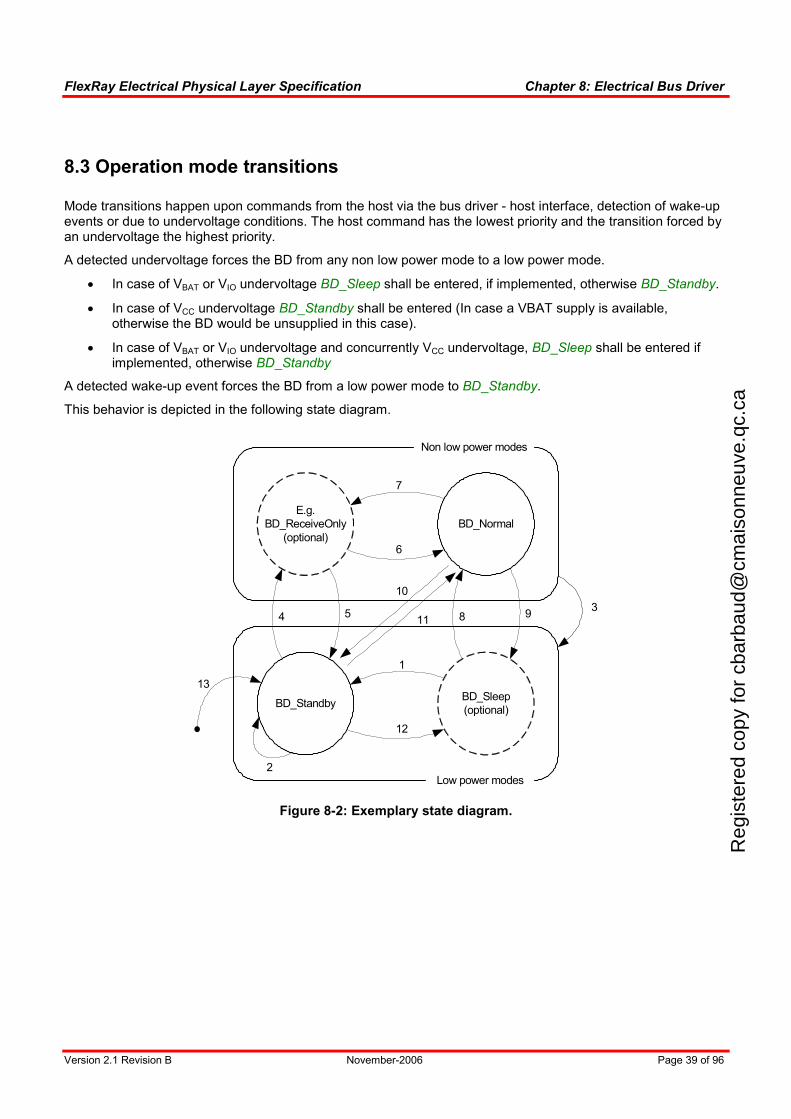
8.3 Operation mode transitions
Mode transitions happen upon commands from the host via the bus driver - host interface, detection of wake-up events or due to undervoltage conditions. The host command has the lowest priority and the transition forced by an undervoltage the highest priority.
A detected undervoltage forces the BD from any non low power mode to a low power mode.
• In case of VBAT or VIO undervoltage BD_Sleep shall be entered, if implemented, otherwise BD_Standby.
• In case of VCC undervoltage BD_Standby shall be entered (In case a VBAT supply is available, otherwise the BD would be unsupplied in this case).
• In case of VBAT or VIO undervoltage and concurrently VCC undervoltage, BD_Sleep shall be entered if implemented, otherwise BD_Standby
A detected wake-up event forces the BD from a low power mode to BD_Standby.
This behavior is depicted in the following state diagram.
BD_Normal
BD_StandbyBD_Sleep
(optional)
Low power modes
Non low power modes
E.g.
BD_ReceiveOnly
(optional)
1
12
4 5
7
6
8 93
10
11
2
13
Figure 8-2: Exemplary state diagram.
Reg
iste
red
copy
for
cbar
baud
@cm
aiso
nneu
ve.q
c.ca
FlexRay Electrical Physical Layer Specification Chapter 8: Electrical Bus Driver
Version 2.1 Revision B November-2006 Page 40 of 96
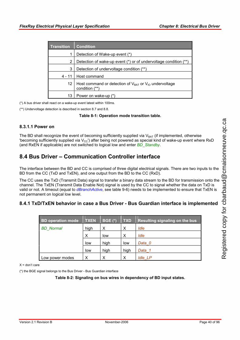
Transition Condition
1 Detection of Wake-up event (*)
2 Detection of wake-up event (*) or of undervoltage condition (**)
3 Detection of undervoltage condition (**)
4 - 11 Host command
12 Host command or detection of VBAT or VIO undervoltage condition (**)
13 Power on wake-up (*)
(*) A bus driver shall react on a wake-up event latest within 100ms.
(**) Undervoltage detection is described in section 8.7 and 8.8.
Table 8-1: Operation mode transition table.
8.3.1.1 Power on
The BD shall recognize the event of becoming sufficiently supplied via VBAT (if implemented, otherwise 'becoming sufficiently supplied via VCC') after being not powered as special kind of wake-up event where RxD (and RxEN if applicable) are not switched to logical low and enter BD_Standby.
8.4 Bus Driver – Communication Controller interface
The interface between the BD and CC is comprised of three digital electrical signals. There are two inputs to the BD from the CC (TxD and TxEN), and one output from the BD to the CC (RxD).
The CC uses the TxD (Transmit Data) signal to transfer a binary data stream to the BD for transmission onto the channel. The TxEN (Transmit Data Enable Not) signal is used by the CC to signal whether the data on TxD is valid or not. A timeout (equal to dBranchActive, see table 9-6) needs to be implemented to ensure that TxEN is not permanent on logical low level.
8.4.1 TxD/TxEN behavior in case a Bus Driver - Bus Guardian interface is implemented
BD operation mode TXEN BGE (*) TXD Resulting signaling on the bus
high X X Idle
X low X Idle
low high low Data_0
BD_Normal
low high high Data_1
Low power modes X X X Idle_LP
X = don’t care
(*) the BGE signal belongs to the Bus Driver - Bus Guardian interface
Table 8-2: Signaling on bus wires in dependency of BD input states.
Reg
iste
red
copy
for
cbar
baud
@cm
aiso
nneu
ve.q
c.ca
FlexRay Electrical Physical Layer Specification Chapter 8: Electrical Bus Driver
Version 2.1 Revision B November-2006 Page 41 of 96
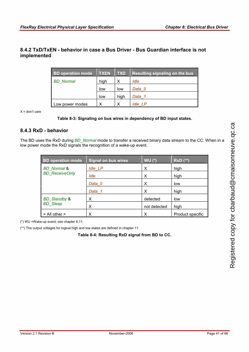
8.4.2 TxD/TxEN - behavior in case a Bus Driver - Bus Guardian interface is not implemented
BD operation mode TXEN TXD Resulting signaling on the bus
high X Idle
low low Data_0
BD_Normal
low high Data_1
Low power modes X X Idle_LP
X = don’t care
Table 8-3: Signaling on bus wires in dependency of BD input states.
8.4.3 RxD - behavior
The BD uses the RxD during BD_Normal mode to transfer a received binary data stream to the CC. When in a low power mode the RxD signals the recognition of a wake-up event.
BD operation mode Signal on bus wires WU (*) RxD (**)
Idle_LP X high
Idle X high
Data_0 X low
BD_Normal & BD_ReceiveOnly
Data_1 X high
X detected low BD_Standby & BD_Sleep
X not detected high
= All other = X X Product specific
(*) WU =Wake-up event; see chapter 8.11.
(**) The output voltages for logical high and low states are defined in chapter 11
Table 8-4: Resulting RxD signal from BD to CC.
Reg
iste
red
copy
for
cbar
baud
@cm
aiso
nneu
ve.q
c.ca
FlexRay Electrical Physical Layer Specification Chapter 8: Electrical Bus Driver
Version 2.1 Revision B November-2006 Page 42 of 96
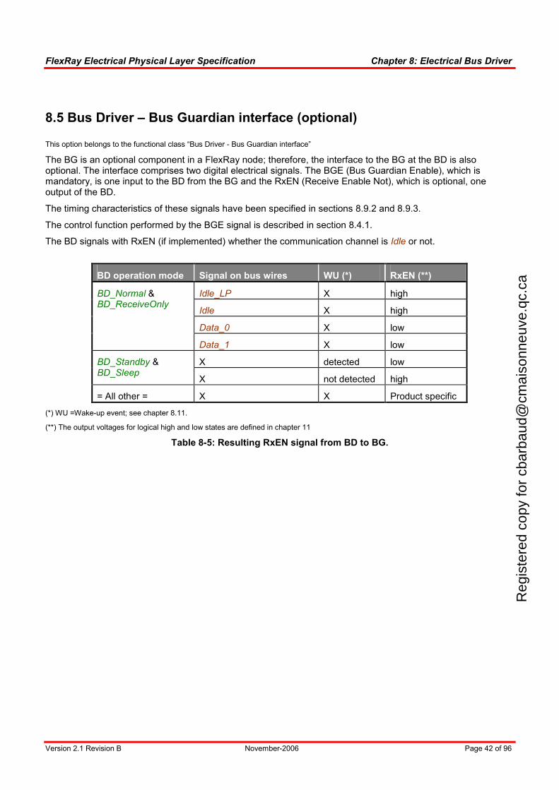
8.5 Bus Driver – Bus Guardian interface (optional)
This option belongs to the functional class “Bus Driver - Bus Guardian interface”
The BG is an optional component in a FlexRay node; therefore, the interface to the BG at the BD is also optional. The interface comprises two digital electrical signals. The BGE (Bus Guardian Enable), which is mandatory, is one input to the BD from the BG and the RxEN (Receive Enable Not), which is optional, one output of the BD.
The timing characteristics of these signals have been specified in sections 8.9.2 and 8.9.3.
The control function performed by the BGE signal is described in section 8.4.1.
The BD signals with RxEN (if implemented) whether the communication channel is Idle or not.
BD operation mode Signal on bus wires WU (*) RxEN (**)
Idle_LP X high
Idle X high
Data_0 X low
BD_Normal & BD_ReceiveOnly
Data_1 X low
X detected low BD_Standby & BD_Sleep
X not detected high
= All other = X X Product specific
(*) WU =Wake-up event; see chapter 8.11.
(**) The output voltages for logical high and low states are defined in chapter 11
Table 8-5: Resulting RxEN signal from BD to BG.
Reg
iste
red
copy
for
cbar
baud
@cm
aiso
nneu
ve.q
c.ca
FlexRay Electrical Physical Layer Specification Chapter 8: Electrical Bus Driver
Version 2.1 Revision B November-2006 Page 43 of 96
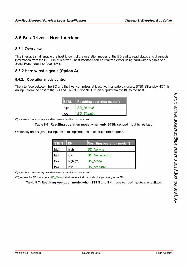
8.6 Bus Driver – Host interface
8.6.1 Overview
This interface shall enable the host to control the operation modes of the BD and to read status and diagnosis information from the BD. The bus driver – host interface can be realized either using hard-wired signals or a Serial Peripheral Interface (SPI).
8.6.2 Hard wired signals (Option A)
8.6.2.1 Operation mode control
The interface between the BD and the host comprises at least two mandatory signals. STBN (Standby NOT) is an input from the host to the BD and ERRN (Error NOT) is an output from the BD to the host.
STBN Resulting operation mode(*)
high BD_Normal
low BD_Standby
(*) in case no undervoltage conditions overrules the host command
Table 8-6: Resulting operation mode, when only STBN control input is realized.
Optionally an EN (Enable) input can be implemented to control further modes.
STBN EN Resulting operation mode(*)
high high BD_Normal
high low BD_ReceiveOnly
low high (**) BD_Sleep
low low BD_Standby
(*) in case no undervoltage conditions overrules the host command
(**) In case the BD has entered BD_Sleep it shall not react with a mode change on edges on EN
Table 8-7: Resulting operation mode, when STBN and EN mode control inputs are realized.
Reg
iste
red
copy
for
cbar
baud
@cm
aiso
nneu
ve.q
c.ca
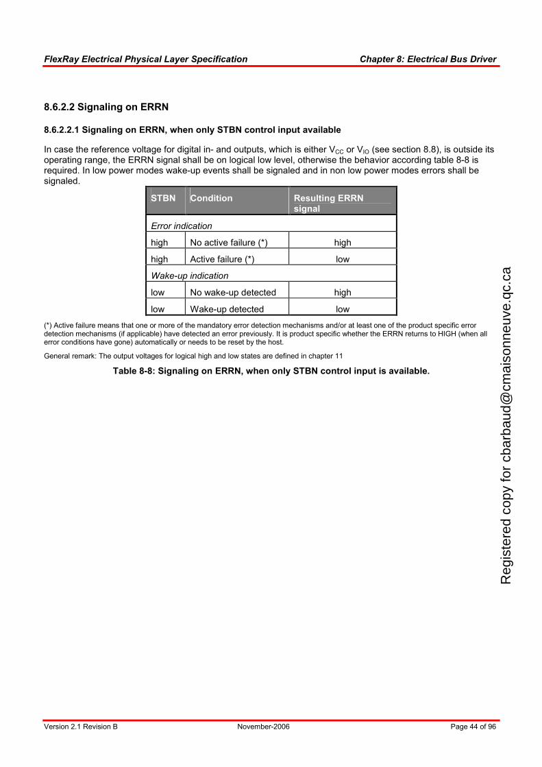
FlexRay Electrical Physical Layer Specification Chapter 8: Electrical Bus Driver
Version 2.1 Revision B November-2006 Page 44 of 96
8.6.2.2 Signaling on ERRN
8.6.2.2.1 Signaling on ERRN, when only STBN control input available
In case the reference voltage for digital in- and outputs, which is either VCC or VIO (see section 8.8), is outside its operating range, the ERRN signal shall be on logical low level, otherwise the behavior according table 8-8 is required. In low power modes wake-up events shall be signaled and in non low power modes errors shall be signaled.
STBN Condition Resulting ERRN signal
Error indication
high No active failure (*) high
high Active failure (*) low
Wake-up indication
low No wake-up detected high
low Wake-up detected low
(*) Active failure means that one or more of the mandatory error detection mechanisms and/or at least one of the product specific error detection mechanisms (if applicable) have detected an error previously. It is product specific whether the ERRN returns to HIGH (when all error conditions have gone) automatically or needs to be reset by the host.
General remark: The output voltages for logical high and low states are defined in chapter 11
Table 8-8: Signaling on ERRN, when only STBN control input is available.
Reg
iste
red
copy
for
cbar
baud
@cm
aiso
nneu
ve.q
c.ca
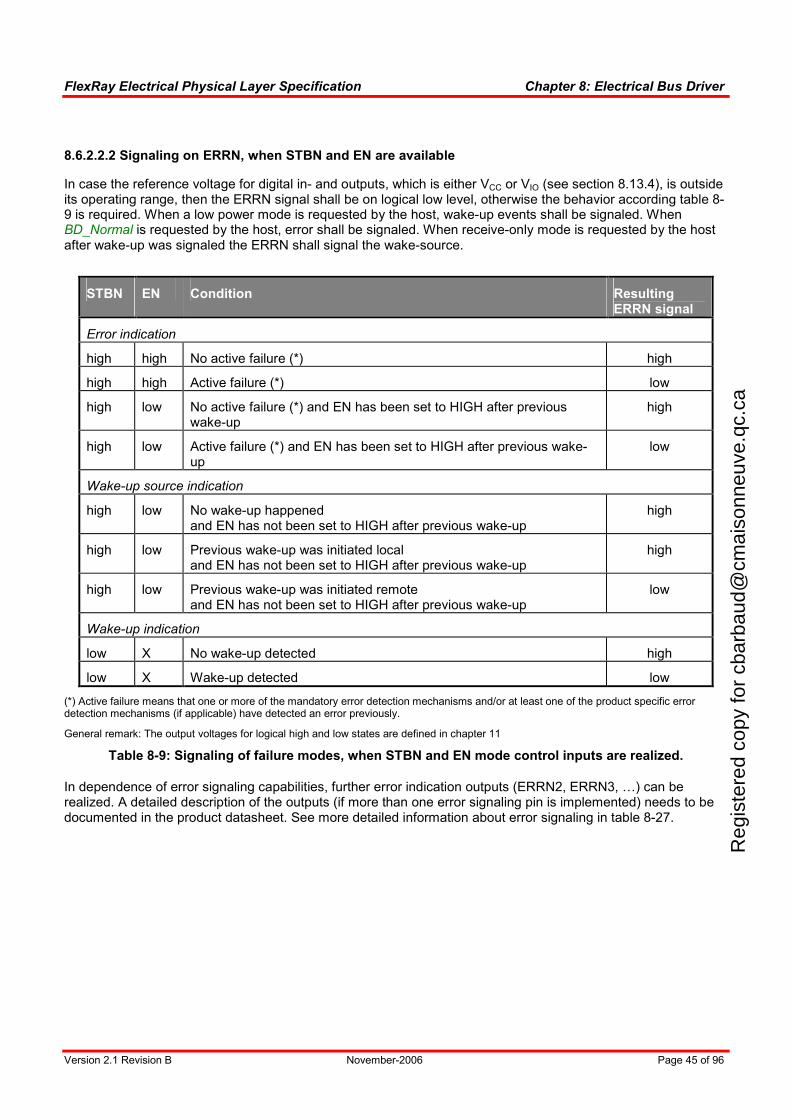
FlexRay Electrical Physical Layer Specification Chapter 8: Electrical Bus Driver
Version 2.1 Revision B November-2006 Page 45 of 96
8.6.2.2.2 Signaling on ERRN, when STBN and EN are available
In case the reference voltage for digital in- and outputs, which is either VCC or VIO (see section 8.13.4), is outside its operating range, then the ERRN signal shall be on logical low level, otherwise the behavior according table 8-9 is required. When a low power mode is requested by the host, wake-up events shall be signaled. When BD_Normal is requested by the host, error shall be signaled. When receive-only mode is requested by the host after wake-up was signaled the ERRN shall signal the wake-source.
STBN EN Condition Resulting ERRN signal
Error indication
high high No active failure (*) high
high high Active failure (*) low
high low No active failure (*) and EN has been set to HIGH after previous wake-up
high
high low Active failure (*) and EN has been set to HIGH after previous wake-up
low
Wake-up source indication
high low No wake-up happened and EN has not been set to HIGH after previous wake-up
high
high low Previous wake-up was initiated local and EN has not been set to HIGH after previous wake-up
high
high low Previous wake-up was initiated remote and EN has not been set to HIGH after previous wake-up
low
Wake-up indication
low X No wake-up detected high
low X Wake-up detected low
(*) Active failure means that one or more of the mandatory error detection mechanisms and/or at least one of the product specific error detection mechanisms (if applicable) have detected an error previously.
General remark: The output voltages for logical high and low states are defined in chapter 11
Table 8-9: Signaling of failure modes, when STBN and EN mode control inputs are realized.
In dependence of error signaling capabilities, further error indication outputs (ERRN2, ERRN3, …) can be realized. A detailed description of the outputs (if more than one error signaling pin is implemented) needs to be documented in the product datasheet. See more detailed information about error signaling in table 8-27.
Reg
iste
red
copy
for
cbar
baud
@cm
aiso
nneu
ve.q
c.ca
FlexRay Electrical Physical Layer Specification Chapter 8: Electrical Bus Driver
Version 2.1 Revision B November-2006 Page 46 of 96
8.6.3 Serial Peripheral Interface (SPI) (Option B)
In case the interface between BD and the host comprises a serial peripheral interface, this interface shall meet the electrical characteristics as described in chapter 11 of this specification.
Additionally, the BD shall have an interrupt line. The signal name shall be INTN.
At a minimum, the BD shall signal an interrupt to the host upon the occurrence of errors.
The data provided at the SPI interface is product specific.
It shall be possible to command the BD into any of its operation modes and to learn about the error status via the SPI interface.
For testing purposes, there shall be a product specific method to force the BD into BD_Normal mode without sending any command via the SPI.
8.7 Bus Driver – Power supply interface
The interface between the bus driver and the power supply comprises at least two pins, which are the ground connection (GND) and a supply pin, either VCC or VBAT. Furthermore this interface may comprise an optional inhibit output (INH1); see section 8.13.
A power supply input “VCC“ may be implemented, which shall be connected to a low voltage supply with nominal 5V. The minimum and maximum allowable voltages on VCC are product specific.
A power supply input “VBAT“ may be implemented, which can be directly connected to the vehicle battery (e.g. nominal 42V) in order to supply the BD, when a VCC input is not available or not implemented. The minimum and maximum allowable voltages on VBAT are product specific.
At least one of these two power supply inputs has to be implemented.
Moreover, there are dependencies to the functional classes “BD voltage regulator control” and “BD internal voltage regulator”, see section 8.13.
When a VCC power supply is not implemented or no sufficient voltage is available on this input, then the BD shall be operable in low power modes when the voltage on VBAT is equal or greater than 7V.
In case a VCC power supply is not implemented, then the BD shall be operable in all operation modes when the voltage on VBAT is equal to or greater than 5.5V.
In case VCC and VBAT power supplies are implemented and a sufficient voltage on VCC is available, then the BD shall be operable in all operation modes when the voltage on VBAT is equal to or greater than 5.5V (**).
R
egis
tere
d co
py fo
r cb
arba
ud@
cmai
sonn
euve
.qc.
ca
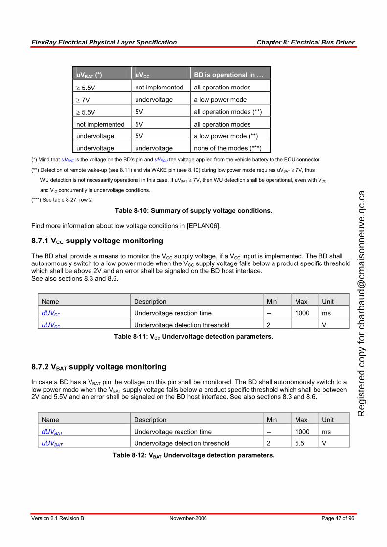
FlexRay Electrical Physical Layer Specification Chapter 8: Electrical Bus Driver
Version 2.1 Revision B November-2006 Page 47 of 96
uVBAT (*) uVCC BD is operational in …
≥ 5.5V not implemented all operation modes
≥ 7V undervoltage a low power mode
≥ 5.5V 5V all operation modes (**)
not implemented 5V all operation modes
undervoltage 5V a low power mode (**)
undervoltage undervoltage none of the modes (***)
(*) Mind that uVBAT is the voltage on the BD’s pin and uVECU the voltage applied from the vehicle battery to the ECU connector.
(**) Detection of remote wake-up (see 8.11) and via WAKE pin (see 8.10) during low power mode requires uVBAT ≥ 7V, thus
WU detection is not necessarily operational in this case. If uVBAT ≥ 7V, then WU detection shall be operational, even with VCC
and VIO concurrently in undervoltage conditions.
(***) See table 8-27, row 2
Table 8-10: Summary of supply voltage conditions.
Find more information about low voltage conditions in [EPLAN06].
8.7.1 VCC supply voltage monitoring
The BD shall provide a means to monitor the VCC supply voltage, if a VCC input is implemented. The BD shall autonomously switch to a low power mode when the VCC supply voltage falls below a product specific threshold which shall be above 2V and an error shall be signaled on the BD host interface. See also sections 8.3 and 8.6.
Name Description Min Max Unit
dUVCC Undervoltage reaction time -- 1000 ms
uUVCC Undervoltage detection threshold 2 V
Table 8-11: VCC Undervoltage detection parameters.
8.7.2 VBAT supply voltage monitoring
In case a BD has a VBAT pin the voltage on this pin shall be monitored. The BD shall autonomously switch to a low power mode when the VBAT supply voltage falls below a product specific threshold which shall be between 2V and 5.5V and an error shall be signaled on the BD host interface. See also sections 8.3 and 8.6.
Name Description Min Max Unit
dUVBAT Undervoltage reaction time -- 1000 ms
uUVBAT Undervoltage detection threshold 2 5.5 V
Table 8-12: VBAT Undervoltage detection parameters.
Reg
iste
red
copy
for
cbar
baud
@cm
aiso
nneu
ve.q
c.ca
FlexRay Electrical Physical Layer Specification Chapter 8: Electrical Bus Driver
Version 2.1 Revision B November-2006 Page 48 of 96
8.7.3 Inhibit output (optional)
This option belongs to the functional class “BD voltage regulator control”. This class comprises also the VBAT supply pin (see section 8.13.)
Optionally the bus driver - power supply interface may have an inhibit output signal (INH1) that is meant to control an external voltage regulator. The BD signals Sleep to the power supply, when leaving the INH1 pin floating and signals Not_Sleep, when driving the INH1 pin to uINH1 > uVBAT - 2V @ 100µA load, while uVBAT > 5.5V.
8.8 Bus Driver - Level shift interface (optional)
This option belongs to the functional class “BD logic level adaptation”
Optionally a “VIO“ voltage input can be implemented in order to apply a reference voltage for digital inputs and outputs. For more information, see chapter 11.
8.8.1 VIO voltage monitoring
In case there is a VIO voltage input implemented as reference for digital IO, the BD shall provide a means to monitor the VIO voltage. The BD shall autonomously switch to a low power mode when the VIO supply voltage falls below a product specific threshold which shall be above 0.75V and an error shall be signaled on the BD host interface. See also sections 8.3 and 8.6.
Name Description Min Max Unit
dUVIO Undervoltage reaction time -- 1000 ms
uUVIO Undervoltage detection threshold 0.75 V
Table 8-13: VIO Undervoltage detection parameters.
Reg
iste
red
copy
for
cbar
baud
@cm
aiso
nneu
ve.q
c.ca
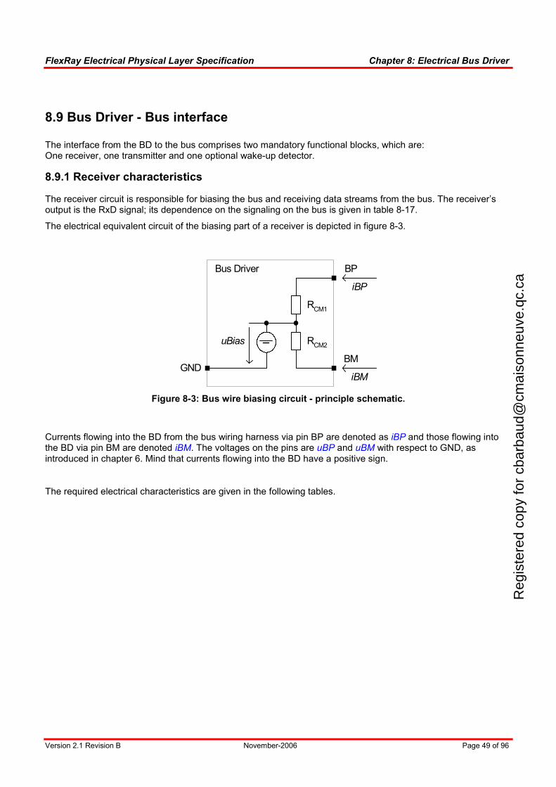
FlexRay Electrical Physical Layer Specification Chapter 8: Electrical Bus Driver
Version 2.1 Revision B November-2006 Page 49 of 96
8.9 Bus Driver - Bus interface
The interface from the BD to the bus comprises two mandatory functional blocks, which are: One receiver, one transmitter and one optional wake-up detector.
8.9.1 Receiver characteristics
The receiver circuit is responsible for biasing the bus and receiving data streams from the bus. The receiver’s output is the RxD signal; its dependence on the signaling on the bus is given in table 8-17.
The electrical equivalent circuit of the biasing part of a receiver is depicted in figure 8-3.
RCM1
BP
uBias
BM
RCM2
GND
iBP
iBM
Bus Driver
Figure 8-3: Bus wire biasing circuit - principle schematic.
Currents flowing into the BD from the bus wiring harness via pin BP are denoted as iBP and those flowing into the BD via pin BM are denoted iBM. The voltages on the pins are uBP and uBM with respect to GND, as introduced in chapter 6. Mind that currents flowing into the BD have a positive sign.
The required electrical characteristics are given in the following tables.
Reg
iste
red
copy
for
cbar
baud
@cm
aiso
nneu
ve.q
c.ca
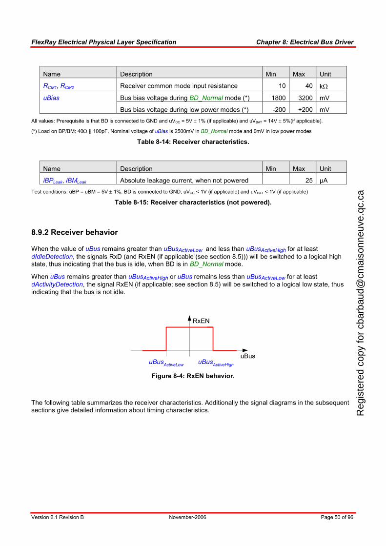
FlexRay Electrical Physical Layer Specification Chapter 8: Electrical Bus Driver
Version 2.1 Revision B November-2006 Page 50 of 96
Name Description Min Max Unit
RCM1, RCM2 Receiver common mode input resistance 10 40 kΩ
Bus bias voltage during BD_Normal mode (*) 1800 3200 mV uBias
Bus bias voltage during low power modes (*) -200 +200 mV
All values: Prerequisite is that BD is connected to GND and uVCC = 5V ± 1% (if applicable) and uVBAT = 14V ± 5%(if applicable).
(*) Load on BP/BM: 40Ω || 100pF. Nominal voltage of uBias is 2500mV in BD_Normal mode and 0mV in low power modes
Table 8-14: Receiver characteristics.
Name Description Min Max Unit
iBPLeak, iBMLeak Absolute leakage current, when not powered 25 µA
Test conditions: uBP = uBM = 5V ± 1%. BD is connected to GND, uVCC < 1V (if applicable) and uVBAT < 1V (if applicable)
Table 8-15: Receiver characteristics (not powered).
8.9.2 Receiver behavior
When the value of uBus remains greater than uBusActiveLow and less than uBusActiveHigh for at least
dIdleDetection, the signals RxD (and RxEN (if applicable (see section 8.5))) will be switched to a logical high state, thus indicating that the bus is idle, when BD is in BD_Normal mode.
When uBus remains greater than uBusActiveHigh or uBus remains less than uBusActiveLow for at least
dActivityDetection, the signal RxEN (if applicable; see section 8.5) will be switched to a logical low state, thus indicating that the bus is not idle.
uBus
RxEN
uBusActiveLow
uBusActiveHigh
Figure 8-4: RxEN behavior.
The following table summarizes the receiver characteristics. Additionally the signal diagrams in the subsequent sections give detailed information about timing characteristics. R
egis
tere
d co
py fo
r cb
arba
ud@
cmai
sonn
euve
.qc.
ca
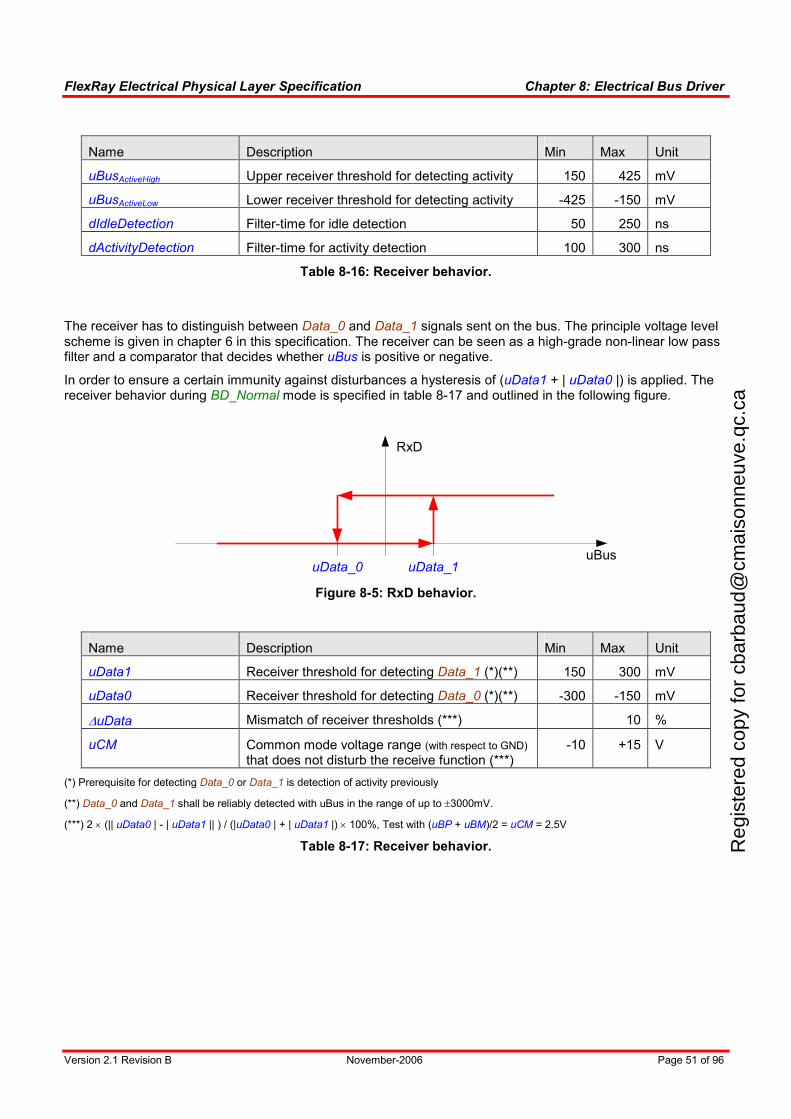
FlexRay Electrical Physical Layer Specification Chapter 8: Electrical Bus Driver
Version 2.1 Revision B November-2006 Page 51 of 96
Name Description Min Max Unit
uBusActiveHigh Upper receiver threshold for detecting activity 150 425 mV
uBusActiveLow Lower receiver threshold for detecting activity -425 -150 mV
dIdleDetection Filter-time for idle detection 50 250 ns
dActivityDetection Filter-time for activity detection 100 300 ns
Table 8-16: Receiver behavior.
The receiver has to distinguish between Data_0 and Data_1 signals sent on the bus. The principle voltage level scheme is given in chapter 6 in this specification. The receiver can be seen as a high-grade non-linear low pass filter and a comparator that decides whether uBus is positive or negative.
In order to ensure a certain immunity against disturbances a hysteresis of (uData1 + | uData0 |) is applied. The receiver behavior during BD_Normal mode is specified in table 8-17 and outlined in the following figure.
uBus
RxD
uData_0 uData_1
Figure 8-5: RxD behavior.
Name Description Min Max Unit
uData1 Receiver threshold for detecting Data_1 (*)(**) 150 300 mV
uData0 Receiver threshold for detecting Data_0 (*)(**) -300 -150 mV
∆uData Mismatch of receiver thresholds (***) 10 %
uCM Common mode voltage range (with respect to GND) that does not disturb the receive function (***)
-10 +15 V
(*) Prerequisite for detecting Data_0 or Data_1 is detection of activity previously
(**) Data_0 and Data_1 shall be reliably detected with uBus in the range of up to ±3000mV.
(***) 2 × (|| uData0 | - | uData1 || ) / (|uData0 | + | uData1 |) × 100%, Test with (uBP + uBM)/2 = uCM = 2.5V
Table 8-17: Receiver behavior.
Reg
iste
red
copy
for
cbar
baud
@cm
aiso
nneu
ve.q
c.ca
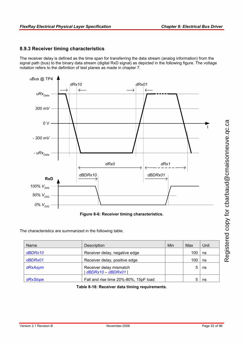
FlexRay Electrical Physical Layer Specification Chapter 8: Electrical Bus Driver
Version 2.1 Revision B November-2006 Page 52 of 96
8.9.3 Receiver timing characteristics
The receiver delay is defined as the time span for transferring the data stream (analog information) from the signal path (bus) to the binary data stream (digital RxD signal) as depicted in the following figure. The voltage notation refers to the definition of test planes as made in chapter 7.
0 V
- uRxData
uRxData
RxDdBDRx10 dBDRx01
uBus @ TP4
t
dRx10 dRx01
- 300 mV
300 mV
100% VDIG
dRx0 dRx1
0% VDIG
50% VDIG
Figure 8-6: Receiver timing characteristics.
The characteristics are summarized in the following table.
Name Description Min Max Unit
dBDRx10 Receiver delay, negative edge 100 ns
dBDRx01 Receiver delay, positive edge 100 ns
dRxAsym Receiver delay mismatch | dBDRx10 – dBDRx01 |
5 ns
dRxSlope Fall and rise time 20%-80%, 15pF load 5 ns
Table 8-18: Receiver data timing requirements.
Reg
iste
red
copy
for
cbar
baud
@cm
aiso
nneu
ve.q
c.ca

FlexRay Electrical Physical Layer Specification Chapter 8: Electrical Bus Driver
Version 2.1 Revision B November-2006 Page 53 of 96
The values in table 8-18 shall be met under the following conditions:
Name Description Min Max Unit
uRxData uBus @ TP4 400 410 mV
dRx10 Transition time Data_1 ⇒ Data_0 21.5 22.5 ns
dRx01 Transition time Data_0 ⇒ Data_1 21.5 22.5 ns
dRx0 Time span Data_0 (*) 80 120 ns
dRx1 Time span Data_1 (*) 80 120 ns
(*) dRx1 + dRx0 = 200ns (± 1ns)
Table 8-19: Receiver input test signal for data recognition.
Reg
iste
red
copy
for
cbar
baud
@cm
aiso
nneu
ve.q
c.ca
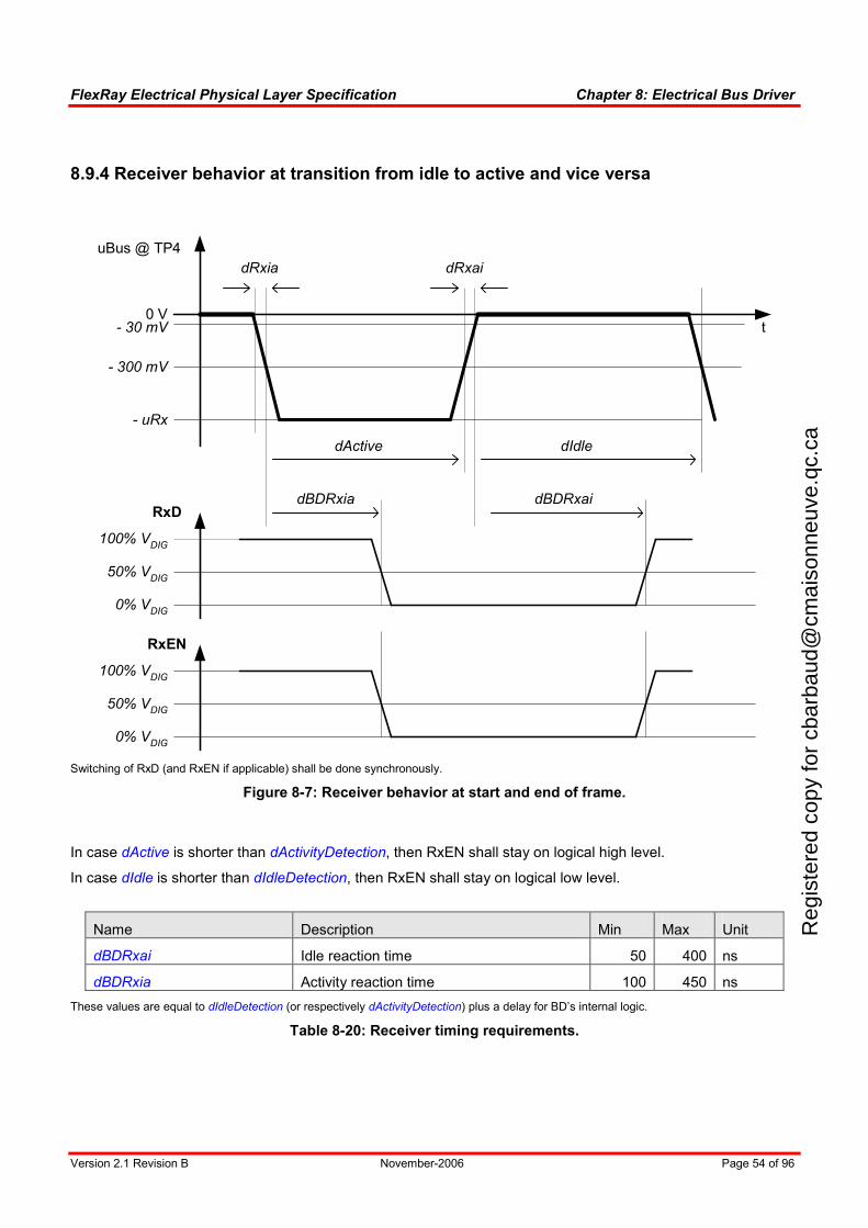
FlexRay Electrical Physical Layer Specification Chapter 8: Electrical Bus Driver
Version 2.1 Revision B November-2006 Page 54 of 96
8.9.4 Receiver behavior at transition from idle to active and vice versa
0 V
- uRx
RxDdBDRxia dBDRxai
uBus @ TP4
t
dRxia dRxai
- 300 mV
dActive
RxEN
dIdle
- 30 mV
100% VDIG
0% VDIG
50% VDIG
100% VDIG
0% VDIG
50% VDIG
Switching of RxD (and RxEN if applicable) shall be done synchronously.
Figure 8-7: Receiver behavior at start and end of frame.
In case dActive is shorter than dActivityDetection, then RxEN shall stay on logical high level.
In case dIdle is shorter than dIdleDetection, then RxEN shall stay on logical low level.
Name Description Min Max Unit
dBDRxai Idle reaction time 50 400 ns
dBDRxia Activity reaction time 100 450 ns
These values are equal to dIdleDetection (or respectively dActivityDetection) plus a delay for BD’s internal logic.
Table 8-20: Receiver timing requirements.
Reg
iste
red
copy
for
cbar
baud
@cm
aiso
nneu
ve.q
c.ca
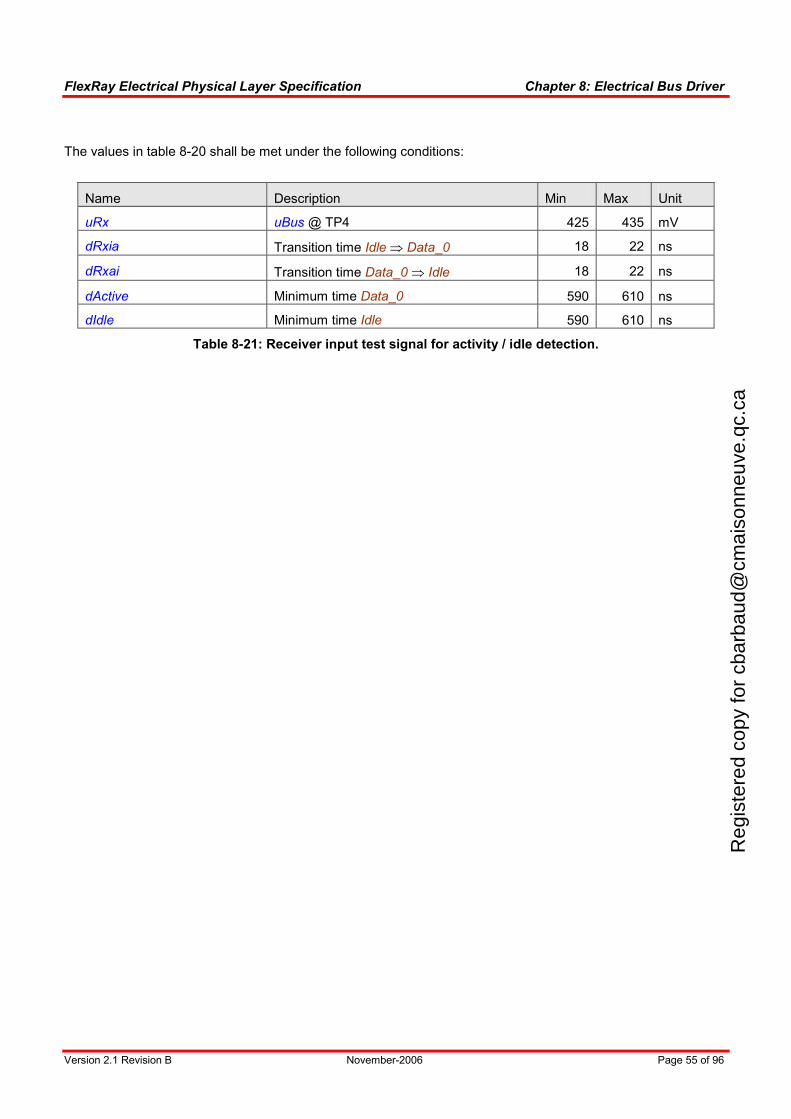
FlexRay Electrical Physical Layer Specification Chapter 8: Electrical Bus Driver
Version 2.1 Revision B November-2006 Page 55 of 96
The values in table 8-20 shall be met under the following conditions:
Name Description Min Max Unit
uRx uBus @ TP4 425 435 mV
dRxia Transition time Idle ⇒ Data_0 18 22 ns
dRxai Transition time Data_0 ⇒ Idle 18 22 ns
dActive Minimum time Data_0 590 610 ns
dIdle Minimum time Idle 590 610 ns
Table 8-21: Receiver input test signal for activity / idle detection.
Reg
iste
red
copy
for
cbar
baud
@cm
aiso
nneu
ve.q
c.ca
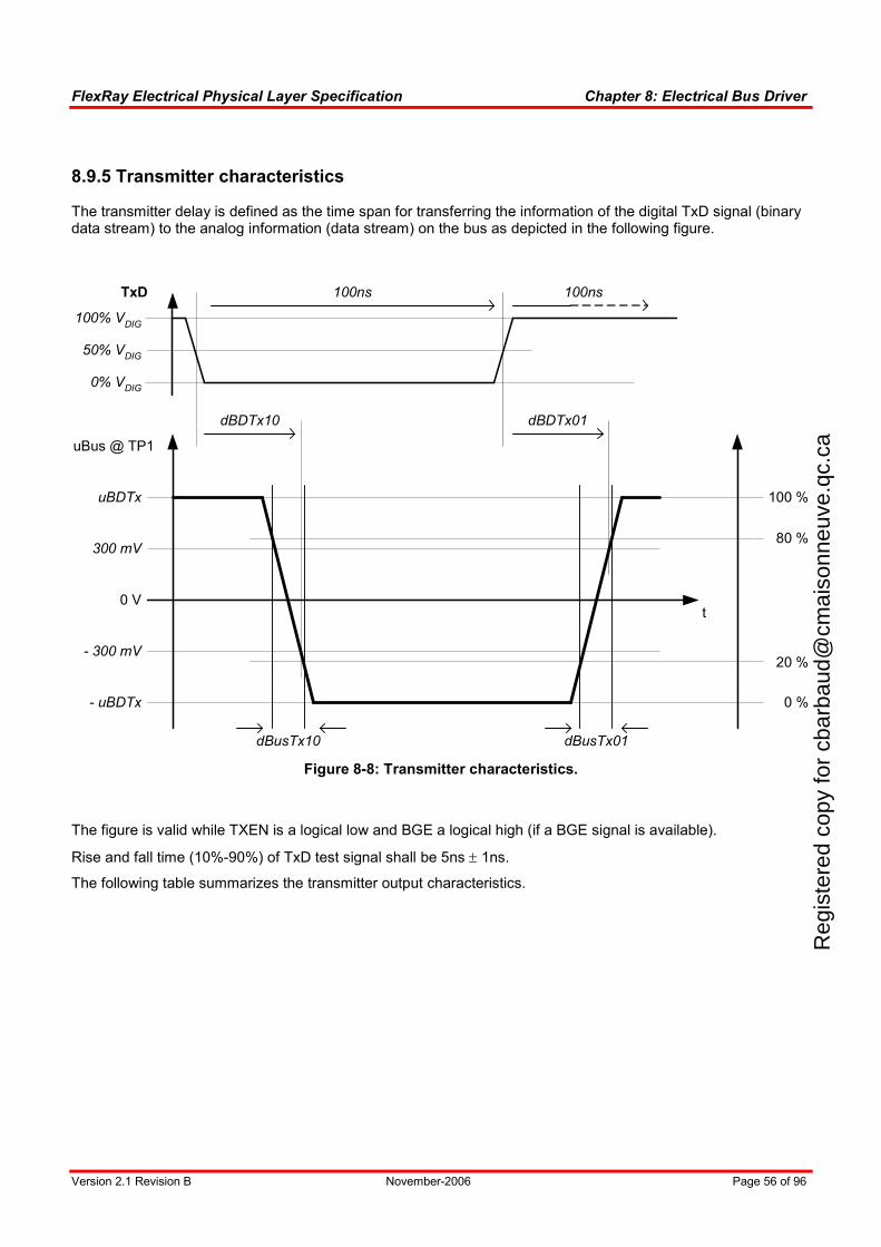
FlexRay Electrical Physical Layer Specification Chapter 8: Electrical Bus Driver
Version 2.1 Revision B November-2006 Page 56 of 96
8.9.5 Transmitter characteristics
The transmitter delay is defined as the time span for transferring the information of the digital TxD signal (binary data stream) to the analog information (data stream) on the bus as depicted in the following figure.
0 V
- uBDTx
uBDTx
TxD
dBDTx10 dBDTx01
uBus @ TP1
t
dBusTx10 dBusTx01
- 300 mV
300 mV
100ns 100ns
100 %
80 %
20 %
0 %
100% VDIG
0% VDIG
50% VDIG
Figure 8-8: Transmitter characteristics.
The figure is valid while TXEN is a logical low and BGE a logical high (if a BGE signal is available).
Rise and fall time (10%-90%) of TxD test signal shall be 5ns ± 1ns.
The following table summarizes the transmitter output characteristics.
Reg
iste
red
copy
for
cbar
baud
@cm
aiso
nneu
ve.q
c.ca
FlexRay Electrical Physical Layer Specification Chapter 8: Electrical Bus Driver
Version 2.1 Revision B November-2006 Page 57 of 96
Name Description Min Max Unit
uBDTxactive Absolute value of uBus, while sending (*) 600 2000 mV
uBDTxidle Absolute value of uBus, while Idle (*) 0 30 mV
dBDTx10 Transmitter delay, negative edge 100 ns
dBDTx01 Transmitter delay, positive edge 100 ns
dTxAsym Transmitter delay mismatch (**) | dBDTx10 - dBDTx01 |
4 ns
dBusTx10 Fall time differential bus voltage (***) (80% → 20%)
3.75 18.75 ns
dBusTx01 Rise time differential bus voltage (***) (20% → 80%)
3.75 18.75 ns
(*) Load on BP/BM: 40Ω || 100pF.
(**) TxD test signal slope (10%-90%) shall be 5ns ± 1ns
(***) Load on BP/BM: 45Ω || 100pF.
Table 8-22: Transmitter characteristics.
Reg
iste
red
copy
for
cbar
baud
@cm
aiso
nneu
ve.q
c.ca
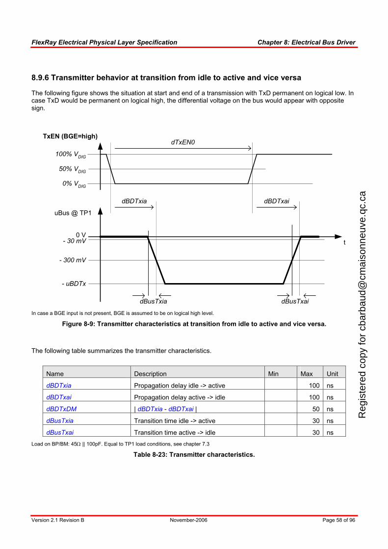
FlexRay Electrical Physical Layer Specification Chapter 8: Electrical Bus Driver
Version 2.1 Revision B November-2006 Page 58 of 96
8.9.6 Transmitter behavior at transition from idle to active and vice versa
The following figure shows the situation at start and end of a transmission with TxD permanent on logical low. In case TxD would be permanent on logical high, the differential voltage on the bus would appear with opposite sign.
0 V
- uBDTx
TxEN (BGE=high)
dBDTxia dBDTxai
uBus @ TP1
t
dBusTxia dBusTxai
- 300 mV
dTxEN0
- 30 mV
100% VDIG
0% VDIG
50% VDIG
In case a BGE input is not present, BGE is assumed to be on logical high level.
Figure 8-9: Transmitter characteristics at transition from idle to active and vice versa.
The following table summarizes the transmitter characteristics.
Name Description Min Max Unit
dBDTxia Propagation delay idle -> active 100 ns
dBDTxai Propagation delay active -> idle 100 ns
dBDTxDM | dBDTxia - dBDTxai | 50 ns
dBusTxia Transition time idle -> active 30 ns
dBusTxai Transition time active -> idle 30 ns
Load on BP/BM: 45Ω || 100pF. Equal to TP1 load conditions, see chapter 7.3
Table 8-23: Transmitter characteristics.
Reg
iste
red
copy
for
cbar
baud
@cm
aiso
nneu
ve.q
c.ca
FlexRay Electrical Physical Layer Specification Chapter 8: Electrical Bus Driver
Version 2.1 Revision B November-2006 Page 59 of 96
Name Description Min Max Unit
dTxEN0 Time span of bus activity 550 650 ns
Table 8-24: Transmitter test signal constraint.
8.9.7 Bus Driver - bus interface behavior, when not powered
In case no supply voltage is available, the transmitter and receiver shall behave like in a low power mode. However, the values for RCM1 and RCM2 may exceed the maximum value as given in table 8-14.
8.9.8 Bus Driver - bus interface behavior under short-circuit conditions
The current flowing from the BD into the bus wires shall be limited in case of short circuits.
Name Description Min Max Unit
iBPBMShortMax, iBMBPShortMax
Absolute maximum output current when BP shorted to BM
100 mA
iBPGNDShortMax, iBMGNDShortMax
Absolute maximum output current when shorted to GND
100 mA
iBP-5VShortMax, iBM-5VShortMax
Absolute maximum output current when shorted to –5V
100 mA
iBPBAT27ShortMax, iBMBAT27ShortMax
Absolute maximum output current when shorted to 27V
100 mA
iBPBAT48ShortMax, iBMBAT48ShortMax
Absolute maximum output current when shorted to 48V (*)
120 mA
iBPBAT60ShortMax, iBMBAT60ShortMax
Absolute maximum output current when shorted to 60V for maximum 400ms (**)(*)
150 mA
(*) these limitations are only valid for devices that are meant to be used in 42V systems
(**) 400ms originated from load dump conditions
Table 8-25: Current limitations.
R
egis
tere
d co
py fo
r cb
arba
ud@
cmai
sonn
euve
.qc.
ca
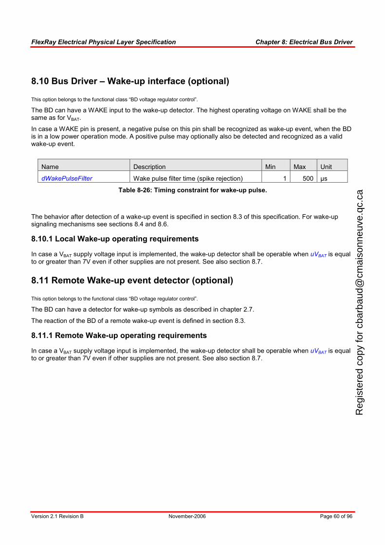
FlexRay Electrical Physical Layer Specification Chapter 8: Electrical Bus Driver
Version 2.1 Revision B November-2006 Page 60 of 96
8.10 Bus Driver – Wake-up interface (optional)
This option belongs to the functional class “BD voltage regulator control”.
The BD can have a WAKE input to the wake-up detector. The highest operating voltage on WAKE shall be the same as for VBAT.
In case a WAKE pin is present, a negative pulse on this pin shall be recognized as wake-up event, when the BD is in a low power operation mode. A positive pulse may optionally also be detected and recognized as a valid wake-up event.
Name Description Min Max Unit
dWakePulseFilter Wake pulse filter time (spike rejection) 1 500 µs
Table 8-26: Timing constraint for wake-up pulse.
The behavior after detection of a wake-up event is specified in section 8.3 of this specification. For wake-up signaling mechanisms see sections 8.4 and 8.6.
8.10.1 Local Wake-up operating requirements
In case a VBAT supply voltage input is implemented, the wake-up detector shall be operable when uVBAT is equal to or greater than 7V even if other supplies are not present. See also section 8.7.
8.11 Remote Wake-up event detector (optional)
This option belongs to the functional class “BD voltage regulator control”.
The BD can have a detector for wake-up symbols as described in chapter 2.7.
The reaction of the BD of a remote wake-up event is defined in section 8.3.
8.11.1 Remote Wake-up operating requirements
In case a VBAT supply voltage input is implemented, the wake-up detector shall be operable when uVBAT is equal to or greater than 7V even if other supplies are not present. See also section 8.7.
Reg
iste
red
copy
for
cbar
baud
@cm
aiso
nneu
ve.q
c.ca
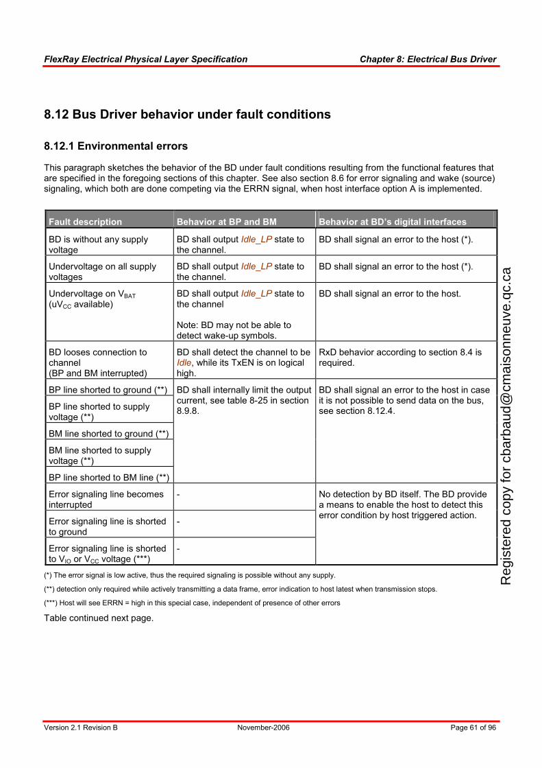
FlexRay Electrical Physical Layer Specification Chapter 8: Electrical Bus Driver
Version 2.1 Revision B November-2006 Page 61 of 96
8.12 Bus Driver behavior under fault conditions
8.12.1 Environmental errors
This paragraph sketches the behavior of the BD under fault conditions resulting from the functional features that are specified in the foregoing sections of this chapter. See also section 8.6 for error signaling and wake (source) signaling, which both are done competing via the ERRN signal, when host interface option A is implemented.
Fault description Behavior at BP and BM Behavior at BD’s digital interfaces
BD is without any supply voltage
BD shall output Idle_LP state to the channel.
BD shall signal an error to the host (*).
Undervoltage on all supply voltages
BD shall output Idle_LP state to the channel.
BD shall signal an error to the host (*).
Undervoltage on VBAT (uVCC available)
BD shall output Idle_LP state to the channel Note: BD may not be able to detect wake-up symbols.
BD shall signal an error to the host.
BD looses connection to channel (BP and BM interrupted)
BD shall detect the channel to be Idle, while its TxEN is on logical high.
RxD behavior according to section 8.4 is required.
BP line shorted to ground (**)
BP line shorted to supply voltage (**)
BM line shorted to ground (**)
BM line shorted to supply voltage (**)
BP line shorted to BM line (**)
BD shall internally limit the output current, see table 8-25 in section 8.9.8.
BD shall signal an error to the host in case it is not possible to send data on the bus, see section 8.12.4.
Error signaling line becomes interrupted
-
Error signaling line is shorted to ground
-
Error signaling line is shorted to VIO or VCC voltage (***)
-
No detection by BD itself. The BD provide a means to enable the host to detect this error condition by host triggered action.
(*) The error signal is low active, thus the required signaling is possible without any supply.
(**) detection only required while actively transmitting a data frame, error indication to host latest when transmission stops.
(***) Host will see ERRN = high in this special case, independent of presence of other errors
Table continued next page.
Reg
iste
red
copy
for
cbar
baud
@cm
aiso
nneu
ve.q
c.ca
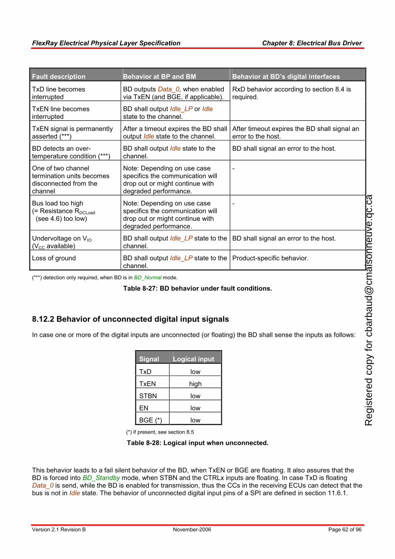
FlexRay Electrical Physical Layer Specification Chapter 8: Electrical Bus Driver
Version 2.1 Revision B November-2006 Page 62 of 96
Fault description Behavior at BP and BM Behavior at BD’s digital interfaces
TxD line becomes interrupted
BD outputs Data_0, when enabled via TxEN (and BGE, if applicable).
TxEN line becomes interrupted
BD shall output Idle_LP or Idle state to the channel.
RxD behavior according to section 8.4 is required.
TxEN signal is permanently asserted (***)
After a timeout expires the BD shall output Idle state to the channel.
After timeout expires the BD shall signal an error to the host.
BD detects an over-temperature condition (***)
BD shall output Idle state to the channel.
BD shall signal an error to the host.
One of two channel termination units becomes disconnected from the channel
Note: Depending on use case specifics the communication will drop out or might continue with degraded performance.
-
Bus load too high (= Resistance RDCLoad (see 4.6) too low)
Note: Depending on use case specifics the communication will drop out or might continue with degraded performance.
-
Undervoltage on VIO (VCC available)
BD shall output Idle_LP state to the channel.
BD shall signal an error to the host.
Loss of ground BD shall output Idle_LP state to the channel.
Product-specific behavior.
(***) detection only required, when BD is in BD_Normal mode.
Table 8-27: BD behavior under fault conditions.
8.12.2 Behavior of unconnected digital input signals
In case one or more of the digital inputs are unconnected (or floating) the BD shall sense the inputs as follows:
Signal Logical input
TxD low
TxEN high
STBN low
EN low
BGE (*) low
(*) if present, see section 8.5
Table 8-28: Logical input when unconnected.
This behavior leads to a fail silent behavior of the BD, when TxEN or BGE are floating. It also assures that the BD is forced into BD_Standby mode, when STBN and the CTRLx inputs are floating. In case TxD is floating Data_0 is send, while the BD is enabled for transmission, thus the CCs in the receiving ECUs can detect that the bus is not in Idle state. The behavior of unconnected digital input pins of a SPI are defined in section 11.6.1.
Reg
iste
red
copy
for
cbar
baud
@cm
aiso
nneu
ve.q
c.ca
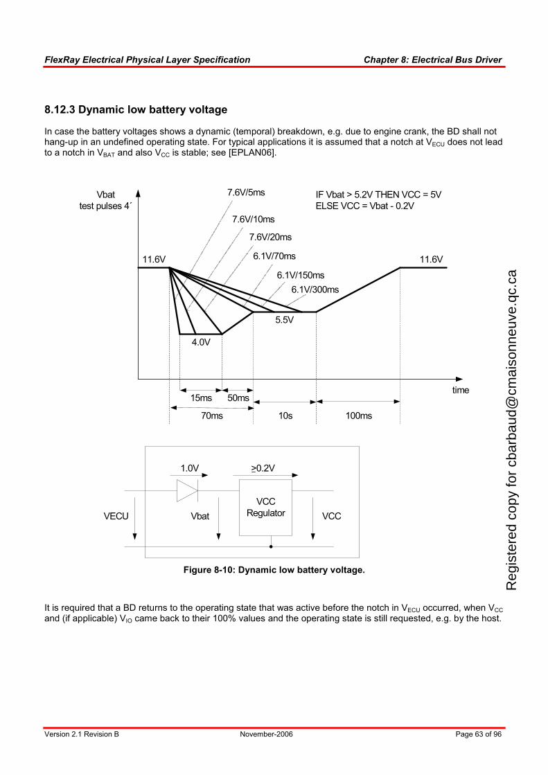
FlexRay Electrical Physical Layer Specification Chapter 8: Electrical Bus Driver
Version 2.1 Revision B November-2006 Page 63 of 96
8.12.3 Dynamic low battery voltage
In case the battery voltages shows a dynamic (temporal) breakdown, e.g. due to engine crank, the BD shall not hang-up in an undefined operating state. For typical applications it is assumed that a notch at VECU does not lead to a notch in VBAT and also VCC is stable; see [EPLAN06].
time
Vbat
test pulses 4´
11.6V
5.5V
7.6V/5ms
11.6V
4.0V
100ms10s70ms
15ms 50ms
7.6V/10ms
7.6V/20ms
6.1V/70ms
6.1V/150ms
6.1V/300ms
IF Vbat > 5.2V THEN VCC = 5V
ELSE VCC = Vbat - 0.2V
VCC
Regulator VCCVbatVECU
1.0V >0.2V
Figure 8-10: Dynamic low battery voltage.
It is required that a BD returns to the operating state that was active before the notch in VECU occurred, when VCC and (if applicable) VIO came back to their 100% values and the operating state is still requested, e.g. by the host.
Reg
iste
red
copy
for
cbar
baud
@cm
aiso
nneu
ve.q
c.ca
FlexRay Electrical Physical Layer Specification Chapter 8: Electrical Bus Driver
Version 2.1 Revision B November-2006 Page 64 of 96
8.12.4 Bus failure detection
The BD shall provide a means to detect bus failures. The host shall be enabled to access bus failure status information via the bus driver - host interface. A single indication “bus failure detected” is sufficient to fulfill this FlexRay requirement. See also table 8-27.
8.12.5 Over-temperature protection
The BD shall provide a means to monitor the junction temperature on the silicon die. If a certain product specific threshold is exceeded, the BD shall disable the transmitter in order to prevent further heating of the chip. Entering a low power mode on over temperature is not acceptable. Receive function shall be maintained as long as possible. The BD shall provide over-temperature information on the bus driver - host interface.
Reg
iste
red
copy
for
cbar
baud
@cm
aiso
nneu
ve.q
c.ca

FlexRay Electrical Physical Layer Specification Chapter 8: Electrical Bus Driver
Version 2.1 Revision B November-2006 Page 65 of 96
8.13 Bus Driver functional classes
Each functional class combines a set of specified options, which have to be coexistent when implemented. These functional classes can be implemented in order to enhance the set of functional features of FlexRay physical layer devices.
8.13.1 Functional class “Bus Driver voltage regulator control”
This class groups the following options, that shall be coexistent, when implemented:
• “VBAT” power supply input; see section 8.7
• Local wake-up detection / WAKE pin; see section 8.10
• Remote wake-up detection; see section 8.11
• “INH1” output signal; see section 8.7.3
• BD_Sleep mode; see section 8.2.
• CTRL2 as second mode control pin (*), in case the host interface is not a SPI.
(*) Instead of 'CTRL2' a product specific name can be used
8.13.2 Functional class “Bus Driver - Bus Guardian interface”
This class comprises the interface as described in section 8.5.
8.13.3 Functional class “Bus Driver internal voltage regulator”
This class comprises the implementation of a “VBAT” power supply input and requires that the BD is fully operational without a VCC supply input. If this functional class is implemented the functional class 'Bus Driver logic level adaptation' shall be implemented also.
8.13.4 Functional class “Bus Driver logic level adaptation”
This class comprises the implementation of a bus driver level shift interface and requires that the thresholds of all digital inputs are controlled by this voltage as well as all digital outputs are related to this voltage level. See also section 8.8 and chapter 11.
R
egis
tere
d co
py fo
r cb
arba
ud@
cmai
sonn
euve
.qc.
ca
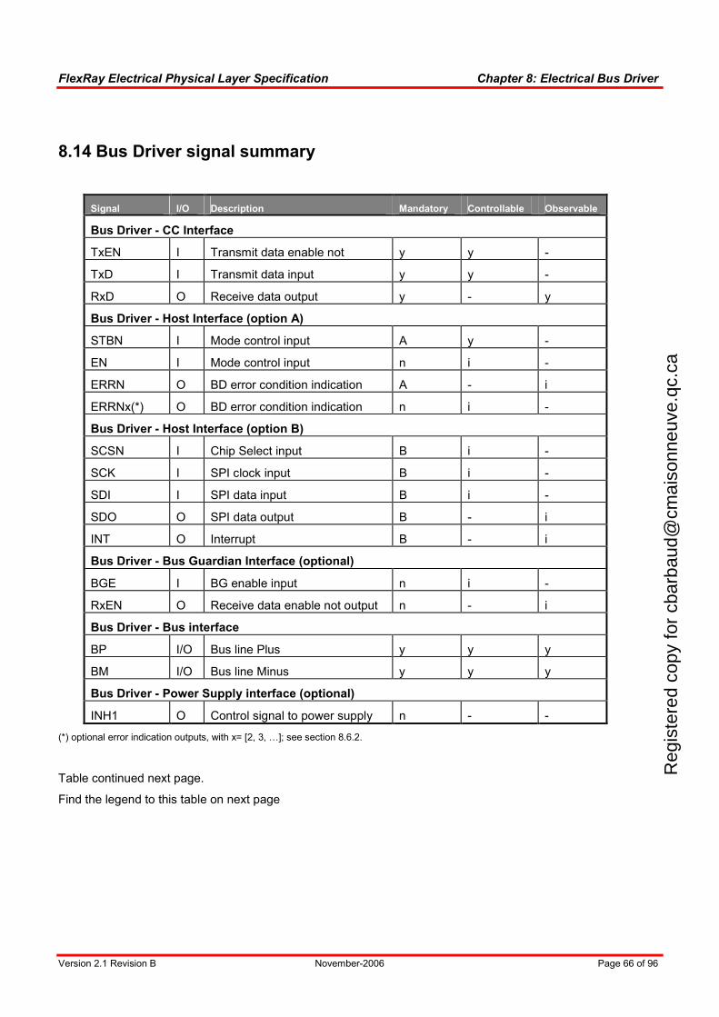
FlexRay Electrical Physical Layer Specification Chapter 8: Electrical Bus Driver
Version 2.1 Revision B November-2006 Page 66 of 96
8.14 Bus Driver signal summary
Signal I/O Description Mandatory Controllable Observable
Bus Driver - CC Interface
TxEN I Transmit data enable not y y -
TxD I Transmit data input y y -
RxD O Receive data output y - y
Bus Driver - Host Interface (option A)
STBN I Mode control input A y -
EN I Mode control input n i -
ERRN O BD error condition indication A - i
ERRNx(*) O BD error condition indication n i -
Bus Driver - Host Interface (option B)
SCSN I Chip Select input B i -
SCK I SPI clock input B i -
SDI I SPI data input B i -
SDO O SPI data output B - i
INT O Interrupt B - i
Bus Driver - Bus Guardian Interface (optional)
BGE I BG enable input n i -
RxEN O Receive data enable not output n - i
Bus Driver - Bus interface
BP I/O Bus line Plus y y y
BM I/O Bus line Minus y y y
Bus Driver - Power Supply interface (optional)
INH1 O Control signal to power supply n - -
(*) optional error indication outputs, with x= [2, 3, …]; see section 8.6.2.
Table continued next page.
Find the legend to this table on next page
Reg
iste
red
copy
for
cbar
baud
@cm
aiso
nneu
ve.q
c.ca
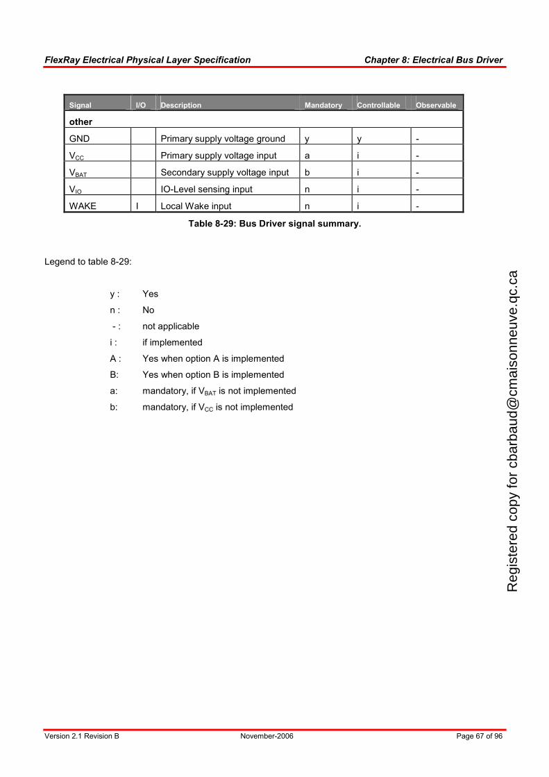
FlexRay Electrical Physical Layer Specification Chapter 8: Electrical Bus Driver
Version 2.1 Revision B November-2006 Page 67 of 96
Signal I/O Description Mandatory Controllable Observable
other
GND Primary supply voltage ground y y -
VCC Primary supply voltage input a i -
VBAT Secondary supply voltage input b i -
VIO IO-Level sensing input n i -
WAKE I Local Wake input n i -
Table 8-29: Bus Driver signal summary.
Legend to table 8-29:
y : Yes
n : No
- : not applicable
i : if implemented
A : Yes when option A is implemented
B: Yes when option B is implemented
a: mandatory, if VBAT is not implemented
b: mandatory, if VCC is not implemented
Reg
iste
red
copy
for
cbar
baud
@cm
aiso
nneu
ve.q
c.ca
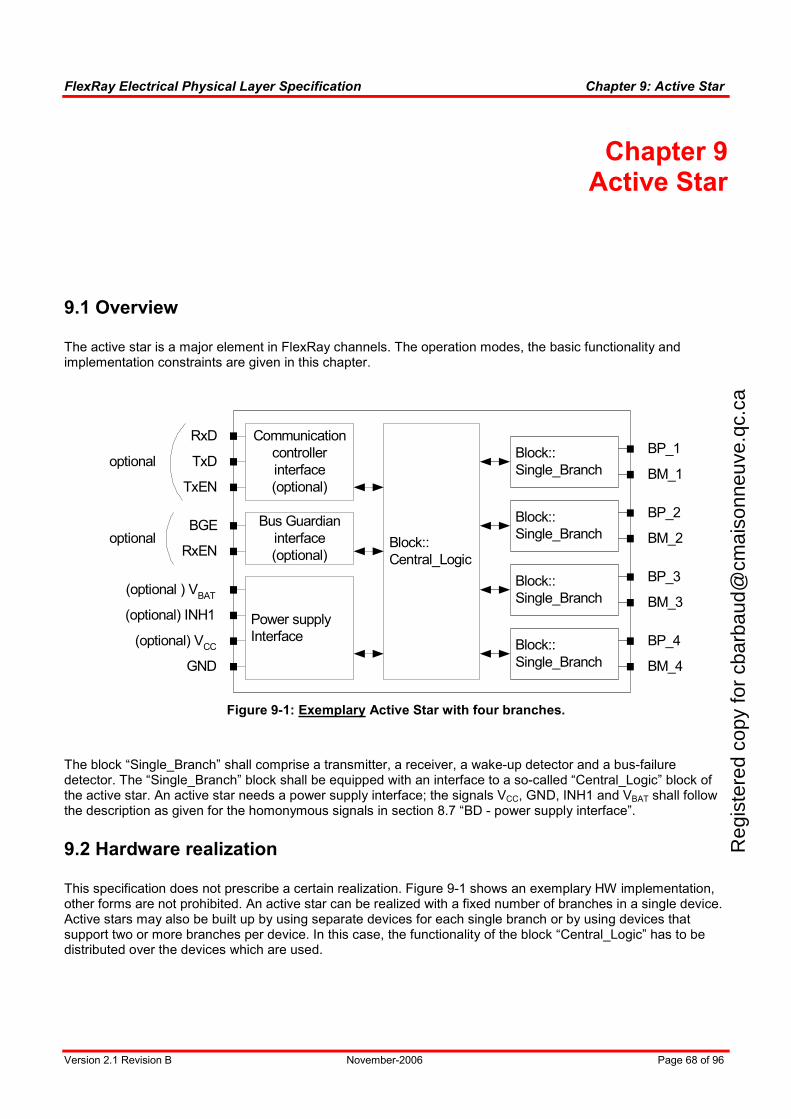
FlexRay Electrical Physical Layer Specification Chapter 9: Active Star
Version 2.1 Revision B November-2006 Page 68 of 96
Chapter 9 Active Star
9.1 Overview
The active star is a major element in FlexRay channels. The operation modes, the basic functionality and implementation constraints are given in this chapter.
Block::
Single_BranchBlock::
Central_Logic
BP_2
BM_2
(optional) INH1
(optional) VCC
(optional ) VBAT
GND
Block::
Single_Branch
BP_1
BM_1
Block::
Single_Branch
BP_3
BM_3
Block::
Single_Branch
BP_4
BM_4
Power supply
Interface
Communication
controller
interface
(optional)
Bus Guardian
interface
(optional)
BGE
TxEN
TxD
RxD
RxEN
optional
optional
Figure 9-1: Exemplary Active Star with four branches.
The block “Single_Branch” shall comprise a transmitter, a receiver, a wake-up detector and a bus-failure detector. The “Single_Branch” block shall be equipped with an interface to a so-called “Central_Logic” block of the active star. An active star needs a power supply interface; the signals VCC, GND, INH1 and VBAT shall follow the description as given for the homonymous signals in section 8.7 “BD - power supply interface”.
9.2 Hardware realization
This specification does not prescribe a certain realization. Figure 9-1 shows an exemplary HW implementation, other forms are not prohibited. An active star can be realized with a fixed number of branches in a single device. Active stars may also be built up by using separate devices for each single branch or by using devices that support two or more branches per device. In this case, the functionality of the block “Central_Logic” has to be distributed over the devices which are used.
Reg
iste
red
copy
for
cbar
baud
@cm
aiso
nneu
ve.q
c.ca
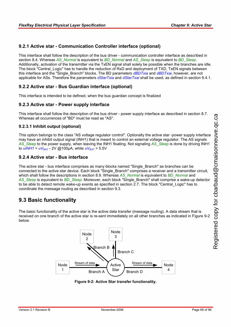
FlexRay Electrical Physical Layer Specification Chapter 9: Active Star
Version 2.1 Revision B November-2006 Page 69 of 96
9.2.1 Active star - Communication Controller interface (optional)
This interface shall follow the description of the bus driver - communication controller interface as described in section 8.4. Whereas AS_Normal is equivalent to BD_Normal and AS_Sleep is equivalent to BD_Sleep. Additionally, activation of the transmitter via the TxEN signal shall solely be possible when the branches are idle. The block "Central_Logic" has to handle the reduction of RxD and deployment of TXD, TxEN signals between this interface and the "Single_Branch" blocks. The BD parameters dBDTxia and dBDTxai, however, are not applicable for ASs. Therefore the parameters dStarTxia and dStarTxai shall be used, as defined in section 9.4.1.
9.2.2 Active star - Bus Guardian interface (optional)
This interface is intended to be defined, when the bus guardian concept is finalized
9.2.3 Active star - Power supply interface
This interface shall follow the description of the bus driver - power supply interface as described in section 8.7. Whereas all occurrences of "BD" must be read as "AS".
9.2.3.1 Inhibit output (optional)
This option belongs to the class "AS voltage regulator control". Optionally the active star -power supply interface may have an inhibit output signal (INH1) that is meant to control an external voltage regulator. The AS signals AS_Sleep to the power supply, when leaving the INH1 floating. Not signaling AS_Sleep is done by driving INH1 to uINH1 > uVBAT - 2V @100µA, while uVBAT > 5.5V
9.2.4 Active star - Bus interface
The active star - bus interface comprises as many blocks named "Single_Branch" as branches can be connected to the active star device. Each block "Single_Branch" comprises a receiver and a transmitter circuit, which shall follow the descriptions in section 8.9. Whereas AS_Normal is equivalent to BD_Normal and AS_Sleep is equivalent to BD_Sleep. Moreover, each block "Single_Branch" shall comprise a wake-up detector to be able to detect remote wake-up events as specified in section 2.7. The block "Central_Logic" has to coordinate the message routing as described in section 9.3.
9.3 Basic functionality
The basic functionality of the active star is the active data transfer (message routing). A data stream that is received on one branch of the active star is re-sent immediately on all other branches as indicated in Figure 9-2 below.
Branch A
Stream of data
Branch BBranch C
Branch D
Stream of dataActive
Star
Node
1
Node
2
Node
4
Node
3
Figure 9-2: Active Star transfer functionality.
Reg
iste
red
copy
for
cbar
baud
@cm
aiso
nneu
ve.q
c.ca
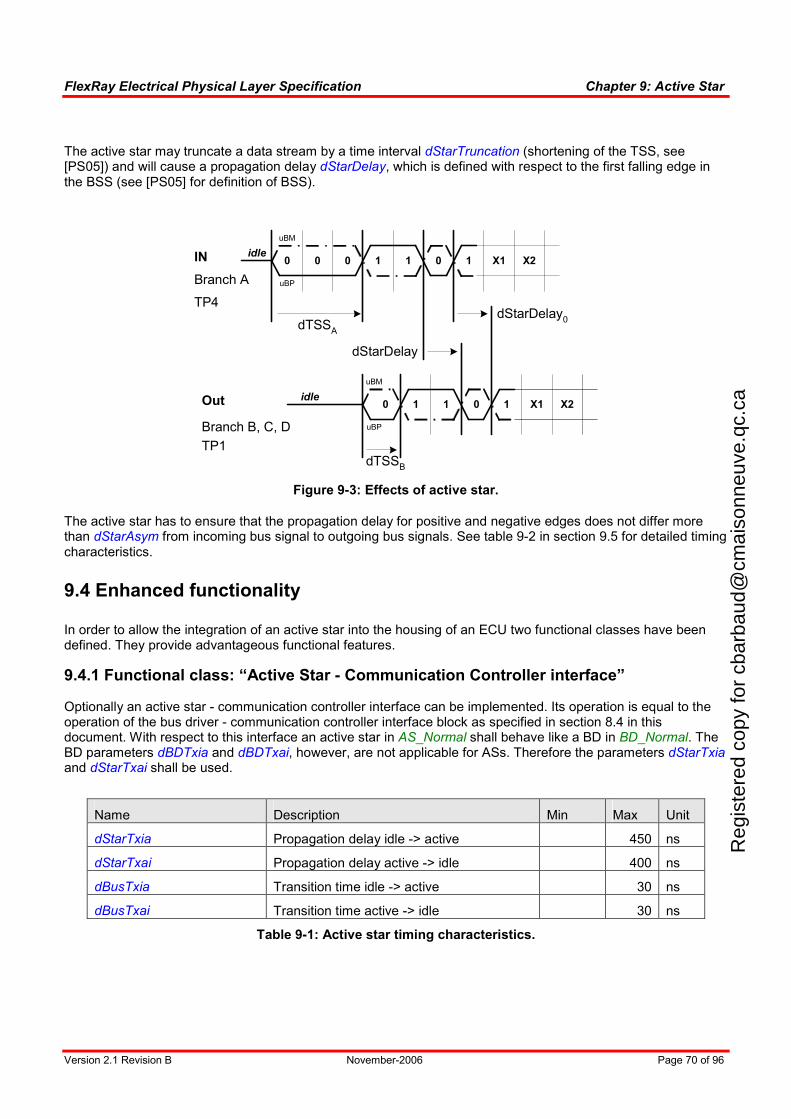
FlexRay Electrical Physical Layer Specification Chapter 9: Active Star
Version 2.1 Revision B November-2006 Page 70 of 96
The active star may truncate a data stream by a time interval dStarTruncation (shortening of the TSS, see [PS05]) and will cause a propagation delay dStarDelay, which is defined with respect to the first falling edge in the BSS (see [PS05] for definition of BSS).
1 0 X1 X20 00
dStarDelay
IN
Out
idle
Branch A
Branch B, C, D
idle
uBP
uBM
uBP
uBM
1 1
1 0 X1 X20 1 1
dStarDelay0
dTSSA
dTSSB
TP4
TP1
Figure 9-3: Effects of active star.
The active star has to ensure that the propagation delay for positive and negative edges does not differ more than dStarAsym from incoming bus signal to outgoing bus signals. See table 9-2 in section 9.5 for detailed timing characteristics.
9.4 Enhanced functionality
In order to allow the integration of an active star into the housing of an ECU two functional classes have been defined. They provide advantageous functional features.
9.4.1 Functional class: “Active Star - Communication Controller interface”
Optionally an active star - communication controller interface can be implemented. Its operation is equal to the operation of the bus driver - communication controller interface block as specified in section 8.4 in this document. With respect to this interface an active star in AS_Normal shall behave like a BD in BD_Normal. The BD parameters dBDTxia and dBDTxai, however, are not applicable for ASs. Therefore the parameters dStarTxia and dStarTxai shall be used.
Name Description Min Max Unit
dStarTxia Propagation delay idle -> active 450 ns
dStarTxai Propagation delay active -> idle 400 ns
dBusTxia Transition time idle -> active 30 ns
dBusTxai Transition time active -> idle 30 ns
Table 9-1: Active star timing characteristics.
Reg
iste
red
copy
for
cbar
baud
@cm
aiso
nneu
ve.q
c.ca
FlexRay Electrical Physical Layer Specification Chapter 9: Active Star
Version 2.1 Revision B November-2006 Page 71 of 96
9.4.2 Functional class: “Active Star - Bus Guardian interface”
In case an active star - communication controller interface is present, an active star - bus guardian interface can be implemented optionally. Its operation is equal to the operation of the bus driver - bus guardian interface as specified in section 8.5 in this document.
9.4.3 Functional class "Active Star - Voltage regulator control"
This class groups the following options:
- VBAT input, see section 9.2.3
- INH1 output, see section 9.2.3.1
9.4.4 Functional class "Active Star - Internal voltage regulator"
This class comprises the implementation of a VBAT power supply input and requires that the AS is fully operational without a VCC supply.
9.5 Active Star timing characteristics
Name Description Min Max Unit
dStarDelay Propagation delay negative edge 250 ns
dStarDelay0 Propagation delay positive edge 250 ns
dStarAsym Asymmetric propagation delay (*) 8 ns
dStarTruncation Truncation (**) 450 ns
(*) dStarAsym = | dStarDelay - dStarDelay0 | (**) dStarTruncation = | dTSSA - dTSSB |
Table 9-2: Active star timing characteristics.
Implementations that do not meet the specified propagation delay maximum are allowed, when digital signal processing is done. The maximum propagation delay for the entire communication channel as specified in section 2.2 must be met.
Non-monolithic implementations of active stars, i.e. active stars that are built up with more than one semiconductor device, are allowed to exceed the limit of dStarAsym by 2ns. In other words: the total maximum asymmetric propagation delay for non-monolithic active stars has to be less than or equal to 10ns.
Reg
iste
red
copy
for
cbar
baud
@cm
aiso
nneu
ve.q
c.ca
FlexRay Electrical Physical Layer Specification Chapter 9: Active Star
Version 2.1 Revision B November-2006 Page 72 of 96
9.6 Active Star operation modes
The AS shall support at least two overall operation modes, which are AS_Sleep and AS_Normal. Furthermore, each branch has its operating states, as described in the following section.
9.6.1 AS_Sleep
The AS_Sleep mode is a so-called low power mode.
The AS is not able to send or receive data from the bus, but AS´s wakeup monitoring functions are active.
The power consumption is significantly reduced compared to AS_Normal.
Sleep is signaled on the INH1 output, in case this signal is implemented.
The bus wires are terminated to GND via the receiver common mode input resistance.
When one of the branches signals the reception of a wake-up event the AS enters AS_Normal.
9.6.2 AS_Normal
The AS is able to send and receive data on the bus and perform the transfer function as described in the previous section of this specification.
Not_Sleep is signaled on the INH1 output, in case this signal is implemented
When all branches are in Branch_Idle or Branch_FailSilent for longer than dStarGoToSleep the AS enters AS_Sleep.
Name Description Min Max Unit
dStarGoToSleep Go-to-Sleep timeout 640 64000 ms
Table 9-3: Active star go-to-sleep timeout.
The minimum of this parameter was chosen to fulfill the following equation:
dStarGoToSleep ≥ 40 × cdCycleMax.
9.6.3 AS_Standby
In AS_Standby Not_Sleep is signaled on the INH output. The AS waits for necessary voltages (e.g. VCC, VIO or internal generated voltages (depends on implementation) to leave the undervoltage range.
Reg
iste
red
copy
for
cbar
baud
@cm
aiso
nneu
ve.q
c.ca
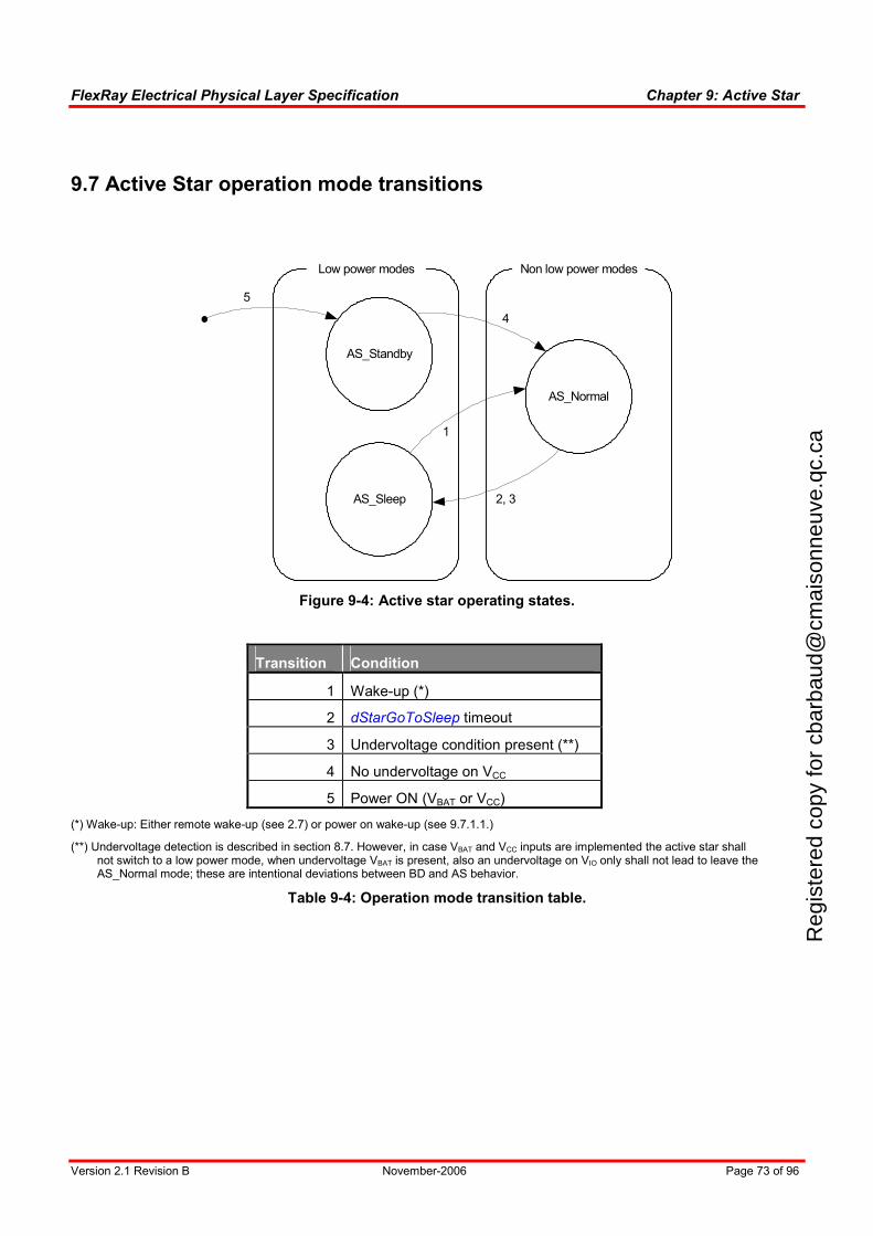
FlexRay Electrical Physical Layer Specification Chapter 9: Active Star
Version 2.1 Revision B November-2006 Page 73 of 96
9.7 Active Star operation mode transitions
AS_Normal
AS_Sleep
Low power modes Non low power modes
2, 3
1
AS_Standby
4
5
Figure 9-4: Active star operating states.
Transition Condition
1 Wake-up (*)
2 dStarGoToSleep timeout
3 Undervoltage condition present (**)
4 No undervoltage on VCC
5 Power ON (VBAT or VCC)
(*) Wake-up: Either remote wake-up (see 2.7) or power on wake-up (see 9.7.1.1.)
(**) Undervoltage detection is described in section 8.7. However, in case VBAT and VCC inputs are implemented the active star shall not switch to a low power mode, when undervoltage VBAT is present, also an undervoltage on VIO only shall not lead to leave the AS_Normal mode; these are intentional deviations between BD and AS behavior.
Table 9-4: Operation mode transition table.
Reg
iste
red
copy
for
cbar
baud
@cm
aiso
nneu
ve.q
c.ca
FlexRay Electrical Physical Layer Specification Chapter 9: Active Star
Version 2.1 Revision B November-2006 Page 74 of 96
9.7.1 Active Star behavior after wake-up
When a remote wake-up event is detected the active star enters AS_Normal as specified above. Implementations of ASs shall guarantee that AS_Normal is entered latest dStarWakeUpReaction after detection of a valid wake-up event. This is to ensure acceptable start up times for FlexRay systems that make use of cascaded ASs. Recall that the FlexRay protocol has a limited capability to send wake-up symbols, therefore it is mandatory that an active star is able to forward at least 30 wake-up symbols while in AS_Sleep, or the active star enters AS_Normal before 33 wake-up symbols have been received; i.e. an active star that receives 63 wake-up symbols has to forward at least 33 of them, an active star that receives 33 wake-up symbols has to forward at least 3 of them.
The corresponding protocol parameters (e.g. pWakeupPattern) have to be taken into account.
Name Description Min Max Unit
dStarWakeUpReaction Active star wake up reaction time 100 ms
Table 9-5: Active star wake-up reaction time.
9.7.1.1 Power on wake-up
The AS shall recognize the event of becoming sufficiently supplied by VBAT as valid wake-up event.
9.8 Operating states of branches
Each branch needs to support the following operating states.
Further product specific operation states are not prohibited.
9.8.1 Branch_Idle
When Idle is detected on the branch and the data interface to the Central_Logic, then the branch enters its Branch_Idle state. The activity detection of this branch is active, the transmitter is disabled. When activity is detected either on the branch or on the data interface to the Central_Logic, the branch enters its Branch_Active state.
9.8.2 Branch_Active
When Branch_Active is entered upon detection of activity on a branch, this branch receives a data stream and passes a binary data stream to the Central_Logic.
When Branch_Active is entered upon a command from the Central_Logic, this branch transmits the binary data stream from the Central_Logic data interface to the branch.
A timer for each branch is started with entering Branch_Active. Upon expiration of such timer after dBranchActive the affected branch is excluded from communication. (I.e. prevention of babbling idiots in absence of BGs.) This branch enters Branch_FailSilent.
9.8.3 Branch_FailSilent
A branch in this state does not pass the received data stream from the branch via the data interface to the Central_Logic; the branch signals Idle to the Central_Logic. It does also not re-enter Branch_Active upon the request of the Central_Logic, while in this state. Idle is signaled on the branch.
Reg
iste
red
copy
for
cbar
baud
@cm
aiso
nneu
ve.q
c.ca
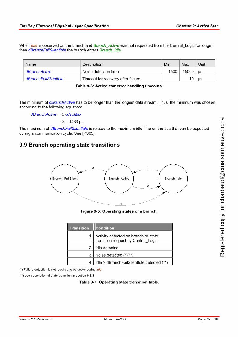
FlexRay Electrical Physical Layer Specification Chapter 9: Active Star
Version 2.1 Revision B November-2006 Page 75 of 96
When Idle is observed on the branch and Branch_Active was not requested from the Central_Logic for longer than dBranchFailSilentIdle the branch enters Branch_Idle.
Name Description Min Max Unit
dBranchActive Noise detection time 1500 15000 µs
dBranchFailSilentIdle Timeout for recovery after failure 10 µs
Table 9-6: Active star error handling timeouts.
The minimum of dBranchActive has to be longer than the longest data stream. Thus, the minimum was chosen according to the following equation:
dBranchActive ≥ cdTxMax
≥ 1433 µs
The maximum of dBranchFailSilentIdle is related to the maximum idle time on the bus that can be expected during a communication cycle. See [PS05].
9.9 Branch operating state transitions
Branch_FailSilent Branch_Active Branch_Idle
1
2
4
3
Figure 9-5: Operating states of a branch.
Transition Condition
1 Activity detected on branch or state transition request by Central_Logic
2 Idle detected
3 Noise detected (*)(**)
4 Idle > dBranchFailSilentIdle detected (**)
(*) Failure detection is not required to be active during idle.
(**) see description of state transition in section 9.8.3
Table 9-7: Operating state transition table.
Reg
iste
red
copy
for
cbar
baud
@cm
aiso
nneu
ve.q
c.ca
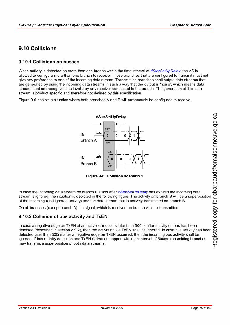
FlexRay Electrical Physical Layer Specification Chapter 9: Active Star
Version 2.1 Revision B November-2006 Page 76 of 96
9.10 Collisions
9.10.1 Collisions on busses
When activity is detected on more than one branch within the time interval of dStarSetUpDelay, the AS is allowed to configure more than one branch to receive. Those branches that are configured to transmit must not give any preference to one of the incoming data stream. Transmitting branches shall output data streams that are generated by using the incoming data streams in such a way that the output is ‘noise’, which means data streams that are recognized as invalid by any receiver connected to the branch. The generation of this data stream is product specific and therefore not defined by this specification.
Figure 9-6 depicts a situation where both branches A and B will erroneously be configured to receive.
IN
Branch A
dStarSetUpDelay
IN
Branch B
10 00idle
uBP
uBM
10 00idle
uBP
uBM
Figure 9-6: Collision scenario 1.
In case the incoming data stream on branch B starts after dStarSetUpDelay has expired the incoming data stream is ignored, the situation is depicted in the following figure. The activity on branch B will be a superposition of the incoming (and ignored activity) and the data stream that is actively transmitted on branch B.
On all branches (except branch A) the signal, which is received on branch A, is re-transmitted.
9.10.2 Collision of bus activity and TxEN
In case a negative edge on TxEN at an active star occurs later than 500ns after activity on bus has been detected (described in section 8.9.2), then the activation via TxEN shall be ignored. In case bus activity has been detected later than 500ns after a negative edge on TxEN occurred, then the incoming bus activity shall be ignored. If bus activity detection and TxEN activation happen within an interval of 500ns transmitting branches may transmit a superposition of both data streams.
Reg
iste
red
copy
for
cbar
baud
@cm
aiso
nneu
ve.q
c.ca
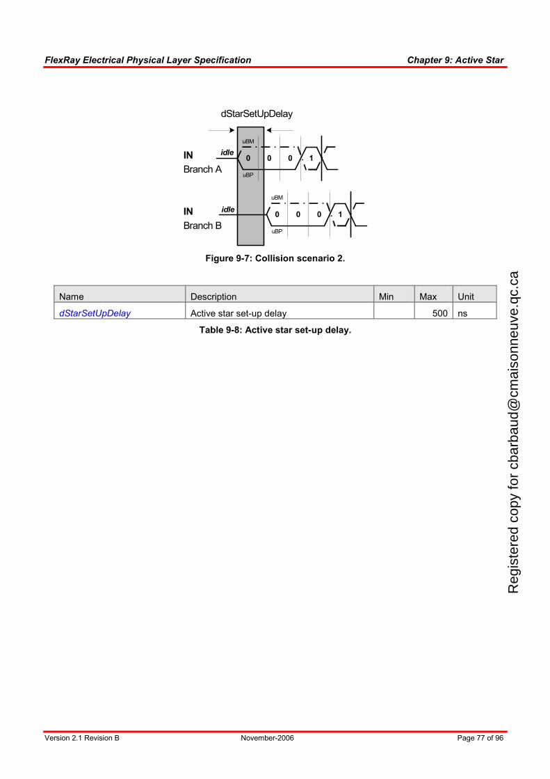
FlexRay Electrical Physical Layer Specification Chapter 9: Active Star
Version 2.1 Revision B November-2006 Page 77 of 96
IN
Branch A
dStarSetUpDelay
IN
Branch B
10 00idle
uBP
uBM
10 00idle
uBP
uBM
Figure 9-7: Collision scenario 2.
Name Description Min Max Unit
dStarSetUpDelay Active star set-up delay 500 ns
Table 9-8: Active star set-up delay.
Reg
iste
red
copy
for
cbar
baud
@cm
aiso
nneu
ve.q
c.ca
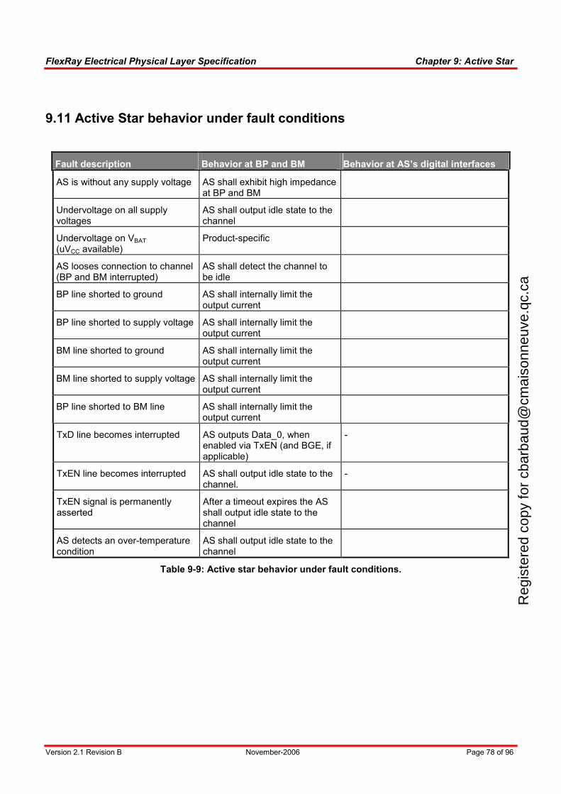
FlexRay Electrical Physical Layer Specification Chapter 9: Active Star
Version 2.1 Revision B November-2006 Page 78 of 96
9.11 Active Star behavior under fault conditions
Fault description Behavior at BP and BM Behavior at AS’s digital interfaces
AS is without any supply voltage AS shall exhibit high impedance at BP and BM
Undervoltage on all supply voltages
AS shall output idle state to the channel
Undervoltage on VBAT (uVCC available)
Product-specific
AS looses connection to channel (BP and BM interrupted)
AS shall detect the channel to be idle
BP line shorted to ground AS shall internally limit the output current
BP line shorted to supply voltage AS shall internally limit the output current
BM line shorted to ground AS shall internally limit the output current
BM line shorted to supply voltage AS shall internally limit the output current
BP line shorted to BM line AS shall internally limit the output current
TxD line becomes interrupted AS outputs Data_0, when enabled via TxEN (and BGE, if applicable)
-
TxEN line becomes interrupted AS shall output idle state to the channel.
-
TxEN signal is permanently asserted
After a timeout expires the AS shall output idle state to the channel
AS detects an over-temperature condition
AS shall output idle state to the channel
Table 9-9: Active star behavior under fault conditions.
Reg
iste
red
copy
for
cbar
baud
@cm
aiso
nneu
ve.q
c.ca
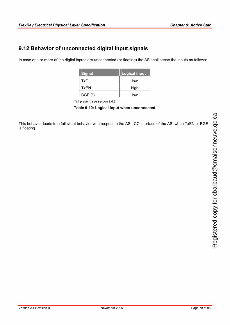
FlexRay Electrical Physical Layer Specification Chapter 9: Active Star
Version 2.1 Revision B November-2006 Page 79 of 96
9.12 Behavior of unconnected digital input signals
In case one or more of the digital inputs are unconnected (or floating) the AS shall sense the inputs as follows:
Signal Logical input
TxD low
TxEN high
BGE (*) low
(*) if present, see section 9.4.2
Table 9-10: Logical input when unconnected.
This behavior leads to a fail silent behavior with respect to the AS - CC interface of the AS, when TxEN or BGE is floating.
Reg
iste
red
copy
for
cbar
baud
@cm
aiso
nneu
ve.q
c.ca
FlexRay Electrical Physical Layer Specification Chapter 10: Bus Guardian
Version 2.1 Revision B November-2006 Page 80 of 96
Chapter 10 Bus Guardian
This chapter needs to be reworked, according to most recent BG concepts.
Reg
iste
red
copy
for
cbar
baud
@cm
aiso
nneu
ve.q
c.ca
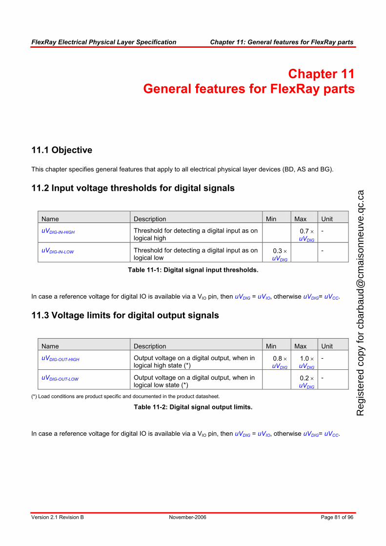
FlexRay Electrical Physical Layer Specification Chapter 11: General features for FlexRay parts
Version 2.1 Revision B November-2006 Page 81 of 96
Chapter 11 General features for FlexRay parts
11.1 Objective
This chapter specifies general features that apply to all electrical physical layer devices (BD, AS and BG).
11.2 Input voltage thresholds for digital signals
Name Description Min Max Unit
uVDIG-IN-HIGH Threshold for detecting a digital input as on logical high
0.7 × uVDIG
-
uVDIG-IN-LOW Threshold for detecting a digital input as on logical low
0.3 × uVDIG
-
Table 11-1: Digital signal input thresholds.
In case a reference voltage for digital IO is available via a VIO pin, then uVDIG = uVIO, otherwise uVDIG= uVCC.
11.3 Voltage limits for digital output signals
Name Description Min Max Unit
uVDIG-OUT-HIGH Output voltage on a digital output, when in logical high state (*)
0.8 × uVDIG
1.0 × uVDIG
-
uVDIG-OUT-LOW Output voltage on a digital output, when in logical low state (*)
0.2 × uVDIG
-
(*) Load conditions are product specific and documented in the product datasheet.
Table 11-2: Digital signal output limits.
In case a reference voltage for digital IO is available via a VIO pin, then uVDIG = uVIO, otherwise uVDIG= uVCC.
Reg
iste
red
copy
for
cbar
baud
@cm
aiso
nneu
ve.q
c.ca
FlexRay Electrical Physical Layer Specification Chapter 11: General features for FlexRay parts
Version 2.1 Revision B November-2006 Page 82 of 96
11.4 ESD protection on chip level
All pins of FlexRay physical layer parts shall be protected against damage by electrostatic discharge (ESD) according to the Human-Body-Model JEDEC JESD22/A114, as referenced by AEC-Q100.
This Human-Body-Model foresees the contact discharge of a 100pF capacitor to the pin under test with an
additional series resistance of 1500Ω.
Those pins of FlexRay parts that are intended to be connected to terminals outside the ECU shall withstand a discharge of uESDExt relative to device's ground pin. All others shall withstand a discharge of uESDInt.
Name Description Min Max Unit
uESDExt ESD protection on pins that lead to ECU external terminals (*)
4 kV
uESDInt ESD on all other pins 2 kV
(*) Typically: BM, BP, WAKE and VBAT.
Table 11-3: ESD protection (HBM).
11.5 ESD protection on ECU level
ESD protection at the ECU level is under the responsibility of the equipment maker and not part of this specification. Find application hints in [EPLAN06] for enhanced ESD protection.
11.6 Operating temperature
All FlexRay physical layer devices shall support operation under automotive environmental temperatures.
Name Description Min Max Unit
T Ambient temperature - 40 + 125 °C
Table 11-4: Operating temperature range.
Reg
iste
red
copy
for
cbar
baud
@cm
aiso
nneu
ve.q
c.ca
FlexRay Electrical Physical Layer Specification Chapter 11: General features for FlexRay parts
Version 2.1 Revision B November-2006 Page 83 of 96
11.7 Serial peripheral interface (SPI)
Any bit sampling is performed with the falling clock edge and the data is shifted with the rising clock edge.
The transfer speed shall at least cover the range from 10kBit/s to 1MBit/s.
01 02 03
X MSB
sampled
14 13 12
03
X MSB 14 13 12
15 16
01 LSB X
01 LSB
SCSN
SDI
SDOfloat
SCK
Figure 11-1: SPI register access.
Within one SCSN cycle (SCSN on logical low), 16 clock periods (SCK) are expected. Any deviation in the number of clock periods is recognized as an error and the access is ignored.
11.7.1 Behavior of unconnected digital input pins
In case one or more of the digital inputs are unconnected (or floating) the SPI shall sense the inputs as follows:
Signal Logical input
SCSN high
SCK high
SDI low
Table 11-5: Logical input when unconnected.
Reg
iste
red
copy
for
cbar
baud
@cm
aiso
nneu
ve.q
c.ca
FlexRay Electrical Physical Layer Specification Chapter 12: System timing constraints
Version 2.1 Revision B November-2006 Page 84 of 96
Chapter 12 System timing constraints
12.1 Objective
Some requirements imposed on the Communication Controller, Bus Driver, the signal chain and parts of the system outside of the scope of the FlexRay specifications have to be met before successful FlexRay communication can be realized. Starting with the decoding process and its requirements, this chapter describes the system timing of a FlexRay network, the behavior of networks and influences on a system, which should be considered during the design phase.
12.2 Overview of timing parameters
This chapter analyses impacts on the asymmetric delays considering the complete signal chain of a FlexRay network. Asymmetric delays results to real measurable bit times, which can be shorter or longer as the specified nominal bit time gdBit.
There are two major kinds of asymmetric time delay contributions: static and stochastic.
Static contributions do not vary at fixed operating conditions, but even are contributions, which appear always in a FlexRay network and are partly limited by maximum values in this document. The effect from where the static contribution appears is fixed and always appears, but the amount is not finally fixed and may vary.
Stochastic contributions are assumed of probability considerations and results mainly from external contributions, like electro-magnetic effects, thermal noise and other effects, which cannot be anticipated in occurrence.
12.3 Requirements of the decoding process according to [PS05]
The decoding algorithm specified in [PS05] is able to tolerate a certain amount of variation of the position of edges in the received waveform. This section briefly investigates the capabilities of the decoding algorithm with respect to modifications in the positions of edges. The following information contains an overview of the encoding and decoding mechanisms in the FlexRay protocol. Details of these mechanisms are defined in [PS05].
Bit decisions are made in the decoder by “strobing” the sample value each time the sample counter is equal to the constant cStrobeOffset (= 5). In other words, the decoding algorithm decides that the value of a particular bit is whatever the sample value is when the sample counter equals 5. This technique is repeated, first strobing the value of the low bit of the BSS and then strobing each of the eight bit values in the data portion of the extended byte sequence. An illustration of the resynchronization and strobing process is shown in Figure 12-1.
Reg
iste
red
copy
for
cbar
baud
@cm
aiso
nneu
ve.q
c.ca
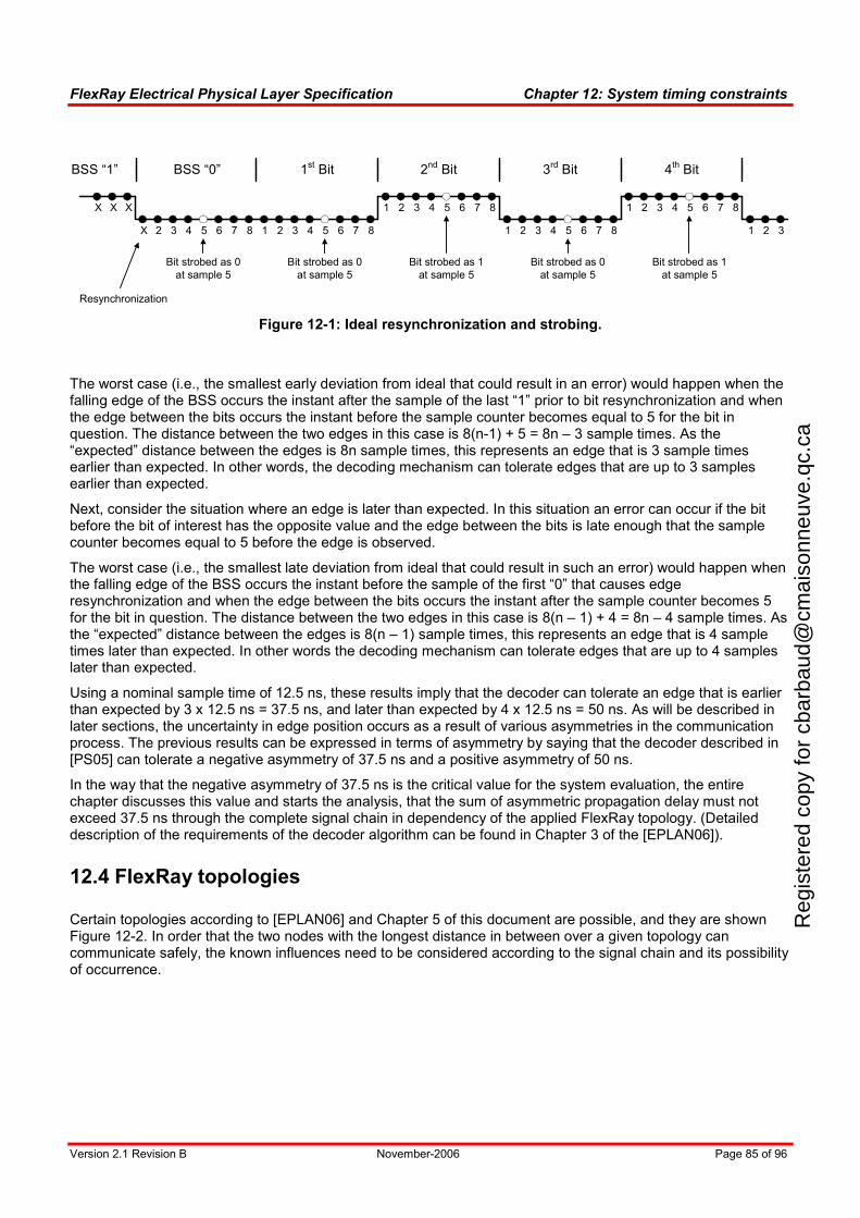
FlexRay Electrical Physical Layer Specification Chapter 12: System timing constraints
Version 2.1 Revision B November-2006 Page 85 of 96
BSS “0”
X X X
BSS “1”
X 2 3 4 5 6 7 8 1 2 3 4 5 6 7 8 1 2 3 4 5 6 7 8
1 2 3 4 5 6 7 8 1 2 3 4 5 6 7 8
1 2 3
1st Bit 2
nd Bit 3
rd Bit 4
th Bit
Resynchronization
Bit strobed as 0
at sample 5
Bit strobed as 0
at sample 5
Bit strobed as 1
at sample 5
Bit strobed as 0
at sample 5
Bit strobed as 1
at sample 5
Figure 12-1: Ideal resynchronization and strobing.
The worst case (i.e., the smallest early deviation from ideal that could result in an error) would happen when the falling edge of the BSS occurs the instant after the sample of the last “1” prior to bit resynchronization and when the edge between the bits occurs the instant before the sample counter becomes equal to 5 for the bit in question. The distance between the two edges in this case is 8(n-1) + 5 = 8n – 3 sample times. As the “expected” distance between the edges is 8n sample times, this represents an edge that is 3 sample times earlier than expected. In other words, the decoding mechanism can tolerate edges that are up to 3 samples earlier than expected.
Next, consider the situation where an edge is later than expected. In this situation an error can occur if the bit before the bit of interest has the opposite value and the edge between the bits is late enough that the sample counter becomes equal to 5 before the edge is observed.
The worst case (i.e., the smallest late deviation from ideal that could result in such an error) would happen when the falling edge of the BSS occurs the instant before the sample of the first “0” that causes edge resynchronization and when the edge between the bits occurs the instant after the sample counter becomes 5 for the bit in question. The distance between the two edges in this case is 8(n – 1) + 4 = 8n – 4 sample times. As the “expected” distance between the edges is 8(n – 1) sample times, this represents an edge that is 4 sample times later than expected. In other words the decoding mechanism can tolerate edges that are up to 4 samples later than expected.
Using a nominal sample time of 12.5 ns, these results imply that the decoder can tolerate an edge that is earlier than expected by 3 x 12.5 ns = 37.5 ns, and later than expected by 4 x 12.5 ns = 50 ns. As will be described in later sections, the uncertainty in edge position occurs as a result of various asymmetries in the communication process. The previous results can be expressed in terms of asymmetry by saying that the decoder described in [PS05] can tolerate a negative asymmetry of 37.5 ns and a positive asymmetry of 50 ns.
In the way that the negative asymmetry of 37.5 ns is the critical value for the system evaluation, the entire chapter discusses this value and starts the analysis, that the sum of asymmetric propagation delay must not exceed 37.5 ns through the complete signal chain in dependency of the applied FlexRay topology. (Detailed description of the requirements of the decoder algorithm can be found in Chapter 3 of the [EPLAN06]).
12.4 FlexRay topologies
Certain topologies according to [EPLAN06] and Chapter 5 of this document are possible, and they are shown Figure 12-2. In order that the two nodes with the longest distance in between over a given topology can communicate safely, the known influences need to be considered according to the signal chain and its possibility of occurrence.
Reg
iste
red
copy
for
cbar
baud
@cm
aiso
nneu
ve.q
c.ca
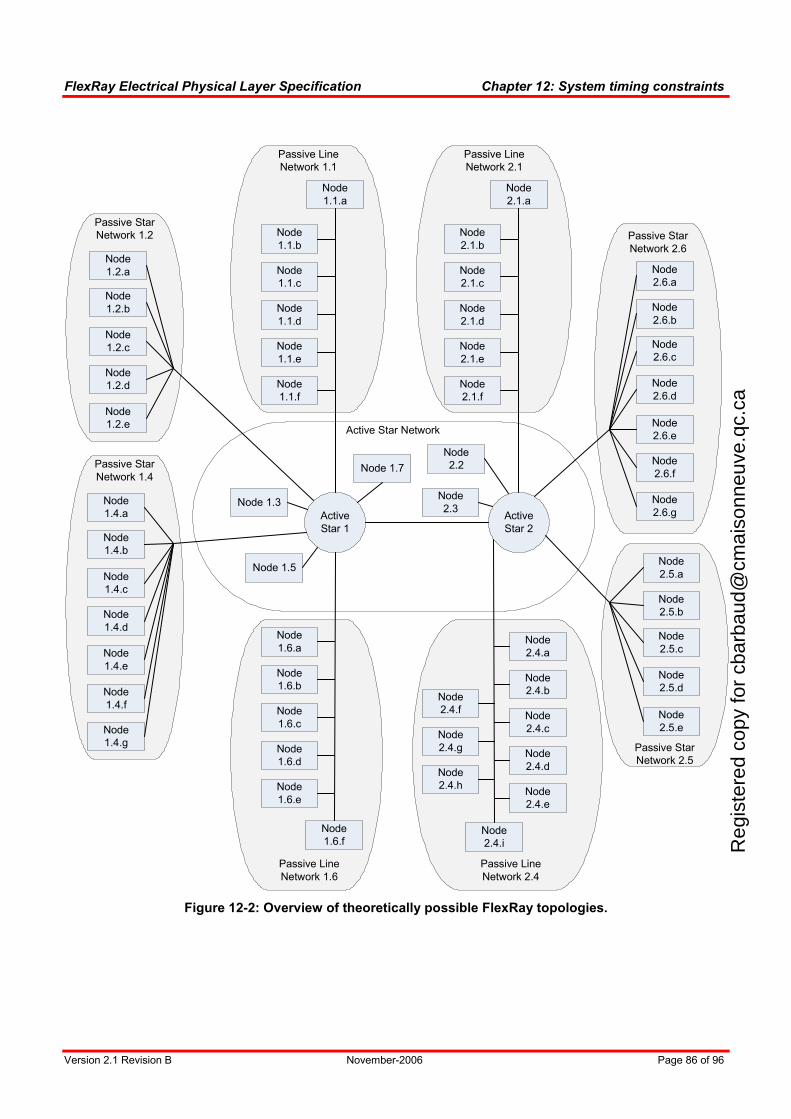
FlexRay Electrical Physical Layer Specification Chapter 12: System timing constraints
Version 2.1 Revision B November-2006 Page 86 of 96
Passive Star
Network 1.2
Passive Line
Network 1.1
Passive Star
Network 2.6
Node
2.6.g
Passive Line
Network 1.6
Active Star Network
Active
Star 1
Active
Star 2
Node 1.3
Node 1.5
Node
1.6.a
Node
1.6.b
Node
1.6.c
Node
1.6.d
Node
1.6.e
Node
1.6.f
Node
2.6.a
Node
2.6.b
Node
2.6.c
Node
2.6.d
Node
2.6.e
Node
2.6.f
Node
2.3
Node
2.2
Passive Line
Network 2.4
Node
2.4.a
Node
2.4.b
Node
2.4.c
Node
2.4.d
Node
2.4.e
Node
2.4.i
Node
2.4.f
Node
2.4.g
Node
2.4.h
Node 1.7
Node
1.1.b
Node
1.1.c
Node
1.1.d
Node
1.1.e
Node
1.1.f
Node
1.1.a
Node
1.2.a
Node
1.2.b
Node
1.2.c
Node
1.2.d
Node
1.2.e
Passive Star
Network 1.4
Node
1.4.a
Node
1.4.b
Node
1.4.c
Node
1.4.d
Node
1.4.e
Node
1.4.f
Node
1.4.g
Passive Line
Network 2.1
Node
2.1.b
Node
2.1.c
Node
2.1.d
Node
2.1.e
Node
2.1.f
Node
2.1.a
Passive Star
Network 2.5
Node
2.5.a
Node
2.5.b
Node
2.5.c
Node
2.5.d
Node
2.5.e
Figure 12-2: Overview of theoretically possible FlexRay topologies.
Reg
iste
red
copy
for
cbar
baud
@cm
aiso
nneu
ve.q
c.ca
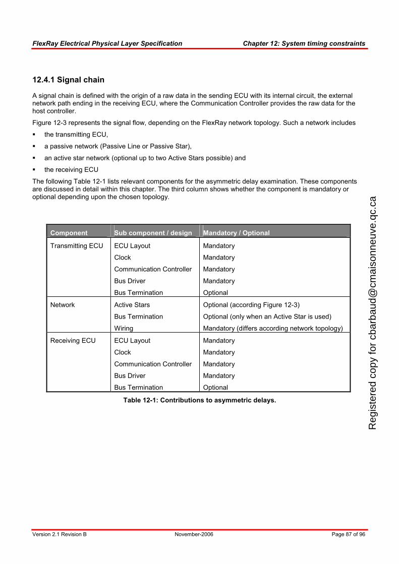
FlexRay Electrical Physical Layer Specification Chapter 12: System timing constraints
Version 2.1 Revision B November-2006 Page 87 of 96
12.4.1 Signal chain
A signal chain is defined with the origin of a raw data in the sending ECU with its internal circuit, the external network path ending in the receiving ECU, where the Communication Controller provides the raw data for the host controller.
Figure 12-3 represents the signal flow, depending on the FlexRay network topology. Such a network includes
the transmitting ECU,
a passive network (Passive Line or Passive Star),
an active star network (optional up to two Active Stars possible) and
the receiving ECU
The following Table 12-1 lists relevant components for the asymmetric delay examination. These components are discussed in detail within this chapter. The third column shows whether the component is mandatory or optional depending upon the chosen topology.
Component Sub component / design Mandatory / Optional
Transmitting ECU ECU Layout
Clock
Communication Controller
Bus Driver
Bus Termination
Mandatory
Mandatory
Mandatory
Mandatory
Optional
Network Active Stars
Bus Termination
Wiring
Optional (according Figure 12-3)
Optional (only when an Active Star is used)
Mandatory (differs according network topology)
Receiving ECU ECU Layout
Clock
Communication Controller
Bus Driver
Bus Termination
Mandatory
Mandatory
Mandatory
Mandatory
Optional
Table 12-1: Contributions to asymmetric delays.
Reg
iste
red
copy
for
cbar
baud
@cm
aiso
nneu
ve.q
c.ca
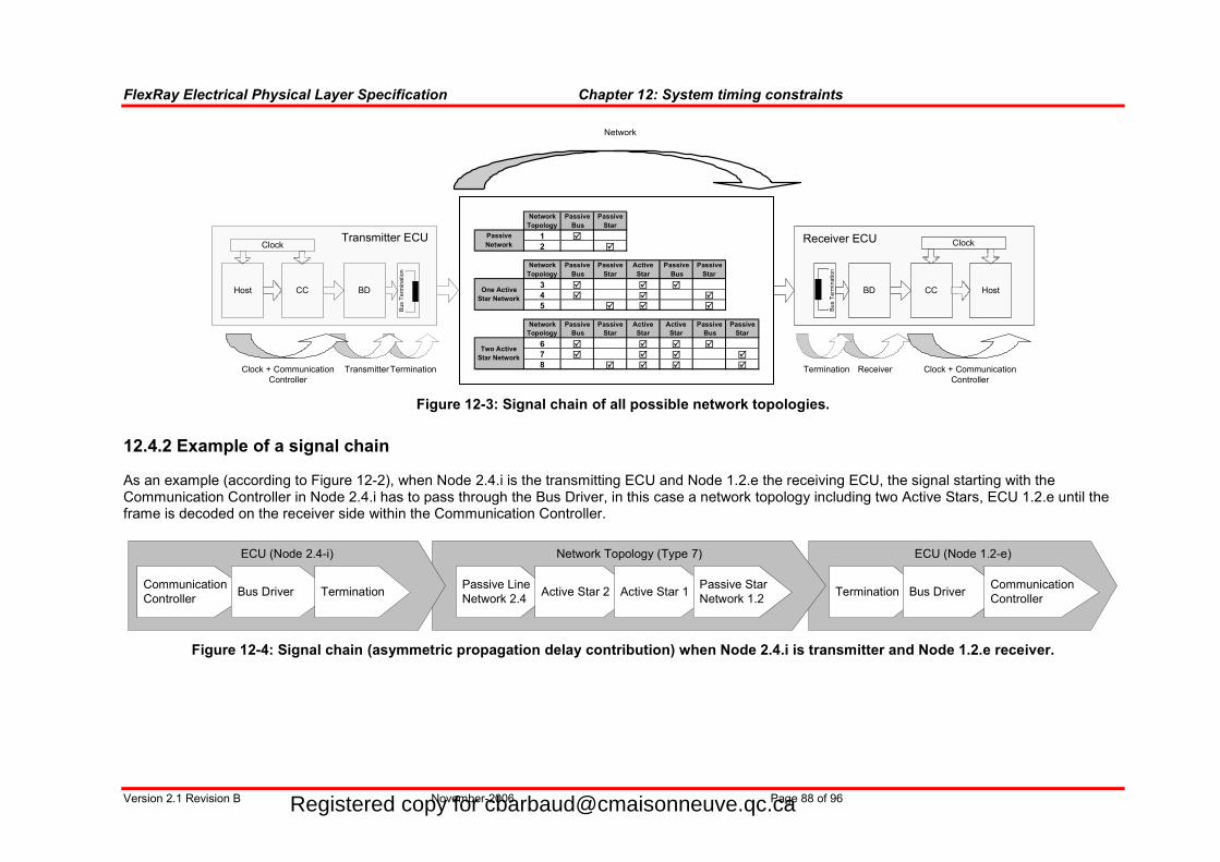
FlexRay Electrical Physical Layer Specification Chapter 12: System timing constraints
Version 2.1 Revision B November-2006 Page 88 of 96
Receiver
Termination
Transmitter
Clock + Communication
Controller
Network
Receiver ECU
CCBD Host
Bu
s T
erm
ination
ClockTransmitter ECU
CC BDHost
Bus T
erm
ination
Clock
Network
Topology
Passive
Bus
Passive
Star
1
2
Network
Topology
Passive
Bus
Passive
Star
Active
Star
Passive
Bus
Passive
Star
3
4
5
Network
Topology
Passive
Bus
Passive
Star
Active
Star
Active
Star
Passive
Bus
Passive
Star
6
7
8
Passive
Network
One Active
Star Network
Two Active
Star Network
Termination
Clock + Communication
Controller
Figure 12-3: Signal chain of all possible network topologies.
12.4.2 Example of a signal chain
As an example (according to Figure 12-2), when Node 2.4.i is the transmitting ECU and Node 1.2.e the receiving ECU, the signal starting with the Communication Controller in Node 2.4.i has to pass through the Bus Driver, in this case a network topology including two Active Stars, ECU 1.2.e until the frame is decoded on the receiver side within the Communication Controller.
ECU (Node 1.2-e)Network Topology (Type 7)
Passive Line
Network 2.4Active Star 2 Active Star 1
ECU (Node 2.4-i)
Communication
ControllerBus Driver Termination
Passive Star
Network 1.2Termination Bus Driver
Communication
Controller
Figure 12-4: Signal chain (asymmetric propagation delay contribution) when Node 2.4.i is transmitter and Node 1.2.e receiver.
Registered copy for [email protected]
FlexRay Electrical Physical Layer Specification Chapter 12: System timing constraints
Version 2.1 Revision B November-2006 Page 89 of 96
Summing up all possible topologies considering a maximum of two Active Stars, 8 different combinations of network topologies are possible with different signal chains according to the topology.
It is assumed, that a point-to-point connection does not bring additional asymmetric delay into the signal chain, but as passive line networks cannot be implemented with stub lengths zero, those network topologies need to considered in the overall network topology evaluation as shown in Figure 12-3.
In the following chapters contributions on asymmetric propagation delays are described in detail. The host controller contribution is not discussed in this chapter, because it is assumed that ECU internal interfaces are already captured in the ECU layout and digital connections, with only raw data interaction contributing additional asymmetric delays.
12.5 Description of asymmetry portions
12.5.1 Communication Controller
12.5.1.1 Oscillator tolerance
The sample clocks used by transmitting and receiving Communication Controller to generate and sample the bit stream are derived from oscillators local to the node. Because of oscillator tolerances, the sample clock oscillator of the transmitter may run at a different frequency than the sample clock oscillator of the receiver. This rate difference will result in a systematic error in the perception of the incoming sample stream, and this error contributes to the overall asymmetry of the system.
A fast oscillator in a transmitter will make edges appear to arrive earlier than expected with respect to the falling edge of the BSS. A slow oscillator in the transmitter will make the edges arrive later than expected. The situation is basically opposite in the receivers – a fast oscillator makes the edges appear to arrive late, and slow oscillator will make the edges appear to arrive early.
The worst case for early edges is when the transmitter oscillator is at its tolerance limit on the fast side, and the receiver oscillator is at its tolerance limit on the slow side. The worst case for late edges is when the transmitter oscillator is at its tolerance limit on the slow side, and the receiver oscillator is at its tolerance limit on the fast side.
The magnitude of the effect is also a function of how far the edge occurs away from the resynchronization at the falling edge of the BSS. The effect is larger for edges further away from the falling edge of the BSS.
12.5.1.2 Sampling clock accuracy
Clock accuracy with PLL A phase locked loop (PLL) can be used to provide the required sample clock based on a lower frequency. The PLL jitter influences both the transmitting and receiving Communication Controller.
Clock accuracy without PLL One way to minimize signal asymmetries is the use of a clock source, which is 16-times the bit frequency. The usage of a clock source, 8 times the bit frequency, by using rising and falling edges generates also the recommended clock, but may introduce additional asymmetry because of a non-ideal duty cycle. The amount of asymmetry depends on the duty cycle directly but increases the static asymmetry only at the receiving side.
Reg
iste
red
copy
for
cbar
baud
@cm
aiso
nneu
ve.q
c.ca
FlexRay Electrical Physical Layer Specification Chapter 12: System timing constraints
Version 2.1 Revision B November-2006 Page 90 of 96
12.5.1.3 Generic digital component contribution
Setup & hold times The setup and the hold times are not considered separately because these values are included in worst case considerations of time discretization of the sampling process. The considered time discretization is greater than any setup time. If there is any hold time in semiconductor process, it will be present both at synchronizing the sampling clock and at sampling point. Both hold times neutralize each other.
I/O buffer Complementary transistors of I/O buffers never match perfect. Thus, a propagation delay mismatch might occur. These asymmetries will vary with temperature and supply voltage variations, but are assumed to be constant during the reception of one frame.
Pin pad The pin pads of the Communication Controllers within the semiconductor device may be a source of static asymmetric delay because of different locations of different pin pads on the chip and because of production tolerances. The pin pad will not insert a stochastic asymmetry. The output pins of a Communication Controller will typically have slew rate controlled pin pads in order to limit the electromagnetic emission. Slew rate for rising and falling edges might not match. In fact a positive asymmetric delay can be assumed since it is expected that the pull-down transistor is faster than the pull-up transistor.
12.5.2 Contribution of the Bus Driver
12.5.2.1 Transmitter
The transmitter is part of the Bus Driver and describes in the signal chain the sender, which generates from the TxD digital input the specified bus signals on the BP and BM lines (for more details refer to EPL Application Notes).
Below are listed effects to asymmetric propagation delays of the transmitter:
The transmitter consists of a high side driver (pull up) and a low side driver (pull down) for the BP line as well as the BM line. This architecture only can guarantee the symmetry in a specified range of the voltages on BP and BM lines respect the VDD/2 level. Same effects apply also during the transition phases of the bus states.
Control mechanism of edges is not fully symmetrical. Due to current consumption reduction and two different output drivers (N; P) a fully symmetrically edge control cannot be met.
With respect to the input signal of TxD and the dependency on the slew rates of rising and falling edges, the output stage is transmitting accordingly the bit times on the bus.
12.5.2.2 Receiver
The receiver is part of the Bus Driver and describes in the signal chain the recipient, which generates from the analog bus signals on BP and BM, the appropriate digital RxD signal (for more details refer to EPL Application Notes).
Below are listed effects to asymmetric propagation delays of the receiver:
Slew rates of rising and falling edges are different on the RxD output.
Receiving hysteresis for digital conversion implemented. Those thresholds due the voltage range may be different.
12.5.2.3 Active Star
Same effects as for the Transmitter and Receiver apply for the Active Star contribution to the asymmetric propagation delay. But due to the implementation of the integrated active coupling functionality, it is assumed that the sum of asymmetric propagation delay in an Active Star is approximately the sum of asymmetric propagation delay in Receiver and Transmitter Bus Driver.
Reg
iste
red
copy
for
cbar
baud
@cm
aiso
nneu
ve.q
c.ca
FlexRay Electrical Physical Layer Specification Chapter 12: System timing constraints
Version 2.1 Revision B November-2006 Page 91 of 96
12.5.3 Interface between the Bus Driver and Communication Controller
The interface between the Bus Driver and the Communication Controller comprises as contribution to the overall asymmetric delay contribution in a way, that a mismatch of slew rates of both devices causes a delay and even the routing of the PCB wires between those 2 devices.
12.5.3.1 Interface from Communication Controller to Bus Driver (sending node)
Even the asymmetric delay contribution is caused by the interface between the Communication Controller and the Bus Driver, in case of the sending node, this contribution can firstly be observed after or in the Bus Driver and it appears as a contribution of the Bus Driver.
12.5.3.2 Interface from Bus Driver to Communication Controller (receiving node)
As in the sending node, the asymmetric delay contribution is caused by the interface between the Bus Driver and the Communication Controller in the receiving node, this contribution can firstly be observed after or in the Communication Controller and it appears as a contribution of the Communication Controller device.
Effects of interconnections between semiconductor devices on a PCB can be described with a micro strip line.
12.5.4 Passive networks
The receiver meets the “receiver data timing requirements” given in Table 8-18 when being stimulated by the “receiver input test signal …” according Table 8-19. This signal can be achieved in point-to-point and in daisy-chain passive networks. Passive stars are going to generate signals at the receiving bus-drivers, which do not match with this test signal. The expected signal shape will produce an additional asymmetric delay when passing a bus-driver. The worst-case signal shape is represented by a signal with a partly reduced slew-rate. This effect can be produced by reflections on the wires. If the reduced slew-rate area is located nearby the thresholds of the receiver and the thresholds have the maximum miss matching a maximized asymmetric delay is generated.
12.5.4.1 Point to point
The asymmetric delay is hidden in the asymmetric delay of the BD receiver. An additional asymmetric delay cannot be seen, the expected signal shape corresponds with the specified test signal.
12.5.4.2 Linear passive bus
A linear passive bus network with almost zero length to the connected stub-nodes (daisy chain) will have the same impact on the asymmetric delay contribution as a point to point network. In a real application, a linear passive bus with short stub lengths to the bus wiring, will have an impact on the overall systems asymmetric delay, which is assumed to be somewhere in between of a point to point and a maximum net consideration.
12.5.4.3 Passive star (maximum net)
Especially in passive star networks, additional static asymmetric delay when passing the receiving bus-driver is added, due to the slew-rate variations and due to maximal receiver threshold mismatches.
Reg
iste
red
copy
for
cbar
baud
@cm
aiso
nneu
ve.q
c.ca
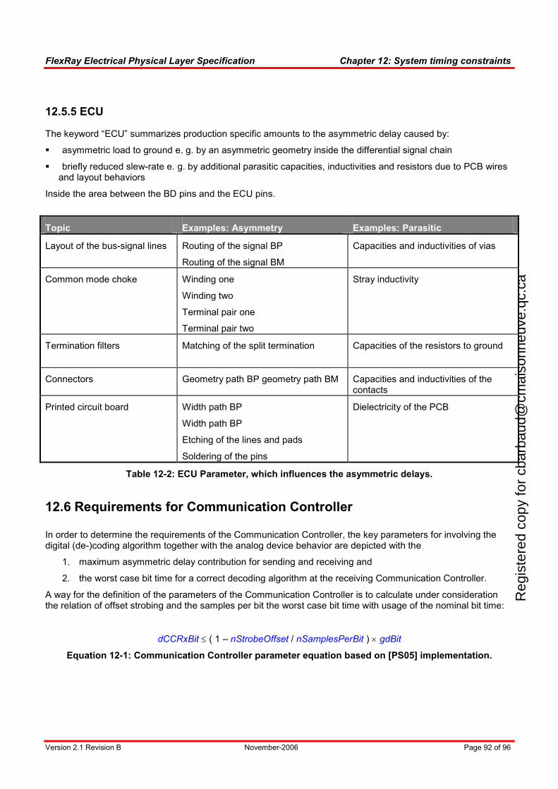
FlexRay Electrical Physical Layer Specification Chapter 12: System timing constraints
Version 2.1 Revision B November-2006 Page 92 of 96
12.5.5 ECU
The keyword “ECU” summarizes production specific amounts to the asymmetric delay caused by:
asymmetric load to ground e. g. by an asymmetric geometry inside the differential signal chain
briefly reduced slew-rate e. g. by additional parasitic capacities, inductivities and resistors due to PCB wires and layout behaviors
Inside the area between the BD pins and the ECU pins.
Topic Examples: Asymmetry Examples: Parasitic
Layout of the bus-signal lines Routing of the signal BP
Routing of the signal BM
Capacities and inductivities of vias
Common mode choke Winding one
Winding two
Terminal pair one
Terminal pair two
Stray inductivity
Termination filters Matching of the split termination Capacities of the resistors to ground
Connectors Geometry path BP geometry path BM Capacities and inductivities of the contacts
Printed circuit board Width path BP
Width path BP
Etching of the lines and pads
Soldering of the pins
Dielectricity of the PCB
Table 12-2: ECU Parameter, which influences the asymmetric delays.
12.6 Requirements for Communication Controller
In order to determine the requirements of the Communication Controller, the key parameters for involving the digital (de-)coding algorithm together with the analog device behavior are depicted with the
1. maximum asymmetric delay contribution for sending and receiving and
2. the worst case bit time for a correct decoding algorithm at the receiving Communication Controller.
A way for the definition of the parameters of the Communication Controller is to calculate under consideration the relation of offset strobing and the samples per bit the worst case bit time with usage of the nominal bit time:
dCCRxBit ≤ ( 1 – nStrobeOffset / nSamplesPerBit ) × gdBit
Equation 12-1: Communication Controller parameter equation based on [PS05] implementation.
Reg
iste
red
copy
for
cbar
baud
@cm
aiso
nneu
ve.q
c.ca
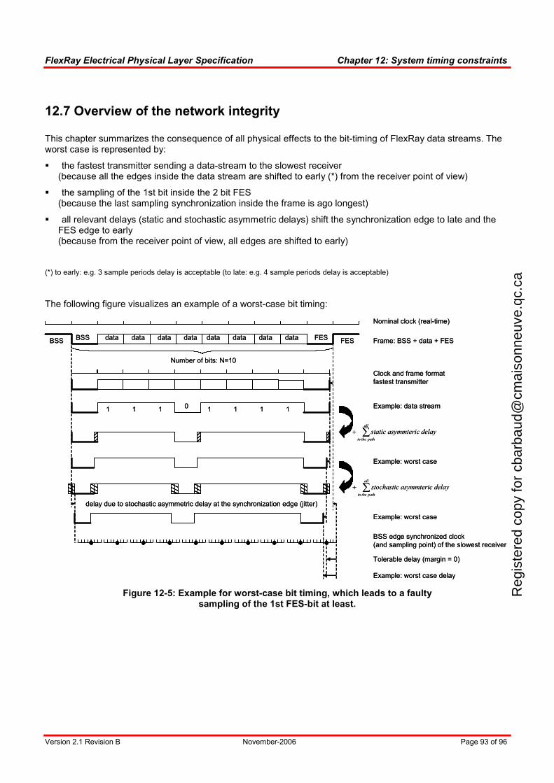
FlexRay Electrical Physical Layer Specification Chapter 12: System timing constraints
Version 2.1 Revision B November-2006 Page 93 of 96
12.7 Overview of the network integrity
This chapter summarizes the consequence of all physical effects to the bit-timing of FlexRay data streams. The worst case is represented by:
the fastest transmitter sending a data-stream to the slowest receiver (because all the edges inside the data stream are shifted to early (*) from the receiver point of view)
the sampling of the 1st bit inside the 2 bit FES (because the last sampling synchronization inside the frame is ago longest)
all relevant delays (static and stochastic asymmetric delays) shift the synchronization edge to late and the FES edge to early (because from the receiver point of view, all edges are shifted to early)
(*) to early: e.g. 3 sample periods delay is acceptable (to late: e.g. 4 sample periods delay is acceptable)
The following figure visualizes an example of a worst-case bit timing:
Frame: BSS + data + FES
Clock and frame format
fastest transmitter
BSS edge synchronized clock
(and sampling point) of the slowest receiver
Nominal clock (real-time)
Example: worst case
Tolerable delay (margin = 0)
Example: worst case delay
Number of bits: N=10
BSS dataBSS FES FESdata data data data data data data
delay due to stochastic asymmetric delay at the synchronization edge (jitter)
Example: data stream
∑+all
paththein
delayasymmtericstatic
∑+all
paththein
delayasymmtericstochastic
Example: worst case
1 1 1 0 1 1 1 1
Figure 12-5: Example for worst-case bit timing, which leads to a faulty sampling of the 1st FES-bit at least.
Reg
iste
red
copy
for
cbar
baud
@cm
aiso
nneu
ve.q
c.ca
FlexRay Electrical Physical Layer Specification Chapter 12: System timing constraints
Version 2.1 Revision B November-2006 Page 94 of 96
Topic 1
The end of a FlexRay frame has to be transmitted (based on a nominal clock):
2 bit BSS with one data-byte followed by the 2 bit FES
Topic 2
The transmitter with the fastest clock transmits the frame with an exemplary data
11101111 the edge inside the FES is shifted to early
Topic 3
On the path from the transmitter to the receiver (through the complete signal chain) the data stream timing is going to be deformed statically (static asymmetric delay, constant inside the frame)
E.g. a BD is allowed deform the bit-timing up to 4 ns statically
Topic 4
The worst case is represented by shifting the edges to early maximal
Topic 5
On the path from the transmitter to the receiver (through the complete channel) the data stream timing is going to be deformed stochastically (stochastic asymmetric delay, varied from edge to edge uncorrelated)
e. g. the bit-clock inside the transmitter could jitter a few ns from edge to edge
Topic 6
The worst case is represented by shifting the FES edge to early
and
by shifting the BSS edge to late (the receiver uses this edge for the sampling re-synchronization)
Topic 7
The receiver with the slowest clock samples the data-stream based on:
1. re-synchronized on the detected BSS-edge
2. using 8-time over-sampling (the implemented glitch filter does not influence the scenery)
3. using the 5th sample inside a bit as the only resulting sample point
Topic 8
A perfect sampling is guaranteed, if the FES edge is shifted up to the sampling point at most
a faulty sampling is guaranteed, if the FES edge is shifted before the sampling point at least
Reg
iste
red
copy
for
cbar
baud
@cm
aiso
nneu
ve.q
c.ca
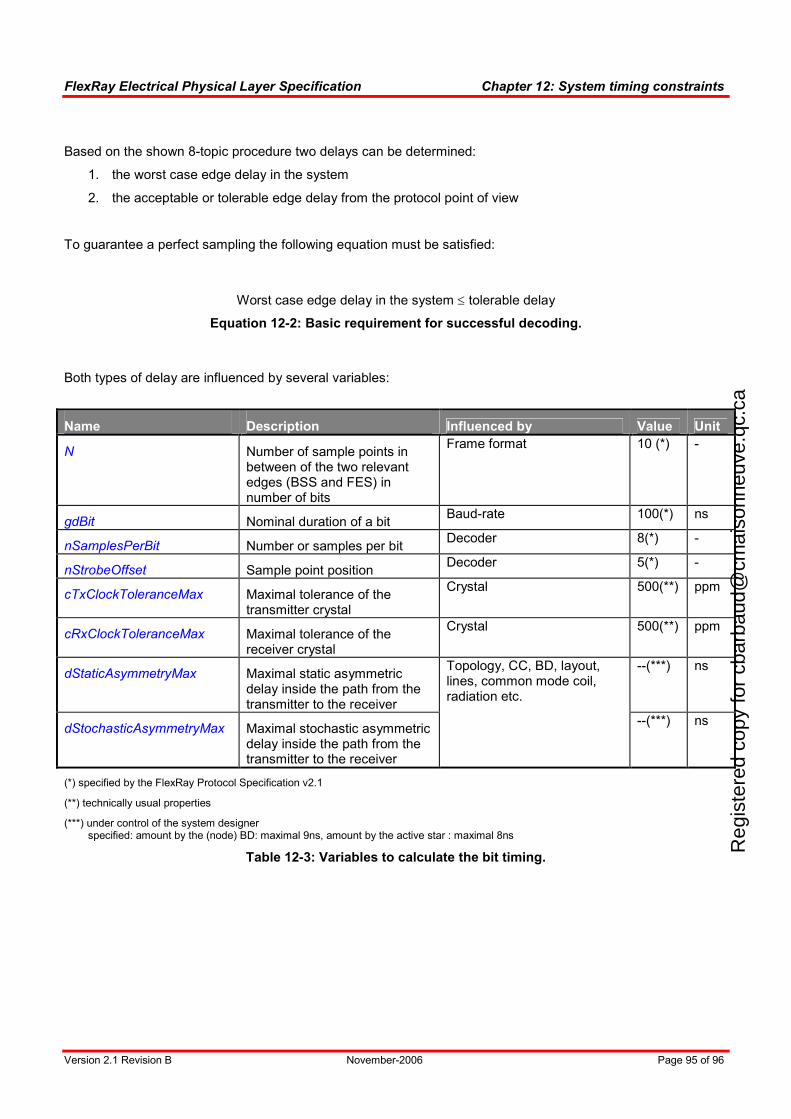
FlexRay Electrical Physical Layer Specification Chapter 12: System timing constraints
Version 2.1 Revision B November-2006 Page 95 of 96
Based on the shown 8-topic procedure two delays can be determined:
1. the worst case edge delay in the system
2. the acceptable or tolerable edge delay from the protocol point of view
To guarantee a perfect sampling the following equation must be satisfied:
Worst case edge delay in the system ≤ tolerable delay
Equation 12-2: Basic requirement for successful decoding.
Both types of delay are influenced by several variables:
Name Description Influenced by Value Unit
N Number of sample points in between of the two relevant edges (BSS and FES) in number of bits
Frame format 10 (*) -
gdBit Nominal duration of a bit Baud-rate 100(*) ns
nSamplesPerBit Number or samples per bit Decoder 8(*) -
nStrobeOffset Sample point position Decoder 5(*) -
cTxClockToleranceMax Maximal tolerance of the transmitter crystal
Crystal 500(**) ppm
cRxClockToleranceMax Maximal tolerance of the receiver crystal
Crystal 500(**) ppm
dStaticAsymmetryMax Maximal static asymmetric delay inside the path from the transmitter to the receiver
--(***) ns
dStochasticAsymmetryMax Maximal stochastic asymmetric delay inside the path from the transmitter to the receiver
Topology, CC, BD, layout, lines, common mode coil, radiation etc.
--(***) ns
(*) specified by the FlexRay Protocol Specification v2.1
(**) technically usual properties
(***) under control of the system designer specified: amount by the (node) BD: maximal 9ns, amount by the active star : maximal 8ns
Table 12-3: Variables to calculate the bit timing.
Reg
iste
red
copy
for
cbar
baud
@cm
aiso
nneu
ve.q
c.ca
FlexRay Electrical Physical Layer Specification Chapter 12: System timing constraints
Version 2.1 Revision B November-2006 Page 96 of 96
The delays can be calculated very easily by adding all influences. Equation 12-2 becomes to:
Worst case edge delay in the system
gdBit x N x cTxClockToleranceMax
+ gdBit x N x cRxClockToleranceMax
+ dStaticAsymmetryMax
+ dStochasticAsymmetryMax ≤
Tolerable delay
gdBit x (1 - nStrobeOffset / nSamplesPerBit)
The equation is simplified: e.g. non-linear parts like cTxClockToleranceMax² are neglected
Equation 12-3:.
The equation has 4 constants which are pre-defined by the FlexRay protocol, 2 variables can be controlled by the system designer easily (see: crystals) and just 2 variables are influenced by various parameters: dStaticAsymmetryMax and dStochasticAsymmetryMax.
By taking the fixed parameter into account, the system designer has to meet the requirements shown in the next equation:
dStaticAsymmetryMax
+ dStochasticAsymmetryMax
≤
gdBit x (1-nStrobeOffset / nSamplesPerBit)
- gdBit x N x cTxClockToleranceMax
- gdBit x N x cRxClockToleranceMax
Equation 12-3a:.
Explaining the clock tolerance:
2 x gdBit x N x cRxClockToleranceMax = 2 x 100ns x 10 x 500ppm
= 1ns
= 1% x gdBit
Equation 12-4:.
By using the values of the Table 12-3:
dStaticAsymmetryMax + dStochasticAsymmetryMax ≤ gdBit x ( 3/8 - 1%)
= gdBit x 0.365
Equation 12-3b:.
Name 2.5 Mbit/s 5 Mbit/s 10 Mbit/s Unit
dStaticAsymmetryMax + dStochasticAsymmetryMax 146 73 36.5 ns
Table 12-4: Overview of the asymmetric delay requirements when using 500ppm crystals in a FlexRay system [PS05].
=== END OF DOCUMENT ===
Reg
iste
red
copy
for
cbar
baud
@cm
aiso
nneu
ve.q
c.ca
![The Message Scheduling Methods of FlexRay ...that FlexRay involves the additional concepts of active star and passive star [9]. FlexRay is also appropriate for critical and real-time](https://img.pdfslide.us/doc/110x75/60854139a57328728b0c50ed/the-message-scheduling-methods-of-flexray-that-flexray-involves-the-additional.jpg)


![Electrical Physical Layer Application Notes - svn.ipd.kit.eduE2%84%A2%20... · [EMC10] FlexRay Communication System – Electrical Physical Layer EMC measurement specification, Version](https://img.pdfslide.us/doc/110x75/5a79c96a7f8b9ab05f8c6047/electrical-physical-layer-application-notes-svnipdkitedu-e284a220emc10.jpg)