Embed Size (px)
Citation preview

Flexfilm – A Novel Film-based MID Process
Dr -Ing Marcus Schuck1Dr.-Ing. Marcus SchuckProf. Dr.-Ing. Dietmar Drummer2
Dipl.-Ing. Andreas Seefried2
Di l Wi t h I Mi h l F h 2Dipl.-Wirtsch.-Ing. Michael Fuchs2
1 Jacob Plastics GmbH 2 Institute of Polymer TechnologyJacob Plastics GmbH
Bergstraße 31 - 3591489 Wilhelmsdorf D t hl d / G
Institute of Polymer Technology
Am Weichselgarten 991052 Erlangen D t hl d / GDeutschland / Germany
Tel.: +49 (0)9104 / 8270-492Fax: +49 (0)9104 / [email protected]
Deutschland / GermanyTel.: +49 (0)9131 / 85297-00Fax: +49 (0)9131 / [email protected]
1
www.jacob-kunststofftechnik.de
[email protected] erlangen.de
www.lkt.uni-erlangen.de

Content
Motivation and GoalsPerformance potential Flexfilm– Performance potential Flexfilm
– Application potential Flexfilm
Process chain Flexfilm– Film extrusion
Hot embossing– Hot embossing
– Radiation cross linking
– Thermoforming
– Injection molding
– SMD assembly
Outlook
2
Summary

Applications of polymer films
Decorative films Flexiblecircuits
Packagingfilms
[Schlenk]
Market development flexible circuitsMarket development flexible circuitsexample: automobile
FFC: flexible flat cablesFPC: flexible printed circuits
market volume
estimated market volume EU 2008:FPC: 300 Mio. €FFC 1200 Mi €
FPC: flexible printed circuits
3
[Freudenberg]
FFC: 1200 Mio. €

Motivation and GoalsState of the art
4

Motivation and GoalsPerformance potential Flexfilm
Application of radiation cross linked technical thermoplastics as filmthermoplastics as film material for flexible printed circuit boards
3D MIDthree dimensional formability via thermoforming+
5
3D-MID(multi layer)large-area bonding via injection molding+

Motivation and GoalsApplication potential Flexfilm
Rigid/Flex-Interconnections
connector SMD[Lucent]
Appliction of 2D-
[capicard]
Appliction of 2D-Metallization techniquesinjection molded
substrate
conductor pathMulti layer MID
(with through connections)
[Lucent]
6film

BasicsRadiation cross linking
Non Cross LinkedSemi Crystalline Polymer
Radiation Cross LinkedSemi Crystalline Polymer
Complete Melting for T > Tm
Rubber-elasticBehavior for T > Tm
us
non cross linkedcross linked
soldering temperature
li k d t ung’
s m
odul
radiation cross linked part
7
non cross linked part, PA6-GF30, after lead-free soldering (Tmax = 255 °C, 10 min)
You
Tg TmRT
radiation cross linked part, PA6-GF30, after lead-free soldering (Tmax = 255 °C, 10 min)

Process chain Flexfilm
CriteriaAdhesion of metallizationThermal expansionThermoformabilityThermoformabilityAdhesion in injection moldingSolderabilitySolderability
8
One of the central research targets was to find the optimal time for radiation cross linking within the process chain.

Film extrusionFilm thickness
PBT, film extrusion with chill-roll
driving speed
ess
[µm
]fil
m th
ickn
e
pull-off speed [m/min]
9
High quality films with thicknesses from200 µm to 600 µm can be extruded.

Material choice and film extrusion
Radiation cross linkable PBT is commercially available and can be extruded to films.
Film extrusion of cross linkable, semi crystalline thermoplastics
ResinPBT V-PTS-Createc-B3HZC
Film extrusionCollin ESE E30M
Film (radiation cross linkable)Thickness 300 µm
Lifocolor COLCOLOR E40/601 Weight-%
Flat film die 250 °CChill-roll 80 °C
Pull off speed
Thickness 300 µm Width 220 mm
10
Pull-off speed1.8 m/min

Hot embossingProcess windows for metallization
12
experimental stamp layout
0,512
3
50
peel testp(according to DIN 53494)
pull-off speed: 50 mm/min
copper strip
polymer film
F
roll (∅ 5 mm)Widening of specific hot embossing process window can be reached withdi ti li ki d t h d th h i l i t
30 mm test length
radiation cross linking due to enhanced thermo-mechanical resistance.Peel resistances up to 2.5 N/mm may be detected which are mainlyinfluenced by embossing stamp temperature as key process factor.
11

Radiation Cross LinkingInfluence on Mechanical Film Properties
Specimen Type 5ASpecimen Type 5A
Testing climateTesting climatetemperature 23 °C, 50 % rel. humidity
Test velocityTest velocity15 mm/min
Tensile Test (according to DIN ISO 527)
12
(according to DIN ISO 527)

Metallization and Structuring
Radiation cross linkable PBT-films can be metallized with strip lines cost-effectively by hot embossing, fulfilling the demands of high adhesive force at the same time.
Hot embossing onto thermoplastic film substrates
same time.
Film (radiation cross linkable)Thickness 300 µm
Film (circuit)18 µm Copper + BlackOxide+ Surface finishing (Tin)
Hot embossingPress system (Blue Tiger Systems) Radiation
Width 220 mm
13
Embossing temperature 183°CEmbossing pressure 33 N/mm²Embossing time 0,5 sec
cross linkingElectron energy 5 MeVDose 5 x 33kGy

ThermoformingThermoformability of metallization
linear draw ratio Rl angle αi
1.10 65.4°1.15 60.4°1 20 56 4°
Thermoformingmold geometry
1.20 56.4°1.25 53.1°1.30 50.3°1.40 45.6°
metallization18 µm Cu + BlackOxide
elongationincrease
Elongation at break is ca 2 5 % at 200 °C for the copper foil linear draw ratio in thermoformed parts up to 140
PBT, 600 µm, 5 x 33 kGypainted, without metallizationTU = 230 °Cαi: 56.44 °, Rl = 1.20
PBT, 600 µm, 5 x 33 kGypainted, with metallizationTU = 230 °Cαi: 56.44 °, Rl = 1.20
14
Elongation at break is ca. 2.5 % at 200 C for the copper foil, linear draw ratio in thermoformed parts up to 140 % can be reached with hot embossed films.Due to an elongation increase of the polymer film, greater strains than the copper foil’s elongation at break may be reached by thermoforming metallizied films.

Shape Forming and Cutting
Thermoforming of PBT-films prior to the radiation cross linking is not possible, but after the cross linking step film substrates featured with necessary forming properties.
Thermoforming of metallized film substrates
properties.
Thermoformed insertThermoformingFilm (circuit) Thermoformed insertVarious deformation degreesSteepest edge 45,6°
ThermoformingBerg Mini M3Temperature of semi-finished part 240 °CMold temperature 40 °C
Film (circuit)18 µm Copper + BlackOxide + Surface finish (Tin)Dose 5 x 33kGy
15
Mold temperature 40 CVacuum

Injection moldingFilm adhesion
Film materialPBT
V-PTS-Createc B3HZC
Injection molding resinPBT
V-PTS-Createc B3HZC
Injection molding geometry
16

Injection molding
Injection molding - mold
Multiple cartridge mold to adjust backmolding geometry to test quality of
1 Adh i b t fil d i d
17
1. Adhesion between film and resin and 2. Soldering resistance

Injection molding
Injection molding film + structure
Thermoformed insert
Different draw ratiosSteepest edge 45.6°
Injection moldingFerromatik Millacron 110t
Melt temperature 295°C
Injection molded multi-component part
Injection molded,
18
Steepest edge 45.6 Melt temperature 295 CMold temperature 80°C
Injection molded, thermoformed, cross linked film
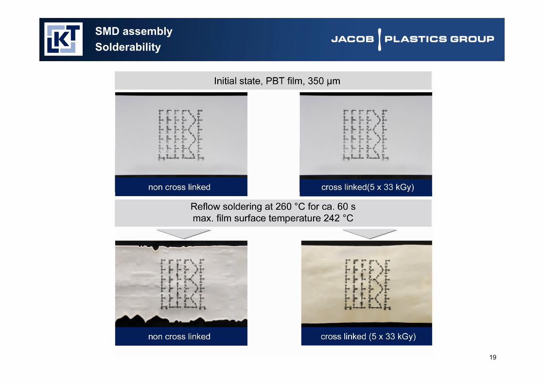
SMD assemblySolderability
19

OutlookFlexfilm
Further possibilities for development steps:– Combined use of copper-clad films and subtractive
structuring processes
Two sided metallization with through connection– Two-sided metallization with through connection
– Thermoforming of entire flexible printed circuits
– Realization of Rigid/Flex interconnections
20

SummaryFlexfilm process
With the process chain of Flexfilm three-dimensional interconnect devices can be produced by means of two-dimensional metallization and structuring processes.
Thus the Flexfilm process enables the manufacturing of multi layered MIDs.
Radiation cross linking may be conducted after film extrusion and has to be carried out at the last after metallization.E t i f di ti li k bl fil f t h i l i t lli th l tiExtrusion of radiation cross linkable films of technical semi crystalline thermoplastics is feasible.By hot embossing copper films onto the polymer substrate good adhesion can be achievedachieved.Thermoformability is greatly increased by radiation cross linking.Due to an elongation increase of the polymer film, greater strains than the copper foil’s l ti t b k b h d b th f i t lli d filelongation at break may be reached by thermoforming metallized films.
Sufficient adhesion to the film insert is achievable by injection molding.The temperature resistance of radiation cross linked films is sufficient for lead-free
f
21
reflow soldering.
Acknowledgment
Our special thanks go to:
Bayerisches Staatsministerium für Wirtschaft, Infrastruktur, Verkehr und Technologie for founding this work within the research project NW0707-0008 Entwicklung strahlenvernetzter Flexfolien inproject NW0707-0008 „Entwicklung strahlenvernetzter Flexfolien in Hybridgehäusen“ in the program „Neue Werkstoffe in Bayern“
FAPS Institute for Manufacturing Automation and Production Systems, Erlangen, Germany, for their support regarding SMD assemblyassembly
Beta Gamma Service, Saal a.d. Donau, Germany, for the electron beam irradiation of polymer films
22