Embed Size (px)
Citation preview

Computational Materials Science 81 (2014) 607–611
Contents lists available at ScienceDirect
Computational Materials Science
journal homepage: www.elsevier .com/locate /commatsci
First principles study of the voltage-dependent conductance propertiesof n-type and p-type graphene–metal contacts
0927-0256/$ - see front matter � 2013 Elsevier B.V. All rights reserved.http://dx.doi.org/10.1016/j.commatsci.2013.09.015
E-mail address: [email protected]
Serhan YamacliNuh Naci Yazgan University, Department of Electrical-Electronics Engineering, 38090 Kayseri, Turkey
a r t i c l e i n f o
Article history:Received 23 July 2013Received in revised form 3 September 2013Accepted 5 September 2013Available online 7 October 2013
Keywords:GrapheneMetal contactConductanceTransmission spectrum
a b s t r a c t
Investigation of the conductance properties of metal–graphene contacts is essential for the future nano-electronics technology. In this study, we focus on the conductance mechanism and the voltage-depen-dent transport properties of both p-type and n-type graphene–metal contacts. Copper and gold arechosen as the contact metal for n-type and p-type doped graphene–metal interface, respectively. Utiliz-ing first principles quantum mechanical calculations with density functional theory in conjunction withGreen’s function formalism, transmission spectra of graphene–metal contacts and the voltage-dependentvariations of the current and the resistance are obtained. Finally, it is shown that obtained resistance–voltage behaviours of graphene–metal contacts are in consistent with the results reported in the litera-ture and the voltage-dependency of the contact resistance has to be taken into consideration for thenanoscale circuit design process.
� 2013 Elsevier B.V. All rights reserved.
1. Introduction
Graphene is considered to be an advantageous candidate for thefuture nanoelectronics technology owing to its high electrical [1]and thermal conductivity [2], mechanical performance [3] and no-vel production methods [4]. Graphene is a zero-gap semiconductorwith a linear dispersion relationship near the K-point in the Brill-ouin zone [5]. Measured high carrier density of 3 � 1012 cm�2 [6]and the conductivity as high as conductance quantum [7], whichis the highest conductance per quantum channel at the nanoscale[8], enables to use graphene in nanoscale circuits as interconnects[9] and as the channels of graphene field effect transistors (FETs)[10]. Although graphene is internally a zero-gap ambipolar semi-conductor [11] with high mobility, its interaction with metals al-ters its electrical behaviour [12]. The contact of graphene withmetals is inescapable since various metallic interconnects are ex-pected to be present in the nanoscale electronic technology suchas aluminium, copper, gold, silver and platinum [13] which makecontacts with graphene. The effects of the different types of metalson the conductance properties of graphene–metal interface clearlyhave to be investigated in order to model these contacts accurately.
There are various studies treating the graphene–metal contactwith both theoretical and experimental discussions. Khomyakovet al. [14] investigated the doping of graphene with the contactmetal using first-principles methods. They found out that grapheneis doped either n-type or p-type when it comes into contact with ametal depending on the work function differences of graphene and
the contact metal. Metals which have lower work functions thangraphene dope graphene as n-type near the interface and vice ver-sa. Graphene is doped n-type with Al, Ag and Cu while Au and Ptdope graphene as p-type [14]. Liu et al. [15] studied graphene–me-tal contact preparation methods, asymmetric conductances andannealing effects. They also show that charge transfer betweenmetal and graphene dope graphene depending on the work func-tion differences and this leads to asymmetric conductance charac-teristics. Huard et al. [16] measured the electrical transport ofgraphene–metal interface for various geometries. They show thatthe asymmetry of graphene–metal contact conductance arisesfrom the pinning of the charge density in the graphene part. Nag-ashio et al. [17,18] also performed graphene–metal interface mea-surements with different metals such as Ni, Cr/Au and Ti/Au. Theyhave shown that the intrinsic conductance of graphene in graph-ene FETs is highly affected with the contact resistance and thegraphene–metal contact resistance is around 500–1000 X lm[17]. In another study, Stokbro et al. [19] modelled the contactresistance of graphene–nickel interface using first-principlesmethods and have shown that ab initio methods can be used tomodel graphene–metal contacts accurately. Barraza-Lopez et al.[20] studied graphene–aluminium contacts using ab initio simula-tions and obtained the potential profile at the interface to interpretcontact conductance. The temperature dependence of palladium–graphene contacts are investigated experimentally by Xia et al.[21] where mean-free path of electrons in graphene is used inthe modelling of the contact resistance. There are also other severalexperimental studies in the literature regarding the transportbehaviour of graphene–metal contacts. In one of these studies,

Fig. 1a. Simulated graphene–copper interface.
Fig. 1b. Simulated graphene–gold interface.
608 S. Yamacli / Computational Materials Science 81 (2014) 607–611
Heersche et al. investigated the resistance of graphene–supercon-ductor metal contacts and have given evidence of phase coherentelectronic transport [22]. Shot noise of graphene–metal interfacesare studied in [23,24]. Transport barriers at the metal–grapheneinterfaces are experimentally investigated in [25]. Russo et al.modelled charge transfer from the metal to graphene for severallayer graphene [26]. In another study, taking practical applicationsinto consideration, Robinson et al. implemented a method to pro-duce graphene–metal contacts with ultra-low resistance [27].The experimental measurements of the graphene–Pd contacts areperformed by Jiao et al. where it is found out that graphene isdoped p-type by Pd and there is an asymmetric resistance–voltagedependency [28]. Ballistic transport in graphene with metal con-tacts is discussed in the seminal paper of Novoselov et al. [29].The electrical measurements of field effect transistors, which usegraphene as the channel and various contact metals as the sourceand drain contacts, is another method to investigate the metal–graphene interfaces. In [30–32], this method is used to obtain thevariation of the graphene–metal contact resistance with thechange of the gate potential.
Experimental evidence of p-type doping of graphene in graph-ene–Au contacts is shown by Malec and Davidovic together withthe variation of the drain current by the gate voltage [33]. In an-other experimental study, n-type and p-type doping of graphenewith various metals is experimentally observed [34]. In [34],asymmetric resistance–voltage variation is also reported. Graph-ene–Cu contacts are experimentally studied in [35] showing thatgraphene is doped n-type with Cu and it is also shown thatannealing can increase contact conductivity. Knoch et al. utilizeddual-gate field effect transistor structure to measure graphene–metal contact properties. They found out that Pd contacts dopegraphene as p-type and extracted doping concentration fromexperiments [36].
Liu et al. used first-principles approach to investigate the con-tact resistance of graphene–Ni and graphene–Cu contacts and con-cluded that graphene–Ni contacts have lower conductance thangraphene–Cu contacts [37]. In [38], Do and Li considered the cou-pling between p-bands and sd bands and then modelled the resis-tance behaviours of graphene–metal contacts. Takagi and Okadaalso used first-principles methods to study the contacts of graph-ene with Pd, Au, Ag and Pt pillars and found out that the geometryof the contacts are also effective on the resistance value [39]. In[40], Barraza-Lopez et al. used DFT–NEGF transport calculationsof graphene–metal contacts with covalent bonds. In another study,tight-binding parameters for the dispersion curve of graphene–Ticontacts are obtained [41]. The self-energy parameters, which de-scribe graphene–metal coupling, is used to model the conductanceof graphene–metal interface in [42] and their model represents theasymmetric behaviour of the graphene–metal conductance. Maas-sen et al. used first-principles simulations to obtain the transportproperties of the contact of graphene with Cu(1,1,1) crystal andthey also found out that graphene is doped n-type by copper [43].
In this work, we investigate (i) voltage dependent transmis-sions, (ii) current–voltage variations and, (iii) voltage dependencyof the resistances of p-type and n-type graphene–metal contacts.Self-consistent quantum mechanical simulations employing den-sity functional theory (DFT) in conjunction with non-equilibriumGreen’s function formalism (NEGF) are used to obtain current–voltage variations of graphene–Cu and graphene–Au contacts.Voltage-dependent resistances of these graphene–metal contactsare then calculated. Asymmetry in their resistances is discussedand it is shown that obtained resistance behaviours are in consis-tent with the interpretations existing in the literature. Finally, apolynomial model for representing the current–voltage character-istics of both p-type and n-type graphene–metal contacts is givenwhich is essential for the nanoelectronics designer.
2. Materials and methods
2.1. Simulated p-type and n-type graphene–metal contacts
In [13], the charge transfer at the graphene–metal interface isinvestigated in detail and it is concluded that graphene is dopedn-type if the work function of the interface metal is lower thanthe work function of the graphene. Similarly, graphene is dopedp-type if the work function of the contact metal is higher thanthe work function of graphene. This is also verified by [14,16,17].According to [44], the work function of graphene is 4.6 eV. In orderto obtain n-type graphene–metal contact, copper is used as themetal which has a work function of 4.48 eV and gold is used asthe metal for p-type graphene–metal contact since its work func-tion is 5.31 eV [44]. The resistance of graphene–metal contacts isalso dependent on the length of graphene–metal interface andthe contact resistance is inversely proportional to the contactlength [16,18]. In our work the interface lengths are selected as3.74 Å and 7.48 Å for Cu and Au contact metals, respectively. Sim-ulated contact geometries are shown in Figs. 1a and 1b, respec-tively for graphene–copper and graphene–gold interfaces.
2.2. Simulation details
Self-consistent simulations provide accurate modelling of nano-scale systems for carbon nanotubes (CNTs) [45], single-electrontransistors [46], nanowires [47] and graphene structures [48].The utilized simulator is selected according to the desired resultparameters. In our study, the current–voltage and transmissionvariations are the main outputs hence a software package suitablefor the calculation of transport properties is needed. QuantumWiseAtomistix Toolkit� (ATK) [49] enables to obtain transport parame-ters and the current for heterogeneous structures hence this pack-age is used in this study. The accuracy of ATK� is verified forvarious nanoscale systems including graphene devices [45–48].
ATK uses DFT with NEGF in order to obtain transmissions andcurrents of nanoscale systems hence the parameters regardingboth methods have to be selected carefully. In our study, DFT–

1
1.2
1.4
1.6
1.8
2
issi
on [a
.u.]
Vbias=0VVbias=1VVbias=2VVbias=-1VVbias=-2V
S. Yamacli / Computational Materials Science 81 (2014) 607–611 609
NEGF parameters are selected as follows: electron temperature is300 K, mesh cut-off energy is 300 Ry, Brillouin zone sampling is(1,1,100), exchange–correlation functional is local density approx-imation (LDA) which gives accurate results for carbon-based sys-tems [50] and basis set is double-zeta polarized. Fast FourierTransform (FFT) solver is used in XY plane and Dirichlet boundaryconditions are selected for the transport direction which is the z-direction.
-2 -1.5 -1 -0.5 0 0.5 1 1.5 20
0.2
0.4
0.6
0.8
Energy [eV]
Tran
sm
Fig. 3b. Transmission spectrum of the graphene–gold contact for various appliedvoltages.
-0.5
0
0.5
1
1.5x 10⁻⁴
Cur
rent
[A]
3. Simulation results/calculation
The polarity of the contacts during the application of the biasvoltage is shown schematically in Fig. 2. Applied voltage is sweptfrom �2 V to 2 V in 0.1 V steps and DFT–NEGF simulations are per-formed for each step in order to obtain the variation of the trans-mission spectrum. (�2 V, 2 V) voltage range is selected takingInternational Technology Roadmap for Semiconductors (ITRS)[51] into consideration. Obtained transmission spectra for graph-ene–Cu and graphene–Au contacts are shown in Figs. 3a and 3b,respectively. Note that transmission spectra are plotted only forbias voltages of�2 V,�1 V, 0 V, 1 V and 2 V in order to show a clearpicture.
Considering the variation of the transmission spectrum ofgraphene–Cu interface given in Fig. 3a, the following facts areobserved: as the bias voltage increases in positive direction,the area under the transmission spectrum decreases implyingthat the conductance also decreases rapidly according to theLandauer’s current formula [8]. However, when the applied volt-age is increased in the negative direction, the change of the areaunder the transmission spectrum is lower in the energy range ofinterest meaning that the conductance variation is lower. On theother hand, for the graphene–gold contact, the opposite varia-tions are observed from the simulation results. The area under
Fig. 2. Polarity of the contacts and the direction of current flow.
Fig. 3a. Transmission spectrum of the graphene–copper contact for various appliedvoltages.
-2 -1.5 -1 -0.5 0 0.5 1 1.5 2-1.5
-1
Voltage [V]
Fig. 4a. Current–voltage variation of the graphene–copper contact.
-2 -1.5 -1 -0.5 0 0.5 1 1.5 2-8
-6
-4
-2
0
2
4
6
8
10
12x 10-5
Voltage [V]
Cur
rent
[A]
Fig. 4b. Current–voltage variation of the graphene–gold contact.
the transmission spectrum does not change much as the voltageincreases in the positive direction as it can be seen in Fig. 3b.However, the transmission spectrum shows rapid decrementsas the applied voltage increases in the negative direction. Hence,
-2 -1.5 -1 -0.5 0 0.5 1 1.5 21
1.2
1.4
1.6
1.8
2
2.2
2.4x 10 4
Voltage [V]
Res
ista
nce
[Ohm
]
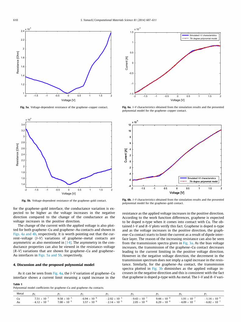
Fig. 5a. Voltage-dependent resistance of the graphene–copper contact.
-2 -1.5 -1 -0.5 0 0.5 1 1.5 2
1.4
1.6
1.8
2
2.2
2.4
2.6
2.8
3
3.2
3.4
x 104
Voltage [V]
Res
ista
nce
[Ohm
]
Fig. 5b. Voltage-dependent resistance of the graphene–gold contact.
-2 -1.5 -1 -0.5 0 0.5 1 1.5 2-1.5
-1
-0.5
0
0.5
1
1.5x 10⁻⁴
Voltage [V]
Cur
rent
[A]
Simulated I-V characteristics 7th degree polynomial model
Fig. 6a. I–V characteristics obtained from the simulation results and the presentedpolynomial model for the graphene–copper contact.
Fig. 6b. I–V characteristics obtained from the simulation results and the presentedpolynomial model for the graphene–gold contact.
610 S. Yamacli / Computational Materials Science 81 (2014) 607–611
for the graphene–gold interface, the conductance variation is ex-pected to be higher as the voltage increases in the negativedirection compared to the change of the conductance as thevoltage increases in the positive direction.
The change of the current with the applied voltage is also plot-ted for both graphene–Cu and graphene–Au contacts and shown inFigs. 4a and 4b, respectively. It is worth pointing out that the cur-rent–voltage (I–V) variations of graphene–metal contacts areasymmetric as also mentioned in [14]. The asymmetry in the con-ductance properties can also be viewed in the resistance–voltage(R–V) variations that are shown for graphene–Cu and graphene–Au interfaces in Figs. 5a and 5b, respectively.
4. Discussion and the proposed polynomial model
As it can be seen from Fig. 4a, the I–V variation of graphene–Cuinterface shows a current limit meaning a rapid increase in the
Table 1Polynomial model coefficients for graphene–Cu and graphene–Au contacts.
Metal p0 p1 p2 p3
Cu 7.51 � 10�7 9.58 � 10�5 �6.94 � 10�6 �2.92 � 10�5
Au �4.12 � 10�7 7.00 � 10�5 3.57 � 10�6 �2.14 � 10�5
resistance as the applied voltage increases in the positive direction.According to the work function differences, graphene is expectedto be doped n-type when it comes into contact with Cu. The ob-tained I–V and R–V plots verify this fact. Graphene is doped n-typeand as the voltage increases in the positive direction, the graph-ene–Cu contact starts to limit the current as a result of dipole inter-face layer. The reason of the increasing resistance can also be seenfrom the transmission spectra given in Fig. 3a. As the bias voltageincreases, the transmission of the graphene–Cu contact decreasesleading to the current limiting in the positive voltage direction.However in the negative voltage direction, the decrement in thetransmission spectrum does not imply a rapid increase in the resis-tance. Similarly, for the graphene–Au contact, the transmissionspectra plotted in Fig. 3b diminishes as the applied voltage in-creases in the negative direction and this is consistent with the factthat graphene is doped p-type with Au metal. The I–V and R–V vari-
p4 p5 p6 p7
�9.43 � 10�7 9.44 � 10�6 1.91 � 10�7 �1.14 � 10�6
2.05 � 10�6 6.29 � 10�6 �4.09 � 10�7 �6.82 � 10�7

S. Yamacli / Computational Materials Science 81 (2014) 607–611 611
ations of Figs. 4b and 5b also show that the current limiting and therapid resistance increment occur in the negative voltage directionfor the graphene–Au contact. It is worth noting that the asymmetryin resistance obtained in this work is in consistency with the the-oretical explanation given in [14] and the experimental results re-ported in [15]. Moreover, the asymmetric resistance–voltagedependency of the p-type graphene–metal contact shown inFig. 5b is in consistency with the experimentally measured charac-teristics given in [28]. This also verifies the results of our study.
The behaviour of graphene–metal contact depends on the workfunction differences [13] and the interface length [16] hence simi-lar I–V and R–V characteristics can obviously be observed for othertypes and interface lengths of graphene–metal contacts. Consider-ing the obtained I–V and R–V characteristics, it is shown that a 7thorder polynomial model, which can be used in nanoscale circuitdesign tools, accurately represents electrical characteristics ofgraphene–metal contacts. Presented model is given in Eq. (1).The polynomial model fits to both n-type and p-type graphene–metal contacts only by adjusting the coefficients which are calcu-lated in MATLAB environment. Obtained model parameters are gi-ven in Table 1 for both graphene–Cu and graphene–Au contacts.
IðVÞ ¼X7
i¼0
piVi ð1Þ
In respectively Figs. 6a and 6b, the I–V behaviours of n-type andp-type graphene–metal contacts obtained by the self-consistentsimulations and the proposed polynomial model are shown onthe same axes. As it can be seen from these figures, the presentedmodel accurately represents I–V behaviours of graphene–metalcontacts. Note that the presented model can be used for othergraphene–metal contacts with different metal types and variouscontact lengths only by recalculating the model parametersaccording their I–V characteristics obtained from simulations.
5. Conclusions
Electronic transport properties of p-type and n-type graphene–metal contacts are investigated from nanoelectronics point of viewin this study. The variation of the transmission spectra of graphene–Cu and graphene–Au interfaces are obtained using self-consistentquantum mechanical simulations for the applied voltage range of(�2 V, 2 V). It is observed that the change of the transmission spec-trum of n-type graphene–Cu contact is negligible when the voltageis increased in the negative voltage direction but decreases consid-erably in the positive increasing applied voltage. This situation isthe opposite for the graphene–Au contact as expected. These resultsverify that graphene is n-type and p-type doped with Cu and Aucontact metals, respectively. The current–voltage variations of thecontacts are also obtained and then the voltage-dependent resis-tances are calculated for the first time in the literature. Finally, itis shown that a 7th order polynomial model that is useful for nano-scale design process accurately represents I–V variation of graph-ene–metal contacts, which is another novelty of this work.
Acknowledgement
The author would like to thank Quantumwise A.S. and Dr. An-ders Blom for their valuable support.
References
[1] A.K. Geim, K.S. Novoselov, Nature Materials 6 (2007) 183–191.[2] A.A. Balandin, S. Ghosh, W. Bao, I. Calizo, D. Teweldebrhan, F. Miao, C.N. Lau,
Nano Letters 8 (3) (2008) 902–907.[3] J.U. Lee, D. Yoon, H. Cheong, Nano Letters 12 (9) (2012) 4444–4448.
[4] M.F. Al-Kady, V. Strong, S. Dubin, R.B. Kaner, Science 35 (6074) (2012) 1326–1330.
[5] M. Sprinkle, D. Siegel, Y. Hu, J. Hicks, A. Tejeda, A. Taleb-Ibrahimi, P. Le Fevre, F.Bertran, S. Vizzini, H. Enriques, S. Chiang, P. Soukiassan, C. Berger, W.A. deHeer, A. Lanzara, E.H. Conrad, Physical Review Letters 103 (226803) (2009).
[6] K. Nagashio, T. Nishimura, A. Toriumi, Applied Physics Letters 102 (2013)173507.
[7] E.H. Hwang, S. Adam, S. Des Sarma, Physical Review Letters 98 (18) (2007)186806.
[8] S. Datta, Quantum Transport: Atom to Transistor, Cambridge University Press,UK, 2005.
[9] C. Xu, H. Li, K. Banerjee, IEEE Transactions on Electron Devices 56 (8) (2009)1567–1678.
[10] H. Liu, B. Chen, X. Li, C. Lu, Y. Ding, B. Lu, Physics Procedia 32 (2012) 228–234.[11] M.J. Allen, V.C. Tung, R.B. Kaner, Chemical Review 110 (1) (2010) 132–145.[12] B.J. Schultz, C. Jaye, P.S. Lysaght, D.A. Fischer, D. Prendergast, S. Banerjee,
Chemical Science 4 (2013) 494–502.[13] F. Schwierz, Nature Nanotechnology 5 (2010) 487–496.[14] P.A. Khomyakov, G. Giovanetti, P.C. Rusu, G. Brocks, J. van den Brink, P.J. Kelly,
Physical Review B 79 (19) (2009) 195425.[15] W. Liu, J. Wei, X. Sun, H. Yu, Crystals 3 (2013) 257–274.[16] B. Huard, N. Stander, J.A. Sulpizio, D. Goldhaber-Gordon, Physical Review B 78
(2008) 121402.[17] K. Nagashio, T. Nishimura, K. Kita, A. Toriumi, IEEE International Electron
Devices Meeting (2009) 1–4.[18] A. Toriumi, K. Nagashio, T. Moriyama, R. Ifuku, ECS Transactions 53 (1) (2013)
71–79.[19] K. Stokbro, M. Engelund, A. Blom, Physical Review B 85 (2012) 165442.[20] S. Barraza-Lopez, M. Vanevic, M. Kindermann, M.Y. Chou, Physical Review
Letters 104 (2010) 076807.[21] F. Xia, V. Perebinos, Y.-M. Lin, Y. Wu, Ph. Avouris, Nature Nanotechnology 6
(2011) 179–184.[22] H.B. Heersche, P. Jarillo-Herrero, J.B. Oostinga, L.M.K. Vandersypen, A.F.
Norpoutgo, Nature 446 (2007) 56–59.[23] X. Du, I. Skachko, A. Barker, E.Y. Andrei, Nature Nanotechnology 3 (2008) 491–
495.[24] R. Danneau, F. Wu, M.F. Cracium, S. Russo, M.Y. Tomi, J. Salmilehto, A.F.
Morpurgo, P.J. Hakonen, Physical Review Letters 100 (19) (2008) 196802.[25] E.J.H. Lee, K. Balasubramanian, R.T. Wietz, M. Burghard, K. Kern, Nature
Nanotechnology 3 (2008) 486–491.[26] S. Russo, M. Craciun, M. Yamamoto, A. Morpurgo, S. Tarucha, Physica E 42
(2010) 677–679.[27] J.A. Robinson, M. LaBella, M. Zhu, M. Hollander, R. Kasarda, Z. Hughes, K.
Trumbull, R. Cavalero, D. Snyder, Applied Physics Letters 98 (2011) 053103.[28] L. Jiao, X. Wang, G. Diankov, H. Wang, H. Dai, Nature Nanotechnology 5 (2010)
321–325.[29] K.S. Novoselov, A.K. Geim, S.V. Morozov, D. Jiang, Y. Zhang, S.V. Dubonos, I.V.
Grigorieva, A.A. Firsov, Science 306 (5696) (2004) 666–669.[30] Y. Zhang, Y.-W. Tan, H.L. Stormer, P. Kim, Nature 438 (2005) 201–204.[31] M.Y. Han, B. Ozyilmaz, Y. Zhang, P. Kim, Physical Review Letters 98 (2007)
206805.[32] P. Blake, R. Yang, S.V. Morozov, F. Schedin, L.A. Ponomarenko, A.A. Zhukov, R.R.
Nair, I.V. Grigorieva, K.S. Novoselov, A.K. Geim, Solid State Communications149 (27–28) (2009) 1068–1071.
[33] C. Malec, D. Davidovic, Physical Review B 84 (2011) 033407.[34] C. Malec, D. Davidovic, Journal of Applied Physics 109 (2011) 064507.[35] C. Malec, B. Elkus, D. Davidovic, Solid State Communications 151 (23) (2011)
1791–1794.[36] J. Knoch, Z. Chen, J. Appenzeller, IEEE Transactions on Nanotechnology 11 (3)
(2012) 513–519.[37] H. Liu, H. Kondo, T. Ohno, Physical Review B 86 (2012) 155434.[38] V. Nam Do, H. Anh Le, Applied Physics Letters 101 (2012) 161605.[39] Y. Takagi, S. Okada, Japanese Journal of Applied Physics 51 (8) (2012) 085102.[40] S. Barraza-Lopez, M. Kindermann, M.Y. Chou, Nano Letters 12 (7) (2012) 3424–
3430.[41] S. Barraza-Lopez, Journal of Computational Electronics 12 (2) (2013) 145–164.[42] V. Nam Do, P. Dollfus, Journal of Physics: Condensed Matter 22 (2010) 425301.[43] J. Maassen, W. Ji, H. Guo, Applied Physics Letters 97 (14) (2010) 142105.[44] W.M. Haynes (Ed.), Handbook of Chemistry and Physics, 94th ed., CRC Press,
USA, 2013.[45] L. Leem, A. Srivastava, S. Li, B. Magyari-Köpe, G. Iannacone, J. Harris, G. Fiori,
IEEE Electron Devices Meeting (2010) 32.5.1–32.5.4.[46] N. Lebedev, I. Griva, A. Blom, Journal of Physical Chemistry 117 (14) (2013)
6933–6939.[47] S. Barzilai, F. Tavvazza, L.E. Levine, Modelling and Simulation in Materials
Science and Engineering 21 (2) (2013) 025004.[48] S. Chauhan, P. Srivastava, A.K. Shrivastava, Journal of Computational and
Theoretical Nanoscience 9 (12) (2012) 2215–2216.[49] Atomistix Toolkit (ATK) Manual, Quantumwise AS, Denmark, 2013.[50] G.B. Abadir, K. Walus, D.L. Pulfrey, Journal of Computational Electronics 8
(2009) 1–9.[51] The International Technology Roadmap for Semiconductors (ITRS),
www.itrs.net, 2013.