Embed Size (px)
Citation preview

This journal is © the Owner Societies 2021 Phys. Chem. Chem. Phys., 2021, 23, 24699–24710 | 24699
Cite this: Phys. Chem. Chem. Phys.,
2021, 23, 24699
First principles simulations of microscopicmechanisms responsible for the drastic reductionof electrical deactivation defects in Sehyperdoped silicon
Alberto Debernardi
By first principles simulations we systematically investigate Se hyperdoped silicon by computing, for
different types of Se complexes, the formation energy as a function of dopant concentration. We
identify the microscopic mechanisms responsible for the dramatic reduction of electrical deactivation
defects as the dopant concentration approaches the critical value, xc, at which the insulator-to-metal
transition occurs. We discuss the electrical properties of Se point defects and Se complexes, shedding
light on the formation and the nature of the impurity band in the bandgap and how the presence of
different types of complexes may increase the broadening of the impurity band and affects the
insulator-to-metal transition. We identify the best doping range in which the properties of the impurity
band can be engineered according to the needs of the electronic industry. Simulations of the structural
properties of the complexes complete the work. Our findings are relevant for intermediate impurity
band applications.
I Introduction
Silicon hyperdoped (i.e., doped beyond the solid solubilitylimit) with donor impurities is attracting increasing attentionfrom the electronic industry and materials science communitybecause it is a promising candidate as a building block for theconception of new electronic devices ranging from infraredabsorbers,1–3 to intermediate band photovoltaics4,5 to ultra-scaled nano-electronics6. The latter application is motivatedby the continuous scaling down of Si-based transistors in on-chip complementary metal oxide semiconductor (CMOS)devices, which are approaching the 2 nm technology node.Therefore, the next generation of ultra-scaled CMOS devicesrequires extremely high free-electron densities, of the order of1021 cm�3 (i.e. one electron per nm3) to ensure sufficient freecarriers in a transistor to work.7,8
Shallow donors, such as group V elements (P, As, or Sb),are traditionally employed as dopants in Si for their low ioniza-tion energy, low diffusivity and suitable solid solubility. Unfortu-nately, their free-electron concentration saturates at around5 � 1020 cm�3:9,10 beyond this concentration the introductionof further donors does not generate free carriers, thus providingan upper limit for the electron density, preventing the realizationof nanometer-size devices.
In the last few decades, experimental11–13 and theoretical14–16
works studied the microscopic mechanisms responsible forsaturation of free-electron concentration in group V dopants inSi. The saturation has been attributed to the formation ofelectrical deactivation defects. According to the literature, thesedefects have been identified with different types of substitutioncomplexes: the Asn–VSi (n r 4) model (the clustering around a Sivacancy, VSi, surrounded by As atoms,12,14–23 also invoked tointerpret Sbn–VSi clusters24); the dimers (substitutional dopant innearest neighbor (NN) lattice sites)25 and the defects containingpairs of separated dopant atoms (in next NN lattice sites) withoutvacancies.25,26 These group V complexes introduce deep acceptorstates in the bandgap that deactivate free carriers, thus preventinghigh electron concentrations.25,26
At variance, chalcogen impurities (group VI elements: S, Se, andTe) are deep donors in Si, having ionization energy of a few hundredsof meV at low concentration, while at high concentration they caninduce free electrons (in excess of 1020 cm�3) in Si, accompanied byan insulator-to-metal transition (IMT).27,28 Chalcogens show superiorelectronic properties as Si hyper-dopants than traditional group Velements: a Te concentration of 1.25 � 1021 cm�3 has been reachedin hyperdoped Si without showing any sign of saturation,6,29 whilethe electron concentration (8.1 � 1020 cm�3 6) in the same samplesnearly scored the target of 1021 cm�3 required for the next generationof the Si technology node.7,9,30
Furthermore, hyper-doping establishes a new materialsplayground to investigate impurity mediated IMTs in
CNR-IMM, Unit of Agrate Brianza, via C. Olivetti 2, 20864 Agrate Brianza (MB),
Italy. E-mail: [email protected]
Received 26th June 2021,Accepted 8th October 2021
DOI: 10.1039/d1cp02899e
rsc.li/pccp
PCCP
PAPER
Ope
n A
cces
s A
rtic
le. P
ublis
hed
on 0
8 O
ctob
er 2
021.
Dow
nloa
ded
on 4
/9/2
022
4:49
:37
AM
. T
his
artic
le is
lice
nsed
und
er a
Cre
ativ
e C
omm
ons
Attr
ibut
ion-
Non
Com
mer
cial
3.0
Unp
orte
d L
icen
ce.
View Article OnlineView Journal | View Issue

24700 | Phys. Chem. Chem. Phys., 2021, 23, 24699–24710 This journal is © the Owner Societies 2021
semiconductors, that has been largely studied both for itsinterest in fundamental physics and for its relevance intechnological applications. Previous studies about IMT inS27,31 and Se28 hyperdoped Si have been focused on the singlesubstitutional impurities, while recently, first principles simu-lations have enlightened the role of dimers as a driving force ofIMT in Te hyperdoped Si.6,29
Computational studies are therefore desirable to validatethis scenario, by considering other chalcogen dopants, andadditional types of chalcogen complexes, to provide novelinsights into the microscopic mechanisms governing the hyper-doped regime in Si.
In this work we present first principles simulations of theformation energy of different complexes in Se hyperdoped Si ina wide range of dopant concentrations.
This article is structured as follows: in Section II we describethe computational techniques used in the work; in Section III.A wedisplay our results for the formation energy of the different types ofdefects investigated as a function of dopant concentration; for eachdefect, we present our first principles results for the electronic, andthe structural properties, respectively in Sections III.B and III.C.In Section IV we discuss our finding in relation to applications inwhich Se hyperdoped silicon can be used as building block ininnovative devices based on the formation of an intermediateimpurity band in the electronic gap. Finally, in Section V we presentour conclusions and summarize our results.
II Computational methods
In our simulations we consider Se interstitial ISe, single Sesubstitutional, SeSi, Se dimers SeSi–SeSi and complexes formedby a Si vacancy VSi surrounded by m Se atoms, denoted as(SeSi)m–VSi, m = 1, 2, 3, 4. Although the latter complexes havebeen extensively studied for group V donors (mainly As), thepossible role of the clustering of chalcogen atoms arounda vacancy seems still unexplored by ab initio simulations.Geometrical models of neutral single vacancy-seleniumcomplexes are determined from first principles by plane-wavepseudopotentials techniques. We will present the formationenergy of these complexes as a function of the Se concentration,and we will discuss electrical properties to enlighten theadvantages of chalcogen atoms as dopants in forthcomingnanometer-size devices based on hyperdoped Si.
Our simulations are obtained using the super-cell methodwithin the single complex model (SCM); accuracy and limit ofSCM, and all computational details are discussed inAppendix A.
III ResultsA Defect formation energy
We denote with D a generic defect among the ones consideredin the present work (i.e. D A ISe, SeSi, SeSi–SeSi and (SeSi)m–VSi,m = 1, 2, 3, and 4). For the defect D, the formation energy per Se
atom as a function of Se concentration x, in hyperdoped silicon(Si1�xSex), reads
DEFormD (x) � [ED(x) � NSimSi � NSemSe]/NSe (1)
where ED(x) is the total energy of the supercell with D (a pointdefect or a complex), NSi and NSe are the numbers of Si and Seatoms in the supercell, respectively, and mSi and mSe correspond tothe chemical potentials of bulk Si and bulk SiSe2 at equilibriumwith each other.
In Fig. 1 and 2 we display our computed formation energy atdifferent doping concentrations for all complexes investigated.Note that, accordingly to the choice of the chemical potentials,the zero of the energy corresponds to the phase separation ofSi1�xSex into bulk Si and SiSe2, and all Se complexes presentpositive formation energy, in agreement with the experimentalfact that, in the concentration range considered, Si is dopedbeyond the Se solid solubility limit.6,32
By the comparison of the energy scales of the two figureswe can immediately appreciate that at high concentration(x \ 0.45 at%) the formation energies of the complexesdisplayed in Fig. 2 (ISe and SeSi–VSi) are more than one eVhigher that the ones of Fig. 1, thus making unlikely, at least athigh concentration, the formation of the complexes displayedin Fig. 2, as discussed below.
For convenience, in the following discussion, we distinguish,for each type of defect D, three different ranges of doping: (1) thehighly diluted range (x { 1), in which the average distancebetween different complexes is so high that the complexes canbe considered as non-interacting; (2) the interaction range, inwhich the average distances between randomly distributedcomplexes allow a non-negligible overlap of the wave-functionof different complexes, producing a impurity band (IB) in thegap; and (3) the fully metallic range for concentration greaterthan the concentration xM(D) at which the IB merges into the
Fig. 1 Formation energy (per atom) of Se substitutional impurities andtheir complexes with a silicon vacancy. Solid lines are a guide for the eye.
Paper PCCP
Ope
n A
cces
s A
rtic
le. P
ublis
hed
on 0
8 O
ctob
er 2
021.
Dow
nloa
ded
on 4
/9/2
022
4:49
:37
AM
. T
his
artic
le is
lice
nsed
und
er a
Cre
ativ
e C
omm
ons
Attr
ibut
ion-
Non
Com
mer
cial
3.0
Unp
orte
d L
icen
ce.
View Article Online

This journal is © the Owner Societies 2021 Phys. Chem. Chem. Phys., 2021, 23, 24699–24710 | 24701
conduction band; in this range the electrons originating from theIB are de-localized in the conduction bands thus contributing tothe metallic behaviors.
The ab initio simulation of a highly diluted range, requiringenormous size super-cells, is beyond the scope of the presentwork, which is focused on the interaction and the metallicranges corresponding to hyper-doping. Donor complexes inhighly diluted range have localized wave-functions, producingenergy levels in the bandgap having sharp (zero or negligible)linewidth due to negligible overlap between the wave-functionsof different defects. In this range the formation energy isalmost equal to the one of the isolated defect, DEForm
D (0).As the concentration increases (interaction range), the inter-
action between neighboring complexes produces an IB whosewidth increases for increasing overlap, and the formationenergy steeply increases up to the concentration at which thesystem presents metallic states delocalized in the whole crystal.
In the fully metallic range, for x 4 xM, the IB is mergedinto the conduction band providing conduction electrons andeventually contributing to a metallic screening of the impuritycomplex, and DEForm
D (x) is a smooth function of x.As it will be illustrated in the next section, the different types
of complexes, can be divided in two sets: complexes that in theinteraction range have an insulating IB, denoted as Dins andcomplexes that in the interaction range have a metallic IB,denoted as Dmet. For the latter complexes, we define xs(Dmet) asthe concentration at which DEForm
D (x) becomes smooth; ingeneral, xs(Dmet) t xM(Dmet), the non-equality holds probablyas a consequence of the screening effects due to the formationof a metallic band.
In general, for all type of complexes investigated, the formationenergy increases monotonically with increasing concentration;DEForm
D (x) is steep in the interaction range (up to xs for Dmet),while it is rather flat in the metallic range. The decrease of
DEFormSeSi (x) for x 4 3 at% is probably due to the mutual interaction
of different SeSi, that above the xM(SeSi) produces a lowering of theformation energy approaching the one of dimers as the concen-tration increases.
These differences in DEFormD (x) explain the prevalence of
complexes involving substitutional Se with respect to Se inter-stitials in the metallic range, detected in experimental studies,since according to our simulations the former complexes havelower formation energy in the region where DEForm
D (x) is flat.Although similar differences in DEForm
D (x) can be also noticed inthe lower values of x range considered, a local fluctuation of theconcentration Dx, provided by the random distribution ofdopants, can cause a significant variation in the formationenergy of the complex if x is within the interaction range inwhich DEForm
D (x) is steep, thus preventing the complexes havingthe lowest DEForm
D (x) to become the dominant ones.To better illustrate this concept, we consider two complexes D1
and D2 for which DEFormD1
xð ÞoDEFormD2
xð Þ; if x is within the steep
range of DEFormD (x) and a local increase (decrease) Dx1 (�Dx2) occurs
in a region of the crystal where the complexes D1 (D2) are present,this fluctuation can produce DEForm
D1ðxþ Dx1Þ4DEForm
D2ðx� Dx2Þ.
At variance, if x is within the metallic range, where DEFormD (x)
is smooth, the formation energy is only slightly affected by alocal fluctuation of x (in fact, in the smooth range a localfluctuation does not change the inequality DEForm
D1ðxþ Dx1Þo
DEFormD2ðx� Dx2Þ), and thus the complexes having lowest
DEFormD (x) are the predominant ones that we expect to detect
in an experiment.The complexes formed by one substitutional Se nearest-
neighbour (NN) to a Si vacancy, SeSi–VSi, and the Se interstitial,ISe, in the hexagonal or in the tetrahedral position, havesignificantly higher formation energy than the other complexesinvestigated; for x \ 0.45 at% the formation energy of thesecomplexes is smooth, and consequently, the formation of thesecomplexes is unlikely, explaining the dramatic reduction ofinterstitial Se at these concentrations as experimentallydetected in Se hyperdoped Si.32,33 A similar mechanism hasbeen also found in Te hyperdoped Si6 (by comparing DEForm
D ofITe, TeSi, TeSi–TeSi).
B Electronic bandstructure
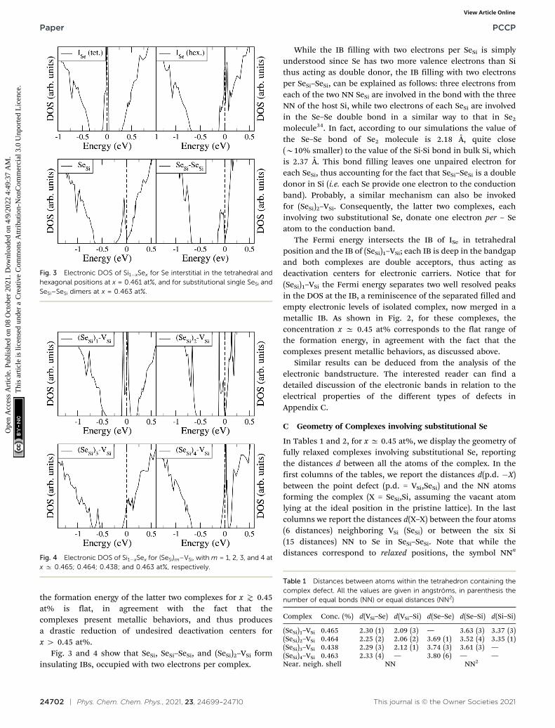
To analyze the electronic properties of different defects, inFig. 3 and 4 we display the Density of States (DOS) of thedifferent types of complexes studied for x A [0.44–0.46] at%.With this choice of x, all types of defects considered have equalor very similar Se concentration thus allowing the comparisonbetween the IB of different complexes.
At this concentration, the IB of ISe in the hexagonal positionand the IB of (SeSi)3–VSi have already been merged with theconduction band, while the IBs formed by the other complexesare within the bandgap originated from the Si gap. (SeSi)4–VSi
has a shallow metallic IB. At variance, ISe in the tetrahedralposition and (SeSi)1–VSi have metallic IB deep in the bandgap,and both complexes are double acceptors, thus acting asdeactivation centers for electronic carriers. According to Fig. 2
Fig. 2 Formation energy (per atom) of Se interstitials and the complexformed by Se substitutional with a silicon vacancy.
PCCP Paper
Ope
n A
cces
s A
rtic
le. P
ublis
hed
on 0
8 O
ctob
er 2
021.
Dow
nloa
ded
on 4
/9/2
022
4:49
:37
AM
. T
his
artic
le is
lice
nsed
und
er a
Cre
ativ
e C
omm
ons
Attr
ibut
ion-
Non
Com
mer
cial
3.0
Unp
orte
d L
icen
ce.
View Article Online
24702 | Phys. Chem. Chem. Phys., 2021, 23, 24699–24710 This journal is © the Owner Societies 2021
the formation energy of the latter two complexes for x \ 0.45at% is flat, in agreement with the fact that thecomplexes present metallic behaviors, and thus producesa drastic reduction of undesired deactivation centers forx 4 0.45 at%.
Fig. 3 and 4 show that SeSi, SeSi–SeSi, and (SeSi)2–VSi forminsulating IBs, occupied with two electrons per complex.
While the IB filling with two electrons per SeSi is simplyunderstood since Se has two more valence electrons than Sithus acting as double donor, the IB filling with two electronsper SeSi–SeSi, can be explained as follows: three electrons fromeach of the two NN SeSi are involved in the bond with the threeNN of the host Si, while two electrons of each SeSi are involvedin the Se–Se double bond in a similar way to that in Se2
molecule34. In fact, according to our simulations the value ofthe Se–Se bond of Se2 molecule is 2.18 Å, quite close(B10% smaller) to the value of the Si-Si bond in bulk Si, whichis 2.37 Å. This bond filling leaves one unpaired electron foreach SeSi, thus accounting for the fact that SeSi–SeSi is a doubledonor in Si (i.e. each Se provide one electron to the conductionband). Probably, a similar mechanism can also be invokedfor (SeSi)2–VSi. Consequently, the latter two complexes, eachinvolving two substitutional Se, donate one electron per – Seatom to the conduction band.
The Fermi energy intersects the IB of ISe in tetrahedralposition and the IB of (SeSi)1–VSi; each IB is deep in the bandgapand both complexes are double acceptors, thus acting asdeactivation centers for electronic carriers. Notice that for(SeSi)1–VSi the Fermi energy separates two well resolved peaksin the DOS at the IB, a reminiscence of the separated filled andempty electronic levels of isolated complex, now merged in ametallic IB. As shown in Fig. 2, for these complexes, theconcentration x C 0.45 at% corresponds to the flat range ofthe formation energy, in agreement with the fact that thecomplexes present metallic behaviors, as discussed above.
Similar results can be deduced from the analysis of theelectronic bandstructure. The interested reader can find adetailed discussion of the electronic bands in relation to theelectrical properties of the different types of defects inAppendix C.
C Geometry of Complexes involving substitutional Se
In Tables 1 and 2, for x C 0.45 at%, we display the geometry offully relaxed complexes involving substitutional Se, reportingthe distances d between all the atoms of the complex. In thefirst columns of the tables, we report the distances d(p.d. �X)between the point defect (p.d. = VSi,SeSi) and the NN atomsforming the complex (X = SeSi,Si, assuming the vacant atomlying at the ideal position in the pristine lattice). In the lastcolumns we report the distances d(X–X) between the four atoms(6 distances) neighboring VSi (SeSi) or between the six Si(15 distances) NN to Se in SeSi–SeSi. Note that while thedistances correspond to relaxed positions, the symbol NNn
Fig. 3 Electronic DOS of Si1�xSex for Se interstitial in the tetrahedral andhexagonal positions at x = 0.461 at%, and for substitutional single SeSi andSeSi–SeSi dimers at x = 0.463 at%.
Fig. 4 Electronic DOS of Si1�xSex for (SeSi)m–VSi, with m = 1, 2, 3, and 4 atx C 0.465; 0.464; 0.438; and 0.463 at%, respectively.
Table 1 Distances between atoms within the tetrahedron containing thecomplex defect. All the values are given in angstroms, in parenthesis thenumber of equal bonds (NN) or equal distances (NN2)
Complex Conc. (%) d(VSi–Se) d(VSi–Si) d(Se–Se) d(Se–Si) d(Si–Si)
(SeSi)1–VSi 0.465 2.30 (1) 2.09 (3) — 3.63 (3) 3.37 (3)(SeSi)2–VSi 0.464 2.25 (2) 2.06 (2) 3.69 (1) 3.52 (4) 3.35 (1)(SeSi)3–VSi 0.438 2.29 (3) 2.12 (1) 3.74 (3) 3.61 (3) —(SeSi)4–VSi 0.463 2.33 (4) — 3.80 (6) — —Near. neigh. shell NN NN2
Paper PCCP
Ope
n A
cces
s A
rtic
le. P
ublis
hed
on 0
8 O
ctob
er 2
021.
Dow
nloa
ded
on 4
/9/2
022
4:49
:37
AM
. T
his
artic
le is
lice
nsed
und
er a
Cre
ativ
e C
omm
ons
Attr
ibut
ion-
Non
Com
mer
cial
3.0
Unp
orte
d L
icen
ce.
View Article Online

This journal is © the Owner Societies 2021 Phys. Chem. Chem. Phys., 2021, 23, 24699–24710 | 24703
labels the atoms according to the ideal positions in the pristinelattice in the n-th NN shell from the p.d. The (SeSi)m–VSi
complexes show an inward relaxation of Se toward the vacancy.At variance, for SeSi the relaxed d(Se–Si) is 8% isotropicallylarger than the simulated ideal Si–Si bond (2.37 Å).
Since they can be measured by Rutherford back-scatteringspectrometry in channeling geometry (RBS-C), we report, forx C 0.45 at%, the atomic displacements of Se from the idealposition in the pristine lattice. While for (SeSi)m–VSi, m = 1, 3, or4, the atomic displacement is very small (about 0.06, 0.08, and0.04 Å for m = 1, 3, and 4, respectively) for SeSi–SeSi and (SeSi)2–VSi the Se displacement is 0.39 Å, and 0.12 Å, respectively,representing a fingerprint of the peculiar bond formedby couples of chalcogen donors in Si. Similar values of Sedisplacements are obtained for other concentrations.
IV Discussion
We briefly discuss our finding in view of possible applicationsof chalcogen hyperdoped Si as the building block in broadband infra-red detectors or intermediate band photo-voltaics.Both applications are based on the formation of a relativelyshallow IB.
At room temperature – the usual device working temperature –all IB electrons are thermally excited in the conduction band,while the absorption of infra-red radiation (or of sunlight tophoto-generate electric current for photo-voltaics) is producedby the excitation of valence-band electrons into the IB.
Our goal is to determine the best doping range for theseapplications.
Assuming a uniform random distribution of substitutionalSe in the lattice sites, the complexes involving three or moredonors are extremely unlikely (for a quantitative analysis seeAppendix B). The complexes of Fig. 1 involving up to two Sehave insulating IB, for these Dins defects we found
0.46 at% D xM(SeSi) o xM((SeSi)2–VSi) o xM(SeSi–SeSi)
D 0.93 at% (2)
A first technological requirement is to maximize the electronsin conduction band by drastically reducing the electricaldeactivation complexes.
According to the above analysis for x \ 0.46 at% the systempresents a dramatic reduction of the deactivation complexes ISe
and (SeSi)1–VSi.
Notice that, for x \ 0.46 at%, the other types of complexeshaving a metallic IB don’t act as acceptors, because they have(1) a shallow IB, which is fully ionized at room temperature(as (SeSi)4–VSi at x = 0.46 at%); or they have (2) the IB mergedinto the conduction band (xM((SeSi)3–VSi) o 0.43 at%).
This condition determines the lower limit of the best dopingrange, xinf = xM(SiSe).
A second technological requirement is the presence of abroad IB in the gap. As shown in Fig. 3 and 4 different types ofcomplexes have different IB-widths and different IB-centers,their DOS overlap only partially in the energy interval corres-ponding to the IBs; these overlap of the DOS contributes tofurther increase the total width of the resulting IB (which is thesum of the IB of all types of defects present in the sample), atleast up to the concentration xM(SeSi–SeSi) that correspondsto the greater xM among the donor complexes that have non-negligible probability to be present in the sample.
The highest xM dictates the upper limit of the best concen-tration range since it determines the extinction of the IB due tothe merging into the conduction band. So, we chose xsup �xM(SeSi–SeSi) C 0.93 at%, since for x 4 xsup we expect that IB ofthe large majority of Se complexes are merged into theconduction band.
Thus, we suggest that the optimal doping values for inter-mediate IB application ranges between xinf (C0.46 at%), andxsup (C0.93 at%); in this range in which a shallow IB is presentand is providing the maximum carrier density per donor sincethe electrical deactivating defects are drastically reduced.
The variation of the dopant concentration within theoptimal range provides a tunable mechanism to modify theIB minimum, according to the needs of the electronic industry.
Finally, some considerations about the estimation of xc
within SCM. Neglecting for simplicity Dmet complexes, if onlyone type of defect D is present, the critical temperaturecorresponds to xM(D). If more than one type of complex ispresent, what is the critical concentration xc at which the IMToccurs? By using a simple model in which the complex wave-function is localized around the impurity and the IB is formedby a tight-binding like form, we propose the formula to evaluatexc from the values xM obtained by first principles:
1
xc¼Xn
cn
xMðDnÞ; (3)
where cn is the number of Se forming complexes of type Dn
divided by the total number of Se. Clearly,Pn
cn ¼ 1 and n
ranges over all different types of complexes.A simple estimation of most probable defects (assuming a
limited mobility of random distributed Se combined withthermal weights, see also Appendix B) gives xc = 0.50 at%.The xc value is mainly determined by xM of the SeSi population(xM C 0.46, cn B 84%) with respect to the SeSi–SeSi one (xM C0.93, cn B 16%). Our results suggest that the presence ofdifferent complexes may increase the IB broadeningthus affecting the conductivity of the system, the xc, and thesharpness of the IMT as a function of x.
Table 2 Distances between atoms within the tetrahedron (two tetrahe-dra) containing the SeSi (SeSi–SeSi) defect (complex). All the values aregiven in angstroms, in parenthesis the number of equal bonds (NN) orequal distances (NNn, n Z 2)
ComplexConc.(%) d(Se–Se) d(Se–Si) d(Si–Si)
SeSi 0.463 — 2.57 (4) 4.19 (12) — — —SeSi–SeSi 0.463 3.15 (1) 2.44 (3) 4.37 (3) 4.12 (6) 4.82 (6) 6.34 (3)Near. neigh. shell NN NN2 NN3 NN4
PCCP Paper
Ope
n A
cces
s A
rtic
le. P
ublis
hed
on 0
8 O
ctob
er 2
021.
Dow
nloa
ded
on 4
/9/2
022
4:49
:37
AM
. T
his
artic
le is
lice
nsed
und
er a
Cre
ativ
e C
omm
ons
Attr
ibut
ion-
Non
Com
mer
cial
3.0
Unp
orte
d L
icen
ce.
View Article Online

24704 | Phys. Chem. Chem. Phys., 2021, 23, 24699–24710 This journal is © the Owner Societies 2021
V Conclusions
In summary, by first principles simulations, we enlighten themicroscopic mechanisms responsible for the removal ofelectrical deactivation defects in Se hyperdoped Si. We studiedthe formation energy as a function of the dopant concentrationand the electronic and structural properties of different Secomplexes to identify the optimal doping range, in which thedonor density can be tuned to engineering the width andthe shallowness of the IB for intermediate IB applications.Our findings can be extended to silicon hyperdoped with otherchalcogen impurities, paving the way toward an intermediateIB electronics of nanometer size.
Conflicts of interest
There are no conflicts to declare.
AppendixAppendix A: Computational details
We performed our first principles calculations of structuraland electronic properties of Se hyperdoped silicon within theframework of Density Functional Theory (DFT) by solving theKohn–Sham equations through the plane-wave pseudopotentialapproach as implemented in QUANTUM ESPRESSO (QE) open-source package35. In our simulations we used ultra-softpseudopotentials36,37 in the separable form introduced byKleinmann and Bylander38, generated using a Perdew–Burke–Ernzerhof (PBE)39 exchange correlation functional. For metallicsystems, i.e. for defects having a metallic IB or for defects havingan insulating IB at concentration above the Insulator to MetalTransition (IMT) threshold (x 4 xM), we used smearingtechniques with a Gaussian broadening of 1 mRy. We choose a40-Ry cutoff radius for the electronic valence wave function and400-Ry cutoff radius for the charge density. The computed latticeparameter of bulk Si is aL = 5.475 Å (while aL = 5.431 Å is theexperimental value, from ref. 40).
To simulate the hyperdoped silicon we used the super-cell(SC) method, consisting in the use of large simulation cellscontaining Se defects. We fully exploit the cubic symmetry ofthe silicon lattice by building super-cells with different cubicsymmetry to increase for each type of defect the set of differentdoping concentration considered, maintaining the super-cellswithin a size that can be computationally affordable by our firstprinciples techniques. For this purpose, by using periodic (i.e.,Born–von Karman) boundary conditions, we consideredsimulation cells of different sizes, each containing a differenttype of Se point defect or Se complex as detailed in the following.
Bulk silicon presents the diamond structure constituted by aface center cubic (fcc) lattice plus a two atom basis. The fccprimitive lattice vectors -afcc
i (I = 1, 2, or 3), can be repeatedM-times, with M a positive integer, to form super-cell of fccsymmetry, denoted fcc-MMM, composed of M3 unit cells.Explicitly, the super-cell lattice vectors are -
asci � M
-afcc
i (i = 1,2, 3), where the same integer M is multiplied by each primitive
lattice vector to ensure uniform and isotropic dopant distribution,when the super-cell contain one point defect or a isotropiccomplex as (SeSi)4–VSi, while it is true with a good approximationif the defect is non-isotropic. Since the unit cell contains 2 atoms,the repetition of the unit cell according a fcc lattice providessuper-cells having size 2MMM (i.e. 16, 54, 128, 250, 432, 686,. . .,for M = 2, 3, 4, 5, 6, 7,. . .). Since different types of cubicsymmetries are possible, a different choice of cubic symmetryprovides different super-cell sizes. The conventional unit cell ofSi is a face centered cube with 8 atoms; we considered theconventional cell, as the unit cell of a simple cubic (sc) lattice(whose primitive lattice vectors coincide with the three orthogonalside of the conventional cube), whose 8 atoms unit-cell can beused to build super-cell of type sc-MMM, having size 8MMM(i.e., 64, 216, 512, 1000, . . ., for M = 2, 3, 4, 5,. . .), in an analogousway as done for the fcc lattice (by replacing fcc label with sc in thedefinition of -
aSCi ). In a similar way, a sc–(2M)(2M)(2M) super-cell
can be seen as body centered cubic (bcc) super-cell containing8ð2MÞ3
2¼ 32�M3 atoms (i.e. 32, 256, 864,. . . for M = 1, 2, 3,. . .).
The use of All Compatible Symmetries (ACS), in the procedure tobuild the super-cell (in the present case we use All types of CubicSymmetries) allows to arrange the doping complexes in a periodicrepeated lattice of cubic symmetry (sc, fcc or bcc). This tricksignificantly increases the number of supercells of different sizes,and is particularly useful, as in our case, in first principlesimulations in which one should limit the computational effortto super-cells having less than one thousand atoms, to studycomplexes composed of different number of dopants, whoseelectronic properties should be computed at similar dopantconcentrations, for comparison.
If only one complex is placed in the super-cell, this techniqueensure an uniform distribution of dopants, and by consideringthe interaction of one complex with its periodic repeated images,each complex can experience a different configuration anddifferent number of nearest neighbour complexes (6, 12, and8), for each of the three cubic lattice considered (sc, fcc, bcc,respectively). The regularity of the formation energy as a functionof dopant concentration (in Fig. 1 and 2 of the main text, inwhich the data are obtained by using ACS) suggests that theformation energy is relatively non-sensible on the specificdopant arrangement according to the different cubic systemused. This fact, suggests that our results, taken with the ACStechnique, are, at least partially, rather unaffected by thedisorder effect due to the random distribution of the complexesin a real system. The biggest super-cell considered is the onecontaining 864 atoms used to simulate the lowest Se concentrationsconsidered (note that x = 0.463 at% used to compute the DOS in thebottom-right panel of Fig. 4 is the lowest concentration taken intoaccount to simulate (SeSi)4–VSi, corresponding to 863 atoms).
Thus the ACS distribution of dopants allows us to simulate agreat variety of dopant concentrations, as required, due to thedifferent types of complexes considered which can be formedby one up to 4 Se atoms. For each complex, by varying thesize of the supercell, we simulate different concentrationsof impurities (in our case, the Se concentration ranges from
Paper PCCP
Ope
n A
cces
s A
rtic
le. P
ublis
hed
on 0
8 O
ctob
er 2
021.
Dow
nloa
ded
on 4
/9/2
022
4:49
:37
AM
. T
his
artic
le is
lice
nsed
und
er a
Cre
ativ
e C
omm
ons
Attr
ibut
ion-
Non
Com
mer
cial
3.0
Unp
orte
d L
icen
ce.
View Article Online

This journal is © the Owner Societies 2021 Phys. Chem. Chem. Phys., 2021, 23, 24699–24710 | 24705
approximately 0.12 at% up to to 7.8 at% for SeSi the defect withthe widest concentration range).
In our study, we adopt a single complex model (SCM), inwhich we assume that only one type of complex is present, andformation energy results from interaction of the complex withthe same type of complex in the super-cell if more than onecomplex are placed in it, and with defect images due to theperiodic boundary condition adopted.
This approximation is largely employed in first principlessimulation of (hyper-)doped semiconductors (see e.g. ref. 16,25, 27 and 28, to cite only a few) since combine affordablesuper-cell size with reliable prediction of formation energy incomparison with experimental data (see also ref. 6 and 29).
So in the hyperdoping regime considered in the presentwork, the formation energy of a complex in a system wheredifferent types of complexes are present, is approximated to theone of a system in which only one type of complex is present.The SCM is expected to provide a qualitative estimation ofproperties like the formation energy of defect types representinga fraction of the total defect population, while it is expected toprovide a reliable quantitative estimation of the complexesrepresenting the large majority of defects present in the sample.
The formation energy of each complex is computed persinge Se atom forming the complex, to allow a direct comparisonof the formation energy of complexes composed of a differentnumber of Se atoms.
We mention that, motivated by the decrease of the formationenergy of SeSi in the range between x A [3,6] at% (discussed inthe main text), we performed our simulation of this type ofdefect up to x = 7.8 at%. The results for this huge range of dopingare reported for completeness. However, at this extreme hyper-doping regime we expect that disorder effects and/or phaseseparation in experimental samples can occur.
The sampling of electronic states over the Brillouin zone wasperformed by special points techniques by using 2 � 2 � 2Monkhorst–Pack grid41 for a super-cell having cubic symmetrywith 216 atoms. For super-cell of different size the Monkhorst–Pack grid was modified accordingly to ensure an uniformsampling grid in the Brillouin zone.
In the silicon lattice site a single vacancy VSi was created anddecorated with (SeSi)m, with m = 1–4 atoms in substitutionalnearest neighbors positions to create the complex (SeSi)m–VSi.The substitutional (interstitial) Se are placed in the corres-ponding lattice site (position) of pristine Si.
After structural and atomic relaxation we performed thecalculation of formation energy and other electronic properties(electronic bandstructure and/or the density of states (DOS)).Electronic occupation of the IB is obtained by the integrationof the DOS. The Se concentration for all complexes refers tothe percentage concentration of Se atoms with respect tothe total amount of Si plus Se atoms in the super-cell. Ata given concentration, to simulate the different types ofcomplexes the size of the super-cell (i.e. the total number ofatomic sites) and/or the number of Se atoms in the super-cell are arranged accordingly, to obtain the stated Seconcentration.
The formation energy is computed according to eqn (1) ofthe main text; the more natural choice for mSi corresponds tothe chemical potential of bulk silicon (usually referred as theSi-rich chemical potential), evaluated according to the standardprocedure (see, e.g., ref. 40 and 42) by taking the total energy ofthe unit cell computed by DFT divided by the number of atomscontained in the unit cell. Our choice for mSe corresponds to theSe chemical potential of bulk SiSe2 in equilibrium with bulksilicon. So, mSi is evaluated by subtracting the chemicalpotential of bulk Si from the total energy of the SiSe2 unit cellcomputed by DFT and dividing the result by 2. Note that, for thepresent case, the choice of the chemical potential of Se simplyshifts the zero of the energy, i.e., the vertical axis in Fig. 1 and 2in the main text.
We focused our attention on complexes involving substitu-tional Se, motivated by the experimental evidence that at highchalcogen concentration in Si (i.e. concentration comparable orhigher than xc, the critical concentration at which the IMToccurs) the substitutional impurities are the predominant typeof defect (at least for Se32,33 and Te6), a fact that can beexplained on the basis of first principles calculations bythe significantly higher formation energy of chalcogen ininterstitial position than the substitutional ones, as shown inref. 6 for Te interstitials compared to the substitutional singleTe and Te dimer and in the present study for Se interstitialcompared to all types of Se substitutional complexesinvestigated.
Appendix B: What are the most probable defects?
The relative concentrations of the defects ISe, and of thecomplex (SeSi)1–VSi (i.e. the ones displayed Fig. 2 of the maintext) can be safely neglected, at least in the metallic range, dueto the unfavorable formation energy, which is more than 1.5 eVhigher than the ones of the SeSi (and to the other types ofcomplexes displayed of Fig. 1 of the main text), thus favoring thecollocation of Se in the substitutional position and penalizingthe creation of VSi in the NN sites to a single Se.
In contrast, the relative concentration of complexes ofthe type displayed Fig. 1 is a more delicate balance betweenthe thermal processes related to temperatures involving theformation energy of different complexes, and the kinematicprocesses related to the limited Se mobility to account aformation of a compound whose Se concentration is beyondthe solid solubility limit.
For the calculation of the relative concentration of differenttypes of complexes present in Se hyperdoped Si, we propose thefollowing model according to the practical recipe described below.
We assume a random distribution of dopants whose probabilitycan be evaluated by statistical methods (see e.g., ref. 25, a justifica-tion of this assumption is also provided in Appendix D), and weconsider a region of limited size (typically including few tens latticesites). To compute the relative concentration of different types ofcomplex, we assign to each complex a thermal Boltzmann weightaccording to the formation energies computed for the givencomplex if the number of dopants present in this region iscompatible with the number of dopants forming the complex.
PCCP Paper
Ope
n A
cces
s A
rtic
le. P
ublis
hed
on 0
8 O
ctob
er 2
021.
Dow
nloa
ded
on 4
/9/2
022
4:49
:37
AM
. T
his
artic
le is
lice
nsed
und
er a
Cre
ativ
e C
omm
ons
Attr
ibut
ion-
Non
Com
mer
cial
3.0
Unp
orte
d L
icen
ce.
View Article Online

24706 | Phys. Chem. Chem. Phys., 2021, 23, 24699–24710 This journal is © the Owner Societies 2021
We illustrate our procedure by applying our model to theresults obtained in the main text. We assume that the dopantsare randomly distributed at the silicon lattice sites with
probability x ¼ NSe
NSi; where NSe and NSi are the total number
of Se and Si atoms present in the system, respectively (or in thesupercell, if, as in our case, one applies periodic boundaryconditions). In our model, we consider a lattice site occupied bya dopant (Se) and the lattice sites of the neighbor shellssurrounding the dopant, up to the nmax-th shells havingthe dopant (Se) atom at the center. We call this region thenmax-sphere.
If Se are randomly distributed at the Si lattice sites, x isthe probability that the lattice site is occupied by a Se, whilew �1� x is the probability that the lattice site is occupied by a Si.Let zk be the number of lattice sites in the k-th shell, we define:
Snmax �Xnmax
k¼1zk: (4)
The probability that the Se at the center of the shells issurrounded by m-Se placed randomly in the lattice sites up tothe nmax-shell is
pð0Þmþ1 ¼ wSnmax
1
w� 1
� �mSnmax !
m! Snmax �mð Þ! (5)
So pð0Þm0 is the probability of finding m0-Se (including the Se at the
center) randomly placed in the nmax-sphere.With eqn (5) we can easily evaluate the probability, p(0)
m42
that within the first three neighboring shells (i.e., in the nmax-sphere, with nmax = 3) there are more than two Se (including the Seat the center). At x = 0.45 at% the probability is p(0)
m42 = 0.8668 �10�2 (hereafter p(0)
m will be normalized to unity, if not explicitlystated otherwise), while at x = 0.95 at% the probability is p(0)
m42 =0.2897 � 10�1. So, according to our model, within the concen-tration range of interest, the probability of forming (SeSi)3–VSi and(SeSi)4–VSi is less than 3%. So, we neglect the possibility of formingthe complexes which involve three or four Se, and we focus on ourestimation of the complexes involving one or two dopants.
In our model, the formation of a complex D having aformation energy DEForm
D can occur at temperature T accordingto a probability proportional to the Boltzmann distribution, ifand only if the number of dopants which are randomly placedin the nmax-sphere is equal to or greater than the numberof dopants forming the complex. We re-call that p(0)
m is theprobability of finding m-Se randomly placed in the nmax-sphere,and, according to the above consideration, we chose for sim-plicity m r 2. The probability of finding a defect Dn constitutedby n-dopants in the nmax-sphere containing m-Se is
pmðDnÞ ¼pð0Þm �
1
Zme�DE
FormDn
�kBT n � m
0 n4m
8><>: (6)
where kB is the Boltzmann constant, and Zm �Pn�mDn
e�DEFormDn
�kBT
is the partition function with n that runs over all the distinct
types of defects Dn with n r m. The relative concentration ofdefect Dn is given by pðDnÞ ¼
Pm
pmðDnÞ.
We now apply our model to evaluate the probability ofdifferent complexes within the optimal doping range for inter-mediate band applications, as reported in the main text.
In our estimation we choose x = 0.75 at%, nmax = 3, and m r 2.For this choice of parameters, the probability to find only one Sewithin the nmax-sphere is p1
(0) = 0.8214, while the probabilityof finding two Se within the nmax-sphere is p2
(0) = 0.1621.The probability of finding one SeSe in a nmax-sphere containingonly one random Se is obviously p1(SeSi) = p1
(0), according toeqn (6). Less trivial is the case of two random Se present in thenmax-sphere. Within the nmax-sphere the two Se can arrangeaccording to the Boltzmann distribution to the three allowedconfigurations: two single SeSi, or one SeSi–SeSi dimer, or one
(SeSi)2–VSi complex. According to eqn (6) where Z2 ¼PD
e�DEFormD =kBT is the partition function and D A [SeSi;SeSi–SeSi;
(SeSi)2–VSi]. With the p(0) parameters reported above, and theformation energy reported in Table 3 we evaluate the relativeconcentration of the complexes: SeSi, SeSi–SeSi, (SeSi)2–VSi, theresults for the relative concentration p(D) are displayed inthe same table. As reported in the table, according to our modelthe large majority of the complexes is constituted by SeSi, andSeSi–SeSi. All other types of complexes contribute less than 3% tothe relative concentration for all types of complexes.
The choice of the temperature in eqn (6) is rather arbitrary.To evaluate the relative concentrations displayed in Table 3we take T = 1687 K, i.e. equal to Si melting point, whichcorresponds to the maximum value that the sum of theconcentration of all other complexes different from SeSi, andSeSi–SeSi can assume (within our model and the choice ofthe parameters different than T). For lower temperatures,T o 1687 K, the sum of the relative concentrations of all othercomplexes should be lower.
Therefore, to evaluate the critical concentration, xc, at whichthe IMT occurs, we limited ourselves to consider the SeSi, andSeSi–SeSi populations (re-normalizing the relative concentrationconsidering only these two types of complexes). We obtained xc
= 0.50 at%. The xc value is mainly determined by xM of SeSi
population (xM C 0.46, cn B 84%) with respect to SeSi–SeSi one(xM C 0.93, cn B 16%). This result, reported in the main text, isquite intuitive: complexes involving three or more Se arepenalized by the low probability to find three or more Se closeenough to form a complex, while the formation of the complex
Table 3 Relative concentration of Se complexes in Si1�xSex at x =0.75 at%. The values of the formation energy used in the evaluation ofthe complex concentration are reported in the first column
Complex DEFormD (eV) Concentration (%)
SeSi 1.90 82.21(SeSi)2–VSi 1.59 0.56SeSi–SeSi 1.11 15.58Other complexes — 1.65
Paper PCCP
Ope
n A
cces
s A
rtic
le. P
ublis
hed
on 0
8 O
ctob
er 2
021.
Dow
nloa
ded
on 4
/9/2
022
4:49
:37
AM
. T
his
artic
le is
lice
nsed
und
er a
Cre
ativ
e C
omm
ons
Attr
ibut
ion-
Non
Com
mer
cial
3.0
Unp
orte
d L
icen
ce.
View Article Online
This journal is © the Owner Societies 2021 Phys. Chem. Chem. Phys., 2021, 23, 24699–24710 | 24707
(SeSi)2–VSi is energetically unfavored with respect to SeSi–SeSi bythe higher formation energy.
To provide an intuitive, albeit approximate, picture of themechanism involved in our model we assume that, in thesilicon crystal which constitutes the experimental sample, theSe atoms have a very limited mobility, remaining close (sayswithin a NN-distance) to the lattice sites where the Se atomswere originally located by the random distribution (obviously,the model can be generalized to include the moving to NNn
lattice sites). At variance, we assume that the Si atoms have veryhigh mobility, since the formation of Si vacancies is assumed tooccur according to a Boltzmann factor. This assumption can bejustified, at least in part, by the fact that a Si atom has a smallercovalent radius than a Se atom.
Appendix C: Electronic bandstructure
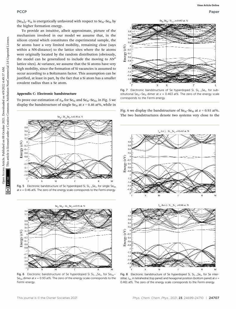
To prove our estimation of xM for SeSi and SeSi–SeSi, in Fig. 5 wedisplay the bandstructure of single SeSi at x = 0.46 at%, while in
Fig. 6 we display the bandstructure of SeSi–SeSi at x = 0.93 at%.The two bandstructures denote two systems very close to the
Fig. 5 Electronic bandstructure of Se hyperdoped Si, Si1�xSex, for single SeSe
at x = 0.46 at%. The zero of the energy scale corresponds to the Fermi energy.
Fig. 6 Electronic bandstructure of Se hyperdoped Si Si1�xSex, for SeSe–SeSe dimer at x = 0.93 at%. The zero of the energy scale corresponds to theFermi energy.
Fig. 7 Electronic bandstructure of Se hyperdoped Si, Si1�xSex, for sub-stitutional SeSi–SeSi dimer at x = 0.463 at%. The zero of the energy scalecorresponds to the Fermi energy.
Fig. 8 Electronic bandstructure of Se hyperdoped Si, Si1�xSex, for Se inter-stitial, ISe, in tetrahedral (top panel) and hexagonal position (bottom panel) at x =0.461 at%. The zero of the energy scale corresponds to the Fermi energy.
PCCP Paper
Ope
n A
cces
s A
rtic
le. P
ublis
hed
on 0
8 O
ctob
er 2
021.
Dow
nloa
ded
on 4
/9/2
022
4:49
:37
AM
. T
his
artic
le is
lice
nsed
und
er a
Cre
ativ
e C
omm
ons
Attr
ibut
ion-
Non
Com
mer
cial
3.0
Unp
orte
d L
icen
ce.
View Article Online

24708 | Phys. Chem. Chem. Phys., 2021, 23, 24699–24710 This journal is © the Owner Societies 2021
semi-metallic state in which the conduction band minimum isbasically equal to the maximum of the impurity band.
For completeness, by using the same Se concentration wecomputed the DOS displayed in Section III.B, for each type ofdefect we provide the electronic bandstructure, along highsymmetry direction in the Brillouin zone (labels along highsymmetry directions the Brillouin zone has been assignedaccording to the symmetry of the super-cell used in the simulation,see Appendix A for further details).
In Fig. 7 we display, the electronic bandstructure of SeSi–SeSi
for x = 0.463 at%. At variance with bandstructure of the samecomplex for x = 0.93 at% displayed in Fig. 6, at the lowerconcentration of x = 0.463 at%, the IB is still separated by theconduction band.
In Fig. 8 we display the electronic bandstructure of Seinterstitials. For ISe in the tetrahedral position we cannotice the partially filled IB, which is situated deep in thebandgap, thus acting as an acceptor defect. At variance, at theconsidered concentration, the IB of ISe in hexagonal position, ismerged into the conduction band, as can be noticed by looking
at the bandstructure along the G–X direction in theBrillouin zone.
In Fig. 9 and 10 we display the electronic bandstructure ofthe complexes (SeSi)m–VSi, m = 1, 2, 3, and 4. As discussed in themain text, at x C 0.465 at%, the (SeSi)1–VSi is an acceptorcomplex, and it is characterized by a partially filled IB in themiddle of the gap. At variance at x C 0.438 at%, the IB of(SeSi)3–VSi is fully merged into the conduction band. As can benoticed by looking at the figures, the considered concentrations(SeSi)2–VSi and (SeSi)4–VSi have shallow IBs, and these complexesact as donors. The bandstructures illustrated above provide acomplementary picture of the analysis of electronic propertiesof the different types of defects discussed in Section III.B bymeans of the DOS.
Appendix D: Formation energy of a couple of substitutional Se
To support the assumption of a random distribution of Sedopants at the different lattice sites of silicon, used in AppendixB to provide a quantitative estimation of the concentration ofthe different types of defects, we considered the formation
Fig. 9 Electronic bandstructure of Se hyperdoped Si, Si1�xSex, for (SeSi)1–VSi at x C 0.465 at% (top panel), and for (SeSi)2–VSi at x C 0.464 at%(bottom panel). The zero of the energy scale corresponds to the Fermienergy.
Fig. 10 Electronic bandstructure of Se hyperdoped Si, Si1�xSex, for(SeSi)3–VSi at x C 0.438 at% (top panel), and for (SeSi)4–VSi at x C 0.463at% (bottom panel). The zero of the energy scale corresponds to the Fermienergy.
Paper PCCP
Ope
n A
cces
s A
rtic
le. P
ublis
hed
on 0
8 O
ctob
er 2
021.
Dow
nloa
ded
on 4
/9/2
022
4:49
:37
AM
. T
his
artic
le is
lice
nsed
und
er a
Cre
ativ
e C
omm
ons
Attr
ibut
ion-
Non
Com
mer
cial
3.0
Unp
orte
d L
icen
ce.
View Article Online
This journal is © the Owner Societies 2021 Phys. Chem. Chem. Phys., 2021, 23, 24699–24710 | 24709
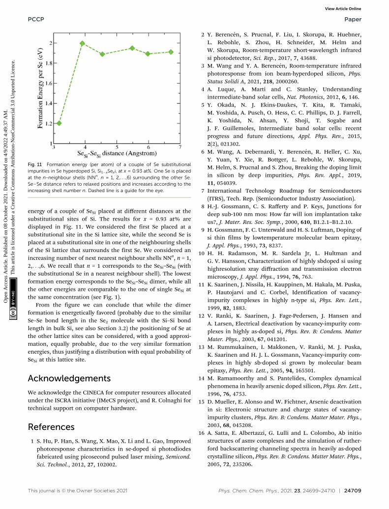
energy of a couple of SeSi placed at different distances at thesubstitutional sites of Si. The results for x = 0.93 at% aredisplayed in Fig. 11. We considered the first Se placed at asubstitutional site in the Si lattice site, while the second Se isplaced at a substitutional site in one of the neighbouring shellsof the Si lattice that surrounds the first Se. We considered anincreasing number of next nearest neighbour shells NNn, n = 1,2,. . .,6. We recall that n = 1 corresponds to the SeSi–SeSi (withthe substitutional Se in a nearest neighbour shell). The lowestformation energy corresponds to the SeSi–SeSi dimer, while allthe other energies are comparable to the one of single SeSi atthe same concentration (see Fig. 1).
From the figure we can conclude that while the dimerformation is energetically favored (probably due to the similarSe–Se bond length in the Se2 molecule with the Si–Si bondlength in bulk Si, see also Section 3.2) the positioning of Se atthe other lattice sites can be considered, with a good approxi-mation, equally probable, due to the very similar formationenergies, thus justifying a distribution with equal probability ofSeSi at this lattice site.
Acknowledgements
We acknowledge the CINECA for computer resources allocatedunder the ISCRA initiative (IMeCS project), and R. Colnaghi fortechnical support on computer hardware.
References
1 S. Hu, P. Han, S. Wang, X. Mao, X. Li and L. Gao, Improvedphotoresponse characteristics in se-doped si photodiodesfabricated using picosecond pulsed laser mixing, Semicond.Sci. Technol., 2012, 27, 102002.
2 Y. Berencen, S. Prucnal, F. Liu, I. Skorupa, R. Huebner,L. Rebohle, S. Zhou, H. Schneider, M. Helm andW. Skorupa, Room-temperature short-wavelength infraredsi photodetector, Sci. Rep., 2017, 7, 43688.
3 M. Wang and Y. A. Berencen, Room-temperature infraredphotoresponse from ion beam-hyperdoped silicon, Phys.Status Solidi A, 2021, 218, 2000260.
4 A. Luque, A. Marti and C. Stanley, Understandingintermediate-band solar cells, Nat. Photonics, 2012, 6, 146.
5 Y. Okada, N. J. Ekins-Daukes, T. Kita, R. Tamaki,M. Yoshida, A. Pusch, O. Hess, C. C. Phillips, D. J. Farrell,K. Yoshida, N. Ahsan, Y. Shoji, T. Sogabe andJ. F. Guillemoles, Intermediate band solar cells: recentprogress and future directions, Appl. Phys. Rev., 2015,2(2), 021302.
6 M. Wang, A. Debernardi, Y. Berencen, R. Heller, C. Xu,Y. Yuan, Y. Xie, R. Bottger, L. Rebohle, W. Skorupa,M. Helm, S. Prucnal and S. Zhou, Breaking the doping limitin silicon by deep impurities, Phys. Rev. Appl., 2019,11, 054039.
7 International Technology Roadmap for Semiconductors(ITRS), Tech. Rep. (Semiconductor Industry Association).
8 H.-J. Gossmann, C. S. Rafferty and P. Keys, Junctions fordeep sub-100 nm mos: How far will ion implantation takeus?, J. Mater. Res. Soc. Symp., 2000, 610, B1.2.1–B1.2.10.
9 H. Gossmann, F. C. Unterwald and H. S. Luftman, Doping ofsi thin films by lowtemperature molecular beam epitaxy,J. Appl. Phys., 1993, 73, 8237.
10 H. H. Radamson, M. R. Sardela Jr, L. Hultman andG. V. Hansson, Characterization of highly sbdoped si usinghighresolution xray diffraction and transmission electronmicroscopy, J. Appl. Phys., 1994, 76, 763.
11 K. Saarinen, J. Nissila, H. Kauppinen, M. Hakala, M. Puska,P. Hautojarvi and C. Corbel, Identification of vacancy-impurity complexes in highly n-type si, Phys. Rev. Lett.,1999, 82, 1883.
12 V. Ranki, K. Saarinen, J. Fage-Pedersen, J. Hansen andA. Larsen, Electrical deactivation by vacancy-impurity com-plexes in highly as-doped si, Phys. Rev. B: Condens. MatterMater. Phys., 2003, 67, 041201.
13 M. Rummukainen, I. Makkonen, V. Ranki, M. J. Puska,K. Saarinen and H. J. L. Gossmann, Vacancy-impurity com-plexes in highly sb-doped si grown by molecular beamepitaxy, Phys. Rev. Lett., 2005, 94, 165501.
14 M. Ramamoorthy and S. Pantelides, Complex dynamicalphenomena in heavily arsenic doped silicon, Phys. Rev. Lett.,1996, 76, 4753.
15 D. Mueller, E. Alonso and W. Fichtner, Arsenic deactivationin si: Electronic structure and charge states of vacancy-impurity clusters, Phys. Rev. B: Condens. Matter Mater. Phys.,2003, 68, 045208.
16 A. Satta, E. Albertazzi, G. Lulli and L. Colombo, Ab initiostructures of asmv complexes and the simulation of ruther-ford backscattering channeling spectra in heavily as-dopedcrystalline silicon, Phys. Rev. B: Condens. Matter Mater. Phys.,2005, 72, 235206.
Fig. 11 Formation energy (per atom) of a couple of Se substitutionalimpurities in Se hyperdoped Si, Si1�xSexi, at x = 0.93 at%. One Se is placedat the n-neighbour shells (NNn, n = 1, 2,. . .,6) surrounding the other Se.Se–Se distance refers to relaxed positions and increases according to theincreasing shell number n. Dashed line is a guide for the eye.
PCCP Paper
Ope
n A
cces
s A
rtic
le. P
ublis
hed
on 0
8 O
ctob
er 2
021.
Dow
nloa
ded
on 4
/9/2
022
4:49
:37
AM
. T
his
artic
le is
lice
nsed
und
er a
Cre
ativ
e C
omm
ons
Attr
ibut
ion-
Non
Com
mer
cial
3.0
Unp
orte
d L
icen
ce.
View Article Online

24710 | Phys. Chem. Chem. Phys., 2021, 23, 24699–24710 This journal is © the Owner Societies 2021
17 D. Mathiot and J. C. Pfister, Diffusion of arsenic in silicon:validity of the percolation model, Appl. Phys. Lett., 1983, 42,1043–1044.
18 D. Mathiot and J. C. Pfister, Dopant diffusion in silicon: aconsistent view involving nonequilibrium defects, J. Appl.Phys., 1984, 55, 3518.
19 K. Pandey, A. Erbil, G. Cargill, R. Boehme and D. Vanderbilt,Annealing of heavily arsenic-doped silicon: Electrical deac-tivation and a new defect complex, Phys. Rev. Lett., 1988, 61,1282–1285.
20 D. Lawther, U. Myler, P. Simpson, P. Rousseau, P. Griffinand J. Plummer, Vacancy generation resulting from electri-cal deactivation of arsenic, Appl. Phys. Lett., 1995, 67,3575–3577.
21 V. Ranki, J. Nissila and K. Saarinen, Formation of vacancy-impurity complexes by kinetic processes in highly as-dopedsi, Phys. Rev. Lett., 2002, 88, 105506.
22 V. Ranki and K. Saarinen, Formation of thermal vacancies inhighly as and p doped si, Phys. Rev. Lett., 2004, 93, 255502.
23 R. Pinacho, M. Jaraiz, P. Castrillo, I. Martin-Bragado,J. Rubio and J. Barbolla, Modeling arsenic deactivationthrough arsenic-vacancy clusters using an atomistic kineticmonte carlo approach, Appl. Phys. Lett., 2005, 86, 252103.
24 P. Voyles, D. Muller, J. Grazul, P. Citrin and H. Gossmann,Atomic-scale imaging of individual dopant atoms and clus-ters in highly n-type bulk si, Nature, 2002, 416, 826.
25 D. Mueller and W. Fichtner, Highly n-doped silicon: Deac-tivating defects of donors, Phys. Rev. B: Condens. MatterMater. Phys., 2004, 70, 245207.
26 D. Chadi, P. Citrin, C. Park, D. Adler, M. Marcus andH. Gossmann, Fermi-level-pinning defects in highly n-doped silicon, Phys. Rev. Lett., 1997, 79, 4834.
27 M. T. Winkler, D. Recht, M.-J. Sher, A. J. Said, E. Mazur andM. J. Aziz, Insulator-to-metal transition in sulfur-dopedsilicon, Phys. Rev. Lett., 2011, 106, 178701.
28 E. Ertekin, M. T. Winkler, D. Recht, A. J. Said, M. J. Aziz,T. Buonassisi and J. C. Grossman, Insulator-to-metal transi-tion in selenium-hyperdoped silicon: Observation and ori-gin, Phys. Rev. Lett., 2012, 108, 026401.
29 M. Wang, A. Debernardi, W. Zhang, C. Xu, Y. Yuan, Y. Xie,Y. Berencen, S. Prucnal, M. Helm and S. Zhou, Criticalbehavior of the insulator-to-metal transition in Te-hyperdoped si, Phys. Rev. B: Condens. Matter Mater. Phys.,2020, 102, 085204.
30 K. Suzuki, Y. Tada, Y. Kataoka, K. Kawamura, T. Nagayama,S. Nagayama, C. W. Magee, T. H. Bueyueklimanli, D. C. Mueller,W. Fichtner and C. Zechner, Maximum active concentration ofion-implanted phosphorus during solid-phase epitaxial recrys-tallization, IEEE Trans. Electron Devices, 2007, 54, 1985.
31 Z.-Y. Zhao and P.-Z. A. Yang, Insight into insulator-to-metaltransition of sulfur-doped silicon by dft calculations, Phys.Chem. Chem. Phys., 2014, 16, 17499.
32 S. Zhou, F. Liu, S. Prucnal, K. Gao, M. Khalid, C. Baehtz,M. Posselt, W. Skorupa and M. K. Helm, Hyperdopingsilicon with selenium: solid vs. liquid phase epitaxy, Sci.Rep., 2015, 5, 8329.
33 F. Liu, S. Prucnal, Y. Berencen, Z. Zhang, Y. Yuan, Y. Liu,R. Heller, R. Boettger, L. Rebohle, W. Skorupa, M. Helm andS. Zhou, Realizing the insulator-to-metal transition in se-hyperdoped si via non-equilibrium material processing,J. Phys. D: Appl. Phys., 2017, 50, 415102.
34 See e.g., H. Overhof, M. Scheffler and C. M. Weinert, For-mation energies, electronic structure, and hyperfine fieldsof chalcogen point defects and defect pairs in silicon, Phys.Rev. B: Condens. Matter Mater. Phys., 1991, 43, 12494, andreferences therein.
35 P. Giannozzi, S. Baroni, N. Bonini, M. Calandra, R. Car,C. Cavazzoni, D. Ceresoli, G. L. Chiarotti, M. Cococcioni,I. Dabo, A. D. Corso, S. Fabris, G. Fratesi, S. de Gironcoli,R. Gebauer, U. Gerstmann, C. Gougoussis, A. Kokalj,M. Lazzeri, L. Martin-Samos, N. Marzari, F. Mauri,R. Mazzarello, S. Paolini, A. Pasquarello, L. Paulatto,C. Sbraccia, S. Scandolo, G. Sclauzero, A. P. Seitsonen,A. Smogunov, P. Umari and R. M. Wentzcovitch, Quantumespresso: a modular and open-source software project forquantum simulations of materials, J. Phys.: Condens. Matter,2009, 21, 395502.
36 A. M. Rappe, K. M. Rabe, E. Kaxiras and J. D. Joannopoulos,Optimized pseudopotentials, Phys. Rev. B: Condens. MatterMater. Phys., 1990, 41, 1227(R).
37 D. Vanderbilt, Soft self-consistent pseudopotentials in ageneralized eigenvalue formalism, Phys. Rev. B: Condens.Matter Mater. Phys., 1990, 41, 7892(R).
38 L. Kleinmann and D. Bylander, Efficacious form for modelpseudopotentials, Phys. Rev. Lett., 1982, 48, 1425.
39 J. P. Perdew, K. Burke and M. Ernzerhof, Generalizedgradient approximation made simple, Phys. Rev. Lett.,1996, 77, 3865; J. P. Perdew, K. Burke and M. Ernzerhof,Generalized gradient approximation made simple, Phys.Rev. Lett., 1997, 78, 1396(E).
40 R. W. Wyckoff, Crystal Structures, Wiley Interscience Pub-lication, New York, 1971, vol. 1.
41 H. J. Monkhorst and J. D. Pack, Special points for brillouin-zone integration, Phys. Rev. B: Condens. Matter Mater. Phys.,1976, 13, 5188.
42 G. Petretto, A. Debernardi and M. Fanciulli, Confinementeffects and hyperfine structure in se doped silicon nano-wires, Nano Lett., 2011, 11, 4509.
Paper PCCP
Ope
n A
cces
s A
rtic
le. P
ublis
hed
on 0
8 O
ctob
er 2
021.
Dow
nloa
ded
on 4
/9/2
022
4:49
:37
AM
. T
his
artic
le is
lice
nsed
und
er a
Cre
ativ
e C
omm
ons
Attr
ibut
ion-
Non
Com
mer
cial
3.0
Unp
orte
d L
icen
ce.
View Article Online