Embed Size (px)
Citation preview
VCC
GND
VCMLP FWPWR_END2+ D2– D1+ D1–
ReferenceGenerator
VREF
Copyright © 2016, Texas Instruments Incorporated
Product
Folder
Sample &Buy
Technical
Documents
Tools &
Software
Support &Community
An IMPORTANT NOTICE at the end of this data sheet addresses availability, warranty, changes, use in safety-critical applications,intellectual property matters and other important disclaimers. PRODUCTION DATA.
TPD4S1394SLVSA55B –NOVEMBER 2009–REVISED NOVEMBER 2016
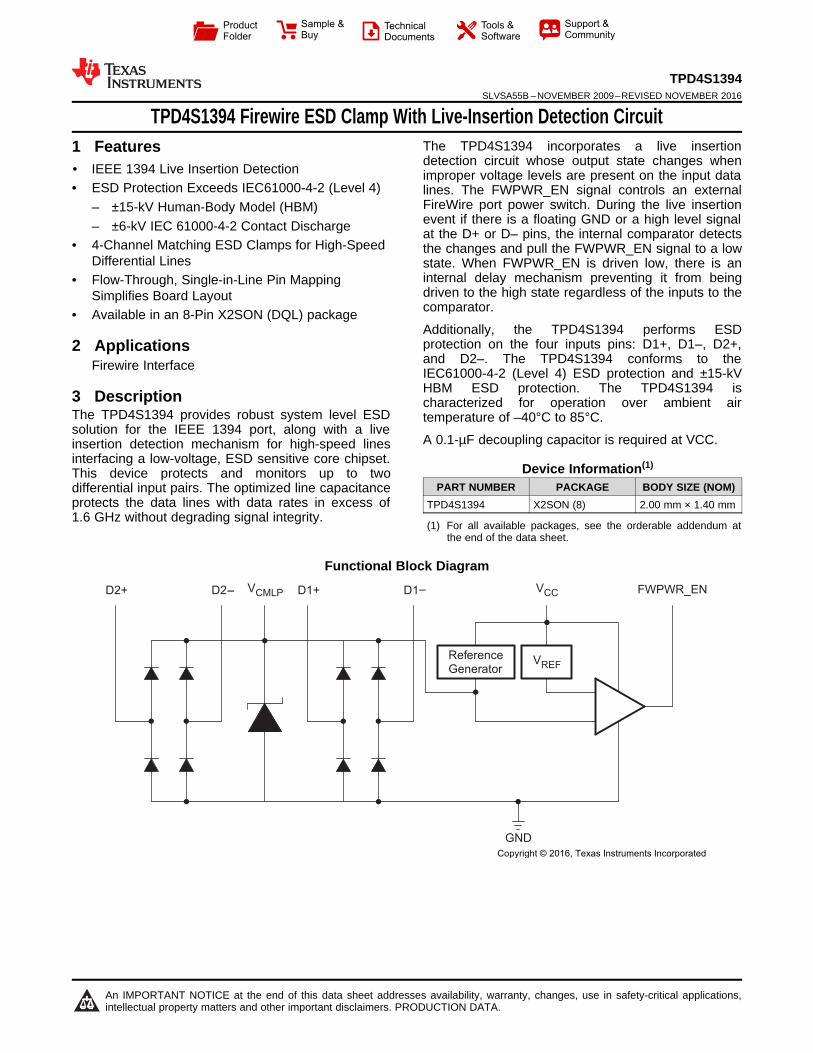
TPD4S1394 Firewire ESD Clamp With Live-Insertion Detection Circuit
1
1 Features1• IEEE 1394 Live Insertion Detection• ESD Protection Exceeds IEC61000-4-2 (Level 4)
– ±15-kV Human-Body Model (HBM)– ±6-kV IEC 61000-4-2 Contact Discharge
• 4-Channel Matching ESD Clamps for High-SpeedDifferential Lines
• Flow-Through, Single-in-Line Pin MappingSimplifies Board Layout
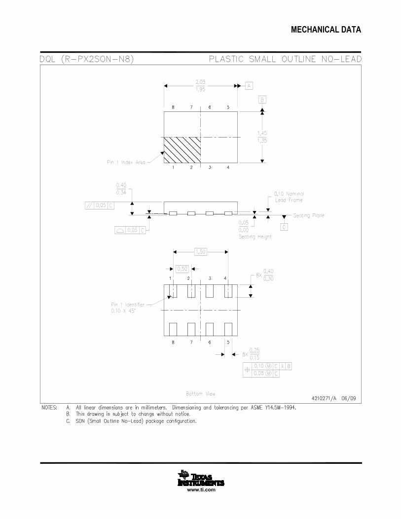
• Available in an 8-Pin X2SON (DQL) package
2 ApplicationsFirewire Interface
3 DescriptionThe TPD4S1394 provides robust system level ESDsolution for the IEEE 1394 port, along with a liveinsertion detection mechanism for high-speed linesinterfacing a low-voltage, ESD sensitive core chipset.This device protects and monitors up to twodifferential input pairs. The optimized line capacitanceprotects the data lines with data rates in excess of1.6 GHz without degrading signal integrity.
The TPD4S1394 incorporates a live insertiondetection circuit whose output state changes whenimproper voltage levels are present on the input datalines. The FWPWR_EN signal controls an externalFireWire port power switch. During the live insertionevent if there is a floating GND or a high level signalat the D+ or D– pins, the internal comparator detectsthe changes and pull the FWPWR_EN signal to a lowstate. When FWPWR_EN is driven low, there is aninternal delay mechanism preventing it from beingdriven to the high state regardless of the inputs to thecomparator.
Additionally, the TPD4S1394 performs ESDprotection on the four inputs pins: D1+, D1–, D2+,and D2–. The TPD4S1394 conforms to theIEC61000-4-2 (Level 4) ESD protection and ±15-kVHBM ESD protection. The TPD4S1394 ischaracterized for operation over ambient airtemperature of –40°C to 85°C.
A 0.1-µF decoupling capacitor is required at VCC.
Device Information(1)
PART NUMBER PACKAGE BODY SIZE (NOM)TPD4S1394 X2SON (8) 2.00 mm × 1.40 mm
(1) For all available packages, see the orderable addendum atthe end of the data sheet.
Functional Block Diagram
2
TPD4S1394SLVSA55B –NOVEMBER 2009–REVISED NOVEMBER 2016 www.ti.com
Product Folder Links: TPD4S1394
Submit Documentation Feedback Copyright © 2009–2016, Texas Instruments Incorporated
Table of Contents1 Features .................................................................. 12 Applications ........................................................... 13 Description ............................................................. 14 Revision History..................................................... 25 Pin Configuration and Functions ......................... 36 Specifications......................................................... 3
6.1 Absolute Maximum Ratings ...................................... 36.2 ESD Ratings.............................................................. 36.3 Recommended Operating Conditions....................... 46.4 Thermal Information .................................................. 46.5 Electrical Characteristics........................................... 46.6 Switching Characteristics .......................................... 46.7 Typical Characteristics .............................................. 5
7 Detailed Description .............................................. 67.1 Overview ................................................................... 67.2 Functional Block Diagram ......................................... 6
7.3 Feature Description................................................... 67.4 Device Functional Modes.......................................... 6
8 Application and Implementation .......................... 78.1 Application Information.............................................. 78.2 Typical Application .................................................... 7
9 Power Supply Recommendations ........................ 810 Layout..................................................................... 8
10.1 Layout Guidelines ................................................... 810.2 Layout Example ...................................................... 9
11 Device and Documentation Support ................. 1011.1 Receiving Notification of Documentation Updates 1011.2 Community Resources.......................................... 1011.3 Trademarks ........................................................... 1011.4 Electrostatic Discharge Caution............................ 1011.5 Glossary ................................................................ 10
12 Mechanical, Packaging, and OrderableInformation ........................................................... 10
4 Revision HistoryNOTE: Page numbers for previous revisions may differ from page numbers in the current version.
Changes from Revision A (March 2013) to Revision B Page
• Added Device Information table, Pin Configuration and Functions section, Specifications section, ESD Ratings table,Switching Characteristics table, Detailed Description section, Application and Implementation section, Power SupplyRecommendations section, Layout section, Device and Documentation Support section, and Mechanical,Packaging, and Orderable Information section ...................................................................................................................... 1
• Added Thermal Information table ........................................................................................................................................... 4
Changes from Original (November 2009) to Revision A Page
• Removed hard coded ordering information table. Information contained in Package Orderable Addendum. ....................... 1
1
2
3
4
VCC
GND
VCMLP
FWPWR_EN
D1+
D1–
D2+
D2–
8
7
6
5
3
TPD4S1394www.ti.com SLVSA55B –NOVEMBER 2009–REVISED NOVEMBER 2016
Product Folder Links: TPD4S1394
Submit Documentation FeedbackCopyright © 2009–2016, Texas Instruments Incorporated
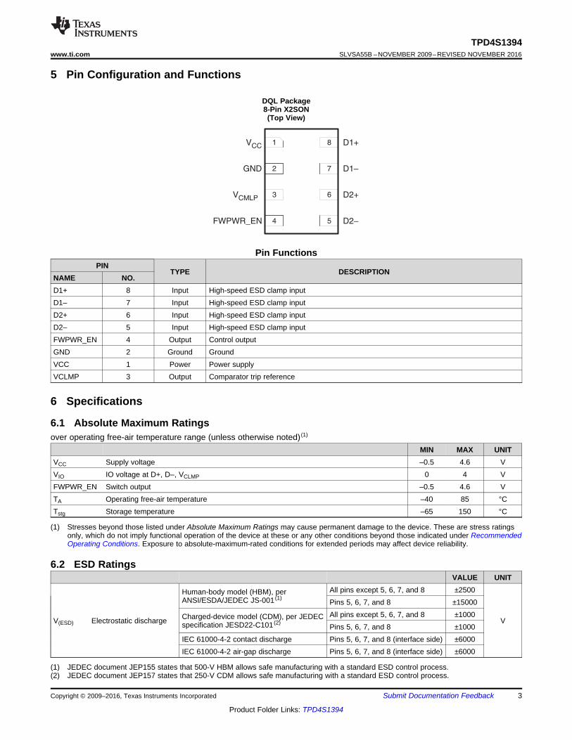
5 Pin Configuration and Functions
DQL Package8-Pin X2SON(Top View)
Pin FunctionsPIN
TYPE DESCRIPTIONNAME NO.D1+ 8 Input High-speed ESD clamp inputD1– 7 Input High-speed ESD clamp inputD2+ 6 Input High-speed ESD clamp inputD2– 5 Input High-speed ESD clamp inputFWPWR_EN 4 Output Control outputGND 2 Ground GroundVCC 1 Power Power supplyVCLMP 3 Output Comparator trip reference
(1) Stresses beyond those listed under Absolute Maximum Ratings may cause permanent damage to the device. These are stress ratingsonly, which do not imply functional operation of the device at these or any other conditions beyond those indicated under RecommendedOperating Conditions. Exposure to absolute-maximum-rated conditions for extended periods may affect device reliability.
6 Specifications
6.1 Absolute Maximum Ratingsover operating free-air temperature range (unless otherwise noted) (1)
MIN MAX UNITVCC Supply voltage –0.5 4.6 VVIO IO voltage at D+, D–, VCLMP 0 4 VFWPWR_EN Switch output –0.5 4.6 VTA Operating free-air temperature –40 85 °CTstg Storage temperature –65 150 °C
(1) JEDEC document JEP155 states that 500-V HBM allows safe manufacturing with a standard ESD control process.(2) JEDEC document JEP157 states that 250-V CDM allows safe manufacturing with a standard ESD control process.
6.2 ESD RatingsVALUE UNIT
V(ESD) Electrostatic discharge
Human-body model (HBM), perANSI/ESDA/JEDEC JS-001 (1)
All pins except 5, 6, 7, and 8 ±2500
V
Pins 5, 6, 7, and 8 ±15000
Charged-device model (CDM), per JEDECspecification JESD22-C101 (2)
All pins except 5, 6, 7, and 8 ±1000Pins 5, 6, 7, and 8 ±1000
IEC 61000-4-2 contact discharge Pins 5, 6, 7, and 8 (interface side) ±6000IEC 61000-4-2 air-gap discharge Pins 5, 6, 7, and 8 (interface side) ±6000

4
TPD4S1394SLVSA55B –NOVEMBER 2009–REVISED NOVEMBER 2016 www.ti.com
Product Folder Links: TPD4S1394
Submit Documentation Feedback Copyright © 2009–2016, Texas Instruments Incorporated
6.3 Recommended Operating Conditionsover operating free-air temperature range (unless otherwise noted)
PARAMETER MIN MAX UNITVCC Supply voltage 3 3.6 V
(1) For more information about traditional and new thermal metrics, see the Semiconductor and IC Package Thermal Metrics applicationreport.
6.4 Thermal Information
THERMAL METRIC (1)TPD4S1394
UNITDQL (X2SON)8 PINS
RθJA Junction-to-ambient thermal resistance 167.5 °C/WRθJC(top) Junction-to-case (top) thermal resistance 56.8 °C/WRθJB Junction-to-board thermal resistance 82.3 °C/WψJT Junction-to-top characterization parameter 1.5 °C/WψJB Junction-to-board characterization parameter 82 °C/W
(1) A 0.1-µF decoupling capacitor is required at VCC.
6.5 Electrical Characteristicsover operating free-air temperature range (unless otherwise noted) (1)
PARAMETER TEST CONDITIONS MIN TYP MAX UNIT
VDXFWPWR_EN trip voltage(D+ and D– pins)
High-to-low 2.9 3.4 4V
Low-to-high 2.7 3.2 3.8VCLMP Value on pin No connection 2.45 VVBR Breakdown voltage at VCLAMP II = 1 mA 4.2 VVD Diode forward voltage for lower clamp ID = 8 mA lower clamp diode –0.6 –0.8 –0.95 VFWPWR_EN Switch output VCC VRDYN Dynamic resistance (in and out clamp) of D+, D– I = 1 A 1 Ω
CIO I/O capacitance of D+, D– VIO = 2.5 V 1.5 2 pFICC Current consumption VCC = 3.3 V, FWPWR_EN = high 130 200 µA
6.6 Switching Characteristicsover operating free-air temperature range (unless otherwise noted)
PARAMETER TEST CONDITIONS MIN TYP MAX UNITtTRIP Delay time for FWPWR_EN to go low Loading on FWPWR_EN = 50 pF 0.5 2 5 µstRESET Delay time for FWPWR_EN to go high after trip FWPWR_EN = VCC 300 450 600 ms

-18
-15
-12
-9
-6
-3
0
1.0E+07 1.0E+08 1.0E+09 1.0E+10
Frequency (Hz)
Inse
rtio
n L
oss (
dB
) -3.0 dB Frequency = 2.4 GHz
0.0
0.5
1.0
1.5
2.0
2.5
0.0 0.5 1.0 1.5 2.0 2.5 3.0 3.5
Voltage Bias (V)
Ca
pa
cita
nce
(p
F)
5
TPD4S1394www.ti.com SLVSA55B –NOVEMBER 2009–REVISED NOVEMBER 2016
Product Folder Links: TPD4S1394
Submit Documentation FeedbackCopyright © 2009–2016, Texas Instruments Incorporated
6.7 Typical Characteristics
D+, D– Pins
Figure 1. I/O Capacitance vs I/O Voltage
D+, D– Pins
Figure 2. Insertion Loss (S21)
VCC
GND
VCMLP FWPWR_END2+ D2– D1+ D1–
ReferenceGenerator
VREF
Copyright © 2016, Texas Instruments Incorporated
6
TPD4S1394SLVSA55B –NOVEMBER 2009–REVISED NOVEMBER 2016 www.ti.com
Product Folder Links: TPD4S1394
Submit Documentation Feedback Copyright © 2009–2016, Texas Instruments Incorporated
7 Detailed Description
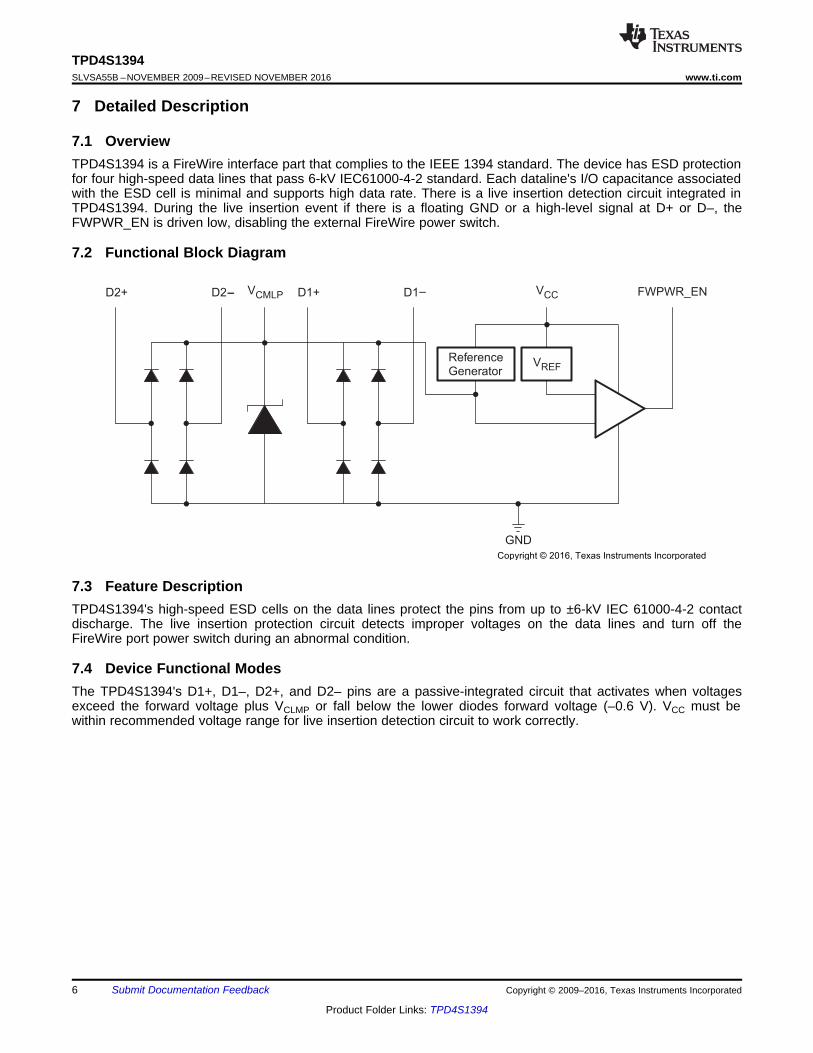
7.1 OverviewTPD4S1394 is a FireWire interface part that complies to the IEEE 1394 standard. The device has ESD protectionfor four high-speed data lines that pass 6-kV IEC61000-4-2 standard. Each dataline's I/O capacitance associatedwith the ESD cell is minimal and supports high data rate. There is a live insertion detection circuit integrated inTPD4S1394. During the live insertion event if there is a floating GND or a high-level signal at D+ or D–, theFWPWR_EN is driven low, disabling the external FireWire power switch.
7.2 Functional Block Diagram
7.3 Feature DescriptionTPD4S1394's high-speed ESD cells on the data lines protect the pins from up to ±6-kV IEC 61000-4-2 contactdischarge. The live insertion protection circuit detects improper voltages on the data lines and turn off theFireWire port power switch during an abnormal condition.
7.4 Device Functional ModesThe TPD4S1394's D1+, D1–, D2+, and D2– pins are a passive-integrated circuit that activates when voltagesexceed the forward voltage plus VCLMP or fall below the lower diodes forward voltage (–0.6 V). VCC must bewithin recommended voltage range for live insertion detection circuit to work correctly.
FirewireConnector
PowerPower Switch
GND
FWPWR_EN
TPD1394
TPB±
TPB+
TPA±
TPA+
TPB±_SYS
TPB+_SYS
TPA±_SYS
TPA+_SYS
Copyright © 2016, Texas Instruments Incorporated
7
TPD4S1394www.ti.com SLVSA55B –NOVEMBER 2009–REVISED NOVEMBER 2016
Product Folder Links: TPD4S1394
Submit Documentation FeedbackCopyright © 2009–2016, Texas Instruments Incorporated
8 Application and Implementation
NOTEInformation in the following applications sections is not part of the TI componentspecification, and TI does not warrant its accuracy or completeness. TI’s customers areresponsible for determining suitability of components for their purposes. Customers shouldvalidate and test their design implementation to confirm system functionality.
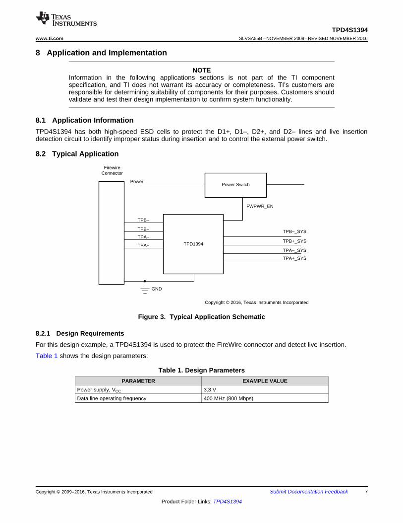
8.1 Application InformationTPD4S1394 has both high-speed ESD cells to protect the D1+, D1–, D2+, and D2– lines and live insertiondetection circuit to identify improper status during insertion and to control the external power switch.
8.2 Typical Application
Figure 3. Typical Application Schematic
8.2.1 Design RequirementsFor this design example, a TPD4S1394 is used to protect the FireWire connector and detect live insertion.
Table 1 shows the design parameters:
Table 1. Design ParametersPARAMETER EXAMPLE VALUE
Power supply, VCC 3.3 VData line operating frequency 400 MHz (800 Mbps)

-18
-15
-12
-9
-6
-3
0
1.0E+07 1.0E+08 1.0E+09 1.0E+10
Frequency (Hz)
Insert
ion L
oss (
dB
) -3.0 dB Frequency = 2.4 GHz
0.0
0.5
1.0
1.5
2.0
2.5
0.0 0.5 1.0 1.5 2.0 2.5 3.0 3.5
Voltage Bias (V)
Capacitance (
pF
)
8
TPD4S1394SLVSA55B –NOVEMBER 2009–REVISED NOVEMBER 2016 www.ti.com
Product Folder Links: TPD4S1394
Submit Documentation Feedback Copyright © 2009–2016, Texas Instruments Incorporated
8.2.2 Detailed Design ProcedureThe data transfer rate of 800 Mbps is well below the bandwidth of the data pins of TPD4S1394. So the parasiticsassociated with the ESD cells on these lines do not degrade the signal integrity. 3.3-V power supplies arecommonly available from the board and can be used to power the live insertion detection circuit.
8.2.3 Application Curves
D+, D– Pins
Figure 4. I/O Capacitance vs I/O Voltage
D+, D– Pins
Figure 5. Insertion Loss (S21)
9 Power Supply RecommendationsTI recommends a power supply for VCC is from 3 V to 3.6 V.
10 Layout
10.1 Layout Guidelines• The optimum placement is as close to the connector as possible.
– EMI during an ESD event can couple from the trace being struck to other nearby unprotected traces,resulting in early system failures.
– The PCB designer must minimize the possibility of EMI coupling by keeping any unprotected traces awayfrom the protected traces which are between the TVS and the connector.
• Route the protected traces as straight as possible.• Eliminate any sharp corners on the protected traces between the TVS and the connector by using rounded
corners with the largest radii possible.– Electric fields tend to build up on corners, increasing EMI coupling.

1
2
3
4 5
6
7
8
Via to power ground plane Via to power supply plane
VCC
GND
VCLAMP
FWPWR_EN
D1+
D1–
D2+
D2–
9
TPD4S1394www.ti.com SLVSA55B –NOVEMBER 2009–REVISED NOVEMBER 2016
Product Folder Links: TPD4S1394
Submit Documentation FeedbackCopyright © 2009–2016, Texas Instruments Incorporated
10.2 Layout Example
Figure 6. TPD4S1394 Layout Example

10
TPD4S1394SLVSA55B –NOVEMBER 2009–REVISED NOVEMBER 2016 www.ti.com
Product Folder Links: TPD4S1394
Submit Documentation Feedback Copyright © 2009–2016, Texas Instruments Incorporated
11 Device and Documentation Support
11.1 Receiving Notification of Documentation UpdatesTo receive notification of documentation updates, navigate to the device product folder on ti.com. In the upperright corner, click on Alert me to register and receive a weekly digest of any product information that haschanged. For change details, review the revision history included in any revised document.
11.2 Community ResourcesThe following links connect to TI community resources. Linked contents are provided "AS IS" by the respectivecontributors. They do not constitute TI specifications and do not necessarily reflect TI's views; see TI's Terms ofUse.
TI E2E™ Online Community TI's Engineer-to-Engineer (E2E) Community. Created to foster collaborationamong engineers. At e2e.ti.com, you can ask questions, share knowledge, explore ideas and helpsolve problems with fellow engineers.
Design Support TI's Design Support Quickly find helpful E2E forums along with design support tools andcontact information for technical support.
11.3 TrademarksE2E is a trademark of Texas Instruments.All other trademarks are the property of their respective owners.
11.4 Electrostatic Discharge CautionThis integrated circuit can be damaged by ESD. Texas Instruments recommends that all integrated circuits be handled withappropriate precautions. Failure to observe proper handling and installation procedures can cause damage.
ESD damage can range from subtle performance degradation to complete device failure. Precision integrated circuits may be moresusceptible to damage because very small parametric changes could cause the device not to meet its published specifications.
11.5 GlossarySLYZ022 — TI Glossary.
This glossary lists and explains terms, acronyms, and definitions.
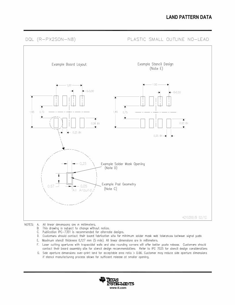
12 Mechanical, Packaging, and Orderable InformationThe following pages include mechanical, packaging, and orderable information. This information is the mostcurrent data available for the designated devices. This data is subject to change without notice and revision ofthis document. For browser-based versions of this data sheet, refer to the left-hand navigation.

PACKAGE OPTION ADDENDUM
www.ti.com 2-Mar-2016
Addendum-Page 1
PACKAGING INFORMATION
Orderable Device Status(1)
Package Type PackageDrawing
Pins PackageQty
Eco Plan(2)
Lead/Ball Finish(6)
MSL Peak Temp(3)
Op Temp (°C) Device Marking(4/5)
Samples
TPD4S1394DQLR ACTIVE X2SON DQL 8 3000 Green (RoHS& no Sb/Br)
CU NIPDAU Level-1-260C-UNLIM -40 to 85 (5J7 ~ 5JR)
(1) The marketing status values are defined as follows:ACTIVE: Product device recommended for new designs.LIFEBUY: TI has announced that the device will be discontinued, and a lifetime-buy period is in effect.NRND: Not recommended for new designs. Device is in production to support existing customers, but TI does not recommend using this part in a new design.PREVIEW: Device has been announced but is not in production. Samples may or may not be available.OBSOLETE: TI has discontinued the production of the device.
(2) Eco Plan - The planned eco-friendly classification: Pb-Free (RoHS), Pb-Free (RoHS Exempt), or Green (RoHS & no Sb/Br) - please check http://www.ti.com/productcontent for the latest availabilityinformation and additional product content details.TBD: The Pb-Free/Green conversion plan has not been defined.Pb-Free (RoHS): TI's terms "Lead-Free" or "Pb-Free" mean semiconductor products that are compatible with the current RoHS requirements for all 6 substances, including the requirement thatlead not exceed 0.1% by weight in homogeneous materials. Where designed to be soldered at high temperatures, TI Pb-Free products are suitable for use in specified lead-free processes.Pb-Free (RoHS Exempt): This component has a RoHS exemption for either 1) lead-based flip-chip solder bumps used between the die and package, or 2) lead-based die adhesive used betweenthe die and leadframe. The component is otherwise considered Pb-Free (RoHS compatible) as defined above.Green (RoHS & no Sb/Br): TI defines "Green" to mean Pb-Free (RoHS compatible), and free of Bromine (Br) and Antimony (Sb) based flame retardants (Br or Sb do not exceed 0.1% by weightin homogeneous material)
(3) MSL, Peak Temp. - The Moisture Sensitivity Level rating according to the JEDEC industry standard classifications, and peak solder temperature.
(4) There may be additional marking, which relates to the logo, the lot trace code information, or the environmental category on the device.
(5) Multiple Device Markings will be inside parentheses. Only one Device Marking contained in parentheses and separated by a "~" will appear on a device. If a line is indented then it is a continuationof the previous line and the two combined represent the entire Device Marking for that device.
(6) Lead/Ball Finish - Orderable Devices may have multiple material finish options. Finish options are separated by a vertical ruled line. Lead/Ball Finish values may wrap to two lines if the finishvalue exceeds the maximum column width.
Important Information and Disclaimer:The information provided on this page represents TI's knowledge and belief as of the date that it is provided. TI bases its knowledge and belief on informationprovided by third parties, and makes no representation or warranty as to the accuracy of such information. Efforts are underway to better integrate information from third parties. TI has taken andcontinues to take reasonable steps to provide representative and accurate information but may not have conducted destructive testing or chemical analysis on incoming materials and chemicals.TI and TI suppliers consider certain information to be proprietary, and thus CAS numbers and other limited information may not be available for release.
In no event shall TI's liability arising out of such information exceed the total purchase price of the TI part(s) at issue in this document sold by TI to Customer on an annual basis.
PACKAGE OPTION ADDENDUM
www.ti.com 2-Mar-2016
Addendum-Page 2
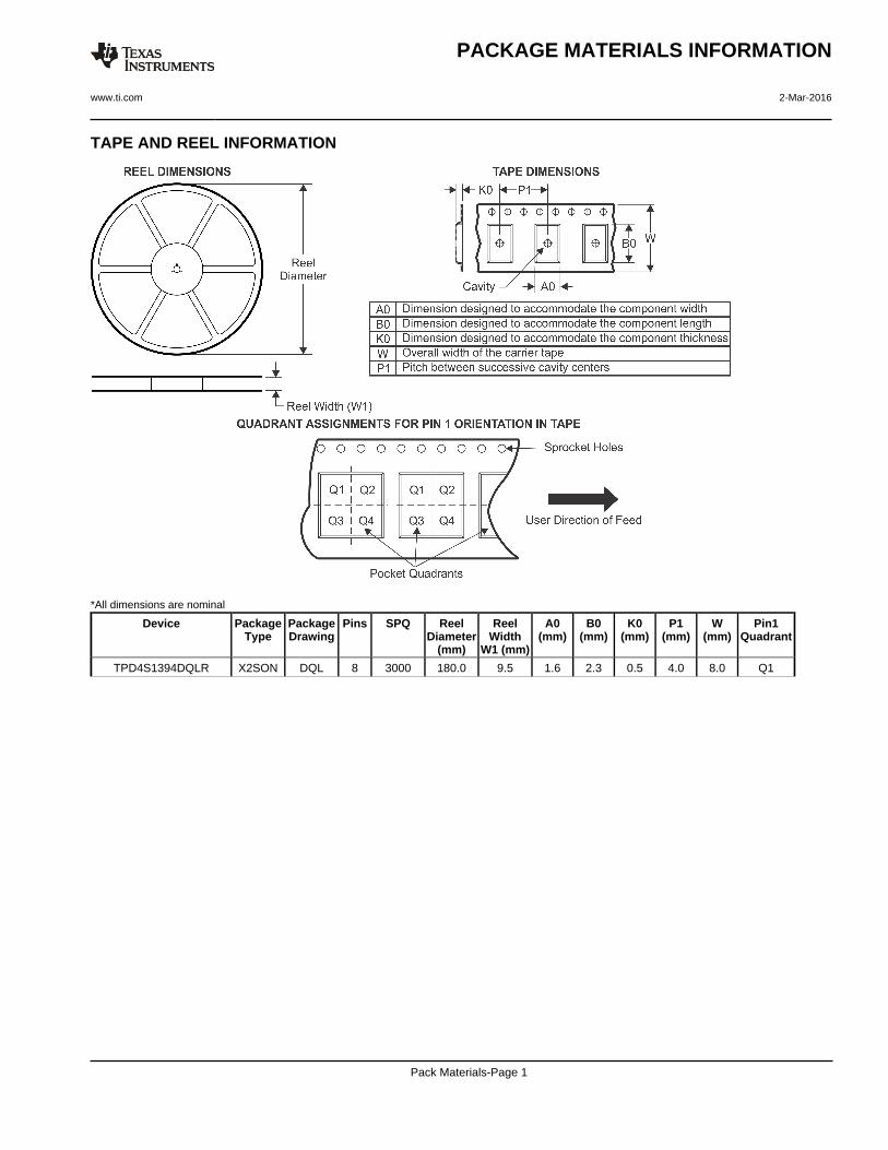
TAPE AND REEL INFORMATION
*All dimensions are nominal
Device PackageType
PackageDrawing
Pins SPQ ReelDiameter
(mm)
ReelWidth
W1 (mm)
A0(mm)
B0(mm)
K0(mm)
P1(mm)
W(mm)
Pin1Quadrant
TPD4S1394DQLR X2SON DQL 8 3000 180.0 9.5 1.6 2.3 0.5 4.0 8.0 Q1
PACKAGE MATERIALS INFORMATION
www.ti.com 2-Mar-2016
Pack Materials-Page 1
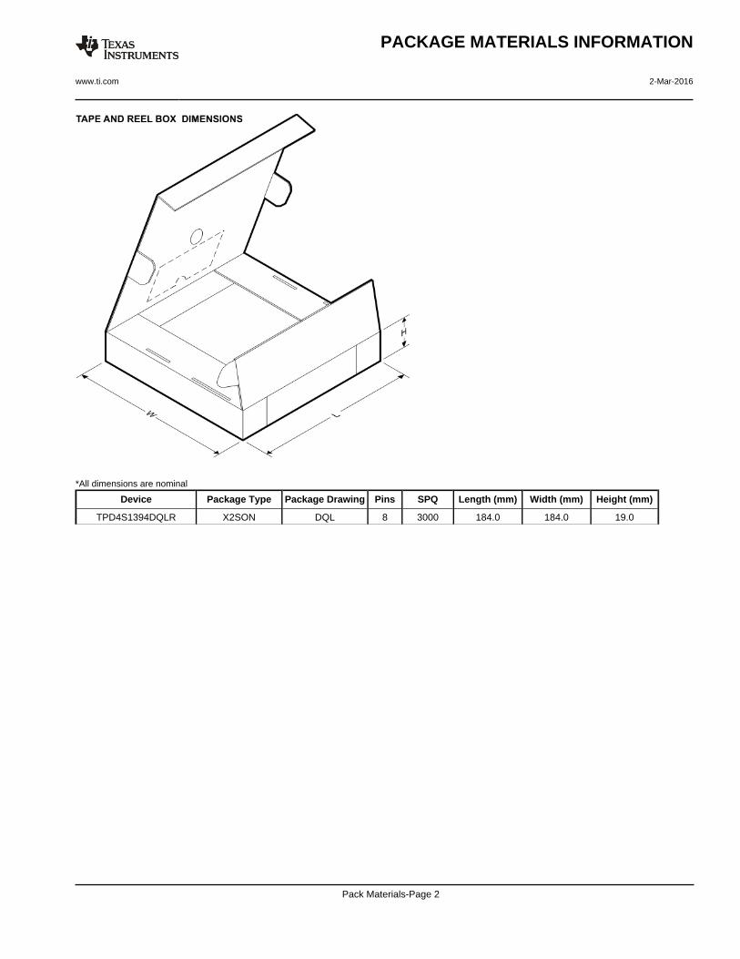
*All dimensions are nominal
Device Package Type Package Drawing Pins SPQ Length (mm) Width (mm) Height (mm)
TPD4S1394DQLR X2SON DQL 8 3000 184.0 184.0 19.0
PACKAGE MATERIALS INFORMATION
www.ti.com 2-Mar-2016
Pack Materials-Page 2
IMPORTANT NOTICE
Texas Instruments Incorporated and its subsidiaries (TI) reserve the right to make corrections, enhancements, improvements and otherchanges to its semiconductor products and services per JESD46, latest issue, and to discontinue any product or service per JESD48, latestissue. Buyers should obtain the latest relevant information before placing orders and should verify that such information is current andcomplete. All semiconductor products (also referred to herein as “components”) are sold subject to TI’s terms and conditions of salesupplied at the time of order acknowledgment.TI warrants performance of its components to the specifications applicable at the time of sale, in accordance with the warranty in TI’s termsand conditions of sale of semiconductor products. Testing and other quality control techniques are used to the extent TI deems necessaryto support this warranty. Except where mandated by applicable law, testing of all parameters of each component is not necessarilyperformed.TI assumes no liability for applications assistance or the design of Buyers’ products. Buyers are responsible for their products andapplications using TI components. To minimize the risks associated with Buyers’ products and applications, Buyers should provideadequate design and operating safeguards.TI does not warrant or represent that any license, either express or implied, is granted under any patent right, copyright, mask work right, orother intellectual property right relating to any combination, machine, or process in which TI components or services are used. Informationpublished by TI regarding third-party products or services does not constitute a license to use such products or services or a warranty orendorsement thereof. Use of such information may require a license from a third party under the patents or other intellectual property of thethird party, or a license from TI under the patents or other intellectual property of TI.Reproduction of significant portions of TI information in TI data books or data sheets is permissible only if reproduction is without alterationand is accompanied by all associated warranties, conditions, limitations, and notices. TI is not responsible or liable for such altereddocumentation. Information of third parties may be subject to additional restrictions.Resale of TI components or services with statements different from or beyond the parameters stated by TI for that component or servicevoids all express and any implied warranties for the associated TI component or service and is an unfair and deceptive business practice.TI is not responsible or liable for any such statements.Buyer acknowledges and agrees that it is solely responsible for compliance with all legal, regulatory and safety-related requirementsconcerning its products, and any use of TI components in its applications, notwithstanding any applications-related information or supportthat may be provided by TI. Buyer represents and agrees that it has all the necessary expertise to create and implement safeguards whichanticipate dangerous consequences of failures, monitor failures and their consequences, lessen the likelihood of failures that might causeharm and take appropriate remedial actions. Buyer will fully indemnify TI and its representatives against any damages arising out of the useof any TI components in safety-critical applications.In some cases, TI components may be promoted specifically to facilitate safety-related applications. With such components, TI’s goal is tohelp enable customers to design and create their own end-product solutions that meet applicable functional safety standards andrequirements. Nonetheless, such components are subject to these terms.No TI components are authorized for use in FDA Class III (or similar life-critical medical equipment) unless authorized officers of the partieshave executed a special agreement specifically governing such use.Only those TI components which TI has specifically designated as military grade or “enhanced plastic” are designed and intended for use inmilitary/aerospace applications or environments. Buyer acknowledges and agrees that any military or aerospace use of TI componentswhich have not been so designated is solely at the Buyer's risk, and that Buyer is solely responsible for compliance with all legal andregulatory requirements in connection with such use.TI has specifically designated certain components as meeting ISO/TS16949 requirements, mainly for automotive use. In any case of use ofnon-designated products, TI will not be responsible for any failure to meet ISO/TS16949.
Products ApplicationsAudio www.ti.com/audio Automotive and Transportation www.ti.com/automotiveAmplifiers amplifier.ti.com Communications and Telecom www.ti.com/communicationsData Converters dataconverter.ti.com Computers and Peripherals www.ti.com/computersDLP® Products www.dlp.com Consumer Electronics www.ti.com/consumer-appsDSP dsp.ti.com Energy and Lighting www.ti.com/energyClocks and Timers www.ti.com/clocks Industrial www.ti.com/industrialInterface interface.ti.com Medical www.ti.com/medicalLogic logic.ti.com Security www.ti.com/securityPower Mgmt power.ti.com Space, Avionics and Defense www.ti.com/space-avionics-defenseMicrocontrollers microcontroller.ti.com Video and Imaging www.ti.com/videoRFID www.ti-rfid.comOMAP Applications Processors www.ti.com/omap TI E2E Community e2e.ti.comWireless Connectivity www.ti.com/wirelessconnectivity
Mailing Address: Texas Instruments, Post Office Box 655303, Dallas, Texas 75265Copyright © 2016, Texas Instruments Incorporated