Embed Size (px)
Citation preview
Finite State Machines (FSMs) and RAMs and
inner workings of CPUs COS 116, Spring 2010Guest: Szymon Rusinkiewicz
Recap
• Combinational logic circuits: no cycles, hence no “memory”
• Sequential circuits: cycles allowed; can have memory as well as “undefined”/ambiguous behavior
• Clocked sequential circuits: Contain D flip flops whose“Write” input is controlled by a clock signal
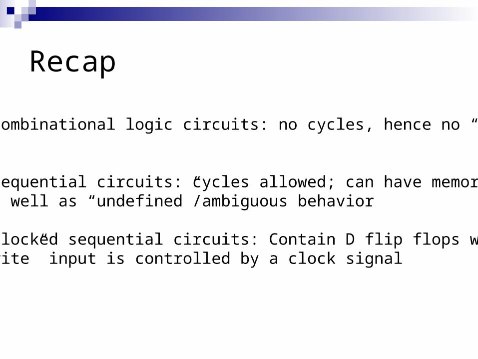
R-S Flip-Flop(corrected slide)
S
R
M
Forbidden toturn on bothSet and Resetsimultaneously(value is“ambiguous”)
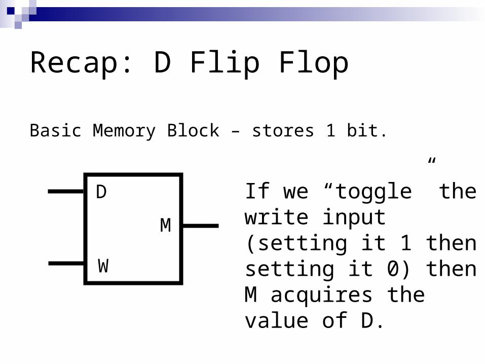
Recap: D Flip Flop
Basic Memory Block – stores 1 bit.
D
W
M
If we “toggle” the write input (setting it 1 then setting it 0) then M acquires the value of D.
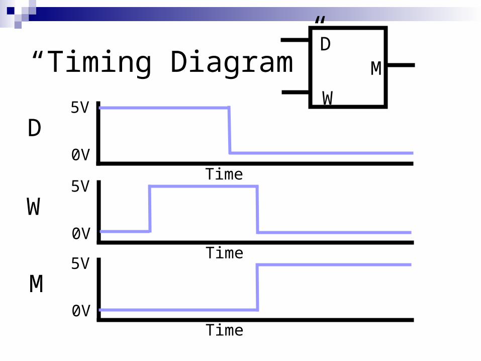
“Timing Diagram”5V
0VTime
D
5V
0VTime
W
5V
0VTime
M
D
W
M
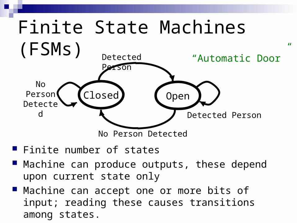
Finite State Machines (FSMs)
Finite number of states Machine can produce outputs, these depend upon
current state only Machine can accept one or more bits of input; reading
these causes transitions among states.
Closed Open
Detected Person
No Person
DetectedDetected Person
No Person Detected
“Automatic Door”
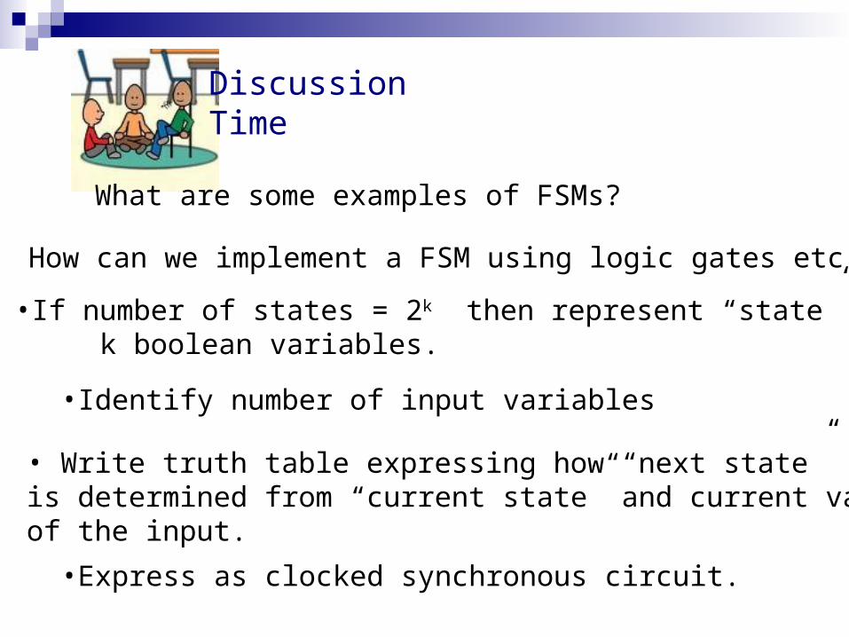
Discussion Time
How can we implement a FSM using logic gates etc.?
•If number of states = 2k then represent “state” byk boolean variables.
•Identify number of input variables
• Write truth table expressing how “next state” is determined from “current state” and current valuesof the input.
•Express as clocked synchronous circuit.
What are some examples of FSMs?
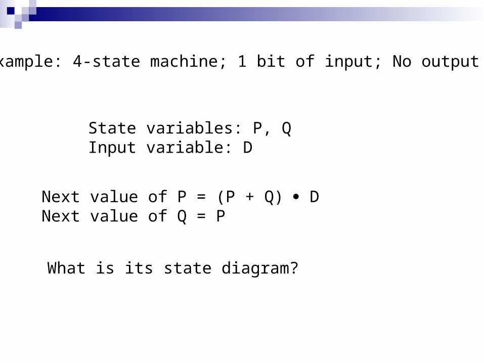
Example: 4-state machine; 1 bit of input; No output
State variables: P, QInput variable: D
Next value of P = (P + Q) DNext value of Q = P
What is its state diagram?
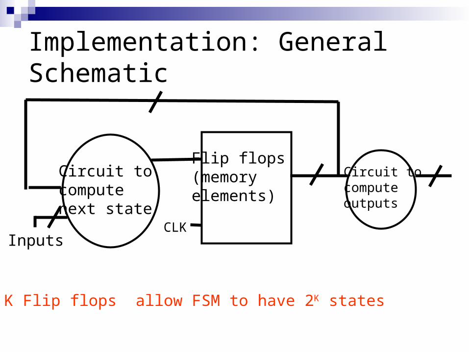
Implementation: General Schematic
Inputs
Circuit to computenext state
Flip flops(memoryelements)
Circuit tocomputeoutputs
CLK
K Flip flops allow FSM to have 2K states
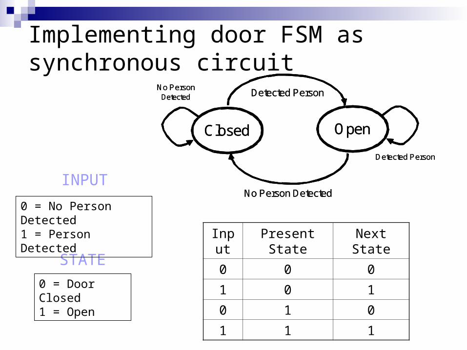
Implementing door FSM as synchronous circuit
INPUT
STATE
0 = No Person Detected1 = Person Detected
0 = Door Closed1 = Open
Closed Open
Detected PersonNo Person
Detected
Detected Person
No Person Detected
Closed Open
Detected PersonNo Person
Detected
Detected Person
No Person Detected
Input Present State Next State
0 0 0
1 0 1
0 1 0
1 1 1
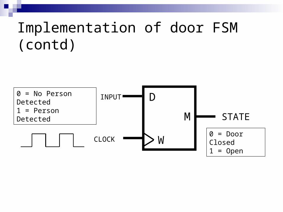
Implementation of door FSM (contd)
D
W
M
INPUT
CLOCK
0 = No Person Detected1 = Person Detected
0 = Door Closed1 = Open
STATE
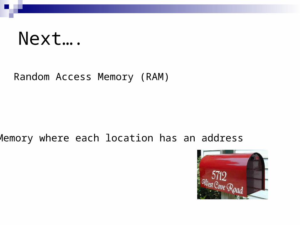
Next….
Random Access Memory (RAM)
Memory where each location has an address
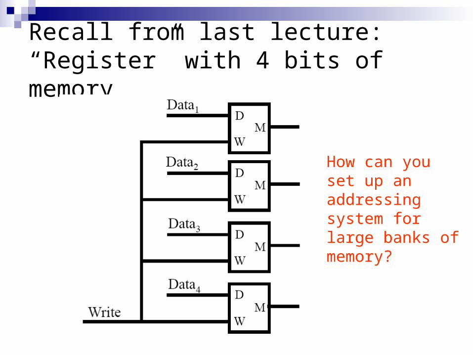
Recall from last lecture: “Register” with 4 bits of memory
How can youset up an addressingsystem for large banks of memory?
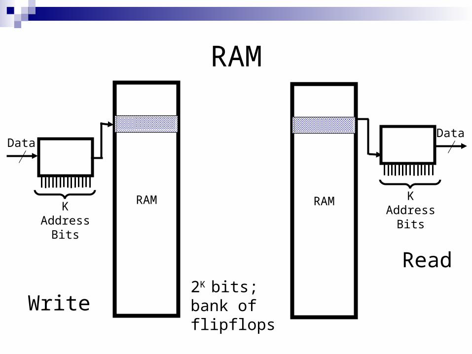
RAM
RAM
2K bits;bank offlipflops
K Address Bits
Data
Write
RAM K Address Bits
Data
Read
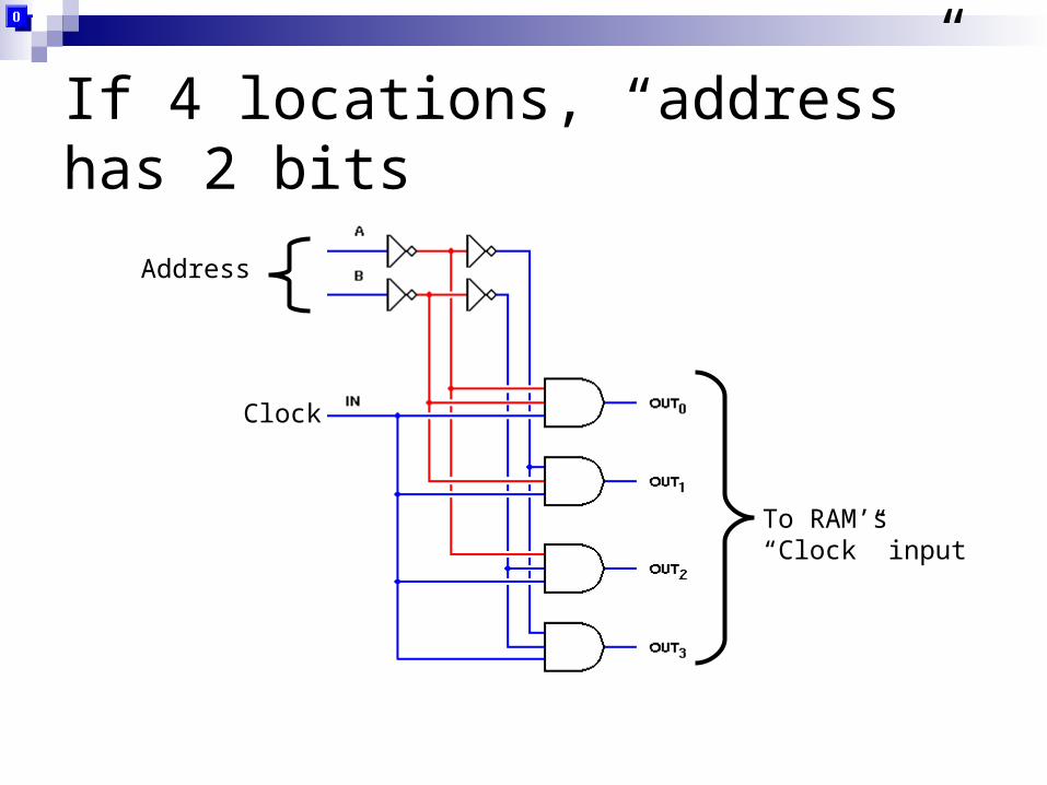
If 4 locations, “address” has 2 bits
Address
Clock
To RAM’s“Clock” input
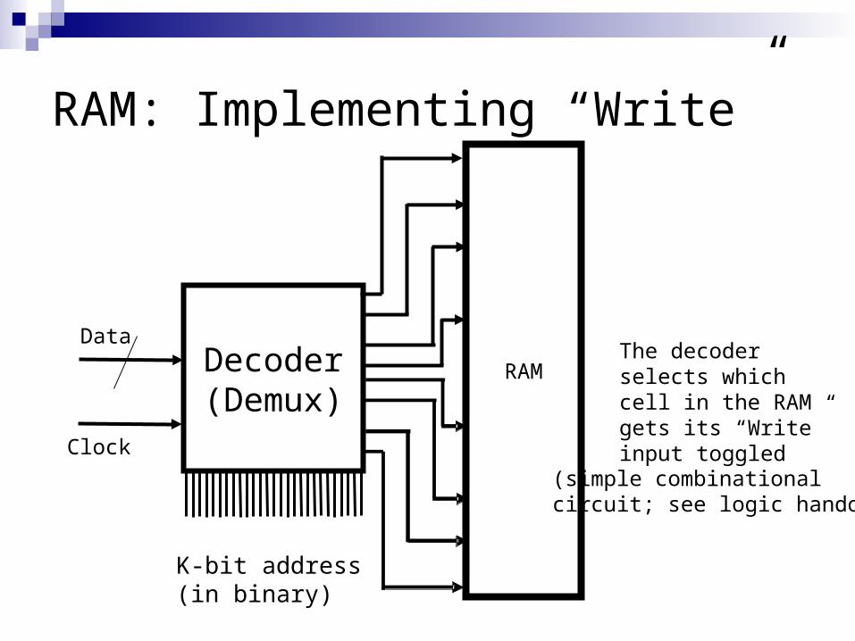
RAM: Implementing “Write”
RAMDecoder(Demux)
DataThe decoder selects which cell in the RAM gets its “Write” input toggled
K-bit address(in binary)
Clock
(simple combinationalcircuit; see logic handout)
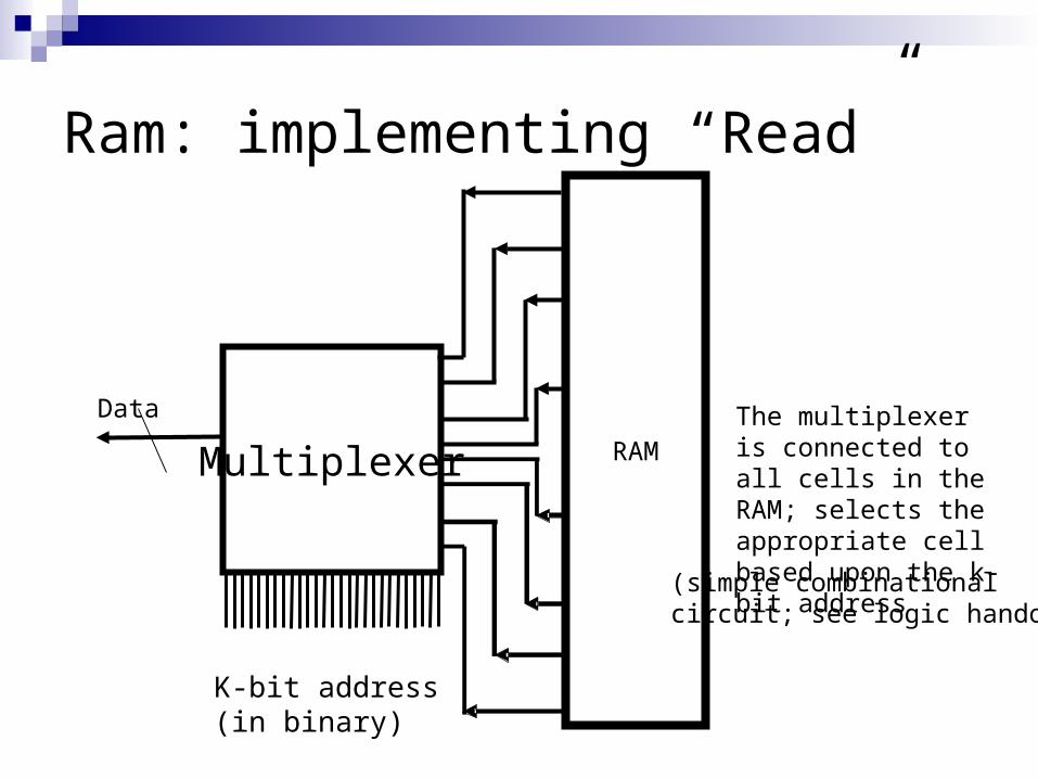
Ram: implementing “Read”
RAMMultiplexer
Data The multiplexer is connected to all cells in the RAM; selects the appropriate cell based upon the k-bit address
K-bit address(in binary)
(simple combinationalcircuit; see logic handout)
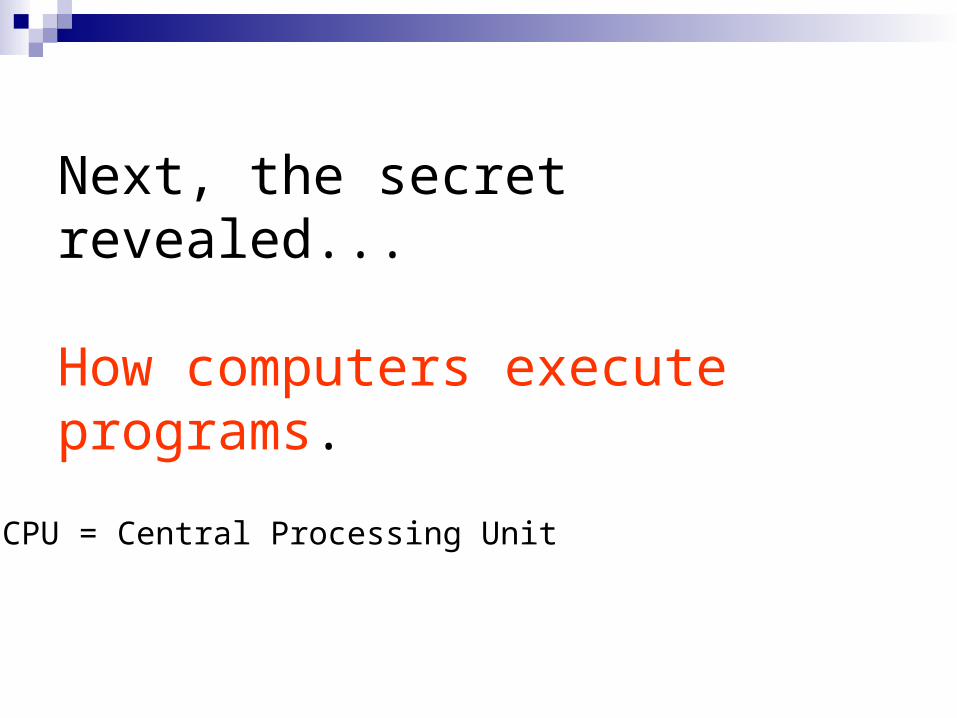
Next, the secret revealed...
How computers execute programs.
CPU = Central Processing Unit
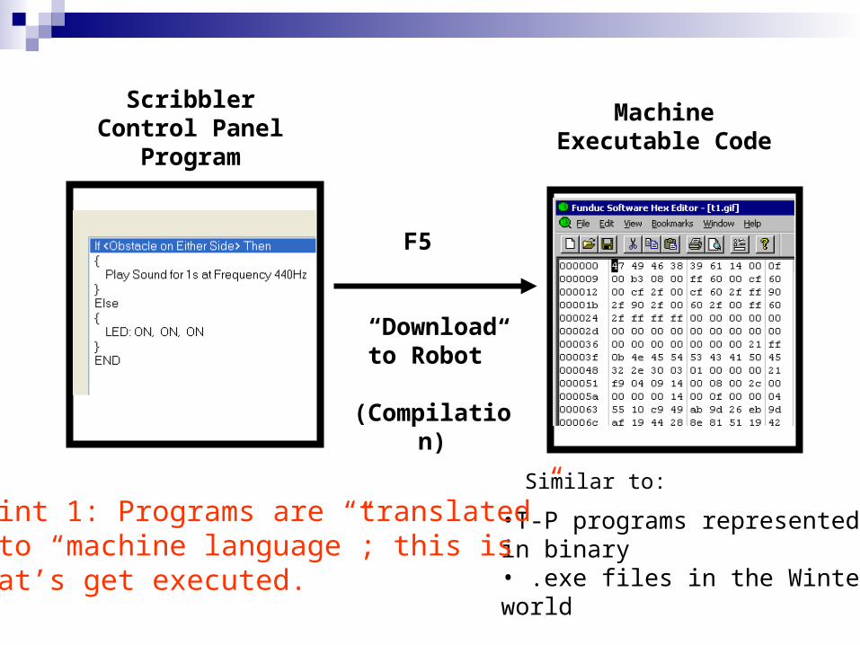
Scribbler Control Panel Program
Machine Executable Code
F5
“Download to Robot”
(Compilation)
•T-P programs representedin binary• .exe files in the Wintel world
Similar to:
Point 1: Programs are “translated”into “machine language”; this iswhat’s get executed.
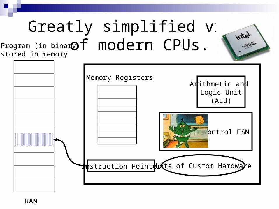
Greatly simplified view of modern CPUs.Program (in binary)
stored in memory
Memory RegistersArithmetic and
Logic Unit(ALU)
Control FSM
Lots of Custom HardwareInstruction Pointer
RAM
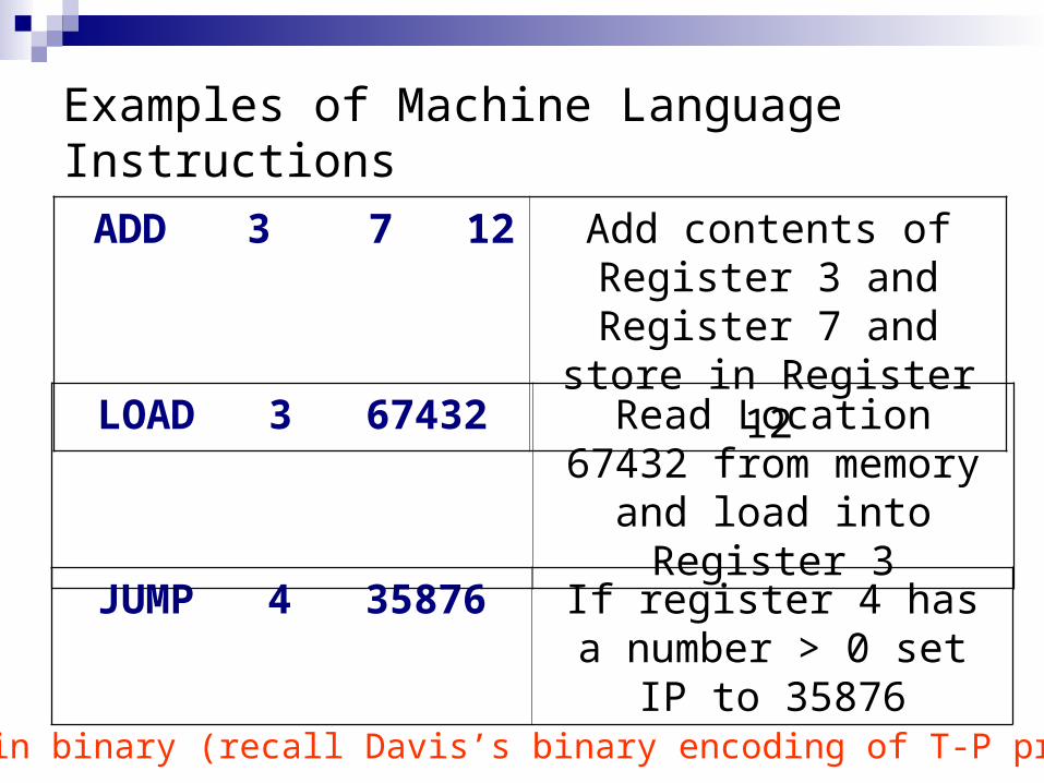
Examples of Machine Language Instructions
ADD 3 7 12 Add contents of Register 3 and Register 7 and store in Register 12
JUMP 4 35876 If register 4 has a number > 0 set IP to
35876
LOAD 3 67432 Read Location 67432 from memory and load
into Register 3
Stored in binary (recall Davis’s binary encoding of T-P programs)
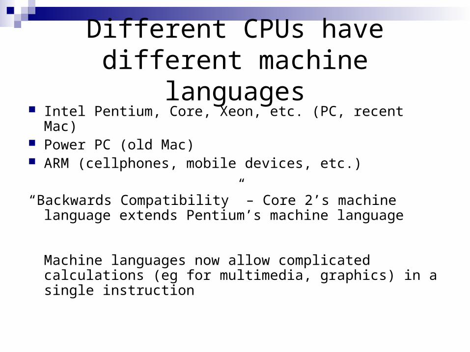
Different CPUs have different machine languages
Intel Pentium, Core, Xeon, etc. (PC, recent Mac) Power PC (old Mac) ARM (cellphones, mobile devices, etc.)
“Backwards Compatibility” – Core 2’s machine language extends Pentium’s machine language
Machine languages now allow complicated calculations (eg for multimedia, graphics) in a single instruction
Main Insight
Computer = FSM controlling a larger (or infinite) memory.
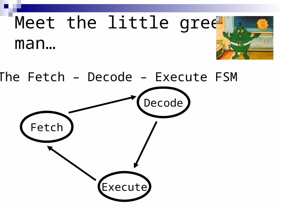
Meet the little green man…
The Fetch – Decode – Execute FSM
Execute
Decode
Fetch
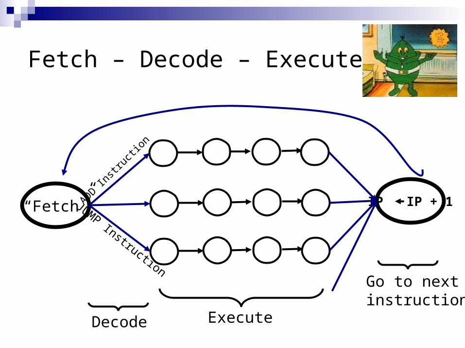
Fetch – Decode – Execute FSM
“Fetch” IP IP + 1
Decode Execute
ADD Instr
uctio
n
JUMP Instruction
Go to nextinstruction
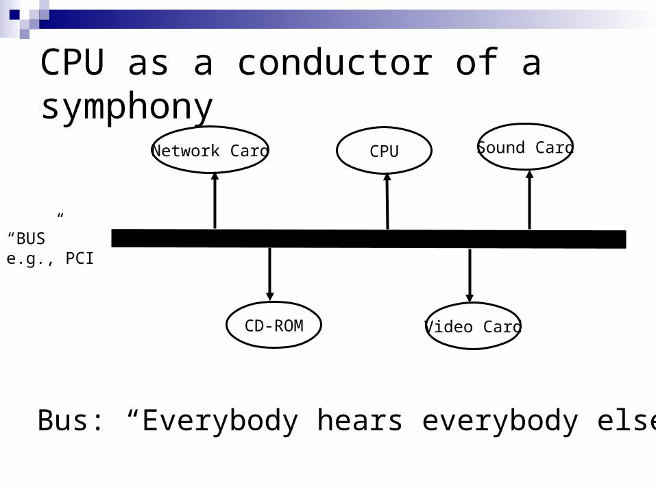
CPU as a conductor of a symphony
Network Card CPU Sound Card
CD-ROM Video Card
“BUS” e.g., PCI
Bus: “Everybody hears everybody else”
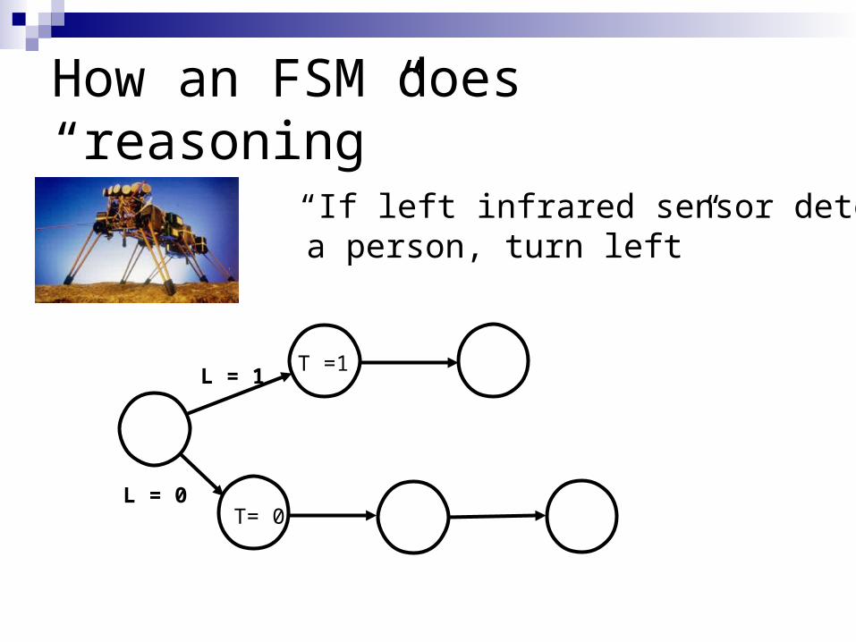
How an FSM does “reasoning”
“If left infrared sensor detects a person, turn left”
L = 0
L = 1T =1
T= 0
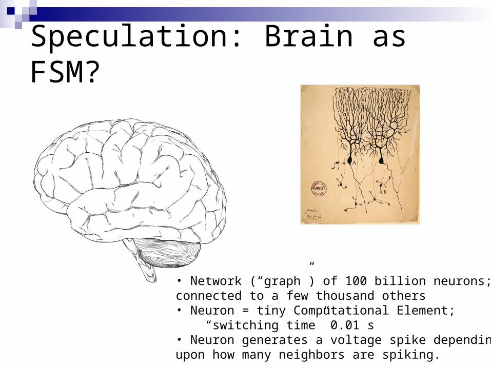
Speculation: Brain as FSM?
• Network (“graph”) of 100 billion neurons; each connected to a few thousand others• Neuron = tiny Computational Element; “switching time” 0.01 s• Neuron generates a voltage spike depending upon how many neighbors are spiking.