Embed Size (px)
Citation preview
ECE 2020 Lab 2: Finite State Machine Lab
©Bonnie H. Ferri, School of Electrical and Computer Engineering, Georgia Tech, [email protected]
1
Finite State Machine Module: Lab Procedures Goal: The goal of this experiment is to reinforce state machine concepts by having students design and implement a state machine using simple chips and a protoboard. This experiment also introduces students to basic physical components. Contents:
Background Page 1 Prelab Page 6 Experiment Page 8 Appendix Page 11
Background: The general steps to be followed for performing state machine design include: 1) Convert a description of the problem into a state transition diagram 2) Transfer the information from the state transition diagram to a state transition logic table that has inputs consisting of system inputs and current values of the state, Si, and outputs consisting of system outputs and next state values, NSi. 3) Design a combination circuit to implement the logic in the table. 4) Select the chips to implement the combinational circuit and to implement the memory portion of the state machine, for example, D flip flops can be used to implement registers. 5) Draw a pin diagram to illustrate how to wire the chips together to implement the state machine logic. 6) Insert the chips into a protoboard and wire the ground, high voltage, enables, and clock pins. 7) Complete the circuit by making the connections indicated from Step 5). 8) Test the circuit. Notation and Definitions: States: A = 00, B = 01, C = 10, D =11 where the states are defined by the values stored in the registers; for example, State B corresponds to S1S0 = 01 where S1 is the value of Register 1 and S0 is the value of Register 0. The next state for values of the registers is defined by NSi for Register i. For example, if the current state is B and the next state is C, then S1S0 = 01 and NS1 = 1 and NS0 = 0. External input: The external input in this circuit is denoted as “X.” Debounce Circuit: A circuit to filter a chip input so that it smoothes unintended bounces in the signal.
3 to 8 Decoder: Signals A0 – A2 represent the inputs and Y0-Y7 represent the outputs. The convention is that A2 represents the most significant bit of a binary number and A0 represents the least significant bit; for example, and input of 011 is designated as A2A1A0 = 011.
A0 A1 A2
Y0 Y1 Y2
Y4 Y3
Y5 Y6 Y7
3 to 8 decoder
ECE 2020 Lab 2: Finite State Machine Lab
©Bonnie H. Ferri, School of Electrical and Computer Engineering, Georgia Tech, [email protected]
2
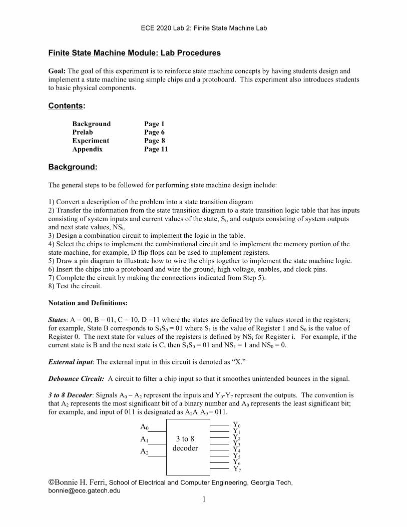
Protoboards: Protoboards (also known as breadboards) make many connections under the board in order to reduce the number of wires that you have to connect. Typically, groups of 5 holes are connected. There are also lines of groups of 5 that are all connected. See the example in Figure 1.
Integrated Chip: An integrated chip (IC) can have several gates (circuits) on it. For example, the 74HC32 IC has 4 2-input OR gates. It has 14 wire pins coming out the sides with the connections from the pins to the logic gates shown in Figure 2.
pin 1 near notch
Figure 2a: Pin Diagram to the 74HC32 Quad 2-input OR gate.
Figure 2b: Logic gates for the 74HC32 IC.
Every hole in this vertical line is connected. This is true of every vertical line.
Each horizontal group of 5 holes is connected.
Terminals Every hole in this vertical line is connected. This is true of every vertical line.
Each horizontal group of 5 holes is connected.
Terminals
Figure 1: Protoboard.
ECE 2020 Lab 2: Finite State Machine Lab
©Bonnie H. Ferri, School of Electrical and Computer Engineering, Georgia Tech, [email protected]
3
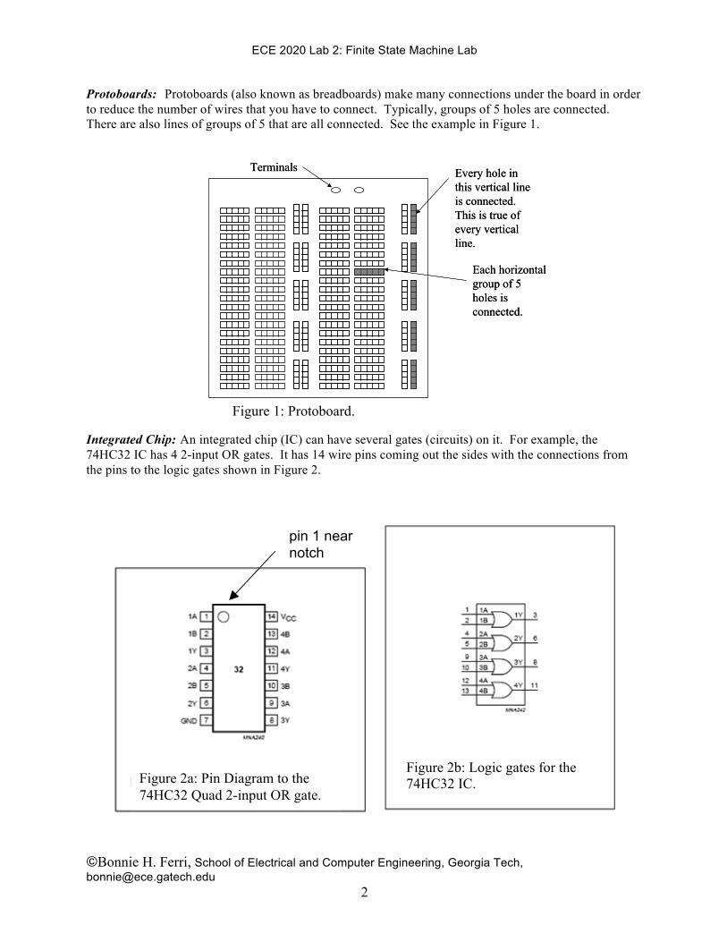
Pin Connection Diagram: A pin connection diagram shows the physical layout of the connections between components. Each component is shown along with the corresponding pin numbers for that component. The pin diagram for the logic expression F = (A OR B) OR (C OR D) is shown below. The pin numbers correspond to the pins as labeled above for the 74HC32 2-input OR chip.
Figure 3: Pin diagram for F=(A+B)+(C+D)
To build this circuit, you would need to connect a wire from pin 3 of the IC to pin 9, another wire from pin 6 to pin 10. Pins 1, 2, 4, and 5 are inputs and connect to outputs from other components while pin 8 is connected to an LED or an input to another component. Example: Consider a state machine defined by the state transition diagram in Figure 4.
A (00)
B (01)
C (10)
X = 0
X = 1
X = 1
X = 1
X = 0
X = 0 Figure 4: State Transition Diagram.
F
OR Gate 74HC32
OR Gate 74HC32
OR Gate 74HC32
A B
C D
1 2
3
5 4
6
9
10 8 F
OR Gate 74HC32
OR Gate 74HC32
OR Gate 74HC32
A B
C D
1 2
3
5 4
6
9
10 8
ECE 2020 Lab 2: Finite State Machine Lab
©Bonnie H. Ferri, School of Electrical and Computer Engineering, Georgia Tech, [email protected]
4
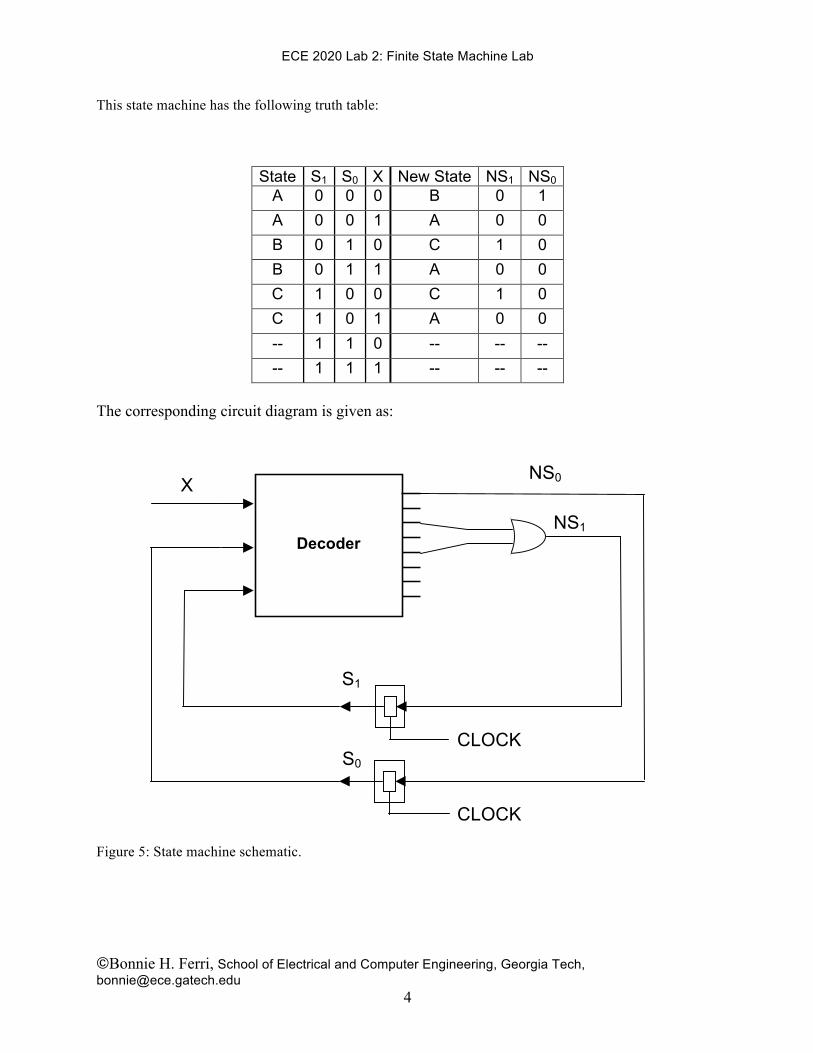
This state machine has the following truth table:
State S1 S0 X New State NS1 NS0 A 0 0 0 B 0 1 A 0 0 1 A 0 0 B 0 1 0 C 1 0 B 0 1 1 A 0 0 C 1 0 0 C 1 0 C 1 0 1 A 0 0 -- 1 1 0 -- -- -- -- 1 1 1 -- -- --
The corresponding circuit diagram is given as:
Figure 5: State machine schematic.
CLOCK
S1
S0
Decoder
CLOCK
NS1
X NS0
ECE 2020 Lab 2: Finite State Machine Lab
©Bonnie H. Ferri, School of Electrical and Computer Engineering, Georgia Tech, [email protected]
5
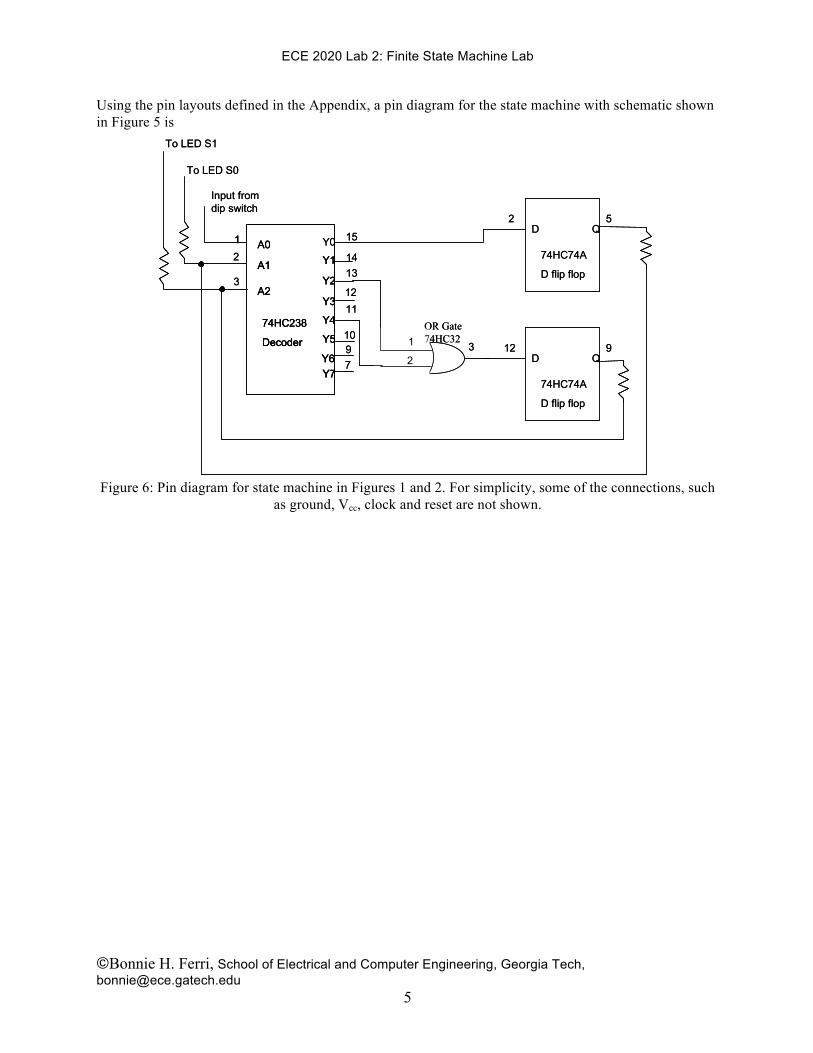
Using the pin layouts defined in the Appendix, a pin diagram for the state machine with schematic shown in Figure 5 is Figure 6: Pin diagram for state machine in Figures 1 and 2. For simplicity, some of the connections, such
as ground, Vcc, clock and reset are not shown.
15Y01
74HC238
Decoder
A0
A1
A2Y3
Y2
Y4
Y1
Y5
Y6Y7
Input from dip switch
D Q
D Q
5
9
2
12
74HC74A
D flip flop
74HC74A
D flip flop1314
910
1112
7
To LED S0
To LED S1
B
OR Gate74HC321
23
3
2
15Y01
74HC238
Decoder
A0
A1
A2Y3
Y2
Y4
Y1
Y5
Y6Y7
1
74HC238
Decoder
A0
A1
A2Y3
Y2
Y4
Y1
Y5
Y6Y7
Input from dip switch
D Q
D Q
5
9
2
12
74HC74A
D flip flop
74HC74A
D flip flop1314
910
1112
7
To LED S0
To LED S1
B
OR Gate74HC321
23
3
2
ECE 2020 Lab 2: Finite State Machine Lab
©Bonnie H. Ferri, School of Electrical and Computer Engineering, Georgia Tech, [email protected]
6
Prelab: Prior to class, do the following: • View the Tutorial on “Fundamental Concepts” • Read and thoroughly understand the Example on the previous pages. • View the video introducing the experiment:
https://www.youtube.com/watch?v=1PRok58Uumc • Complete the prelab procedure given below
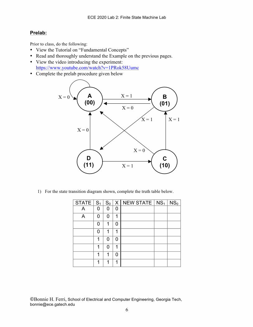
1) For the state transition diagram shown, complete the truth table below.
STATE S1 S0 X NEW STATE NS1 NS0 A 0 0 0 A 0 0 1 0 1 0 0 1 1 1 0 0 1 0 1 1 1 0 1 1 1
X = 1
X = 0
X = 1
A (00)
B (01)
X = 1
X = 0
X = 0
X = 0
X = 1 C
(10)
D (11)
ECE 2020 Lab 2: Finite State Machine Lab
©Bonnie H. Ferri, School of Electrical and Computer Engineering, Georgia Tech, [email protected]
7
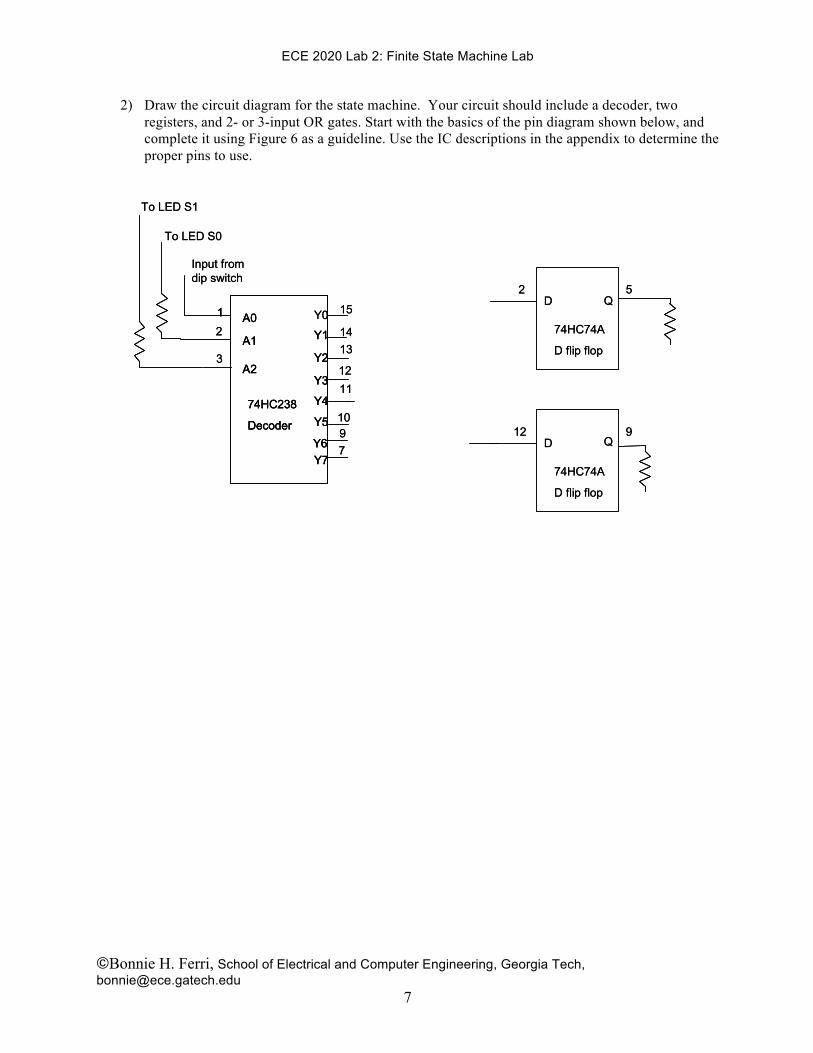
2) Draw the circuit diagram for the state machine. Your circuit should include a decoder, two registers, and 2- or 3-input OR gates. Start with the basics of the pin diagram shown below, and complete it using Figure 6 as a guideline. Use the IC descriptions in the appendix to determine the proper pins to use.
15Y01
74HC238
Decoder
A0
A1
A2Y3
Y2
Y4
Y1
Y5
Y6Y7
Input from dip switch
D Q
D Q
5
9
2
12
74HC74A
D flip flop
74HC74A
D flip flop1314
910
1112
7
To LED S0
To LED S1
3
2
15Y01
74HC238
Decoder
A0
A1
A2Y3
Y2
Y4
Y1
Y5
Y6Y7
1
74HC238
Decoder
A0
A1
A2Y3
Y2
Y4
Y1
Y5
Y6Y7
Input from dip switch
D Q
D Q
5
9
2
12
74HC74A
D flip flop
74HC74A
D flip flop1314
910
1112
7
To LED S0
To LED S1
3
2
ECE 2020 Lab 2: Finite State Machine Lab
©Bonnie H. Ferri, School of Electrical and Computer Engineering, Georgia Tech, [email protected]
8
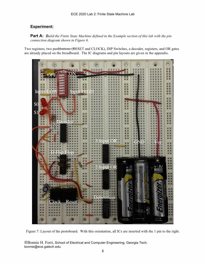
Experiment: Part A: Build the Finite State Machine defined in the Example section of this lab with the pin connection diagram shown in Figure 6.
Two registers, two pushbuttons (RESET and CLOCK), DIP Switches, a decoder, registers, and OR gates are already placed on the breadboard. The IC diagrams and pin layouts are given in the appendix.
Figure 7: Layout of the protoboard. With this orientation, all ICs are inserted with the 1 pin to the right.
ECE 2020 Lab 2: Finite State Machine Lab
©Bonnie H. Ferri, School of Electrical and Computer Engineering, Georgia Tech, [email protected]
9
The circuit is partially wired as shown in Figure 7: • The battery pack supplies high voltage (Vcc) from the red lead and the ground (GND) from the
black lead. The power routed through the uppermost dip switch, which must be turned on to power the circuits.
• The input to the state machine come from a wire connected to the right side of the bottom dip switch.
• Vcc and GND are connected to all of the ICs. • The ICs are all oriented so that the upper left pin is PIN 1 (when the board is oriented as shown
above). • The light emitting diodes (LEDs) are connected to S0 and to S1. The LEDs light when the signal
is “1”. • The reset button resets the state to State A. It is already connected to the registers. • The clock button advances the clock. The register stores the values of its input and passes the
value to its output after each time that the clock button is pushed. It is already connected to the registers.
• The resistors (small cylindrical components with stripes) are used to limit the current in some of the lines. Otherwise, the components many burn out too quickly.
• A “debounce” circuit, consisting of an additional IC and a capacitor, is connected to the clock button. A bounce is when a switch does not produce a clean signal. There may be some ripple in the signal (or perhaps a small spike) that might be interpreted by the digital logic as a second input signal, in this case, an extra clock pulse. The debounce circuit filters the signal to remove the ripple or spike.
• The decoder has the enable pins already wired.
Steps: 1) Make sure that the power is turned off of the board prior to constructing the circuit, that is, turn
off the uppermost dip switch. 2) Complete the circuit according to the PIN Connection Diagram shown in Figure 6. Use the loose
lead wires that are supplied with the kit. The color of wire is insignificant. Refer to the protoboard description to see which holes are connected within the protoboard, and refer to the appendix to see the pin numbers of the ICs.
3) Turn on the power to the circuit. 4) Now, test the State Machine to make sure it is working properly. First reset the state machine to
put it in state A. Set the DIP switch to 0 and then press the clock button. Determine the state from the LEDs and mark it in the table below. Change the input to 1 and press the clock button to see the next state value. Move the DIP switch to either the on or off position according to the table, and then press the clock button to change the state. Complete the table below to show the states corresponding to the given input sequence. Verify that this sequence follows the transitions as dictated by the state transition table in Figure 4.
State Input State Input State Input State Input State Input State Input State Input State A 0 1 1 0 0 0 1
Instructor or TA Initials: ___________
ECE 2020 Lab 2: Finite State Machine Lab
©Bonnie H. Ferri, School of Electrical and Computer Engineering, Georgia Tech, [email protected]
10
Part B: Build the Finite State Machine designed for the Prelab.
1) Turn off the power to the circuit before making any changes. 2) Remove only the wires that you added to the protoboard for Part A (do not remove the wires that
were already there) . 3) Build the circuit using the pin connection diagram that was completed for the Prelab. 4) When the state machine is complete, turn on the power. Reset the state machine to put it in state
A, and input the following sequence into the circuit. Write down the state after each step: State Input State Input State Input State Input State Input State Input State Input State A 0 1 1 1 0 1 1
Instructor or TA Initials: ___________ When finished, pull out ONLY the wires that you added to the circuit, and TURN OFF the power switch.
ECE 2020 Lab 2: Finite State Machine Lab
©Bonnie H. Ferri, School of Electrical and Computer Engineering, Georgia Tech, [email protected]
11
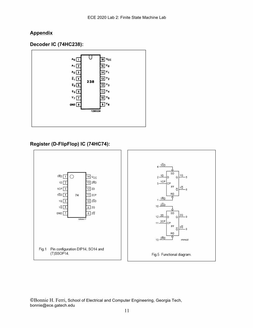
Appendix Decoder IC (74HC238):
Register (D-FlipFlop) IC (74HC74):
ECE 2020 Lab 2: Finite State Machine Lab
©Bonnie H. Ferri, School of Electrical and Computer Engineering, Georgia Tech, [email protected]
12
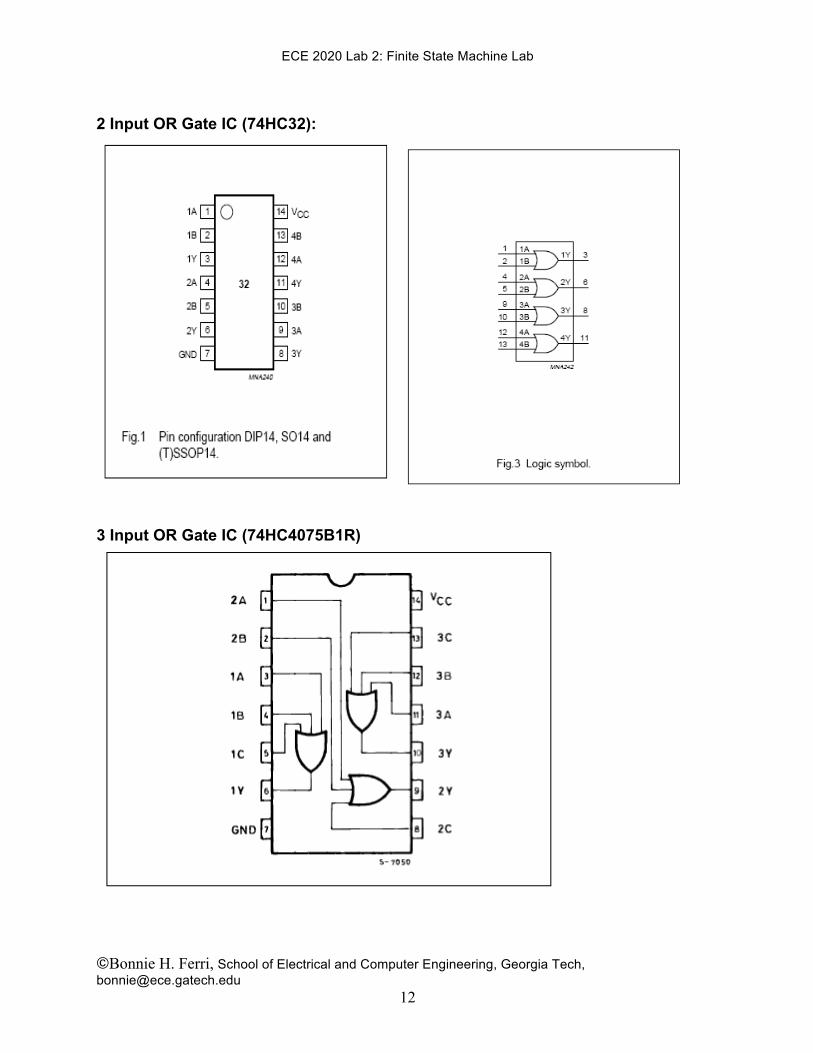
2 Input OR Gate IC (74HC32):
3 Input OR Gate IC (74HC4075B1R)