Embed Size (px)
Citation preview

Final Year Project Thesis
Implementation of Digital System Designs on LabVIEW FPGA
Student:
Anjan Mahat (09569022)
Electrical and Electronic Engineering
Supervisor:
Dr. Fearghal Morgan
Date Submitted:
03-04-2013

i
FYP-NUIG 2013
Abstract
This project describes use of LabVIEW FPGA a graphical programming language to program
FPGA. Hardware description language (HDL) is mostly used to program FPGA however this
requires good knowledge about digital system.
During EE427 course many digital system designs were designed using VHDL. The main goal
of this project is to implement designs from EE427 on sbRIO 9605 board using LabVIEW
FPGA.

ii
FYP-NUIG 2013
Statement of originality
I hereby declare that this report is my original work except where stated.
Signature: _________________ Date: _________________
(Anjan Mahat)

iii
FYP-NUIG 2013
Acknowledgement
I would like to thank my supervisor Dr. Fearghal Morgan for all his time and guidance and
support throughout this project. I also like to thank my co- supervisor Dr. Martin Glavin for his
time and support for this project.
And also many thanks technician Myles Meehan and Martin Burke for all the help on getting the
resources needed for this project.

iv
FYP-NUIG 2013
Table of contents
Abstract ....................................................................................................................................................... i
Statement of originality .............................................................................................................................. ii
Acknowledgement ......................................................................................................................................iii
Table of contents ........................................................................................................................................ iv
List of Figures .............................................................................................................................................. vi
List of Acronyms ........................................................................................................................................ vii
Introduction ............................................................................................................................................... 1
1.1 Introduction to project...................................................................................................................... 1
1.2 Project goal ....................................................................................................................................... 2
1.3 Structure of the report ...................................................................................................................... 3
Chapter 2: LabVIEW and LabVIEW FPGA ................................................................................................... 4
2.1 LabVIEW ............................................................................................................................................ 4
2.2 LabVIEW FPGA .................................................................................................................................. 4
Frequently used useful functional graphical blocks ........................................................................ 4
2.2.1 LabVIEW FPGA compilation process .......................................................................................... 5
2.2.2 Communicating with host PC and FPGA target .......................................................................... 5
Interactive Front panel communication .......................................................................................... 6
Programmatic FPGA interface communication ............................................................................... 7
2.2.3 LabVIEW FPGA communicating with sbRIO 9605 ....................................................................... 8
2.2.4 Testing on emulator ................................................................................................................... 8
2.2.5 Xilinx CORE Generator ................................................................................................................ 8
Chapter 3: Applications .............................................................................................................................. 9
3.1 Blink Led ............................................................................................................................................ 9
3.1.1 Implementation in LabVIEW FPGA ............................................................................................. 9
3.1.2 Implementation process ........................................................................................................ 9
3.2 8-bit Up/down counter ................................................................................................................... 10
3.2.1 Implementation in LabVIEW FPGA ........................................................................................... 10
3.3 singleShot........................................................................................................................................ 11
3.3.1 Implementation in LabVIEW FPGA ........................................................................................... 11
3.3.2 Implementation process ...................................................................................................... 12
3.4 Control register block ...................................................................................................................... 13
3.4.1 Implementation in LabVIEW FPGA ........................................................................................... 13
3.4.2 Implementation process ...................................................................................................... 14
3.5 Host control register block write/read ............................................................................................ 16
3.5.1 Implementation in LabVIEW FPGA ........................................................................................... 17

v
FYP-NUIG 2013
3.5.2 Implementation process ...................................................................................................... 17
Chapter 4: Results .................................................................................................................................... 19
4.1 Up/down Counter ........................................................................................................................... 19
4.2 Singleshot........................................................................................................................................ 19
4.3 Control Register Block ..................................................................................................................... 20
4.4 Host Control Register Block............................................................................................................. 21
Chapter 5: Discussion and Conclusion ..................................................................................................... 22
5.1 Conclusion ....................................................................................................................................... 22
5.2 Future work..................................................................................................................................... 22
Reference ................................................................................................................................................. 23
Appendix .................................................................................................................................................. 24
A 1 Quick start guide ............................................................................................................................. 24
A1.1 Configure the board on MAX .................................................................................................... 24
A1.2 Create Blink LED project ........................................................................................................... 25
A 2 Enumerated State machine ............................................................................................................ 29

vi
FYP-NUIG 2013
List of Figures
Figure 1-1: Design example ............................................................................................................ 1
Figure 1-2: System Diagram ........................................................................................................... 2
Figure 2-1: While Loop .................................................................................................................. 4
Figure 2-2: Case structure ............................................................................................................... 5
Figure 2-3: Feedback Node ............................................................................................................. 5
Figure 2-4: Different types of Virtual Instrument (VI) ................................................................... 6
Figure 2-5: Front Panel communication ......................................................................................... 7
Figure 2-6: 9605 board diagram ..................................................................................................... 8
Figure 3-1: Counter functional partition ....................................................................................... 10
Figure 3-2: Counter in LabVIEW ................................................................................................. 10
Figure 3-3: singleShot FSM & functional partition ...................................................................... 11
Figure 3-4 : singleShot in LabVIEW ............................................................................................ 12
Figure 3-5 : Control Register Block.............................................................................................. 13
Figure 3-6: Control Register Block in LabVIEW ......................................................................... 14
Figure 3-6-1 : 3to8 decoder in LabVIEW ..................................................................................... 14
Figure 3-7 : Host control read/write.............................................................................................. 16
Figure 3-8 : Host control read/write FSM..................................................................................... 17
Figure 3-9 : Host control read/write in LabVIEW ........................................................................ 18
Figure 3-9-1 : Host write state ...................................................................................................... 18
Figure 4-1: Counter Front Panel ................................................................................................... 19
Figure 4-2: singleShot Front Panel ............................................................................................... 19
Figure 4-3-1: Control Register Front Panel (a) ............................................................................. 20
Figure 4-3-2 : Control Register Block Front Panel (b) ................................................................. 20
Figure 4-4-1: Host Control read/write Front Panel (b) ................................................................. 21
Figure 4-4-2: Host Control read/write Front Panel (a) ................................................................. 21
vii
FYP-NUIG 2013
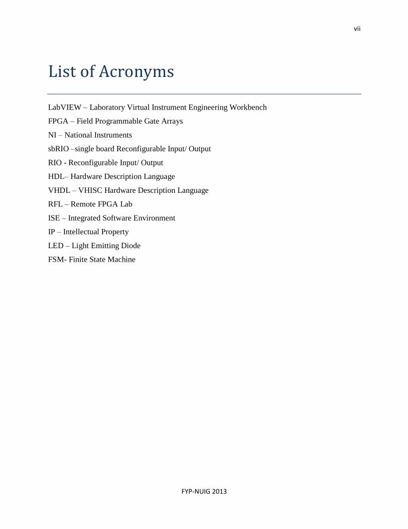
List of Acronyms
LabVIEW – Laboratory Virtual Instrument Engineering Workbench
FPGA – Field Programmable Gate Arrays
NI – National Instruments
sbRIO –single board Reconfigurable Input/ Output
RIO - Reconfigurable Input/ Output
HDL– Hardware Description Language
VHDL – VHISC Hardware Description Language
RFL – Remote FPGA Lab
ISE – Integrated Software Environment
IP – Intellectual Property
LED – Light Emitting Diode
FSM- Finite State Machine

1
FYP-NUIG 2013
Introduction
1.1 Introduction to project
FPGA is a reconfigurable system on a chip that consists of thousand of unconnected logic blocks
with programmable interconnection. FPGA can be programmed to do almost any digital function
and HDL is mainly used to program FPGA. However using HDL to program FPGA requires
high level knowledge about digital systems.
Throughout Digital system course EE427 [1] number of digital system design were implemented
on FPGA. Designs were programmed using VHDL and the bitstream files were generated and
uploaded to NUIGs Remote FPGA Lab [2] for user interaction.
LabVIEW is graphical programming language and LabVIEW FPGA is extension to LabVIEW’s
graphical platform to target FPGA. Programming FPGA with LabVIEW’s graphical platform
doesn’t require having high level of HDL knowledge [3]. It also has interactive front panel for
user interaction.
The aim of this project is to program application designed during EE427 on LabVIEW FPGA
and implement them on NI sbRIO 9605 board.
An example of an application that has been implemented is shown in (Fig 1-1).It shows the
block diagram (LabVIEW code) and front panel (user interaction) for control register block.
Every application designed in LabVIEW has a block diagram and a front panel. Front panel can
have real world instruments e.g. Switches, LEDs for user interaction
Figure 1-1: Design example

2
FYP-NUIG 2013
The NI sbRIO 9605 board used for this project has embedded Microprocessor, Spartan-6 FPGA
and specialized I/O pins. The connection between host PC and the board is achieved using
Ethernet crossover cable as shown in (fig 1-2)
Figure 1-2: System Diagram
1.2 Project goal
This project begins with learning and commissioning LabVIEW and LabVIEW FPGA with
sbRIO 9605 board. The first goal of this project is to learn and understand the structure on
programming in LabVIEW FPGA and commission NI sbRIO 9605 board
After initiate with LabVIEW and sbRIO 9605 the next goal is to develop and implement series of
digital design from EE427 on 9605 board using LabVIEW FPGA
Produce quick start guide for LabVIEW FPGA. Quick start guide should detail all material
needed to start with LabVIEW FPGA and sbRIO 9605 board and steps guide to create a simple
project
This project also looks at HDL strategies with graphical approach on programming FPGA.
During the EE427 course digital designs were implemented using VHDL text based code and for

3
FYP-NUIG 2013
this project these design will be implemented using LabVIEW FPGA graphical programming
language.
1.3 Structure of the report
This report is divided into chapters:
Chapter 2: LabVIEW and LabVIEW FPGA: This chapter gives background on LabVIEW
and LabVIEW FPGA and also provide details on how graphical programming language
LabVIEW FPGA works on targeting FPGA. This chapter will also demonstrate the learning of
LabVIEW FPGA during this project.
Chapter3: Applications: This chapter outlines different designs that were implemented on
sbRIO 9605 board using LabVIEW FPGA. This chapter gives function of each application that
has developed and implemented on LabVIEW.
Chapter4: Result: This chapter looks front panel and functionality of each of the application
explained in chapter 4
Chapter5: Discussion and Conclusion: This chapter discusses about using LabVIEW FPGA a
graphical programming language to program FPGA and suggest future work can be done with
this project
Appendix: This section provides start guide for future user for using LabVIEW FPGA with
sbRIO 9605. It outlines all the software and hardware needed and steps on creating a project to
blink a LED on the board. This section also provides steps on creating state machine with
enumerated data.

4
FYP-NUIG 2013
Chapter 2: LabVIEW and LabVIEW FPGA
This chapter gives background on LabVIEW and LabVIEW FPGA and what was learnt about
LabVIEW FPGA. This chapter will also describe how LabVIEW FPGA works with the FPGA
target and useful functions in LabVIEW.
2.1 LabVIEW
LabVIEW produced by National Instruments is visual programming language that allows
creating program with graphics instead of text based code.
LabVIEW code/ programs is called Virtual Instrument or VI and it can have copy of real world
instruments e.g switches and LED on its virtual workbench
On creation of new VI two major windows are opened:
Block diagram where graphical code is built
Front panel where the virtual instrument (e.g. Waveform, switches) are created and
displayed for user interaction.
LabVIEW codes are built by wiring the nodes of functional graphical blocks together. The node
of functional graphical blocks only executes its function only after it has received data from
previous node
2.2 LabVIEW FPGA
LabVIEW FPGA is extension to LabVIEW to target FPGA on NI reconfigurable I/O boards.
Codes are built with same process by wiring nodes together.
Frequently used useful functional graphical blocks
While loop (fig 2-1) is frequently used when designing with LabVIEW
FPGA. The while loop continuously iterates graphical code inside it. The loop
Figure 2-1: While Loop
5
FYP-NUIG 2013
is connected to 40MHz global clock and iterates at 25ns. Each iteration of the loop corresponds
to one clock cycle (tick). Loop iteration can be controlled by using loop timer. e.g if loop time is
set to 500ms then the loop will iterate once then wait for 500ms for next iteration. If there is no
while loop around the block diagram code then the code will only run once.
The Case structure (fig 2-2) is similar to if <....>then<....>else statement in
traditional language (e.g.VHDL). During this project it mainly used for
implementation of state machine and decoder. The value connected to the
selector terminal of the case structure controls the cases/states.
Feedback node (fig 2-3) in LabVIEW FPGA is used to store data from one loop
iteration to the next. In this project the feedback node is used as D type Flip-Flop.
2.2.1 LabVIEW FPGA compilation process
To generate a bitstream configuration file from users block diagram, LabVIEW FPGA uses
Xilinx ISE compiler. In background an intermediate file is created for that block diagram before
it could be compiled using Xilinx ISE compiler. This way users block diagram is converted into
text based VHDL code so the Xilinx compiler can understand. After the bitstream configuration
file is generated, LabVIEW downloads the file to the FPGA target.
2.2.2 Communicating with host PC and FPGA target
In LabVIEW FPGA there are different types of VI that can be created to run on different system
as shown (fig 2-4)
FPGA VI created by selecting FPGA Target to run on FPGA
Figure 2-2: Case structure
Figure 2-3: Feedback Node

6
FYP-NUIG 2013
Host VI could be
Real time VI created by selecting RT Single-Board RIO to run on Real-time processor
Windows VI created by selecting my computer to run on windows
`
Figure 2-4: Different types of Virtual instrument (VI)
There are two ways of communicating with FPGA target
Interactive Front panel communication
This communication can be achieved if the VI is created targeting FPGA and the VI is called
FPGA VI. In this communication the compiled FPGA VI’s block diagram executes on the FPGA
target while FPGA VI’s front panel is displayed on host computer as shown in (fig 2-5). Front
panel on host computer communicates with block diagram running on FPGA target as often as
possible to exchange state of control and indicators.
Host VI
FPGA VI

7
FYP-NUIG 2013
Figure 2-5: Front Panel communication
The front panel data shared during interactive front panel communication is not deterministic. [4]
Programmatic FPGA interface communication
This communication requires creating a host VI. The host VI runs on the host computer and
communicates with the FPGA VI running on the FPGA target. The host VI can be either targeted
to run on real time processor or windows.
Host VI should consists [5] of
Open FPGA reference VI that loads selected FPGA VI or bit file to the FPGA
Read/write control node connects to the FPGA front panel
Close FPGA VI reference closes the connection to the FPGA and free up reference VI
Host VI is used if there is needed to perform operation that are not available on FPGA or wanted
to do more data processing than you can fit on the FPGA.
8
FYP-NUIG 2013
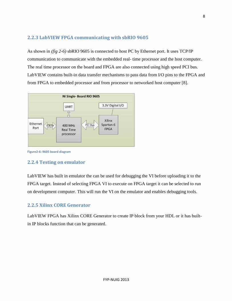
2.2.3 LabVIEW FPGA communicating with sbRIO 9605
As shown in (fig 2-6) sbRIO 9605 is connected to host PC by Ethernet port. It uses TCP/IP
communication to communicate with the embedded real- time processor and the host computer.
The real time processor on the board and FPGA are also connected using high speed PCI bus.
LabVIEW contains built-in data transfer mechanisms to pass data from I/O pins to the FPGA and
from FPGA to embedded processor and from processor to networked host computer [8].
Figure2-6: 9605 board diagram
2.2.4 Testing on emulator
LabVIEW has built in emulator the can be used for debugging the VI before uploading it to the
FPGA target. Instead of selecting FPGA VI to execute on FPGA target it can be selected to run
on development computer. This will run the VI on the emulator and enables debugging tools.
2.2.5 Xilinx CORE Generator
LabVIEW FPGA has Xilinx CORE Generator to create IP block from your HDL or it has built-
in IP blocks function that can be generated.

9
FYP-NUIG 2013
Chapter 3: Applications
This chapter describes different digital system designs that were implemented on sbRIO 9605
using LabVIEW FPGA. It details function of each application and implementation on LabVIEW.
3.1 Blink Led
The first application built to test the board’s configuration and familiarise on programming with
LabVIEW FPGA. This application causes onboard LED to blink every few seconds. Quick
tutorial guide was prepared for this see appendix A 1.2
3.1.1 Implementation in LabVIEW FPGA
The onboard I/O FPGA LED is placed inside a while loop and connected to shift register.
Indicator is created for the virtual led to display on the front panel. While loop is set to executes
every 500ms causing the led to blink both on Front Panel and the 9605 board.
3.1.2 Implementation process
See appendix A 1.2
10
FYP-NUIG 2013
3.2 8-bit Up/down counter
8 bit up/ down counter with count enable (ce) and synchronous load (ld). The counter starts to
count either up/down if count enable signal is set to high. The direction of the count can be
selected by selection input (uD), if set to high it starts counting up and if set to low it counts
down. Also 8- bit value can be loaded to counter to start the count from the loaded value.
Figure 3-1: Counter functional partition
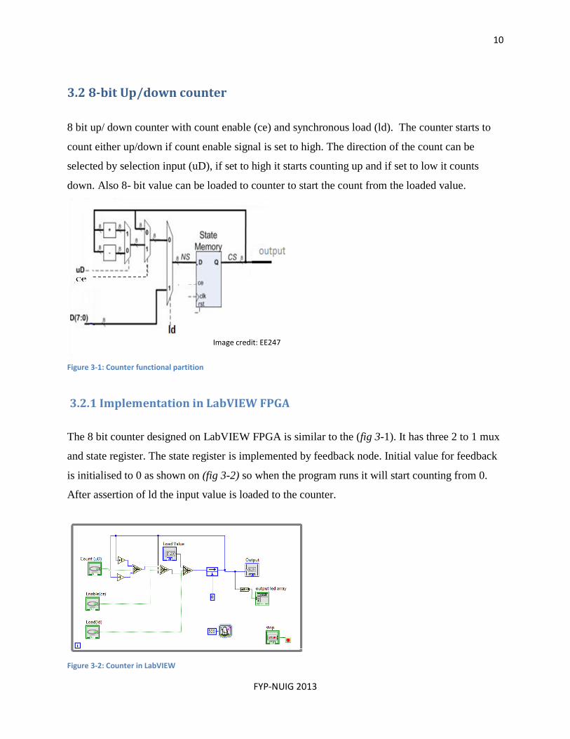
3.2.1 Implementation in LabVIEW FPGA
The 8 bit counter designed on LabVIEW FPGA is similar to the (fig 3-1). It has three 2 to 1 mux
and state register. The state register is implemented by feedback node. Initial value for feedback
is initialised to 0 as shown on (fig 3-2) so when the program runs it will start counting from 0.
After assertion of ld the input value is loaded to the counter.
Figure 3-2: Counter in LabVIEW
Image credit: EE247

11
FYP-NUIG 2013
3.3 singleShot
singleShot is rising edge detector for a switch. The rising edge of switch is detected using a state
machine described by the flow chart in (fig 3-3). As shown on flow chart it waits for switch to go
high (waitFor1). As the switch goes high it will turn on the LED and move to the next state
(waitFor0). In the next state LED is turned off and it waits for switch to go low. Hence LED is
turned on only on rising edge of the switch input
3.3.1 Implementation in LabVIEW FPGA
The state machine is implemented using case statement. Case statement has two cases as shown
in (fig 3-4) True (waitfor1) and False (waitFor0). Input of switch changes the states .Feedback
node acts as state register.
Figure 3-3: singleShot FSM & functional partition

12
FYP-NUIG 2013
3.3.2 Implementation process
To control the state from input of a switch it
is passed through feedback node and
connected to the selector terminal of the
case structure. Switch high selects True
state and low selects False state.
To detect the rising edge of the switch it is
connected to AND gate and also the
converted value of the state is connected to
the AND gate. This way The LED only
turns on if the last state was false (waitfo0)
and the switch is high.
The output of the AND gate is high thus
LED on, only if the last state is false
(switch low) since it gets converted before
fed to the AND gate and if switch is high.
The loop timer is set to execute every 500ms so when LED turns on it can be seen. This is
because the while loop is connected to the global clock 40 MHz which executes at 25ns.
Figure 3-4: singleShot in LabVIEW

13
FYP-NUIG 2013
3.4 Control register block
The function of control register block (fig 3-5) is to write/read 8 bit data to/from 8 byte wide
registers. On write enable signal (enWr) being high it stores the 8 bit input data (ctrlRegIn) to the
selected register. When write enable signal is low it will read the stored data from the selected
register. The register is selected by 3 bit input (ctrlRegAdd). 3 to 8 decoder is used to decode 3
bit input to select 8 registers.
Figure 3-5: Control Register Block
3.4.1 Implementation in LabVIEW FPGA
Feedback node stores data from one loop iteration to next. Therefore to store data feedback node
is used as register. As shown in (fig 3-6) 8 bit ctrlRegIn is connected to all 8 mux and output of
mux are connected directly to inputs of the feedback nodes.3 bit Address input is decoded and
connected to selector terminal of each of the eight mux. If the selector of the mux is high then
ctrlRegIn is passed to the feedback node. Feedback node has enable terminal, which if set to
false it keeps outputting the last stored value and if set to true it stores the new value. Therefore
write enable signal is connected to enable terminal of feedback node
Image credit: remote FPGA Lab

14
FYP-NUIG 2013
Figure 3-6: Control Register Block in LabVIEW
Figure 3-6-1 : 3to8 decoder in LabVIEW
3.4.2 Implementation process
To have 8 bit input fixed array of size 8 is created and connected to the ‘1’ terminals of the mux.
The selector of mux are connected from output of 3to 8 decoder
3 to 8 decoder is built by using case statement see (fig 3 -6-1). 3 bit input is concatenated and
converted from array to number and is connected selector terminal of the case statement. This
way 3 bit input controls the states and allows having many cases. Eight different cases were
created and 8 bit fixed array inside each cases was connected as output. For combination of each
3 bit input there is 8 bit output with just 1 bit high. The output is unbundled so each bits of the
array has connection and can be connected to selector of the eight mux

15
FYP-NUIG 2013
The output of each feedback node is created as an indicator to have output ctrlReg (7:0) (7:0)
arrays of 8 bytes. The array of 8 bytes is displayed on the front panel by LEDs.
To have selected register output (ctrlRegOut), output of each of the feedback node is connected
as inputs to a case structure as shown (fig 3-6). Same as in for 3to8 decoder the 3 bit address
input is concatenated and converted to number and connected to selector terminal of the case
structure. Eight different cases are created and for each case a different feedback node output is
connected as output for the case structure.

16
FYP-NUIG 2013
3.5 Host control register block write/read
The host control register block (fig 3-7) sends command to either write or read to/from 8 byte
wide control register block. It uses a state machine (fig 3-8) to decode the 4 bit command byte to
determine either to perform write or read. State machine is activated if signal goDesign is high.
DesignDone signal indicates read or write cycle is done. regCtrlRegInfo signal activates
ctrlRegAdd. enCtrlRegWr activates write enable signal in control register block.
On write state it waits for assertion of rxDatValid signal to indicate that input data(rxDat) is
valid. Asserts write enable singnal and writes the input data (rxDat) to the control register block
addrresed by ctrlregAdd
On the read state txDatValid indicates that addressed register data is on ctrlRegOut and waits for
assertion of txDatAck handshake signal from host to indicate ctrlRegOut has been taken by host.
Figure 3-7: Host control read/write
Image credit: EE247

17
FYP-NUIG 2013
Figure 3-8: Host control read/write FSM
3.5.1 Implementation in LabVIEW FPGA
State machine is implemented using case structure. Enumerated data type is used for case
structure to have suitable names for each state. Appendix A2 describes on creating enumerated
case structure. Previously created Control Register Block VI is used as a sub VI. rxDat is
connected to the control register block
3.5.2 Implementation process
As shown in (fig 3-9) to decode 4 bit command byte it is concatenated and converted to number.
The converted 4 bit command is compared with constant value 3 for input of 1100 (write) and 11
for input of 1101(read) state. The results of the compared values are connected to different AND
gates with goDesign input. This set output of AND gates high if the compared value and
goDesign both are high. The output of the AND gates are connected to different selector
Image credit: EE247

18
FYP-NUIG 2013
terminals of 2 to 1 mux. Each terminal of mux are connected with different state which will be
selected depending from the output of the AND gates
In write state rxDatValid is connected to selector terminal of the mux as shown in (fig 3-9-1). If
the rxDatValid is high then it goes to next state (waitforRxDatValid0) else stays on that state. In
waitforRxDatValid0 state where it waits for rxDatValid to go low, it compares if the rxDatValid
is false (low), if so then moves to next state w1. In w1 state enCtrlRegWr is set to true and next
state is assigned chkTask (default state) and write cycle is complete. Same principle applied to
the read state where it waits for assertion of txDatAck.
Figure 3-9: Host control read/write in LabVIEW
Figure 3-9-1: Host write state

19
FYP-NUIG 2013
Chapter 4: Results
This chapter looks at the front panel functionality of the different applications that were
implemented on LabVIEW FPGA and 9605 board.
4.1 Up/down Counter
Counter starts counting from initial value of 0 if the enable (ce) is high. Assertion of load (ld)
loads the value to the counter. As shown in (fig 4-1) value of 99 is loaded and count (uD) is low
so the count starts downwards and when the uD is high the count starts upwards.
Figure 4-1: Counter Front Panel
4.2 Singleshot
As shown in (fig 4-2) The LED turned on and off even if the switch is still on. Hence the LED is
turned on only on the rising edge of the switch
Figure 4-2: singleShot Front Panel

20
FYP-NUIG 2013
4.3 Control Register Block
8 bit data is stored on byte wide register are displayed by LEDs. On assertion of write enable
signal (enwr), input data is stored into byte wide register selected by CtrlRegAdd. On write
signal being low meaning read CtrlregOut displayed selected registers stored value. As shown in
(fig4-3-1) enWr is high and CtrlRegIn is written to reg2 (CtrlRegAdd =010). Next (fig 4-3 -2))
enWr is low and the value stored on reg1 (001) is outputted on CtrlregOut
Figure 4-3-1: Control Register Front Panel (a)
Figure 4-3-2: Control Register Block Front Panel (b)
8 Byte wide registers implemented using feedback nodes
Write
Read

21
FYP-NUIG 2013
4.4 Host Control Register Block
Switches act as control and LED as indicators. Front panel also displayed the current states
(IO_state) and the number value of converted 4 bit Command input. To write rxDat to control
register it waits until the rxDatVAlid is asserted. As shown in (fig 4-4-1) command is 1100 and
corresponding number is 3 and IO_state shows current state waiting for rxDatValid to go low.
rxDat is written by enabling write enable signal to control register block after assertion of
rxDatValid. To read as shown in (fig 4-4-2) the command is 1101 and after the assertion of
txDatAck the value of reg0 (ctrlRegAdd =000) is outputted on ctrlRegOut.
Figure 4-4-2: Host Control read/write Front Panel (b)
Implemented by Control register block
Write
Read
Figure 4-4-1: Host Control read/write Front Panel (a)

22
FYP-NUIG 2013
Chapter 5: Discussion and Conclusion
After working in this project with no previous knowledge on LabVIEW it has helped to gain
knowledge on LabVIEW. Also working on this project has helped to further my knowledge on
digital system designs
5.1 Conclusion
LabVIEW and HDL both have steep learning curves. However if one is proficient in
programming on LabVIEW transition from LabVIEW to LabVIEW FPGA is not a steep learning
curve.
The advantages of using LabVIEW FPGA to program FPGA are that it doesn’t require having
knowledge of HDL or board – level hardware design. It can have real world instrument in its
virtual workbench e.g. switches, LED for user interaction. And the hardware built to target
LabVIEW FPGA is built by combining Microprocessor, FPGA and specialized I/O for advanced
control and monitoring.
LabVIEW also has some disadvantages on programming FPGA. Some of the LabVIEW FPGA
interfaces are abstract. Not all the FPGA boards can be targeted to the LabVIEW FPGA.
5.2 Future work
The future work for this project will be developing a higher level application in LabVIEW
FPGA. To develop a host VI to communicate with FPGA VI to perform advanced processing
(e.g. image, audio)

23
FYP-NUIG 2013
Reference
[1] [Dr.Fearghal Morgan, EE427 assignment (14 September 2012)]
http://fmorgan.starlightlabs.com/EE427/AsgnRelease/
[2] [NUIG, Remote FPGA Lab]
http://remotefpga.com/home/
[3] [NI.com, Graphical system design, (4th quarter 2011) pg 4-7]
http://www.ni.com/pdf/newsletters/us/INL_Q4_2011_IA.pdf
[4] [NI.com, Interactive front panel communication (June 2012)]
http://zone.ni.com/reference/en-XX/help/371599H-01/lvfpgaconcepts/ifp_comm/
[5] [edoering , Device interface with transparent FPGA, (12 August 2009 )]
https://decibel.ni.com/content/docs/DOC-6261
[6] [edoering, digsys -00: Digital Circuits and System with LabVIEW FPGA (17 September 2009)]
https://decibel.ni.com/content/docs/DOC-6825
[7] [NI.com, Operating instruction and specification NI sbRIO 9605 (September 2011)]
http://www.ni.com/pdf/manuals/373378a.pdf
[8] [NI Single-Board RIO Embedded Control and Acquisition (12 October 2012)]
http://www.ni.com/white-paper/7441/en
[9] [Storing data on FPGA target, June 2012]
http://zone.ni.com/reference/en-XX/help/371599H-01/lvfpgaconcepts/fpga_storing_data/
[10] [edoering, digsys-03 Audio Meter (24 July 2009)]
https://decibel.ni.com/content/docs/DOC-5827
[11] [Chris Washington, edge detection on digital signal, (4 October 2012)]
https://decibel.ni.com/content/docs/DOC-1047
[12] [Interfacing a LabVIEW Real-time Via TCP/IP, (05 May 2012)]
http://www.ni.com/white-paper/3524/en
[13] [LabVIEW 2012 FPGA Module Help, (June 2012)]
http://zone.ni.com/reference/en-XX/help/371599H-01/
[14] [Introduction to Debugging FPGA VIs on the Host, (June 2012)]
http://zone.ni.com/reference/en-XX/help/371599H-01/lvfpgahelp/running_fpga_vi_on_emulator/
[15] [Increase IP Reuse with the Xilinx CORE Generator IP Palette (26 0ctober 2011)]
http://www.ni.com/white-paper/12918/en
(All links accessed on 1-4-2013)

24
FYP-NUIG 2013
Appendix
A 1 Quick start guide
Quick start Guide for LabVIEW FPGA and sbRIO 9605 board
Software needed
LabVIEW core software (includes Measurement & Automation Explorer)
LabVIEW FPGA module (includes Xilinx tools)
LabVIEW Real-Time module
NI RIO driver
Approx download time (4-5 hours)
Hardware needed
NI sbRIO 9605 board
9-30v power supply
Ethernet crossover cable
A1.1 Configure the board on MAX Before the board can be targeted on LabVIEW FPGA it has to be first configured using Measurement & Automation Explorer (MAX)
1. Connect the board to power supply and connect the board to pc using Ethernet crossover cable 2. Open (MAX) and click on remote system. Name of device is displayed if connected properly.
Help are available on right hand side of the window
3. Right click on software to add or remove software to the board.
4. When the software is installed device can be selected as target in LabVIEW.

25
FYP-NUIG 2013
A1.2 Create Blink LED project 5. Open new project and to select target by right clicking on project >> New >> Targets and
Devices
6. Click on real time single-board RIO to select the target, if connected correctly device is displayed
7. When target is selected, FPGA and chassis in the windows are displayed
8. To open the VI right click on FPGA Target >> New >> VI. This opens blank Front Panel and Block
Diagram

26
FYP-NUIG 2013
9. Start to design program on Block diagram. Insert while loop by Right click on block diagram window >> structure >> while loop
10. Add Boolean constant outside and inside the while loop. Right click>> Boolean>>False constant. Connect outside constant to while loop and inside constant to red loop condition. On loop tunnel Right click>> Replace with shift register
11. Add NOT gate inside the while loop. And connect across the while loop

27
FYP-NUIG 2013
12. Drag and drop FPGA Led from onboard IO from the project explorer inside the while loop and
connect it after output of NOT connection
13. Right click on the connection >> create>>indicator. This creates indicator which can be seen in
the Front Panel. You can resize it by dragging
14. To insert loop timer Right click>> Timing>> Loop Timer. Put this inside the while loop. Select counter units to mSec

28
FYP-NUIG 2013
15. Add value for time. Right Click >> Numeric >> numeric counter. Or right click on loop timer and select create>> constant. Type 500 inside the counter and connect to loop timer
16. Click on the run button, it should start compiling using Compile worker. When the compile is
successful the led in Front Panel and the userf1 LED on NI sbRIO 9605 board should blink every 500ms. The while loop iterates every 500ms causing the led to blink. Xilinx log report can be viewed while compiling.

29
FYP-NUIG 2013
A 2 Enumerated State machine
Steps to create enumerated type case statement (state machine)
Create enumerated data type 1. Right click on front panel >> Ring & Enum >> Enum. This will enter enum data type field on the
front panel
2. On Enum field Right click >> edit Item..
3. window below should open, fill this with each state for state machine and assign value as o being default state and click ok

30
FYP-NUIG 2013
4. On the block diagram enum node is displayed. Change enum state to constant by right click on it >> change to constant. It should display as below and when clicked down arrow on constant it shows the list of different states. You can copy and paste to create many of these constant
Create state machine 5. Add case structure right click on the block diagram >> structures>> case structure
6. Add feedback node for state register right click >> structures>> Feedback Node. Change the
direction by right click on the feedback node>> change direction.
7. Connect feedback node, enumerated constant and selector terminal of case structure as below.
Select the default state to connect to initial terminal of feedback node.

31
FYP-NUIG 2013
8. To add a switch right click >> Boolean palette >> false constant and right click on the constant >> change to control This will act as switch and displays on front panel for user control. Connect the switch to input of case statement
9. Inside a case waitFor1 add equal and 2to 1 mux, right click >> Comparison Palette >> Equal and >>
2 to 1 mux(Select). Also add Boolean palette>> true Boolean constant and connect as follows. Connect output of equal to the output of the case structure and Right click on the tunnel >>create indicator. This creates LED on front panel
10. Move to case waitFor0. Have the same components as for waitFor0 case but change true boolean
constant to false and don’t connected the output of equal to output of case statement instead connect false Boolean constant.

32
FYP-NUIG 2013
11. Insert a while loop around the diagram. At loop condition (red dot) right click >> create control. This creates stop button for while loop. Add timing palette >> loop timer >> and select counter units to msec. Right click on loop timer>> create constant. Insert 1000, this causes while loop to iterate every 1 sec.
Front panel should display as below.