Embed Size (px)
Citation preview
SYLLABUS�(With effect from 2013-2014)�Out Come Based Education
����������� ���������������������������������� �������
V and VI Semester Bachelor Degree
in Electronics and Communication Engineering
P.E.S. College of Engineering Mandya - 571 401, Karnataka
(An Autonomous Institution ����������� VTU, Belagavi) Grant -in- Aid Institution
(Government of Karnataka) Accredited by NBA, New Delhi
Approved by AICTE, New Delhi. �
����������� ����������������������������������� !"���
#��$��������%&'�(��)*����+, ���-�����.�����&/0�Ph : 08232- 220043, Fax : 08232 – 222075,Web : www.pescemandya.org
�����
PrefacePES College of Engineering, Mandya, started in the year 1962, has become autonomous
in the academic year 2008-09. Since, then it has been doing the academic and examination activities successfully. The college is running eight undergraduate and eight Postgraduate programs. It consists of six M.Tech programs, which are affiliated to VTU. Other postgraduate programs are MBA and MCA.
India has recently become a Permanent Member by signing the Washington Accord. The accord was signed by the National Board of Accreditation (NBA) on behalf of India on 13th June 2014. It enables not only the mobility of our degree globally but also establishes equivalence to our degrees with that of the member nations such as Taiwan, Hong Kong, Ireland, Korea, Malaysia, New Zealand, Russia, Singapore, South Africa, Turkey, Australia, Canada and Japan. Among other signatories to the international agreement are the US and the UK. Implementation of Outcome Based Education (OBE), has been the core issue for enabling the equivalence and of Indian degrees and their mobility across the countries.
Our Higher Educational Institution has adopted the semester structure with OBE scheme and grading system.
The credit based OBE semester system provides flexibility in designing curriculum and assigning credits based on the course content and hours of teaching.
The OBE, emphasize setting clear standards for observable, measurable outcomes of programs in stages. There lies a shift in thinking, teaching and learning processes moving towards Students Centric from Teacher Centric education. OBE standards focus on mathematics, language, science, attitudes, social skills & moral values.
The key features which may be used to judge, if a system has implemented an outcome based education system is mainly Standard based assessments that determines whether students have achieved the stated standard. Assessments may take any form, so long as the process actually measure whether the student knows the required information or can perform the required task. Outcome based education is a commitment that all students of all groups will ultimately reach the same minimum standards. Outcome Based Education is a method or means which begins with the end in mind and constantly emphasizes continuous improvement.
In order to increase the Industry/Corporate readiness, many Soft Skills and Personality Development modules have been added to the existing curriculum of 2013-14.Industry Interactions have been made compulsory to enhance the field experience. In order to enhance creativity and innovation Mini Project is included in all undergraduate programs.
Dr.H.V.RAVINDRA Dean (Academic) Professor, Dept. of Mechanical Engg.
B.DINESH PRABHU Deputy Dean (Academic)
Associate Professor, Dept. of Automobile Engg.
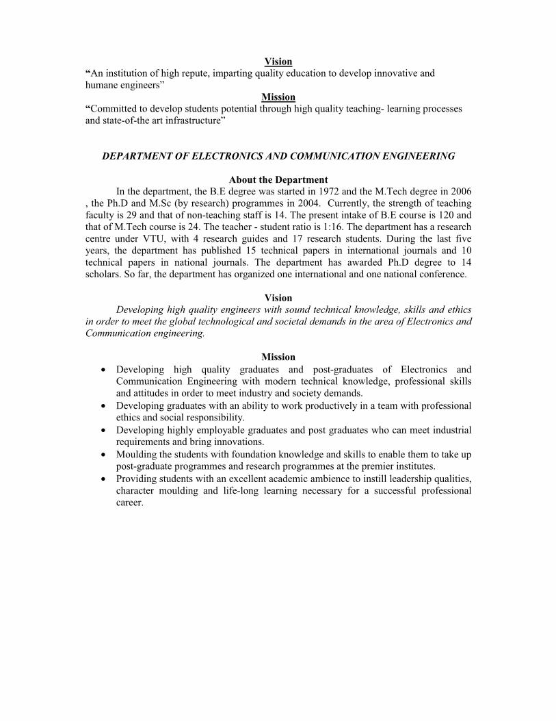
Vision“An institution of high repute, imparting quality education to develop innovative and humane engineers”
Mission“Committed to develop students potential through high quality teaching- learning processes and state-of-the art infrastructure”
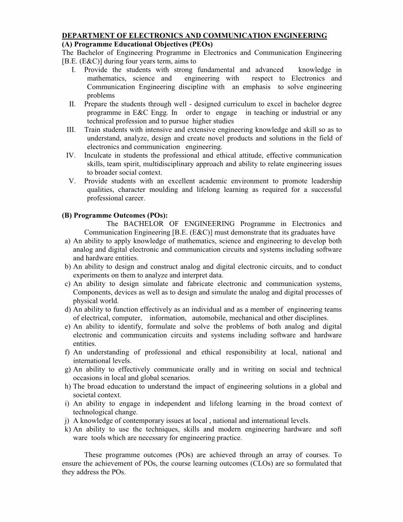
DEPARTMENT OF ELECTRONICS AND COMMUNICATION ENGINEERING
About the DepartmentIn the department, the B.E degree was started in 1972 and the M.Tech degree in 2006
, the Ph.D and M.Sc (by research) programmes in 2004. Currently, the strength of teaching faculty is 29 and that of non-teaching staff is 14. The present intake of B.E course is 120 and that of M.Tech course is 24. The teacher - student ratio is 1:16. The department has a research centre under VTU, with 4 research guides and 17 research students. During the last five years, the department has published 15 technical papers in international journals and 10 technical papers in national journals. The department has awarded Ph.D degree to 14 scholars. So far, the department has organized one international and one national conference.
VisionDeveloping high quality engineers with sound technical knowledge, skills and ethics
in order to meet the global technological and societal demands in the area of Electronics and Communication engineering.
Mission• Developing high quality graduates and post-graduates of Electronics and
Communication Engineering with modern technical knowledge, professional skills and attitudes in order to meet industry and society demands.
• Developing graduates with an ability to work productively in a team with professional ethics and social responsibility.
• Developing highly employable graduates and post graduates who can meet industrial requirements and bring innovations.
• Moulding the students with foundation knowledge and skills to enable them to take up post-graduate programmes and research programmes at the premier institutes.
• Providing students with an excellent academic ambience to instill leadership qualities, character moulding and life-long learning necessary for a successful professional career.
DEPARTMENT OF ELECTRONICS AND COMMUNICATION ENGINEERING(A) Programme Educational Objectives (PEOs) The Bachelor of Engineering Programme in Electronics and Communication Engineering [B.E. (E&C)] during four years term, aims to
I. Provide the students with strong fundamental and advanced knowledge in mathematics, science and engineering with respect to Electronics and Communication Engineering discipline with an emphasis to solve engineering problems
II. Prepare the students through well - designed curriculum to excel in bachelor degree programme in E&C Engg. In order to engage in teaching or industrial or any technical profession and to pursue higher studies
III. Train students with intensive and extensive engineering knowledge and skill so as to understand, analyze, design and create novel products and solutions in the field of electronics and communication engineering.
IV. Inculcate in students the professional and ethical attitude, effective communication skills, team spirit, multidisciplinary approach and ability to relate engineering issues to broader social context.
V. Provide students with an excellent academic environment to promote leadership qualities, character moulding and lifelong learning as required for a successful professional career.
(B) Programme Outcomes (POs): The BACHELOR OF ENGINEERING Programme in Electronics and
Communication Engineering [B.E. (E&C)] must demonstrate that its graduates have a) An ability to apply knowledge of mathematics, science and engineering to develop both
analog and digital electronic and communication circuits and systems including software and hardware entities.
b) An ability to design and construct analog and digital electronic circuits, and to conduct experiments on them to analyze and interpret data.
c) An ability to design simulate and fabricate electronic and communication systems, Components, devices as well as to design and simulate the analog and digital processes of physical world.
d) An ability to function effectively as an individual and as a member of engineering teams of electrical, computer, information, automobile, mechanical and other disciplines.
e) An ability to identify, formulate and solve the problems of both analog and digital electronic and communication circuits and systems including software and hardware entities.
f) An understanding of professional and ethical responsibility at local, national and international levels.
g) An ability to effectively communicate orally and in writing on social and technical occasions in local and global scenarios.
h) The broad education to understand the impact of engineering solutions in a global and societal context.
i) An ability to engage in independent and lifelong learning in the broad context of technological change.
j) A knowledge of contemporary issues at local , national and international levels. k) An ability to use the techniques, skills and modern engineering hardware and soft
ware tools which are necessary for engineering practice.
These programme outcomes (POs) are achieved through an array of courses. To ensure the achievement of POs, the course learning outcomes (CLOs) are so formulated that they address the POs.
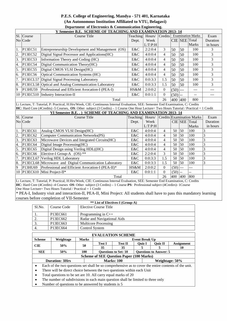
P.E.S. College of Engineering, Mandya - 571 401, Karnataka (An Autonomous Institution Affiliated to VTU, Belagavi)
Department of Electronics & Communication Engineering. V Semester B.E. SCHEME OF TEACHING AND EXAMINATION 2013- 14
Sl. No
Course Code
Course Title Teaching Dept.
Hours/ Week
L:T:P:H
Credits Examination Marks Exam Duration in hours
CIE SEE Total Marks
1. P13EC51 Entrepreneurship Development and Management (OS) E&C 2:2:0:4 3 50 50 100 3 2. P13EC52 Digital Signal Processor and Applications(HC) E&C 4:0:0:4 4 50 50 100 3 3. P13EC53 Information Theory and Coding (HC) E&C 4:0:0:4 4 50 50 100 3 4. P13EC54 Digital Communication Theory(HC) E&C 4:0:0:4 4 50 50 100 3 5. P13EC55 Digital CMOS VLSI Design(HC) E&C 4:0:0:4 4 50 50 100 3 6. P13EC56 Optical Communication Systems (HC) E&C 4:0:0:4 4 50 50 100 3 7. P13ECL57 Digital Signal Processing Laboratory E&C 0:0:3:3 1.5 50 50 100 3 8. P13ECL58 Optical and Analog Communication Laboratory E&C 0:0:3:3 1.5 50 50 100 3 9 P13HU59 Professional and Efficient Avocation-I (PEA-I) HS&M 2:0:0:2 0 (50) --- --- --- 10 P13EC510 Industry Interaction-II E&C 0:0:1:1 0 (50) -- -- ---
Total 26 400 400 800 L: Lecture, T: Tutorial, P: Practical, H:Hrs/Week, CIE: Continuous Internal Evaluation, SEE: Semester End Examination, C: Credits HC: Hard Core (4Credits) -5 Courses, OS: Other subject (3 Credits) – 1 Course One Hour Lecture= Two Hours Tutorial / Practical = 1 Credit
VI Semester B.E. . ) SCHEME OF TEACHING AND EXAMINATION 2013- 14 Sl. No
Course Code
Course Title Teaching Dept.
Hours/ Week
L:T:P:H
Credits Examination Marks Exam Duration in hours
CIE SEE Total Marks
1. P13EC61 Analog CMOS VLSI Design(HC) E&C 4:0:0:4 4 50 50 100 3 2. P13EC62 Computer Communication Networks(PS) E&C 4:0:0:4 4 50 50 100 3 3. P13EC63 Microwave Devices and Integrated Circuits(HC) E&C 4:0:0:4 4 50 50 100 3 4. P13EC64 Digital Image Processing(HC) E&C 4:0:0:4 4 50 50 100 3 5. P13EC65 Digital Design using Verilog HDL((HC) E&C 4:0:0:4 4 50 50 100 3 6. P13EC66 Elective-I Group-A (OS) ** E&C 2:2:0:4 3 50 50 100 3 7. P13ECL67 Verilog HDL Laboratory E&C 0:0:3:3 1.5 50 50 100 3 8. P13ECL68 Microwave and Digital Communication Laboratory E&C 0:0:3:3 1.5 50 50 100 3 9 P13HU69 Professional and Efficient Avocation-I (PEA-II)* HS&M 2:0:0:2 0 (50) --- --- 10 P13EC610 Mini Project-II* E&C 0:0:1:1 0 (50) -- --
Total 26 400 400 800 L: Lecture, T: Tutorial, P: Practical, H:Hrs/Week, CIE: Continuous Internal Evaluation, SEE: Semester End Examination, C: Credits HC: Hard Core (4Credits) -4 Courses OS: Other subject (3 Credits) – 1 Course PS: Professional subject (4Credirs)- 1Course One Hour Lecture= Two Hours Tutorial / Practical = 1 Credit * PEA-I, Industry visit and interaction-II, PEA-II, Mini Project: All students shall have to pass this mandatory learning courses before completion of VII-Semester
** List of Electives-I (Group-A) Sl.No. Course Code Elective Course Title
1. P13EC661 Programming in C++ 2. P13EC662 Radar and Navigational Aids 3. P13EC663 Multicore Processing 4. P13EC664 Control System
EVALUATION SCHEMEScheme Weightage Marks Event Break Up
CIE 50% 50 Test I Test II Quiz I Quiz II Assignment 35 35 5 5 10
SEE 50% 100 Questions to Set: 10 Questions to Answer: 5 Scheme of SEE Question Paper (100 Marks)
Duration: 3Hrs Marks: 100 Weightage: 50% • Each of the two questions set shall be so comprehensive as to cover the entire contents of the unit. • There will be direct choice between the two questions within each Unit • Total questions to be set are 10. All carry equal marks of 20 • The number of subdivisions in each main question shall be limited to three only • Number of questions to be answered by students is 5

Department Of Electronics And Communication Engineering
V & VI Semester Syllabus 2013-2014 ����������������������������������������������������������������
��
Course Learning Objectives (CLOs)This course aims to 1. Provide the basic knowledge of Entrepreneurship and Management. 2. Explain the managerial responsibilities in a typical Engineering career. 3. Provide the understanding of the various functions of technology management. 4. Highlight the nature of technical professionals and the factors for effective motivation. 5. Outline the concepts of entrepreneurship 6. Provide the knowledge of central and state level institutions / agencies supporting small–
business enterprises. 7. Illustrate the procedure for setting up of a small scale industrial unit.
Course ContentUNIT – I
Entrepreneurship: Evolution and concept of entrepreneurship, Entrepreneurship today, Types of entrepreneurship, Intrapreneurship, Entrepreneurial competencies, Capacity building for entrepreneurs Entrepreneurial Development and Training: Entrepreneurial environment, Models of entrepreneurial development, Entrepreneurial motivation, Entrepreneurship training methods, the process of entrepreneurial development Women Entrepreneurs: Women’s entrepreneurship in Asia, Women’s entrepreneurship in India, Challenges faced by women entrepreneurs, Strategies for the development of women entrepreneurs, Institutions supporting women entrepreneurs in India, Special bank schemes promoting women’s entrepreneurship, Women entrepreneur from around the world, Women entrepreneurs in India, Women’s empowerment through entrepreneurship Text 1: Chapters 1, 2 and 3. Pages 2– 18, 21– 40, 43– 67. 11 Hrs
UNIT – II Identification of Business Opportunities: Introduction, Mobility of entrepreneurship, Business opportunities in India, Models for opportunity evaluation Project Management and Financing: Project manager, Project life cycle, Project scheduling, Project management software, Capital budgeting, Generating an investment project proposal, Project analysis, Market analysis, Technical analysis, Financial analysis, Economic analysis, Ecological analysis, Project evaluation and selection, Project financing, Project implementation phase, Capital structure and cost of capital, Detailed project report Institutions Supporting Business Enterprises: Central level institutions, State level institutions, other institutions Text 1: Chapters 6, 7 and 9. Pages 110– 127, 131– 155, 204– 228 11 Hrs
Course Title : ENTREPRENEURSHIP DEVELOPMENT AND MANAGEMENT Course Code: P13EC51 Semester : V L-T-P-H: 2 – 2 – 0-4 Credits:3
Contact Period : Lecture :52 Hrs., Exam: 3Hrs Weightage :CIE:50% SEE:50%
Department Of Electronics And Communication Engineering
V & VI Semester Syllabus 2013-2014 ����������������������������������������������������������������
��
UNIT – III Introduction to Engineering Management: Engineering and Management: Preview, Engineering, Management, Engineering Management: A Synthesis.Historical Development of Engineering Management: Preview, Origins, The Industrial Revolution, Management Philosophies, Scientific Management, Administrative Management, Behavioral Management, Other Contributions.Functions of Technology Management: Planning and Forecasting: Preview, Nature of Planning, The Foundation for Planning, Some Planning Concepts, Forecasting, Stratergies for Managing Technology. Decision Making: Preview, Nature of Decision Making, Management Science, Tools for Decision Making, Computer–Based Information Systems, Implementation. Text 2: Chapters 1, 2, 3 and 4. Pages 1 to 106. 10 Hrs
UNIT – IV Functions of Technology Management (Continued): Organizing: Preview, Nature of organizing, Traditional Organization Theory, Technology and Modern Organization Structures, Teams. Some Human Aspects of Organizing: Preview, Staffing Technical Organizations, Authority and Power, Delegation, Committees and meetings. Motivating and Leading Technical People: Preview, Motivation, Leadership, Motivating and Leading Technical Professionals.Controlling: Preview, The Process of Control, Financial Controls, Nonfinancial Controls.Text 2: Chapters 5, 6, 7 and 8. Pages 107 to 196. 10 Hrs
UNIT – V Managing Your Engineering Career: Achieving Effectiveness as an Engineer: Preview, Getting Off to the Right Start, Charting Your Career, Communicating Your Ideas, Staying Technically Competent, Professional Activity Managerial and International Opportunities for Engineers: Preview, Management and the Engineer, International management. Special Topics in Engineering Management: Preview, Women and Minorities in Engineering and Management, Managing Your Time, Professional Ethics and Conduct, Future Considerations in Engineering and Management.Text 2: Chapters 16, 17 and 18. Pages 391 to 486. 10 Hrs
TEXT BOOKS: 1. “Entrepreneurship Development and Small Business Enterprises”, Poornima M.
Charantimath, 2nd Edition, Pearson Education 2. “Managing Engineering and Technology”, Lucy C. Morse and Daniel L. Babcock, 3rd
Edition, PHI REFERENCE BOOKS:
1. “Essentials of management”, Koontz, Weirich, 9th Edition, Tata McGraw Hill, Publication year 2012
2. “Entrepreneurship”, Arya Kumar, Dorling Kindersley (India) Pvt., Publication year 2012
3. “Entrepreneurship”, Rajeev Roy, 2nd Edition, Oxford University Press
Department Of Electronics And Communication Engineering
V & VI Semester Syllabus 2013-2014 ���������������������������������������������������������������
��
Course Outcome (CO)After learning all the units of the course, the student is able to 01 Outline the evolution and concepts of entrepreneurship. – L1 (Unit – I) 02 Explain the concept of project management. – L2 (Unit – II) 03 Describe the origins of engineering management. – L1 (Unit – III) 04 Explain the balance sheets, income statements and ratios. – L2 (Unit – IV) 05 Explain the importance of ethics in engineering. – L2 (Unit – V) 06 Describe the situations where conflict of interest may arise. – L1 (Unit – V)
Topic Learning OutcomesAfter learning all the topics of UNIT– I, the student is able to
01 Explain the concept of entrepreneur. – L2 02 Discuss the evolution of the concept of entrepreneurship. – L2 03 Illustrate the various sources of innovation, with examples. – L3 04 Examine the factors that motivate people to go into business. – L4 05 Discuss the necessity of entrepreneurial motivation for a successful entrepreneurial
career. – L2 06 Explain the factors that motivate people to become entrepreneurs. – L2 07 Discuss the concept, objectives and stages of entrepreneurship development programmes
(EDPs). – L2 08 Discuss the importance of women entrepreneurs. – L209 Explain the factors and strategies needed for the development of women entrepreneurs in
India. – L2 10 Outline the growth of women entrepreneurs in India. – L1
After learning all the topics of UNIT– II, the student is able to 01 Analyze the difference between an idea and an entrepreneurial opportunity. – L4 02 Explain the factors to be considered for generating business ideas. – L5 03 Identify the major changes that create opportunities for entrepreneurs. – L2 04 Explain the John Mullin’s seven– domain framework. – L2 05 Discuss the six broad phases of capital budgeting. – L2 06 Illustrate the schematic diagram of the project feasibility study. – L4 07 Sketch the schematic diagram depicting the formalities for setting up a business
enterprise. – L3 08 Solve the numerical problems on project management and financing. – L3 09 Describe the institutional set up for entrepreneurial development of India. – L2 10 Explain the role of national– level training institutes in conducting EDPs. – L2
After learning all the topics of UNIT– III, the student is able to 01 Define the management, engineering and engineering management. – L1 02 Explain the need for engineers in management. – L2 03 Describe the various roles of a manager according to Henry Mintzberg. – L2 04 Explain the five functions of managers according to Henry Fayol. – L2 05 Interpret the F. W. Taylor’s contribution to management. – L3 06 Recognize the contribution of Gilberth’s to management. – L1 07 Illustrate the planning/decision making process. – L3 08 Interpret the Peter Drucker’s concept of management by objectives. – L3 09 Summarize the strategies for managing technology. – L2 10 Explain the technological forecasting. – L2

Department Of Electronics And Communication Engineering
V & VI Semester Syllabus 2013-2014 ���������������������������������������������������������������
��
After learning all the topics of UNIT– IV, the student is able to 01 List the legal forms of organization and explain them. – L1 02 Describe the factors determining effective span of control. – L2 03 Analyze the Woodward and Aston studies related to standardized organizational
environment. – L4 04 Discuss the strategy you propose to use in your personal career to assure you will remain
in demand in a changing, competitive world. – L2 05 Discuss the impact of information revolution on organizations. – L2 06 Describe the assignment, delegation and accountability. – L2 07 List the barriers to delegation for engineers. – L108 Explain the leadership styles as proposed by Tannenbaum and Schmidt. – L2 09 Explain the Douglas McGregor’s Theory X and Theory Y postulates with respect to
motivation. – L2 10 Differentiate between the scientists and the engineers. – L4
After learning all the topics of UNIT– V, the student is able to 01 Discuss the core concepts in engineering ethics. – L2 02 Summarize the ethical problems in industrial practice. – L2 03 Analyze the “career stages” of Super and /or those of Dalton and Thomspson. – L4 04 Define the Communication and explain the importance of communication. – L1 05 List the career problems of the woman engineer? – L1 06 List the six stages of multi– nationalization according to Jacoby. – L1 07 Explain the Japanese management styles. – L2 08 Discuss the various International trade agreements. – L2 09 Discuss the management in developing countries. – L2 10 Explain the need for engineers in top management. – L2
Review Questions1. Explain how an entrepreneur differs from a manager.2. Explain the characteristics of a successful entrepreneur. 3. Discuss the development methods of achievement motivation. 4. Discuss the challenges in the path of women’s entrepreneurship. 5. List the institutions supporting women’s entrepreneurship in India. 6. Describe the various types of entrepreneurial development programmes available in India. 7. Classify the business opportunities based on origin, application, user or source and
external sources of change. 8. Explain how “solving a problem” can create a business opportunity. 9. Describe the institutional set up for entrepreneurial development of India. 10. Discuss the need for institutional support for MSME. 11. Discuss the need for institutional support for MSME. 12. Explain the functions of District Industries Centers. 13. Identify the three types of skills needed by an effective manager as conceived by Robert
L.Katz 14. Describe how the relative need of the three types of skills vary with the level of
management. 15. Discuss the function of managers at various management levels. 16. Defend the Max Weber’s model of bureaucracy. 17. Summarize the Hawthorne studies. 18. Discuss the Henri Fayol’s advice to the future engineers. 19. Solve the numerical problems on planning and forecasting.

Department Of Electronics And Communication Engineering
V & VI Semester Syllabus 2013-2014 ����������������������������������������������������������������
��
20. List the three occasions for decision as cited by Chester Barnard. 21. Explain why the Barnard thought that the third category is most important. 22. Explain the difference between “optimizing” and “sufficing” in making decisions. 23. Distinguish between the routine and non–routine decisions. 24. Solve the numerical problems on decision making. 25. Discuss the three questions posed by Peter Drucker to help identify the key activities. 26. Explain the decision analysis and relation analysis according to Peter Drucker. 27. Discuss the various patterns of departmentation? 28. Explain the process of hiring technical professionals. 29. Interpret the job requisition/description. Illustrate a typical job requisition. 30. Interpret the orientation, training and appraising performance. 31. Explain the acceptance theory of authority. 32. List the sources of power and explain them. 33. Describe the committees and meetings. 34. 34.Illustrate the Blake and Mouton’s Leadership grid. 35. Summarize the Frederick Herzberg’s two factor theory. 36. List the David McClelland’s trio of needs and explain them. 37. Sketch the Victor Vroom’s Expectancy theory. 38. Illustrate the steps involved in the control process 39. List the characteristics of effective control systems. 40. Describe the budgeting process. 41. Solve the numerical problems on financial control. 42. Explain the three types of forces that a manager should consider as proposed by
Tannenbaum and Schmidt. 43. Outline the various motivation theories 44. Label the Abraham Maslow’s hierarchy of needs. 45. Summarize the B.F.Skinner’s behaviour modification theory. 46. Explain the Rosenbaum’s five strategic dimensions of technical leadership. 47. Illustrate the communications process model. 48. List the various communication tools of special importance to the engineer. 49. Identify the threats to staying technically competent. 50. List the difference between engineers and engineer managers.
Lesson PlanUNIT – I
Period No. Topics
1. Entrepreneurship: Evolution and concept of entrepreneurship, 2. Entrepreneurship today, Types of entrepreneurship, Intrapreneurship, 3. Entrepreneurial competencies, Capacity building for entrepreneurs 4. Entrepreneurial environment, Models of entrepreneurial development, 5. Entrepreneurial motivation, Entrepreneurship training methods, 6. the process of entrepreneurial development 7. Women’s entrepreneurship in Asia, Women’s entrepreneurship in India, Challenges faced
by women entrepreneurs, 8. Strategies for the development of women entrepreneurs, Institutions supporting women entrepreneurs in India
8. Special bank schemes promoting women’s entrepreneurship, Women entrepreneur from around the world,
9. Women entrepreneurs in India, Women’s empowerment through entrepreneurship
Department Of Electronics And Communication Engineering
V & VI Semester Syllabus 2013-2014 ����������������������������������������������������������������
��
UNIT – II Period No. Topics 1. Identification of Business Opportunities: Introduction, Mobility of entrepreneurship, 2. Business opportunities in India, Models for opportunity evaluation 3. Project Management and Financing: Project manager, 4. Project life cycle, Project scheduling, Project management software, 5. Capital budgeting, Generating an investment project proposal, 6. Project analysis, Market analysis, Technical analysis, Financial analysis, 7. Economic analysis, Ecological analysis, Project evaluation and selection, 8. Capital structure and cost of capital Detailed project report 9. Project financing, Project implementation phase, 10. Supporting Business Enterprises: Central level institutions, 11. State level institutions 12. Other institutions
UNIT – III Period No. Topics 1. Introduction to Engineering Management: Engineering and Management: Preview,
Engineering, 2. Management, Engineering Management: A Synthesis. 3. Historical Development of Engineering Management: Preview, Origins, The Industrial
Revolution, Management Philosophies, 4. Scientific Management, Administrative Management, Behavioural Management, Other
Contributions. 5. Functions of Technology Management: Planning and Forecasting: Preview, Nature of
Planning, 6. The Foundation for Planning, Some Planning Concepts, Forecasting, 7. Strategies for Managing Technology. Decision Making: Preview, Nature of Decision
Making, 8. Management Science, Tools for Decision Making, 9. Computer–Based Information Systems, 10. Implementation.
UNIT – IV Period No. Topics 1. Functions of Technology Management (Continued): Organizing: Preview, Nature of
organizing, 2. Traditional Organization Theory, Technology and Modern Organization Structures,
Teams. 3. Some Human Aspects of Organizing: Preview, Staffing Technical Organizations, 4. Authority and Power, Delegation, Committees and meetings. 5. Motivating and Leading Technical People: Preview, Motivation, 6. Leadership, Motivating and Leading Technical Professionals. 7. Controlling: Preview, The Process of Control, 8. Financial Controls, 9. Nonfinancial Controls.

Department Of Electronics And Communication Engineering
V & VI Semester Syllabus 2013-2014 �������������������������������������������������������������� �
��
UNIT – V Period No. Topics 1. Managing Your Engineering Career: Achieving Effectiveness as an Engineer: Preview, 2. Getting Off to the Right Start, Charting Your Career, 3. Communicating Your Ideas, Staying Technically Competent, 4. Professional Activity 5. Managerial and International Opportunities for Engineers: Preview, Management and the
Engineer, 6. International management. 7. Special Topics in Engineering Management: Preview, 8. Women and Minorities in Engineering and Management, 9. Managing Your Time, 10. Professional Ethics and Conduct, 11. Future Considerations in Engineering and Management.
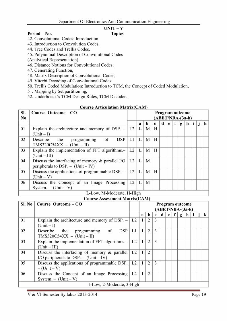
Course Articulation Matrix (CAM)Sl. No
Course Outcome – (CO) Program outcome (ABET/NBA-(3a-k)
a b c d e f g h i j k01 Outline the evolution and concepts of
entrepreneurship. – (Unit – I) L1 M M L
02 Explain the concept of project management. –(Unit – II)
L2 M H
03 Describe the origins of engineering management. –(Unit – III)
L1 M M L
04 Explain the balance sheets, income statements and ratios. – (Unit – IV)
L2 M H
05 Explain the importance of ethics in engineering. –(Unit – V)
L2 M M L
06 Describe the situations where conflict of interest may arise. –(Unit – V)
L1 M L
L-Low, M-Moderate, H-HighCourse Assessment Matrix (CAM)
Sl. No
Course Outcome – CO Program outcome (ABET/NBA-(3a-k)
a b c d e f g h i j k01 Outline the evolution and concepts of
entrepreneurship. – (Unit – I) L1 1 2 1
02 Explain the concept of project management. –(Unit – II)
L2 2 3
03 Describe the origins of engineering management. –(Unit – III)
L1 2 2 1
Explain the balance sheets, income statements and ratios. – (Unit – IV)
L2 2 1
05 Explain the importance of ethics in engineering. –(Unit – V)
L2 2 2 3
06 Describe the situations where conflict of interest may arise. –(Unit – V)
L1 2 3
1-Low, 2-Moderate, 3-High
Department Of Electronics And Communication Engineering
V & VI Semester Syllabus 2013-2014 ����������������������������������������������������������������
��
�
Course Title : DIGITAL SIGNAL PROCESSOR AND APPLICATIONS Course Code: P13EC52 Semester : V L-T-P-H: 4 – 0 – 0-4 Credits:4
Contact Period : Lecture :52 Hrs., Exam: 3Hrs. Weightage :CIE:50% SEE:50%
Prerequisite course for: 1. Embedded and Real Time Systems – P13EC73
Course Learning Objectives (CLOs)This course aims to 1. Provide the understanding of architecture, programming and interfacing of commercially
available Digital Signal Processor. 2. Explain the effective use of Digital Signal Processor in system implementation. 3. Adopt the MATLAB tools in DSP applications. 4. Provide the understanding of architecture features of TMS320C54XX. 5. Describe the programming of TMS320C54XX for several basic DSP algorithms. 6. Explain the interfacing procedure to use programmable Digital Signal Processor. 7. Discuss the applications of programmable DSP devices.
Course ContentUNIT – I
Architectures for Programmable DSP Devices: Introduction, Basic Architectural Features, DSP Computational Building Blocks, Bus Architecture and Memory, Data Addressing Capabilities, Address Generation Unit, Programmability and Program Execution, Speed Issues, Features for External Interfacing. Text: 4.1 to 4.10 10 Hrs
UNIT – II Programmable Digital Signal Processors: Introduction, Commercial Digital Signal– processing Devices, Data Addressing Modes of TMS32OC54xx DSPs, Data Addressing Modes of TMS32OC54xx Processors, Memory Space of TMS32OC54xx Processors, Program Control, TMS32OC54xx Instructions and programming, On–chip Peripherals, Interrupts of TMS32OC54xx Processors, Pipeline Operation of TMS32OC54xx Processors. Text: 5.1 to 5.10 10 Hrs
UNIT – III Implementation of Basic DSP Algorithms: Introduction, the Q– notation, FIR Filters, IIR Filters, Interpolation Filters, Decimation Filters, PID controller, Adaptive Filters, 2–D Signal Processing. Implementation of FFT Algorithms: Introduction, an FFT Algorithm for DFT Computation, Overflow and Scaling, Bit–Reversed Index Generation, an 8 Point FFT Implementation on the TMS32OC54xx, Computation of Signal Spectrum. Text: 7.1 to 7.10 and 8.1 to 8.7 11 Hrs
UNIT – IV Interfacing Memory and Parallel I/O Peripherals to Programmable DSP Devices: Introduction, Memory Space Organization, External Bus Interfacing Signals, Memory Interface, Parallel I/O Interface, Programmed I/O, Interrupts and I/O, Direct Memory Access (DMA).

Department Of Electronics And Communication Engineering
V & VI Semester Syllabus 2013-2014 ����������������������������������������������������������������
��
Interfacing and Applications of DSP Processor: Introduction, Synchronous Serial Interface, A Multichannel Buffered Serial Port (McBSP), McBSP Programming, A CODEC Interface Circuit, CODEC Programming, A CODEC–DSP Interface example. Text: 9.1 to 9.8 and 10.1 to10.7 11 Hrs
UNIT – V
Applications of Programmable DSP Devices: Introduction, A DSP system, DSP Based Bio– telemetry Receiver, A Speech Processing System, An Image Processing System, A Position control system for a hard disk drive, DSP based Power meter. Text: 11.1 to 11.7 10 Hrs
TEXT BOOK: ”Digital Signal Processing”, Avatar Singh and S. Srinivasan, Thomson Learning, 2004.
REFERENCE BOOKS: 1. “Digital Signal Processing”, A practical approach, Ifeachor E. C.,Jervis B. W Pearson–
Education, PHI/ 2002 2. “Digital Signal Processors”, B Venkataramani and M Bhaskar TMH, 2002 3. “Architectures for Digital Signal Processing”, Peter Pirsch John Weily, 2007
Course Outcomes After learning all the units of the course, the student is able to
01 Explain the architecture and memory of DSP. – L2 (Unit – I) 02 Describe the programming of DSP TMS320C54XX. – L1 (Unit – II) 03 Explain the implementation of FFT algorithms. – L2 (Unit – III) 04 Discuss the interfacing of memory & parallel I/O peripherals to DSP. – L2 (Unit – IV) 05 Discuss the applications of programmable DSP. – L2 (Unit – V) 06 Discuss the Concept of an Image Processing System. – L2 (Unit – V)
Topic Learning OutcomesAfter learning all the topics of UNIT– I, the student is able to
01 Explain the basic architectural Features of DSP. – L2 02 Describe the DSP computational building blocks –L1 03 Explain the bus structures and memory of DSP. – L2 04 Discuss the different addressing modes used in DSP. – L2 05 Explain the operation of address generation unit. – L2 06 Explain the execution of programs in DSP. – L2 07 Explain the Speed Issues related to the DSP Architecture. – L2
After learning all the topics of UNIT– II, the student is able to 01 Discuss the various commercially available DSP devices. – L2 02 Explain the memory organization of TMS320C54XX. – L2 03 Describe the different addressing mode of TMS320C54XX. – L1 04 Describe the Memory Space of TMS320C54XX Processors. – L1 05 Describe the program control in DSP. – L1 06 Discuss the instruction set of TMS320C54XX. – L2 07 Explain the programming of TMS320C54XX. – L2 08 Explain the on– chip peripherals of TMS320C54XX. – L209 Explain the Pipeline operation of TMS320C54XX. – L2
Department Of Electronics And Communication Engineering
V & VI Semester Syllabus 2013-2014 �����������������������������������������������������������������
��
After learning all the topics of UNIT– III, the student is able to 01 Describe the Q– notation used in MATLAB. – L1 02 Write the program of IIR filters using MATLAB tool. – L3 03 Explain the concept of interpolation and decimation in filters. – L2 04 Explain the concept of PID Controller, Adaptive Filters, 2–D Signal Processing. – L2 05 Explain the FFT algorithm used for DFT computation. – L2 06 Describe the butterfly computation structure. – L1 07 Explain the overflow and scaling problem. – L2 08 Explain the bit reversed index generation in DFT Computation. – L2 09 Explain the 8– point FFT implementation on TMS320C54XX. – L2
After learning all the topics of UNIT– IV, the student is able to 01 Explain the memory space organization in TMS320C54XX. – L2 02 Discuss the different external bus interfacing signals. – L2 03 Explain the interfacing of memory to TMS320C54XX. – L2 04 Explain the interfacing of parallel and programmed I/O to TMS320C54XX. – L2 05 Explain the interfacing of interrupts and I/O to TMS320C54XX. – L2 06 Explain the operation of DMA in TMS320C54XX. – L2 07 Discuss the synchronous serial interface to TMS320C54XX. – L2 08 Explain the Multichannel Buffered Serial Port (McBSP) and Programming. – L2 09 Explain the CODEC–DSP interface Example. – L2
After learning all the topics of UNIT– V, the student is able to 01 Explain the concept of DSP system. – L2 02 Explain the application of DSP in biotelemetry receiver. – L2 03 Explain the application of DSP in speech processing system. – L2 04 Explain the application of DSP in image processing system. – L2 05 Discuss the Image processing System. – L2 06 Explain the concept of Position Control System for a Hard Disk Drive. – L2 07 Explain the application of DSP–Based Power Meter. – L2
Review Questions
1. Explain the detail study of TMS320C54XX. – L2 (Unit – II) 2. Discuss the implementation of basic DSP algorithms. – L2 (Unit – III) 3. Explain the synchronous serial interface to DSP. – L2 (Unit – IV) 4. Discuss the different interrupts used in TMS320C54XX. – L2 5. Discuss the different addressing modes of TMS320C54XX. – L2 6. Write the program of FIR filters using MATLAB tool. – L3 7. Explain the CODEC interface circuit and CODEC Programming. – L2 8. Explain the basic architectural Features of DSP. – L2 9. Describe the DSP computational building blocks –L1 10. Explain the bus structures and memory of DSP. – L2 11. Discuss the different addressing modes used in DSP. – L2 12. Explain the operation of address generation unit. – L2 13. Explain the execution of programs in DSP. – L2 14. Explain the Speed Issues related to the DSP Architecture. – L2 15. Discuss the various commercially available DSP devices. – L2 16. Explain the memory organization of TMS320C54XX. – L2
Department Of Electronics And Communication Engineering
V & VI Semester Syllabus 2013-2014 �����������������������������������������������������������������
��
17. Describe the different addressing mode of TMS320C54XX. – L1 18. Describe the Memory Space of TMS320C54XX Processors. – L1 19. Describe the program control in DSP. – L1 20. Discuss the instruction set of TMS320C54XX. – L2 21. Explain the programming of TMS320C54XX. – L2 22. Explain the on– chip peripherals of TMS320C54XX. – L223. Explain the Pipeline operation of TMS320C54XX. – L224. Describe the Q– notation used in MATLAB. – L1 25. Write the program of IIR filters using MATLAB tool. – L3 26. Explain the concept of interpolation and decimation in filters. – L2 27. Explain the concept of PID Controller, Adaptive Filters, 2–D Signal Processing. – L2 28. Explain the FFT algorithm used for DFT computation. – L2 29. Describe the butterfly computation structure. – L1 30. Explain the overflow and scaling problem. – L2 31. Explain the bit reversed index generation in DFT Computation. – L2 32. Explain the 8– point FFT implementation on TMS320C54XX. – L2 33. Explain the memory space organization in TMS320C54XX. – L2 34. Discuss the different external bus interfacing signals. – L2 35. Explain the interfacing of memory to TMS320C54XX. – L2 36. Explain the interfacing of parallel and programmed I/O to TMS320C54XX. – L2 37. Explain the interfacing of interrupts and I/O to TMS320C54XX. – L2 38. Explain the operation of DMA in TMS320C54XX. – L2 39. Discuss the synchronous serial interface to TMS320C54XX. – L2 40. Explain the Multichannel Buffered Serial Port (McBSP) and Programming. – L2 41. Explain the CODEC–DSP interface Example. – L2 42. Explain the concept of DSP system. – L2 43. Explain the application of DSP in biotelemetry receiver. – L2 44. Explain the application of DSP in speech processing system. – L2 45. Explain the application of DSP in image processing system. – L2 46. Discuss the Image processing System. – L2 47. Explain the concept of Position Control System for a Hard Disk Drive. – L2 48. Explain the application of DSP–Based Power Meter. – L249. Describe the Programmability, Program Execution and Speed Issues of DSP
architecture. – L1 50. Describe clipping autocorrelation pitch detector with a neat block diagram – L1
Lesson PlanUNIT – I
Period No. Topics 1. Architectures for Programmable DSP Devices: Introduction 2. Basic Architectural Features 3. DSP Computational Building Blocks 4. Bus Architecture and Memory 5. Data Addressing Capabilities 6. Address Generation Unit 7. Programmability and Program Execution 8. Programmability and Program Execution 9. Speed Issues, 10. Features for External Interfacing
Department Of Electronics And Communication Engineering
V & VI Semester Syllabus 2013-2014 �����������������������������������������������������������������
��
UNIT – II Period No. Topics 11. Programmable Digital Signal Processors: Introduction 12. Commercial Digital Signal– processing Devices 13. Data Addressing Modes of TMS32OC54xx DSPs 14. Data Addressing Modes of TMS32OC54xx Processors 15. Memory Space of TMS32OC54xx Processors 16. Program Control 17. TMS32OC54xx Instructions and programming 18. On–chip Peripherals 19. Interrupts of TMS32OC54xx Processors 20. Pipeline Operation of TMS32OC54xx Processors
UNIT – III Period No. Topics 21. Implementation of Basic DSP Algorithms: Introduction 22. The Q– notation, FIR Filters 23. IIR Filters, Interpolation Filters 24. Decimation Filters, PID controller 25. Adaptive Filters, 2–D Signal Processing 26. Implementation of FFT Algorithms: Introduction 27. An FFT Algorithm for DFT Computation 28. Overflow and Scaling 29. Bit–Reversed Index Generation 30. An 8 Point FFT Implementation on the TMS32OC54xx 31. Computation of Signal Spectrum
UNIT – IV Period No. Topics
32. Interfacing Memory and Parallel I/O Peripherals to Programmable DSP Devices: Introduction
33. Memory Space Organization 34. External Bus Interfacing Signals 35. Memory Interface 36. Parallel I/O Interface, Programmed I/O 37. Interrupts and I/O, Direct Memory Access (DMA) 38. Interfacing and Applications of DSP Processor: Introduction 39. Synchronous Serial Interface 40. A Multichannel Buffered Serial Port (McBSP), McBSP Programming 41. A CODEC Interface Circuit 42. CODEC Programming, A CODEC–DSP Interface example.
Department Of Electronics And Communication Engineering
V & VI Semester Syllabus 2013-2014 ����������������������������������������������������������������
��
UNIT – V Period No. Topics 43. Applications of Programmable DSP Devices: Introduction 44. Introduction 45. A DSP system 46. DSP Based Bio– telemetry Receiver 47. DSP Based Bio– telemetry Receiver 48. A Speech Processing System 49. An Image Processing System 50. A Position control system for a hard disk drive 51. A Position control system for a hard disk drive 52. DSP based Power meter.
Course Articulation Matrix(CAM)Sl. No
Course Outcome – CO Program outcome (ABET/NBA-(3a-k)
a b c d e f g h i j k01 Explain the architecture and memory of DSP. –
(Unit – I) L2 L M H
02 Describe the programming of DSP TMS320C54XX. – (Unit – II)
L1 L M H
03 Explain the implementation of FFT algorithms.– (Unit – III)
L2 L M H
04 Discuss the interfacing of memory & parallel I/O peripherals to DSP. – (Unit – IV)
L2 L M
05 Discuss the applications of programmable DSP. – (Unit – V)
L2 L M H
06 Discuss the Concept of an Image Processing System. – (Unit – V)
L2 L M
L-Low, M-Moderate, H-High
Course Assessment Matrix (CAM)Sl. No
Course Outcome – CO Program outcome (ABET/NBA-(3a-k)
a b c d e f g h i j k01 Explain the architecture and memory of DSP. –
(Unit – I) L2 1 2 3
02 Describe the programming of DSP TMS320C54XX. – (Unit – II)
L1 1 2 3
03 Explain the implementation of FFT algorithms.– (Unit – III)
L2 1 2 3
04 Discuss the interfacing of memory & parallel I/O peripherals to DSP. – (Unit – IV)
L2 1 2
05 Discuss the applications of programmable DSP. – (Unit – V)
L2 1 2 3
06 Discuss the Concept of an Image Processing System. – (Unit – V)
L2 1 2
1-Low, 2-Moderate, 3-High

Department Of Electronics And Communication Engineering
V & VI Semester Syllabus 2013-2014 ����������������������������������������������������������������
��
Course Title : INFORMATION THEORY AND CODING Course Code: P13EC53 Semester : V L-T-P-H: 4 – 0 – 0-4 Credits:4 Contact Period : Lecture :52 Hrs., Exam: 3Hrs. Weightage :CIE:50% SEE:50%
This Course forms a prerequisite course for 1. Computer Communication Networks – P13EC62 2. GSM Communication and Networks – P13EC 74 3. Satellite Communication – P13EC81
Course Learning Objectives (CLOs)This course aims to 1. Provide the knowledge of information theory and source coding theorem. 2. Analyze the efficient data compression methods and describe the most efficient
compression method. 3. Develop the channel model and channel capacity theorem. 4. Describe the linear block code and parity check matrix. 5. Explain the probability of error correction, hamming codes and cyclic codes. 6. Explain the matrix description of convolution codes, decoding of convolution codes &
concept of trellis coded modulation.
Course ContentUNIT – I
Source Coding 1: Introduction to Information theory, Uncertainty and Information, Average Mutual Information and Entropy, Information Measures for Continuous Random Variables, Source coding theorem. Source Coding 2: Huffman Coding, Arithmetic Coding, The Lempel– Ziv Algorithm, Run Length Encoding and the PCX format, Introduction to Image Compression, The JPEG standard for Lossless Compression, the JPEG standard for Lossy Compression. Text: 1.1 to 1.5, 1.6, 1.8, 1.9, 1.10, 1.14 to 1.16 11 Hrs
UNIT – II Channel Capacity and coding: Introduction, channel Models, Channel Capacity, Information Capacity Theorem, the Shannon Limit, and Random Selection of Codes.Text: 2.1 to 2.3, 2.5, 2.6, 2.8 10 Hrs
UNIT – III Linear Block Codes for Error Correction 1: Introduction to Error Correcting Codes, Basic Definitions, and Matrix Description of Linear Block codes, Equivalent Codes, Parity Check Matrix, and Decoding of a Linear Block Code. Linear Block Codes for Error Correction 2: Syndrome Decoding, Error Probability after Coding (Probability of Error correction), Perfect Codes, Hamming Codes, Optimal Linear Codes, and Maximum Distance Separable (MDS) Codes. Text: 3.1 to 3.6, 3.7 to 3.10, 3.12, 3.13 10 Hrs
UNIT – IV Cyclic Codes : Introduction to Cyclic Codes, Polynomials, The Division Algorithm for Polynomials, A Method for Generating Cyclic Codes, Matrix Description of Cyclic Codes, Quasi– cyclic Codes and Shortened Cyclic Codes, Burst Error Correction, Fire codes, Golay Codes.

Department Of Electronics And Communication Engineering
V & VI Semester Syllabus 2013-2014 �����������������������������������������������������������������
��
Text: 4.1 to 4.9 10 Hrs UNIT – V
Convolutional Codes: Introduction to Convolution Codes, Tree Codes and Trellis Codes, Polynomial Description of Convolutional Codes (Analytical Representation), Distance Notions for Convolutional Codes, the Generating Function, Matrix Description of Convolutional Codes, Viterbi Decoding of Convolutional Codes. Trellis Coded Modulation: Introduction to TCM, the Concept of Coded Modulation, Mapping by Set partitioning, Underboeck’s TCM Design Rules, TCM Decoder. Text: 6.1 to 6.7, 7.1 to 7.5 11 Hrs
TEXT BOOK: “Information Theory, Coding and Cryptography”, Ranjan Bose, 2rd Edition. Tata McGraw Hill– 2008 REFERENCE BOOKS: 1. “Introduction to communication systems”, K. Sam Shanmugam, John Wiley & Sons. 2. “Communication systems”, Simon Haykin, John Wiley, 4th Ed. 3. “Elements of Information Theory”, Thomas M. Cover, Joy A. Thomas, 2nd edition, John
wiley
Course OutcomeAfter learning all the units of the course, the student is able to 01 Describe the entropy and average mutual information. – L2 (Unit – I) 02 Explain the source coding theorem. – L2 (Unit – I) 03 Describe the JPEG standard for lossy & lossless compression. – L2 (Unit – I) 04 Estimate the capacity of communication channel. – L2 (Unit – II) 05 Explain the linear block codes and its decoding. – L2 (Unit – III) 06 Discuss the cyclic codes, fire codes and golay codes. – L2 (Unit – IV) 07 Compute the convolution codes and trellis code. – L3 (Unit – V) 08 Explain the concept of coded modulation & TCM decoder. – L2 (Unit – V)
Topic Learning Outcome After learning all the topics of UNIT– I, the student is able to 01 Describe the concept of Entropy and Average Mutual Information. – L2 02 Explain the concept of Information theory. – L2 03 Apply the concept of Uncertainty and Information. – L3 04 Develop the expressions for Average Mutual Information and Entropy. – L5 05 Analyze the Information Measures for Continuous Random Variables. – L4 06 Describe the Source coding theorem. – L1 07 Solve the problems on various coding techniques. – L3 08 Describe the Huffman Coding and solve problems on the same. – L2 09 Describe the arithmetic Coding and solve problems on the same. – L1 10 Describe the Lempel– Ziv Algorithm and solve problems on the same. – L1 11 Describe the Run Length Encoding and solve problems on the same. – L1 12 Analyze the JPEG standard for Lossless and lossy Compression. – L4
After learning all the topics of UNIT– II, the student is able to 1. Apply the theorems on channel capacity and Shannon limit. – L3 2. Explain the concept of channel Models. – L2 3. Solve the problems on channel capacity and Shannon limit. – L3 4. Analyze the Random Selection of Codes. – L4

Department Of Electronics And Communication Engineering
V & VI Semester Syllabus 2013-2014 �����������������������������������������������������������������
��
After learning all the topics of UNIT– III, the student is able to 01 Solve the various problems on linear block codes for error correction. – L3 02 Explain the concept of Error Correcting Codes. – L203 Describe the matrix representation of Linear Block codes. – L2 04 Explain the concept of Equivalent Codes and Parity Check Matrix. – L2 05 Analyze the Decoding of a Linear Block Code. – L4 06 Analyze the concept of Syndrome Decoding. – L4 07 Describe the Error Probability after Coding (Probability of Error correction). – L2 08 Illustrate the Perfect Codes. – L4 09 Solve the problems on Hamming Codes. – L3 10 Explain the concept of Optimal Linear Codes and Maximum Distance Separable
(MDS) Codes. – L2
After learning all the topics of UNIT– IV, the student is able to 01 Solve the problems on cyclic codes. – L3 02 Explain the concept of Cyclic Codes. – L2 03 Define the Polynomials. – L1 04 Illustrate the Division Algorithm for Polynomials. – L3 05 Define the Method for Generating Cyclic Codes. – L1 06 Illustrate the Matrix Description of Cyclic Codes. – L3 07 Analyze the concept of Quasi– cyclic Codes and Shortened Cyclic Codes. – L4 08 Explain the concept Burst Error Correction, Fire codes and Golay Codes. – L2
After learning all the topics of UNIT– V, the student is able to 01 Explain the concept of convolutional codes for encoding. – L2 02 Describe the Tree Codes and Trellis Codes. – L2 03 Analyze the Polynomial Description Of Convolutional Codes. – L4 04 Define the Distance Notions for Convolutional Codes. – L1 05 Describe the Matrix representation of Convolutional Codes. – L1 06 Analyze the Viterbi Decoding of Convolutional Codes. – L4 07 Describe the trellis coded modulation techniques. – L2 08 Analyse the Concept of Coded Modulation. – L4 09 Define the Mapping by set partitioning. – L1 10 Illustrate the Underboeck’s TCM Design Rules. – L3 11 Describe the TCM Decoder. – L2
Review Questions01 Apply the concept of Uncertainty and Information. 02 Justify that self information content of a message is a logarithm function of its probability
of emission. 03 Explain the concept of Information theory. 04 Find an expression for average information content of symbols in long independent
sequences. 05 State and prove kraft inequality. 06 Describe the Source coding theorem. 07 Describe the JPEG standard for lossy & lossless compression. 08 Describe the Huffman Coding. 09 Describe the Lempel– Ziv Algorithm. 10 Describe the arithmetic Coding.

Department Of Electronics And Communication Engineering
V & VI Semester Syllabus 2013-2014 ��������������������������������������������������������������� �
��
11 Describe the Run Length Encoding. 12 Apply the theorems on channel capacity and Shannon limit. 13 Explain the concept of channel Models. 14 Analyze the Random Selection of Codes. 15 State and prove Shannon Hartley law. 16 Derive an expression for the upper limit on channel capacity as the band width tents to �. 17 Derive information capacity theorem. 18 Explain channel capacity for MIMO systems. 19 Explain the concept of Error Correcting Codes. 20 Explain the concept of Equivalent Codes and Parity Check Matrix. 21 Analyze the Decoding of a Linear Block Code. 22 Describe the Error Probability after Coding (Probability of Error correction ). 23 Illustrate the Perfect Codes. 24 Explain concept of syndrome decoding. 25 Explain the concept of Optimal Linear Codes and Maximum Distance Separable (MDS)
Codes. 26 Describe perfect code and Hamming code. 27 Define the Polynomials. 28 Analyze the concept of Quasi– cyclic Codes and Shortened Cyclic Codes. 29 Explain the concept Fire codes and Golay Codes. 30 Define the Polynomials. 31 Illustrate the Division Algorithm for Polynomials. 32 Explain the matrix description of convolution code.33 Describe the Tree Codes and Trellis Codes. 34 Illustrate burst error correction . 35 Explain the concept of convolutional codes for encoding. 36 Analyze the Polynomial Description Of Convolutional Codes. 37 Define the Distance Notions for Convolutional Codes. 38 Explain the method for generating cyclic codes. 39 Explain cyclic code & their generation from generating polynomials. 40 Analyse the Concept of Coded Modulation. 41 Describe the Tree Codes and Trellis Codes. 42 Define the Mapping by set partitioning. 43 Illustrate the Underboeck’s TCM Design Rules. 44 Describe the TCM Decoder. 45 Compute the convolution codes and trellis code. 46 Define the Distance Notions for Convolutional Codes. 47 Draw &explain the general structure of TCM encoder that processes m input bits. 48 List advantages & applications of viterbi decoding of convolution codes. 49 Explain the concept of Trellis coded modulation & its demodulation. 50 Define free Euclidean distance and asymptotic coding gain.
Department Of Electronics And Communication Engineering
V & VI Semester Syllabus 2013-2014 �����������������������������������������������������������������
��
Lesson PlanUNIT – I
Period No. Topics 1. Source Coding 1: Introduction to Information theory, 2. Uncertainty and Information, 3. Average Mutual Information and Entropy, 4. Information Measures for Continuous Random Variables, 5. Source coding theorem. 6. Source Coding 2: Huffman Coding, Arithmetic Coding,7. The Lempel– Ziv Algorithm, 8. Run Length Encoding and the PCX format, 9. Introduction to Image Compression, 10.The JPEG standard for Lossless Compression, 11.The JPEG standard for Lossy Compression.
UNIT – II Period No. Topics 12. Channel Capacity and coding: 13. Introduction, 14. Channel Models, 15. Channel Capacity, 16. Information Capacity Theorem, 17. Theorem, 18. The Shannon Limit, 19. Shannon Limit, 20. And Random Selection of Codes. 21. Random Selection of Codes
UNIT – III Period No. Topics 22. Linear Block Codes for Error Correction 1: 23. Introduction to Error Correcting Codes, 24. Basic Definitions, and Matrix Description of Linear Block codes, 25. Equivalent Codes, 26. Parity Check Matrix, and Decoding of a Linear Block Code. 27. Linear Block Codes for Error Correction 2: 28. Syndrome Decoding, Error Probability after Coding (Probability of Error correction), 29. Perfect Codes, Hamming Codes, 30. Optimal Linear Codes, 31. Maximum Distance Separable (MDS) Codes.
UNIT – IV Period No. Topics 32. Cyclic Codes : Introduction to Cyclic Codes, 33. Polynomials, 34. Division Algorithm for Polynomials, 35. A Method for Generating Cyclic Codes, 36. Matrix Description of Cyclic Codes, 37. Quasi– cyclic Codes and Shortened Cyclic Codes, 38. Codes and Shortened Cyclic Codes 39. Burst Error Correction, 40.Fire codes, 41. Golay Codes.
Department Of Electronics And Communication Engineering
V & VI Semester Syllabus 2013-2014 �����������������������������������������������������������������
��
UNIT – V Period No. Topics 42. Convolutional Codes: Introduction 43. Introduction to Convolution Codes, 44. Tree Codes and Trellis Codes, 45. Polynomial Description of Convolutional Codes (Analytical Representation), 46. Distance Notions for Convolutional Codes, 47. Generating Function, 48. Matrix Description of Convolutional Codes, 49. Viterbi Decoding of Convolutional Codes. 50. Trellis Coded Modulation: Introduction to TCM, the Concept of Coded Modulation, 51. Mapping by Set partitioning, 52. Underboeck’s TCM Design Rules, TCM Decoder.
Course Articulation Matrix(CAM) Sl. No
Course Outcome – CO Program outcome (ABET/NBA-(3a-k)
a b c d e f g h i j k01 Explain the architecture and memory of DSP. –
(Unit – I) L2 L M H
02 Describe the programming of DSP TMS320C54XX. – (Unit – II)
L1 L M H
03 Explain the implementation of FFT algorithms.– (Unit – III)
L2 L M H
04 Discuss the interfacing of memory & parallel I/O peripherals to DSP. – (Unit – IV)
L2 L M
05 Discuss the applications of programmable DSP. – (Unit – V)
L2 L M H
06 Discuss the Concept of an Image Processing System. – (Unit – V)
L2 L M
L-Low, M-Moderate, H-High Course Assessment Matrix(CAM)
Sl. No Course Outcome – CO Program outcome (ABET/NBA-(3a-k)
a b c d e f g h i j k01 Explain the architecture and memory of DSP. –
(Unit – I) L2 1 2 3
02 Describe the programming of DSP TMS320C54XX. – (Unit – II)
L1 1 2 3
03 Explain the implementation of FFT algorithms.– (Unit – III)
L2 1 2 3
04 Discuss the interfacing of memory & parallel I/O peripherals to DSP. – (Unit – IV)
L2 1 2
05 Discuss the applications of programmable DSP. – (Unit – V)
L2 1 2 3
06 Discuss the Concept of an Image Processing System. – (Unit – V)
L2 1 2
1-Low, 2-Moderate, 3-High

Department Of Electronics And Communication Engineering
V & VI Semester Syllabus 2013-2014 �����������������������������������������������������������������
��
�
Course Title : DIGITAL COMMUNICATION THEORY Course Code: P13EC54 Semester : V L-T-P-H: 4 – 0 – 0-4 Credits:4 Contact Period : Lecture :52 Hrs., Exam: 3Hrs Weightage :CIE:50% SEE:50%
Prerequisite course for 1. Computer Communication Networks – P13EC62 2. Satellite Communication – P13EC81
Course Learning Objectives (CLOs)This course aims to 1. Provide the understanding of the various phenomena related to random process and its
applications in digital communication. 2. Analyze the sampling theorem. 3. Highlight the Differences between the ideal and practical sampling. 4. Provide the understanding the quantization, quantizers and companding of signals in
PCM system. 5. Outline the principle of DM, ADM, DPCM systems and quantization. 6. Outline the polar, bipolar and Manchester code and their properties. 7. Explain the causes for the occurrence of ISI and advantages of pulse shaping &
correlation coding. 8. Explain the band pass modulation schemes of ASK, FSK, PSK, QPSK and MSK.
Course ContentsUNIT– I
Introduction to Random process: Random variables, CDF, PDF, Stastical averages, Random Process, Mean, correlation and covariance Functions, Properties of Auto Correlation functions , Ergodicity, Power spectral density, Gaussian process. Text 1: 2.5, 2.5, 2.8, 2.10, 2.11, 2.12, 2.14, 2.16, 2.17 11 Hrs
UNIT– II Sampling process: Sampling theorem (ideal sampling), Statement of sampling theorem, Quadrature sampling of Band pass signals, Signal distortion and sampling, Sampling procedure Practical aspects of sampling and signal recovery, Natural sampling, (Ordinary samples of finite duration),Flat top sampling, Practical Sample and Hold circuit. Text 1: 5.1, 5.3, 5.4, 5.6 to 5.10. 10 Hrs
UNIT– III Modulation: PAM, TDM, Applications, PCM, Quantization noise and SNR, Robust quantization, DPCM, DM, Quantization noise in DM, ADM. Text 2: 4.6 to 4.7, 5.1 to 5.6. Text 1: 6.8 and 6.9. 10 Hrs
UNIT– IV Base– Band Shaping for Data Transmission: Discrete PAM signals, Power spectra of discrete PAM signals. ISI, Nyquist’s criterion for distortion less base– band binary transmission, correlative coding, eye pattern, base– band M– ary PAM systems, adaptive equalization for data transmission. Text 2: 6.1 to 6.8 11 Hrs
Department Of Electronics And Communication Engineering
V & VI Semester Syllabus 2013-2014 �����������������������������������������������������������������
��
UNIT– V Digital Modulation Techniques: Digital Modulation formats, Coherent binary modulation techniques, Coherent quadrature modulation techniques. Non– coherent binary modulation techniques. Text 2: 7.1 to 7.4 10 Hrs
TEXT BOOKS: 1. “Digital communication”, Dr. K.N. Hari Bhatt & Dr. D. Ganesh Rao, Sanguine
Publishers, 2edition, 2006. 2. “Digital Communication”, Simon Haykin, John Wiley, 2008.
REFERENCE BOOKS: 1. “Digital and Analog Communication Systems”, K. Sam Shanmugam, John Wiley, 1996. 2. “Digital communications, Bernard Sklar”, Pearson education 2007. 3. “Digital Communication”, P.Ramakrishna Rao Tata Mc graw Hill 2011. 4. “Digital Communications”, John G. Proakis, Masoud Salehi, Mc Graw Hill, 5th edition,
2008.
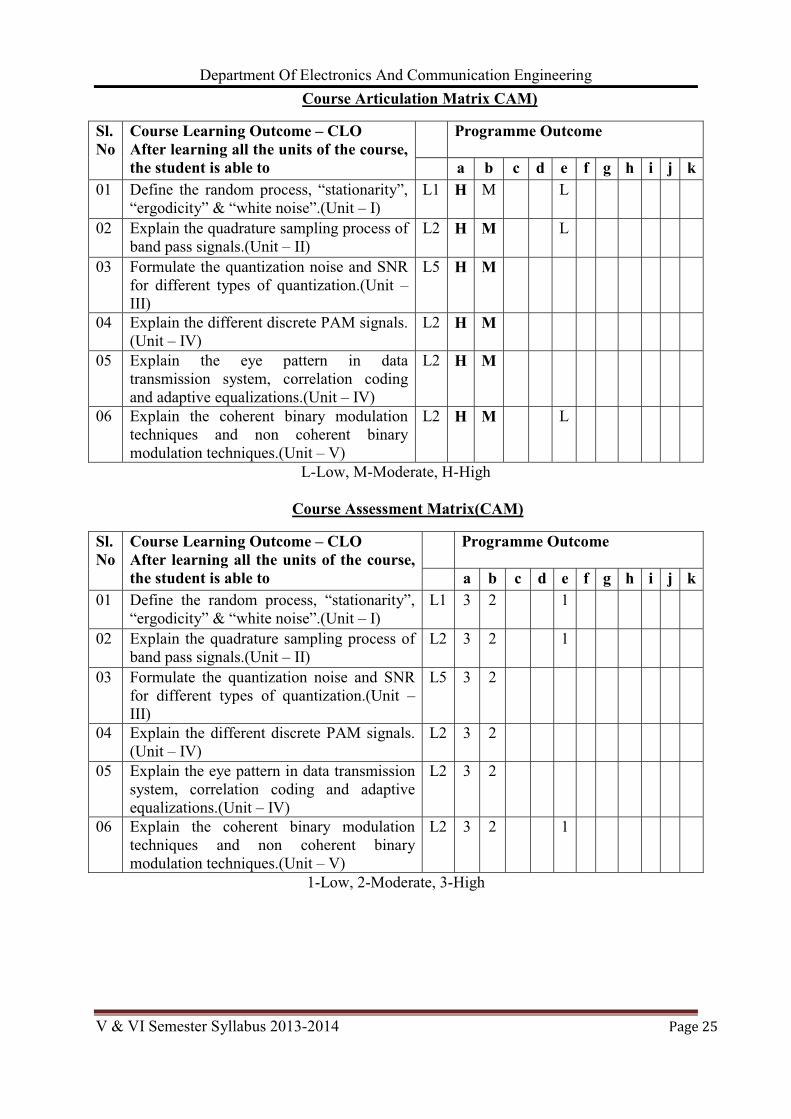
Course Outcome (CO)After learning all the units of the course, the student is able to 01 Define the random process, “stationarity”, “ergodicity” & “white noise”. – L1 (Unit – I) 02 Explain the quadrature sampling process of band pass signals. – L2 (Unit – II) 03 Formulate the quantization noise and SNR for different types of quantization. – L5 (Unit
– III) 04 Explain the different discrete PAM signals. – L2 (Unit – IV) 05 Explain the eye pattern in data transmission system, correlation coding and adaptive
equalizations. – L2 (Unit – IV) 06 Explain the coherent binary modulation techniques and non coherent binary modulation
techniques. – L2 (Unit – V)
Topic Learning OutcomesAfter learning all the topics of UNIT– I, the student is able to 01 Define the random process. – L1 02 Estimate the mean and autocorrelation function of given process. – L2 03 Define the “stationarity”, “ergodicity” and “white noise”. – L1 04 State the properties of PSD. – L1 05 Estimate the PSD of given stationary process. – L2
After learning all the topics of UNIT– II, the student is able to 01 State the meaning and implications of sampling theorem pertaining to band limited low
pass signals. – L2 02 Compare the different methods of sampling, their merits and demerits. – L4 03 Calculate the minimum sampling rate required for the signal reconstruction. – L4 04 Explain the Quadrature sampling process of band pass signals. – L2 05 Describe the natural sampling and flat–top sampling. – L2
After learning all the topics of UNIT– III, the student is able to 01 Illustrate the concept of TDM. – L3 02 Explain the block diagram of a baseband PCM system, DPCM, DM and ADM. – L3 03 Formulate the quantization noise and SNR for different types of quantization. – L5

Department Of Electronics And Communication Engineering
V & VI Semester Syllabus 2013-2014 �����������������������������������������������������������������
��
04 Explain the robust (non–uniform) quantization. – L205 Discuss the choice of appropriate step size for delta modulation. – L2 06 Define the companding of signals. – L1
After learning all the topics of UNIT– IV, the student is able to 01 Explain the different discrete PAM signals. – L2 02 Compare the PSD for binary Liv code. – L4 03 Explain the causes for occurrence of ISI. – L2 04 Explain the eye pattern in data transmission system, correlation coding and adaptive
equalizations. – L2
After learning all the topics of UNIT– V, the student is able to 01 Differentiate the digital modulation formats. – L4 02 Explain the coherent binary modulation techniques and non coherent binary modulation
techniques. – L2 03 Compare the various digital modulation schemes with reference to their probability error
and their bandwidth efficiency. – L4 04 Describe the coherent quadrature modulation techniques. – L2
Review Questions01 State the properties of PSD and also determine the PSD of given stationary process. 02 Illustrate the concept of TDM. 03 Define the random process. 04 Estimate the mean and autocorrelation function of given process. 05 Define the “stationarity”, “ergodicity” and “white noise”. 06 Sketch the block diagram of a baseband PCM system and explain. 07 Explain the causes for occurrence of ISI. 08 Describe the coherent quadrature modulation techniques. 09 Explain the causes for occurrence of ISI. 10 Explain the eye pattern in data transmission system, correlation coding and adaptive
equalizations. 11 Explain the coherent binary modulation techniques and non coherent binary modulation
techniques. 12 Compare the various digital modulation schemes with reference to their probability error
and their bandwidth efficiency. 13 Explain the block diagram of a baseband PCM system.14 Explain the block diagram of a DPCM transmitter and receiver. 15 Explain the block diagram of a DM and ADM. 16 Explain the robust (non–uniform) quantization. 17 Discuss the step size for delta modulation. 18 Define the companding of signals. 19 State and explain sampling theorem for band limited low pass signals. 20 Calculate the minimum sampling rate required for the signal reconstruction. 21 Explain the Quadrature sampling process of band pass signals. 22 Describe the natural sampling. 23 Explain flat–top sampling 24 Explain the difference between cross talk and intersymbol interference. 25 What is Quantization error? How does it depend upon the step size? 26 Explain with the help of block diagram that the Adaptive Delta modulation system
reduces the slop error at the expense of quantization error?
Department Of Electronics And Communication Engineering
V & VI Semester Syllabus 2013-2014 ����������������������������������������������������������������
��
27 Draw the wave forms comparing the response of the ADM and DM. 28 Explain the PCM technique and evaluate the expression for SNR in PCM. 29 What important functions are performed by the regenerator in PCM? 30 A voice frequency signal band limited to 3Mhz is transmitted with the use of the DM
system. The pulse repetition frequency is 30,000 pulses per second, and the step size in 40mv.determine the maximum possible speech signal amplitude to avoid a slop overload.
31 What are optimum and matched filters? Find there transfer functions? 32 Is it true that in matched filter error probability depends on signal energy and not on wave
shape? Explain. 33 To transmit a bit sequence 10011011, draw the resulting waveform using:- Unipolar RZ;
Unipolar NRZ; Bipolar RZ ; Manchester(split phase) . 34 Derive the expression for the Nyquist criterion for distortion less baseband transmission
in the absence of noise. 35 What is gram Schmitt orthogonalization procedure? Explain? 36 Explain the geometric representation of signals. 37 Explain the working of QPSK with the help of block diagram. 38 Determine the probability of error of PSK system and their required bandwidth. 39 Determine the probability of error of FSK system and their required bandwidth. 40 Derive the expression for bit error probability of a Coherent ASK system. 41 State the advantages & demerits of digital communication. 42 Draw the block diagram of digital communication system and explain. 43 Compare uniform and non-uniform quantization. 44 What is slope overload? How it is reduced? 45 List the inferences made from the eye pattern. 46 Explain µ-Law and A-Law with equations. 47 Explain concept of ideal sampling. Derive the interpolation formula. 48 Explain Maximum likely hood receiver for AWGN channel. 49 With related diagrams and equations, explain the operation of a Non-coherent receiver
using matched filter. 50 Differentiate between the transmitters of QPSK and MSK.
Lesson PlanUNIT– I
Period No. Topics
1. Introduction to Random process: 2. Random process, Random variables 3. CDF, PDF 4. CDF, PDF 5. Stastical average, Mean 6. covariance Functions 7. correlation, Properties of Auto Correlation functions 8. Properties of Auto Correlation functions 9. Power spectral density 10. Power spectral density 11. Gaussian process, Ergodicity

Department Of Electronics And Communication Engineering
V & VI Semester Syllabus 2013-2014 ����������������������������������������������������������������
��
UNIT– II Period No. Topics
12. Statement of sampling theorem, Sampling process: 13. Sampling theorem 14. Sampling theorem 15. Quadrature sampling of Band pass signals 16. Signal distortion and sampling 17. Practical aspects of sampling and signal recovery 18. Natural sampling 19. Flat top sampling 20. Flat top sampling 21. Practical Sample and Hold circuit.
UNIT– III Period No. Topics
22. Introduction to Modulation 23. PAM 24. TDM 25. PCM 26. Quantization noise 27. SNR 28. Robust quantization 29. DPCM 30. DM 31. Quantization noise in DM, ADM.
UNIT– IV Period No. Topics
32. Base– Band Shaping for Data Transmission 33. Band Shaping for Data Transmission 34. Discrete PAM signals, 35. Power spectra of discrete PAM signals. 36. Power spectra of discrete PAM signals. 37. ISI 38. Nyquist’s criterion for distortion less base– band binary transmission 39. Correlative coding 40. Eye pattern 41. Base– band M– ary PAM systems, 42. Adaptive equalization for data transmission.
UNIT– V Period No. Topics
43. Digital Modulation Techniques: 44. Digital Modulation formats 45. Digital Modulation formats 46. Coherent binary modulation techniques 47. Coherent binary modulation techniques 48. Coherent quadrature modulation techniques. 49. Coherent quadrature modulation techniques. 50. Coherent quadrature modulation techniques. 51. Non–coherent binary modulation techniques. 52. Non–coherent binary modulation technique
Department Of Electronics And Communication Engineering
V & VI Semester Syllabus 2013-2014 �����������������������������������������������������������������
��
Course Articulation Matrix CAM)
L-Low, M-Moderate, H-High
Course Assessment Matrix(CAM)
1-Low, 2-Moderate, 3-High����
Sl. No
Course Learning Outcome – CLO After learning all the units of the course, the student is able to
Programme Outcome
a b c d e f g h i j k01 Define the random process, “stationarity”,
“ergodicity” & “white noise”.(Unit – I) L1 H M L
02 Explain the quadrature sampling process of band pass signals.(Unit – II)
L2 H M L
03 Formulate the quantization noise and SNR for different types of quantization.(Unit – III)
L5 H M
04 Explain the different discrete PAM signals. (Unit – IV)
L2 H M
05 Explain the eye pattern in data transmission system, correlation coding and adaptive equalizations.(Unit – IV)
L2 H M
06 Explain the coherent binary modulation techniques and non coherent binary modulation techniques.(Unit – V)
L2 H M L
Sl. No
Course Learning Outcome – CLO After learning all the units of the course, the student is able to
Programme Outcome
a b c d e f g h i j k01 Define the random process, “stationarity”,
“ergodicity” & “white noise”.(Unit – I) L1 3 2 1
02 Explain the quadrature sampling process of band pass signals.(Unit – II)
L2 3 2 1
03 Formulate the quantization noise and SNR for different types of quantization.(Unit – III)
L5 3 2
04 Explain the different discrete PAM signals. (Unit – IV)
L2 3 2
05 Explain the eye pattern in data transmission system, correlation coding and adaptive equalizations.(Unit – IV)
L2 3 2
06 Explain the coherent binary modulation techniques and non coherent binary modulation techniques.(Unit – V)
L2 3 2 1
Department Of Electronics And Communication Engineering
V & VI Semester Syllabus 2013-2014 �����������������������������������������������������������������
��
�
Course Title : DIGITAL CMOS VLSI DESIGN Course Code: P13EC55 Semester : V L-T-P-H: 4 – 0 – 0-4 Credits:4 Contact Period : Lecture :52 Hrs., Exam: 3Hrs. Weightage :CIE:50% SEE:50%
This Course forms a prerequisite course for Low Power VLSI Design– P13EC72
Course Learning Objectives (CLOs)This Course aims to 1. Provide the basic knowledge of digital CMOS VLSI circuits and design. 2. Explain the basic electrical and physical properties of MOS transistor and dc
characteristics of MOS inverter. 3. Describe the switching characteristics and delay of MOS inverter which determines the
overall operating speed of digital systems. 4. Examine the static and dynamic characteristics of various combinational MOS logic
circuits and sequential logic circuits. 5. Discuss the operation of dynamic logic circuits of reduced circuit delay and silicon area,
compared to static logic circuits. 6. Discuss the static and dynamic behaviour of BICMOS circuits and some of its
applications. 7. Provide the knowledge of I/O circuits, clock generation and distribution circuits which
are essential in VLSI design chip. Course Content
UNIT – I MOS Transistor : The Metal Oxide Semiconductor(MOS) Structure, The MOS System under External Bias, Structure and Operation of MOS Transistor (MOSFET), MOSFET Current – Voltage Characteristics, MOSFET Scaling and Small – Geometry Effects, MOSFET Capacitances MOS Inverters, Static Characteristics: Introduction, Resistive – Load Inverter, Inverters with n– Type MOSFET Load, CMOS Inverter Text: – 3.1 to 3.6, 5.1 to 5.4 10 Hrs
UNIT – II MOS Inverters: Switching Characteristics and Interconnect Effects: Introduction, Delay – Time Definitions, Calculation of Delay Times, Inverter Design with Delay Times, Estimation of Interconnect Parasitic, Calculation of Interconnect Delay, Switching Power Dissipation of CMOS Inverters Text: – 6.1 to 6.7 10 Hrs
UNIT – III Combinational MOS Logic Circuits : Introduction, MOS Logic Circuits with Depletion nMOS Loads, CMOS Logic Circuits, Complex Logic Circuits, CMOS Transmission Gates(Pass Gates) Sequential MOS Logic Circuits : Introduction, Behavior of Bistable Elements, SR Latch Circuit, Clocked Latch and Flip– Flop Circuits, CMOS D– Latch and Edge – Triggered Flip– Flop Text: – 7.1 to 7.5, 8.1 to 8.5 11 Hrs
UNIT – IV Dynamic Logic Circuits: Introduction, Basic Principles of Pass Transistor Circuits, Voltage Bootstrapping, Synchronous Dynamic Circuit Techniques, Dynamic CMOS Circuit Techniques, High– Performance Dynamic CMOS CircuitsText: – 9.1 to 9.6 10 Hrs
Department Of Electronics And Communication Engineering
V & VI Semester Syllabus 2013-2014 ��������������������������������������������������������������� �
��
UNIT – V BiCMOS Logic Circuits: Introduction, Bipolar Junction Transistor (BJT): Structure and Operation, Dynamic Behavior of BJTs, Basic BiCMOS Circuits: Static Behavior, Switching Delay in BiCMOS Logic Circuits, BiCMOS ApplicationsChip Input and Output (I/O) Circuits: Introduction, ESD Protection, Input Circuits, Output Circuits and L (di/dt) Noise, On– Chip Clock Generation and Distribution, Latch – Up and Its Prevention Text: – 12.1 to 12.6, 13.1 to 13.6 11 Hrs
TEXT BOOK: “CMOS Digital Integrated Circuits Analysis and Design”, Sung – Mo Kang, Yusuf Leblebici, Third Edition, Tata McGrawhill
REFERENCE BOOKS: 1. “Introduction to VLSI Circuits and systems”, John .P. Uyemura, John Wiley, 3rd edition
2002 2. “Principles of CMOS VLSI Design”, Neil. H. E. Weste, Kamran Eshraghian, 2nd edition
2002. 3. “Basic VLSI Design”, Douglas A. Pucknell, Kamran Eshraghian, 3rd Edition 2006.
Course OutcomeAfter learning all the units of the course, the student is able to 01 Explain the structure, operation and characteristics of MOSFET, the scaling, small
geometry effects and capacitance of MOSFET. – L2 (Unit – I) 02 Analyze the switching characteristics, delay time definitions, interconnect delay and
parasitic of MOS inverter, the switching power dissipation with respect to MOS inverters. – L4 (Unit – II)
03 Analyze the combinational and sequential MOS and CMOS logic circuits, transmission gates, latches and flipflops. – L4 (Unit – III)
04 Discuss the principles of pass transistor circuits and the working of different dynamic logic circuit techniques, dynamic CMOS circuit techniques and high–performance dynamic CMOS circuits – L2 (Unit – IV)
05 Explain the structure and operation of dynamic and static behaviour of BJT’s and BICMOS logic. – L2 (Unit – V)
06 Analyze the chip I/O circuit, noise effect, on chip clock generation and distribution circuits. – L4 (Unit – V)
Topic Learning OutcomeAfter learning all the topics of UNIT– I, the student is able to 01 Explain the structure of MOS transistor and threshold voltage. – L2 02 Describe the operation, V– I characteristics, voltage current equation, gradual channel
approximation, channel length modulation, Substrate bias effect of MOS transistor. – L2 03 Discuss the measurement of parameter of MOSFETS. – L2 04 Explain the MOSFETS scaling and small geometry effects. – L2 05 Discuss the effects of different MOSFET’s capacitances. – L2 06 Describe the voltage transfer characteristics, noise immunity and noise margin, power and
area consideration of NMOS inverter. – L2 07 Analyze the drain current, output low voltage, output high voltage, noise margin, power
consumption and chip area of resistive load inverter. – L4 08 Discuss the inverter with N type MOS FETS load such as enhancement load NMOS
inverter, depletion load NMOS inverter. – L2

Department Of Electronics And Communication Engineering
V & VI Semester Syllabus 2013-2014 �����������������������������������������������������������������
��
09 Calculate the VOH, VOL, VIL, and VIH for depletion load NMOS inverter circuit. – L4 10 Explain the circuit operation, supply voltage scaling, power and area consideration of
CMOS inverter. – L2 11 Calculate the VIL, VIH, VTH of CMOS inverter. – L4
After learning all the topics of UNIT– II, the student is able to 01 Explain the delay time definition, calculation of delay times of CMOS inverter. – L2 02 Discuss the design of CMOS inverter with delay constants. – L2 03 Describe the effects of interconnect parasitic, interconnect capacitance estimation and
resistance estimation. – L2 04 Analyze the interconnect delay with RC delay models, Elmore delay. – L4 05 Explain the switching power dissipation and power delay product of CMOS inverter. – L2 06 Solve the numerical problem on CMOS inverter design. – L3
After learning all the topics of UNIT– III, the student is able to 01 Describe the working of MOS logic circuits with depletion NMOS loads , calculation of
Voh , Vol. – L2 02 Explain the structure of two inputs, multiple input NOR gate and NAND gate. – L2 03 Discuss the transient neither analyze of NOR gate and NAND gate. – L2 04 Analyze the CMOS nor to and CMOS NAND two gate. – L4 05 Calculate the switching threshold voltage neither for CMOS nor to and CMOS NAND
two gates. – L4 06 Explain the circuit and layout of complex CMOS logic gates. – L2 07 Analyze the pseudo NMOS gate, CMOS full adder circuit. – L4 08 Describe the circuit and working of transmission gates, complementary pass transistor
logic. – L2
After learning all the topics of UNIT– IV, the student is able to 01 Explain the basic principles of pass transistor circuits, charge storage and charge leakage.
– L2 02 Describe the voltage bootstrapping methods. – L2 03 Discuss the synchronous dynamic circuit techniques with dynamic pass transistors
circuits. – L2 04 Explain the dynamic MOS circuit techniques with CMOS transmission gate logic. – L2 05 Discuss the high performance dynamic CMOS such as dominos CMOS logic, NORA
CMOS logic, Zipper CMOS circuit, true single phase clock dynamic CMOS. – L2
After learning all the topics of UNIT– V, the student is able to 01 Explain the structure, operation VI models of BJT. – L2 02 Describe the BJT inverter circuit, static characteristics and dynamic behaviour with
charge control model. – L2 03 Discuss the basic BiCMOS circuits, static behaviour, switching delay and BiCMOS
application - L2 04 Explain the ESD protection, input circuit, output circuit and L [di/dt] noise. – L2 05 Discuss the different on chip clock generation and distribution methods. – L2 06 Explain the latch up problems in CMOS chip and its prevention techniques. – L2

Department Of Electronics And Communication Engineering
V & VI Semester Syllabus 2013-2014 �����������������������������������������������������������������
��
Review questions1. With neat diagram explain the structure and working of MOS transistor. 2. Explain the MOS system under external bias and body bias effect. 3. Describe the operation and V– I characteristics of MOSFET 4. Derive the voltage current equation of MOSFET 5. Explain gradual channel approximation and channel length modulation of
MOSFET 6. Explain the measurement of parameter of MOSFETS. 7. Explain the MOSFETS scaling and small geometry effects. 8. Discuss the short channel effect and narrow channel effect of MOSFET 9. Discuss the effects of different MOSFET’s capacitances. 10. Draw the circuit of NMOS inverter and explain its voltage transfer characteristics 11. Describe the noise immunity and noise margin of NMOS inverter. 12. Discuss power and area consideration of NMOS inverter. 13. Analyze the drain current, output low voltage, output high voltage and noise margin
of NMOS inverter. 14. Explain power consumption and chip area of resistive load inverter. 15. Discuss the inverter with N type MOSFETS enhancement load NMOS inverter 16. Discuss the inverter with N type MOSFETS depletion load NMOS inverter. 17. Calculate the VOH, VOL, VIL, and VIH for depletion load NMOS inverter circuit. 18. Explain the circuit operation, supply voltage scaling of cmos inverter. 19. Discuss power and area consideration of CMOS inverter. 20. Calculate the VIL, VIH, VTH of CMOS inverter. 21. Explain the delay time definition of CMOS inverter.22. Calculate the total delay times of CMOS inverter. 23. Analyse the design of CMOS inverter with delay constants. 24. Discuss the effects of interconnect parasitic capacitance and resistance 25. Explain the estimation of interconnect capacitance and resistance. 26. Analyze the interconnect delay with RC delay models, Elmore delay. 27. Explain the switching power dissipation and power delay product of CMOS inverter. 28. Describe the working of MOS logic circuits with depletion NMOS loads 29. Calculate Voh and Vol of logic circuits with depletion NMOS loads 30. Explain the structure of two inputs , multiple input NAND gate and NOR gate. 31. Discuss the transient analysis of NOR gate and NAND gate. 32. Analyze the CMOS NOR2 gate and CMOS NAND2 gate. 33. Calculate the switching threshold voltage for CMOS NOR2 gate. 34. Calculate the switching threshold voltage for CMOS NAND2 gates. 35. Explain the circuit and layout of complex CMOS logic gates. 36. Analyze the pseudo NMOS gate and CMOS full adder circuit. 37. Describe the circuit and working of transmission gates 38. Describe the circuit and working of complementary pass transistor logic. 39. Explain the basic principles of pass transistor circuits, charge storage and charge
leakage. 40. Describe the voltage bootstrapping methods. 41. Discuss the synchronous dynamic circuit techniques with dynamic pass transistors
circuits. 42. Explain the dynamic MOS circuit techniques with CMOS transmission gate logic. 43. Discuss the high performance dynamic dominos CMOS logic. 44. Explain NORA CMOS logic, Zipper CMOS circuit and true single phase clock
dynamic CMOS.
Department Of Electronics And Communication Engineering
V & VI Semester Syllabus 2013-2014 ����������������������������������������������������������������
��
45. Explain the structure, operation VI models of BJT. 46. Describe the BJT inverter circuit, static characteristics and dynamic behaviour with
charge control model. 47. Discuss the basic BiCMOS circuits, static behaviour, switching delay and BiCMOS
application. 48. Explain the ESD protection, input circuit, output circuit and L [di/dt] noise. 49. Discuss the different on chip clock generation and distribution methods. 50. Explain the latch up problems in CMOS chip and its prevention techniques.
Lesson planUNIT – I
Period No. Topics 1. MOS Transistor : introduction The Metal Oxide Semiconductor(MOS) Structure2. The MOS System under External Bias 3. Structure and Operation of MOS Transistor (MOSFET) 4. MOSFET Current – Voltage Characteristics 5. MOSFET Scaling and Small – Geometry Effects, 6. MOSFET Capacitances 7. MOS Inverters, Static Characteristics: Introduction, Resistive – Load Inverter 8. Inverters with n– Type MOSFET Load 9. CMOS Inverter
10. examplesUNIT – II
Period No. Topics 1. MOS Inverters: Switching Characteristics and Interconnect Effects: Introduction, Delay 2. Time Definitions, Calculation of Delay Times 3. Inverter Design with Delay Times 4. Estimation of Interconnect Parasitic 5. Calculation of Interconnect Delay 6. Calculation of Interconnect Delay 7. Switching Power Dissipation of CMOS Inverters 8. Switching Power Dissipation of CMOS Inverters 9. Examples
10. Examples UNIT – III
Period No. Topics 1. Combinational MOS Logic Circuits : Introduction, MOS Logic Circuits with Depletion
nMOS Loads 2. CMOS Logic Circuits 3. Complex Logic Circuits 4. CMOS Transmission Gates(Pass Gates) 5. Sequential MOS Logic Circuits : Introduction 6. Behavior of Bistable Elements, SR Latch Circuit 7. Clocked Latch and Flip– Flop Circuits, 8. CMOS D– Latch and Edge – Triggered Flip– Flop 9. CMOS D– Latch and Edge – Triggered Flip– Flop
10. Examples 11. Examples

Department Of Electronics And Communication Engineering
V & VI Semester Syllabus 2013-2014 ����������������������������������������������������������������
��
UNIT – IV Period No. Topics 1. Dynamic Logic Circuits: Introduction 2. Basic Principles of Pass Transistor Circuits 3. Basic Principles of Pass Transistor Circuits 4. Voltage Bootstrapping 5. Synchronous Dynamic Circuit Techniques 6. Dynamic CMOS Circuit Techniques 7. Dynamic CMOS Circuit Techniques 8. High– Performance Dynamic CMOS Circuits 9. Examples
10. Examples
UNIT – V Period No. Topics 1. BiCMOS Logic Circuits: Introduction 2. Bipolar Junction Transistor (BJT): Structure and Operation 3. Dynamic Behavior of BJTs 4. Basic BiCMOS Circuits: Static Behavior 5. Switching Delay in BiCMOS Logic Circuits 6. BiCMOS Applications 7. Chip Input and Output (I/O) Circuits: Introduction 8. ESD Protection, Input Circuits 9. Output Circuits and L (di/dt) Noise
10. On– Chip Clock Generation and Distribution 11. Latch – Up and Its Prevention

Department Of Electronics And Communication Engineering
V & VI Semester Syllabus 2013-2014 ����������������������������������������������������������������
��
�
Course Articulation Matrix(CAM)
Sl. No
Course Learning Outcome – CLO After learning all the units of the course, the student is able to
Programme outcome
a b c d e f g h i j k01 Explain the structure, operation and characteristics of
MOSFET, the scaling, small geometry effects and capacitance of MOSFET. – L2 (Unit – I)
M M L
02 Analyze the switching characteristics, delay time definitions, interconnect delay and parasitic of MOS inverter, the switching power dissipation with respect to MOS inverters. – L4 (Unit – II)
M
03 Analyze the combinational and sequential MOS and CMOS logic circuits, transmission gates, latches and flipflops. – L4 (Unit – III)
M L
04 Discuss the principles of pass transistor circuits and the working of different dynamic logic circuit techniques, dynamic CMOS circuit techniques and high–performance dynamic CMOS circuits – L2 (Unit – IV)
M
05 Explain the structure and operation of dynamic and static behaviour of BJT’s and BICMOS logic. – L2 (Unit – V) M L L
06 Analyze the chip I/O circuit, noise effect, on chip clock generation and distribution circuits. – L4 (Unit – V) M L
L-Low, M-Moderate, H-High Course Assessment Matrix(CAM)
Sl. No
Course Learning Outcome – CLO After learning all the units of the course, the student is able to
Programme outcome
a b c d e f g h i j k01 Explain the structure, operation and characteristics of
MOSFET, the scaling, small geometry effects and capacitance of MOSFET. – L2 (Unit – I)
2 2 1
02 Analyze the switching characteristics, delay time definitions, interconnect delay and parasitic of MOS inverter, the switching power dissipation with respect to MOS inverters. – L4 (Unit – II)
2
03 Analyze the combinational and sequential MOS and CMOS logic circuits, transmission gates, latches and flipflops. – L4 (Unit – III)
2 1
04 Discuss the principles of pass transistor circuits and the working of different dynamic logic circuit techniques, dynamic CMOS circuit techniques and high–performance dynamic CMOS circuits – L2 (Unit – IV)
2
05 Explain the structure and operation of dynamic and static behaviour of BJT’s and BICMOS logic. – L2 (Unit – V)
2 1 1
06 Analyze the chip I/O circuit, noise effect, on chip clock generation and distribution circuits. – L4 (Unit – V) 2 1
1-Low, 2-Moderate, 3-High

Department Of Electronics And Communication Engineering
V & VI Semester Syllabus 2013-2014 ���������������������������������������������������������������
��
Course Title : OPTICAL COMMUNICATION SYSTEMS Course Code: P13EC56 Semester : V L-T-P-H: 4 – 0 – 0-4 Credits:4 Contact Period : Lecture :52 Hrs., Exam: 3Hrs. Weightage :CIE:50% SEE:50%
Course Learning Objectives (CLOs)This course aims to 1. Discuss the types, characteristics, constitution and application of optical fibers. 2. Describe the propagation of light waves through the fibers. 3. State the causes for the absorption mechanisms in fibers. 4. Explain the bending losses in fibers. 5. Discuss the construction and operation of optical sources. 6. List the different lensing schemes for coupling improvement. 7. Outline the physical principles of photodiodes. 8. Explain the digital link and analog link. 9. Discuss the WDM concepts and components. 10. Describe the optical amplifiers and optical networks.
Course ContentUNIT – I
Optical Fibers: Structures, Wave guiding. Basics optical laws and definitions, optical fiber modes and configurations, mode theory for circular waveguides, single–mode fibers, graded index fiber structure, fiber materials, photonic crystal fibers, fiber fabrication, Attenuation, signal distortion in fibers. Text: 2.2 to 2.9, 3.1to 3.2 10 Hrs
UNIT – II Optical Sources: Topics from semiconductor physics, Light–Emitting Diodes (LEDs), Laser Diodes.Power Launching and coupling: Source to fiber power launching, lensing schemes for coupling improvement, fiber to fiber joints, LED coupling to single mode fibers, fiber splicing. Text: 4.1 to 4.3, 5.1 to 5.5 10 Hrs
UNIT – III Photo Detectors: Physical principles of photodiodes, photo detector noise, detector response time.Optical Receiver Operation: Fundamental receiver operation, digital receiver performance, eye diagrams, burst mode receivers, analog receivers. Text: 6.1 to 6.3, 7.1 to 7.5 10 Hrs
UNIT – IV Digital Links: Point to point link.Analog Links: Overview of analog links, carrier to noise ratio, multichannel transmission techniques, RF over fiber, radio over fiber links. WDM Concepts and Components: Overview of WDM, passive optical couplers, isolators and circulators, fiber grating filters. Text: 8.1, 9.1 to 9.5, 10.1 to 10.4 11 Hrs
UNIT – V Optical Amplifiers: Basic applications and types of optical amplifiers, semiconductor optical amplifiers, erbium– doped fiber amplifiers.Optical Networks: Network concepts, network topologies, SONET/SDH, High speed light wave links, optical add/drop multiplexing, optical switching, WDM network examples.
Department Of Electronics And Communication Engineering
V & VI Semester Syllabus 2013-2014 ���������������������������������������������������������������
��
Text: 11.1 to 11.3, 13.1 to 13.7 11 Hrs
TEXT BOOK: “Optical Fiber Communications”, Gerd Keiser, McGraw Hill, 5th Edition–2013
REFERENCE BOOKS: 1. “Optical Fiber Communications”, John M. Senior, Pearson Education 2nd Edition 2. “Fiber Optic Communication”, Joseph Palais, Pearson Education, 4th Edition 3. “Optical Communication Systems”, Satinder Bal Gupta, Ashish Goel, University
Science Press, New Delhi. Course Outcome
After learning all the units of the course, the student is able to 01 Develop the wave equations for step index fiber. – L5 (Unit – I) 02 Develop the expressions for quantum efficiency and emitted optical power in LED. – L5
(Unit – II) 03 Explain the operation of a pin photo diode circuit with an applied reverse bias. – L2 (Unit
– III) 04 Calculate the optical link power budget in optical communication line. – L4 (Unit – IV) 05 Explain the basic constituents of a generic RF over fiber link. – L2 (Unit – IV) 06 Describe the wave guide coupler, erbium doped fiber amplifier and SONET/SDH
networks. – L2 (Unit – V)
Topic Learning Outcome After learning all the topics of UNIT– I, the student is able to 01 Define the snell’s law. – L1 02 Calculate the critical angle for the light travelling in the glass. – L4 03 Describe the polarization – sensitive materials with examples. – L1 04 Distinguish between the step index fiber and graded index fiber, as well as single mode
fiber and multimode fiber. – L2 05 Develop the necessary condition that angle of incidence should satisfy, for the light way
to propagate in the dielectric slab waveguide. – L506 Differentiate the meridional rays and skew rays. – L4 07 Explain the significance of cutoff wavelength and V– number for light propagation in the
waveguide. – L2 08 Apply the Maxwell’s equations to cylindrical system to obtain waveguide equations. – L2 09 Discuss the modes of propagation in step index fibers, with the sketches. – L2 10 Sketch the schematic of a fiber drawing operators. – L3 11 Calculate the ultra violet absorptions at different wavelengths. – L4 12 Discuss the micro bending and macro bending losses in optical fibers. – L2 13 List the causes of intra model dispersion. – L1
After learning all the topics of UNIT– II, the student is able to 01 Sketch the cross sectional drawing of a double hetero structure light emitter type of LED.
– L3 02 Develop the expression for the optical power generated internally to the LED, the optical
power emitted from the LED and quantum efficiency. – L5 03 Discuss the processes of absorption, spontaneous emission and stimulated emission in
laser diodes. – L2
Department Of Electronics And Communication Engineering
V & VI Semester Syllabus 2013-2014 ����������������������������������������������������������������
��
04 Develop the expression for the number of photons per unit volume emitted by the laser and for the external quantum efficiency of the laser. – L5
05 Sketch the radiance patterns for a lambertian source and the lateral output of a highly directional laser diode. – L3
06 Explain the different lensing schemes to improve optical source to fiber coupling efficiency. – L2
07 Calculate the insertion loss at the two fiber joints and the power coupling at the joints. – L4
08 Discuss the steps involved in fiber end face preparation. – L2 09 List the common end face defects during fiber end preparation. – L1 10 Explain the different splicing techniques. – L2
After learning all the topics of UNIT– III, the student is able to 01 Sketch the pin photodiode circuits with the reverse bias and the corresponding energy
band diagram. – L3 02 Compare the responsivity and quantum efficiency for the pin diodes of three different
materials. – L4 03 Show the construction of reach through avalanche photodiode along with the electric field
variation in depletion and multiplication regions. – L3 04 Discuss the importance of noise sources and signal to noise ration in photo detector. – L2 05 Develop the relationship for the total current density through the reverse biased depletion
layer of pin photodiode. – L5 06 Discuss the factors contributing towards the response time of a photodiode with output
circuits. – L2 07 Show the signal path through an optical data link for digital signal transmission in a block
diagram. – L3 08 List the noise sources and disturbances in an optical pulse detection mechanism. – L1 09 Discuss the operations of high impedance amplifier and trans– impedance amplifier. – L2 10 List the different information’s which can be obtained from the eye pattern. – L1 11 Show the architecture of a typical passive optical network. – L3
After learning all the topics of UNIT– IV, the student is able to 01 Discuss the losses that occur at each element of the point– to– point digital link between a
transmitter and a receiver. – L2 02 Develop the relationship for the total system rise time of an optical digital link in terms of
transmitter rise time, the group velocity dispersion rise time, the modal dispersion rise time and the receiver rise time. . – L5
03 List the major noise contributors in an analog link. – L1 04 Explain how sub carrier multiplexing is adopted to transmit both analog and digital
signals simultaneously. –L2 05 Describe the basic constituents of a generic R.F.–over–fiber link to transmit microwave
analog signals. – L1 06 Discuss the Rader–over fiber, concept of a broad band wireless access network for
interconnecting Antenna base station with the central controlling office. – L2 07 Show the implementation of a typical WDM network containing different optical
amplifiers. – L3 08 Explain the fused – fiber coupler with a coupling region and two tapered regions. – L2 09 Calculate the coupling length of a symmetric waveguide coupler of a fixed coupling
efficient for complete power transfer. – L4 10 Describe the design and operation of a polarization –independent isolator. – L1
Department Of Electronics And Communication Engineering
V & VI Semester Syllabus 2013-2014 ����������������������������������������������������������������
��
11 Explain the operational concept of a three –port circulator. – L2 12 Outline the concept of de–multiplexing function using a fiber grating and an optical
circulator. – L1
After learning all the topics of UNIT– V, the student is able to
01 Sketch the four possible applications of three classes of optical amplifiers, namely in line optical amplifier, Pre–amplifier, power amplifier. – L3
02 List the various amplifier structures and their operating regions. – L1 03 Calculate the photon density in semiconductor optical amplifier with the given
specifications. – L4 04 Sketch the simplified energy – level diagrams and the transaction processes of Er ions in
silica of erbium–doped fiber amplifier. – L3 05 Calculate the maximum input power and maximum output power for EDFA with given
specification. – L4 06 Discuss the common topologies used for fiber optic networks. – L2 07 Explain the losses encountered in a passive linear bus coupler consisting of two
directional couplers in cascade. – L2 08 Develop the power–balance equation for a particular link between two stations in a star
network. – L5. 09 Sketch the basic formats of an STS–N SONET frame and an STM–N SDH frame. – L3 10 Explain the generic two–fiber unidirectional path– switched ring (UPSR) with a counter–
rotating protection path. – L2 11 Sketch the ultra fast point–to–point transmission system using optical TDM. – L3 12 Explain the optical cross–connect architecture using optical space switches and no
wavelength Converters. – L2.
Review Questions:01 Explain the propagation of meridonal and skew rays along the fiber. 02 Compare step-index fiber with graded index fiber with respect to construction,
performance and application. 03 With a neat schematic explain the structure of conventional fiber. 04 List out the types of fiber with respect to its refractive indices and modes. 05 What is numerical aperture? Derive an expression for numerical aperture and acceptance
angle in case of step-index fiber. 06 List any four types of fiber fabrication process. Explain OVPO process with schematic. 07 What is attenuation? Mention the types of attenuation in fiber and give the relation for
attenuation. 08 Write a short note on: (a) Refractive index, Reflection and refraction
(b) Polarisation sensitive materials (c) fiber materials
09 Sketch and explain the structure of high impedance and trans impedance amplifiers. 10 Explain briefly the fundamental concepts of a coherent light wave system with necessary
sketch. 11 Mention the necessary condition that an optical wave incident at angle
should satisfy in dielectric wave guide propagation and derive it. 12 Discuss the power flow concepts in step-index fibers. 13 Explain the extrinsic and intrinsic absorption mechanism in optical fibers. 14 Write a note on fiber-drawing apparatus.
Department Of Electronics And Communication Engineering
V & VI Semester Syllabus 2013-2014 �������������������������������������������������������������� �
��
15 Explain the different lensing schemes used improve the coupling efficiency between optical source and the fiber.
16 Discuss the joint losses due to mismatch in core diagram, numerical aperture and core refractive index profile.
17 How are the fiber ends prepared under control fracture procedure?. Describe with the figure.
18 Mention the principle requirements of good connector design. 19 Starting from the fundamental concepts, derive the expression for the responsivity of pin
photo diode. 20 Estimate the number of modes and V– number for a given fiber. 21 Develop the wave equations for step index fiber. 22 Sketch the transverse electric field vectors in step index fiber. 23 Sketch the cross section diagram of a double hetero structure light emitter. 24 Develop the expressions for quantum efficiency and emitted optical power in LED. 25 Explain the construction and operation on Fabry perot resonator cavity laser. Calculate
the power coupled into step index or graded index fiber from LED. 26 Explain the operation of a pin photo diode circuit with an applied reverse bias. Calculate
the quantum efficiency & responsibility of pin photo diode. 27 Discuss the factors contributing to the response time of photodiode. 28 List the sources of error in optical pulse detection mechanism. 29 Calculate the optical link power budget in optical communication line for given
specification. 30 Define the relative refractive index difference for an optical fiber and show how it may be
related to numerical aperture. 31 Outline the common LED structures for OFC discussing their relative merits and
drawbacks. 32 Discuss lens coupling of LEDs to optical fibers and outline the various techniques
employed. 33 What is meant by fusion splicing of OF. Discuss the advantages and drawbacks of this
jointing techniques. 34 With aid of suitable diagrams describes three common techniques use for mechanical
splicing of Optical Fibers. 35 Compare the relative advantages and disadvantages of LED and laser diode. 36 Discuss OF cable design with regards to fiber buffering. 37 Explain SONET-SDH with a neat diagram. 38 Explain the operational principles of WDM. 39 With the aid of simple sketches outline the major categories of multiport OF coupler. 40 Describe two common methods use in the fabrication of three and four fiber couplers. 41 Outline the three major categories of passive WDM coupler. 42 Illustrate the architecture of a typical passive optical network(PON). 43 With neat diagrams explain the fundamental measurement parameters of eye pattern. 44 Explain the construction and working of erbium– doped fiber amplifiers. 45 Discuss the homodyne detection and heterodyne detection. 46 Explain the simplex point to point link with a neat sketch. 47 Explain optical add/drop multiplexing. 48 Sketch the basic format of an STS-N SONET frame and an STM-N SDH frame.

Department Of Electronics And Communication Engineering
V & VI Semester Syllabus 2013-2014 ����������������������������������������������������������������
��
Lesson Plan:UNIT – I
Period No. Topics 1. Optical Fibers: Structures, Waveguiding. 2. Basics optical laws and definitions. 3. Optical fiber modes and configurations. 4. Mode theory for circular waveguides. 5. Single–mode fibers. 6. Graded index fiber structure. 7. Fiber materials. 8. Photonic crystal fibers. 9. Fiber fabrication, Attenuation. 10. Signal distortion in fibers.
UNIT – II Period No. Topics
11. Optical Sources: Topics from semiconductor physics 12. Light–Emitting Diodes (LEDs). 13. Light–Emitting Diodes (LEDs). 14. Laser Diodes. 15. Power Launching and coupling: Source to fiber power launching. 16. Source to fiber power launching. 17. Lensing schemes for coupling improvement. 18. fiber to fiber joints. 19. LED coupling to single mode fibers. 20. fiber splicing.
UNIT – III Period No. Topics
21. Photo Detectors: Physical principles of photodiodes. 22. Photo detector noise. 23. Photo detector noise. 24. Detector response time. 25. Optical Receiver Operation: Fundamental receiver operation. 26. Digital receiver performance. 27. Eye diagrams. 28. Eye diagrams. 29. Burst mode receivers. 30. Analog receivers.
UNIT – IV Period No. Topics
31. Digital Links: Point to point link. 32. Point to point link. 33. Analog Links: Overview of analog links. 34. Carrier to noise ratio. 35. Multichannel transmission techniques. 36. RF over fiber. 37. Radio over fiber links. 38. WDM Concepts and Components: Overview of WDM. 39. Passive optical couplers. 40. Isolators and circulators. 41. Fiber grating filters.
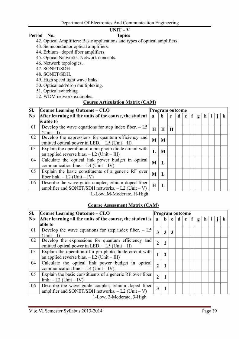
Department Of Electronics And Communication Engineering
V & VI Semester Syllabus 2013-2014 ����������������������������������������������������������������
��
UNIT – V Period No. Topics
42. Optical Amplifiers: Basic applications and types of optical amplifiers. 43. Semiconductor optical amplifiers. 44. Erbium– doped fiber amplifiers. 45. Optical Networks: Network concepts. 46. Network topologies. 47. SONET/SDH. 48. SONET/SDH. 49. High speed light wave links. 50. Optical add/drop multiplexing. 51. Optical switching. 52. WDM network examples.
Course Articulation Matrix (CAM)
L-Low, M-Moderate, H-High
Course Assessment Matrix (CAM)
1-Low, 2-Moderate, 3-High
Sl. No
Course Learning Outcome – CLO After learning all the units of the course, the student is able to
Program outcomea b c d e f g h i j k
01 Develop the wave equations for step index fiber. – L5 (Unit – I)
H H H 02 Develop the expressions for quantum efficiency and
emitted optical power in LED. – L5 (Unit – II) M M
03 Explain the operation of a pin photo diode circuit with an applied reverse bias. – L2 (Unit – III) L M
04 Calculate the optical link power budget in optical communication line. – L4 (Unit – IV) M L
05 Explain the basic constituents of a generic RF over fiber link. – L2 (Unit – IV) M L
06 Describe the wave guide coupler, erbium doped fiber amplifier and SONET/SDH networks. – L2 (Unit – V) H L
Sl. No
Course Learning Outcome – CLO After learning all the units of the course, the student is able to
Program outcomea b c d e f g h i j k
01 Develop the wave equations for step index fiber. – L5 (Unit – I)
3 3 3 02 Develop the expressions for quantum efficiency and
emitted optical power in LED. – L5 (Unit – II) 2 2
03 Explain the operation of a pin photo diode circuit with an applied reverse bias. – L2 (Unit – III) 1 2
04 Calculate the optical link power budget in optical communication line. – L4 (Unit – IV) 2 1
05 Explain the basic constituents of a generic RF over fiber link. – L2 (Unit – IV) 2 1
06 Describe the wave guide coupler, erbium doped fiber amplifier and SONET/SDH networks. – L2 (Unit – V) 3 1
Department Of Electronics And Communication Engineering
V & VI Semester Syllabus 2013-2014 ����������������������������������������������������������������
��
Course Title : DIGITAL SIGNAL PROCESSING LABORATORYCourse Code: P13ECL57 Semester : V L-T-P-H:0 – 0 – 3-3 Credits:1.5 Contact Period : Lecture :39 Hrs, Exam: 3Hrs. Weightage :CIE:50% SEE:50%
Course Learning Objectives (CLOs)This course aims to 1. Provide the basic knowledge of how to use MATLAB for DSP concepts. 2. Illustrate the Verification of sampling theorem. 3. Identify the Impulse response of a given system. 4. Provide the Linear convolution of two given sequences. 5. Compute the Circular convolution of two given sequences. 6. Identify the Autocorrelation of a given sequence and verification of its properties. 7. Compute the Cross correlation of given sequences and verification of its properties. 8. Solve the given difference equation. 9. Compute the N point DFT of a given sequence and to plot magnitude and phase spectrum. 10. Demonstrate the Linear convolution of two sequences using DFT and IDFT. 11. Compute the Circular convolution of two given sequences using DFT and IDFT. 12. Design the FIR filter to meet the given specifications. 13. Design the IIR filter to meet the given specifications. 14. Predict the Linear convolution of two given sequences. 15. Produce the Circular convolution of two given sequences. 16. Compute the N Point DFT of a given sequence. 17. Realize the FIR filter to meet the given specifications for the input signal from function
generator / speech signal. 18. Obtain the Impulse response of first order and second order system.
Course ContentA. EXPERIMENTS USING MATLAB / SCILAB / OCTAVE / WAB
01 Introduction to MATLAB and Verification of the sampling theorem. 02 Determination of Impulse response of the given system and solution of Difference
equation for the same system. 03 Linear convolution of the two given sequences using shortcut methods, DFT and IDFT. 04 Circular convolution of the two given sequences using shortcut methods, DFT and IDFT. 05 Autocorrelation of the given sequence and verification of its properties. 06 Cross correlation of the given sequences and verification of its properties. 07 Computation of the N point DFT of a given sequence and to plot magnitude and phase
spectrum. 08 Design and implementation of the FIR filter to meet the given specifications (Hamming,
Hanning, Rectangular & Kaiser windows). 09 Design and implementation of the IIR filter to meet the given specifications (Butterworth
and Chebyshev Type-I & Type-II).
B. EXPERIMENTS USING DIGITAL SIGNAL PROCESSOR (TMS320C54XX) AND CODE COMPOSER STUDIO (CCS)
(Note: Experiments no. 1, 2, 3 & 4 may be performed on CCS) 01 Determine the Linear and Circular convolution of the two given sequences. 02 Computation of the N Point DFT and IDFT of a given sequence. 03 Determination of Impulse response of first order and second order system.
Department Of Electronics And Communication Engineering
V & VI Semester Syllabus 2013-2014 ����������������������������������������������������������������
��
04 Realizations of the FIR filter to meet given specifications. The input can be a signal from function generator / speech signal.
REFERENCE BOOKS: 1. “Digital signal processing using MATLAB”, Sanjit K Mitra, TMH, 2001 2. “Digital signal processing using MATLAB”, J.G. Proakis & Ingle, MGH, 2000 3. ”Digital signal processors”, B.Venkataramani and Bhaskar, TMH,2002
Course Outcome After conducting all the experiments the student is able to 01 Demonstrate the Verification of sampling theorem. – L3 02 Generate the Impulse response of a given system. – L5 03 Calculate the Linear convolution of two given sequences. – L4 04 Compute the Circular convolution of two given sequences. – L3 05 Analyze the Autocorrelation of a given sequence & verification of its properties. – L4 06 Compute the Cross correlation of given sequences & verification of its properties. – L3 07 Solve the given difference equation. – L3 08 Compute the N point DFT of a given sequence & to plot magnitude and phase spectrum.
– L3 09 Sketch the Linear convolution of two sequences using DFT and IDFT. – L3 10 Produce the Circular convolution of two given sequences using DFT and IDFT. – L3 11 Design the FIR filter to meet given specifications. – L5 12 Design the IIR filter to meet given specifications. – L5 13 Estimate the Linear convolution of two given sequences. – L2 14 Generate the Circular convolution of two given sequences. – L5 15 Compute the N Point DFT of a given sequence. – L3 16 Design the FIR filter (any type) to meet given specifications. The input can be a signal
from function generator / speech signal. – L5 17 Generate the Impulse response of first order and second order system. – L5

Department Of Electronics And Communication Engineering
V & VI Semester Syllabus 2013-2014 ����������������������������������������������������������������
��
Course Articulation Matrix (CAM)
L-Low, M-Moderate, H-High
Sl. No
Course Learning Outcome – CLO After conducting all the experiments, the student is able to
Program outcomea b c d e f g h i j k
01 Demonstrate the Verification of sampling theorem. – L3
L L
02 Generate the Impulse response of a given system. – L L L 03 Calculate the Linear convolution of two given
sequences. – L4 L L
04 Compute the Circular convolution of two given sequences. – L3
L L
05 Analyze the Autocorrelation of a given sequence & verification of its properties. – L4
L L L
06 Compute the Cross correlation of given sequences & verification of its properties. – L3
M M
07 Solve the given difference equation. – L3 M M 08 Compute the N point DFT of a given sequence & to
plot magnitude and phase spectrum. – L3 M M
09 Sketch the Linear convolution of two sequences using DFT and IDFT. – L3
M M
10 Produce the Circular convolution of two given sequences using DFT and IDFT. – L3
M M
11 Design the FIR filter to meet the given specifications. – L5
M M
12 Design the IIR filter to meet given specifications. – L5
M M
13 Estimate the Linear convolution of two given sequences. – L2
H H H
14 Generate the Circular convolution of two given sequences. – L5
H H H
15 Compute the N Point DFT of a given sequence. – L3 H H H 16 Design the FIR filter to meet given specifications.
The input can be a signal from function generator / speech signal. – L5
H H
17 Generate the Impulse response of first order and second order system. – L5
H H H
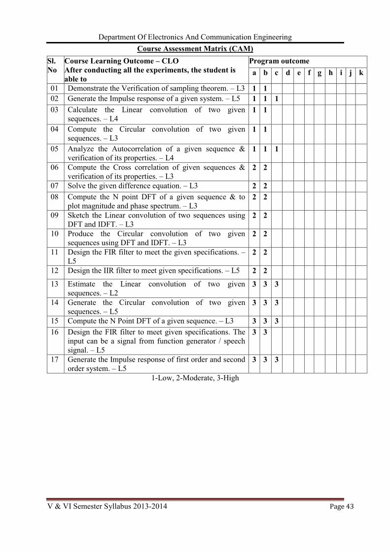
Department Of Electronics And Communication Engineering
V & VI Semester Syllabus 2013-2014 ���������������������������������������������������������������
��
Course Assessment Matrix (CAM)
1-Low, 2-Moderate, 3-High
Sl. No
Course Learning Outcome – CLO After conducting all the experiments, the student is able to
Program outcomea b c d e f g h i j k
01 Demonstrate the Verification of sampling theorem. – L3 1 1 02 Generate the Impulse response of a given system. – L5 1 1 1 03 Calculate the Linear convolution of two given
sequences. – L4 1 1
04 Compute the Circular convolution of two given sequences. – L3
1 1
05 Analyze the Autocorrelation of a given sequence & verification of its properties. – L4
1 1 1
06 Compute the Cross correlation of given sequences & verification of its properties. – L3
2 2
07 Solve the given difference equation. – L3 2 2 08 Compute the N point DFT of a given sequence & to
plot magnitude and phase spectrum. – L3 2 2
09 Sketch the Linear convolution of two sequences using DFT and IDFT. – L3
2 2
10 Produce the Circular convolution of two given sequences using DFT and IDFT. – L3
2 2
11 Design the FIR filter to meet the given specifications. – L5
2 2
12 Design the IIR filter to meet given specifications. – L5 2 2
13 Estimate the Linear convolution of two given sequences. – L2
3 3 3
14 Generate the Circular convolution of two given sequences. – L5
3 3 3
15 Compute the N Point DFT of a given sequence. – L3 3 3 3 16 Design the FIR filter to meet given specifications. The
input can be a signal from function generator / speech signal. – L5
3 3
17 Generate the Impulse response of first order and second order system. – L5
3 3 3

Department Of Electronics And Communication Engineering
V & VI Semester Syllabus 2013-2014 ���������������������������������������������������������������
��
�
Course Title : OPTICAL AND ANALOG COMMUNICATION LABORATORY Course Code: P13ECL58 Semester : V L-T-P-H:0 – 0 – 3-3 Credits:1.5 Contact Period : Lecture :39 Hrs., Exam: 3Hrs. Weightage :CIE:50% SEE:50%
Course Learning Objectives (CLOs)This course aims to 1. Experiment the attenuation and dispersion in optical fiber. 2. Measure the bending loss and numerical aperture in optical fiber. 3. Experiment the characteristics of LASER and photo diode. 4. Demonstrate the working analog and digital optical link. 5. Experiment the working of TDM of digital signals. 6. Demonstrate the working of an Erbium Doped Fiber Amplifier. 7. Demonstrate the working of WDM, MUX and DEMUX. 8. Provide the basic practical knowledge of modulation, demodulation, filtering, application
of 555 timers, fiber optic cable, characteristics of optical source and optical detector, TDM, MUX and DEMUX
9. Demonstrate the working of AM, PAM and its detection. 10. Demonstrate the working of PPM and FM. 11. Design the second order active LPF, HPF and BPF. 12. Design the Astable and Monostable multivibrators using 555 timer.
Course ContentA. EXPERIMENTS ON OPTICAL COMMUNICATION:01 Analog and Digital Fiber optic links 02 Bending loss and Numerical aperture measurement of optical fiber. 03 Attenuation and Dispersion in optical fiber. 04 LASER diode and photo diode characterization. 05 Time Division Multiplexing of digital signals. 06 Characterization of an Erbium Doped Fiber Amplifier. 07 Characterization of WDM MUX and DEMUX.
B. EXPERIMENTS ON ANALOG COMMUNICATION:08 Amplitude Modulation and Detection in time domain and its observation in frequency
domain (Use Spectrum Analyzer). 09 Pulse Amplitude Modulation and detection, using 555 timer. 10 Pulse Position Modulation using 555 timer. 11 Pulse Width Modulation using 555 timer. 12 Frequency Modulation using 8038/2206 in time domain and in frequency domain. 13 Second order active filters using op-Amp: LPF, HPF and BPF.
Course Learning Outcome After conducting all the experiments the student is able to 01 Experiment the attenuation and dispersion in optical fiber. – L4 02 Determine the bending loss and numerical aperture – L3 03 Experiment the characteristics of LASER and photo diode. – L4 04 Demonstrate the working analog and digital optic link. – L3 05 Experiment the working of TDM of digital signals. – L4 06 Demonstrate the working of an Erbium Doped Fiber Amplifier. – L3 07 Demonstrate the working WDM MUX and DMUX. – L3 08 Demonstrate the working of AM, PAM and its detection. – L3
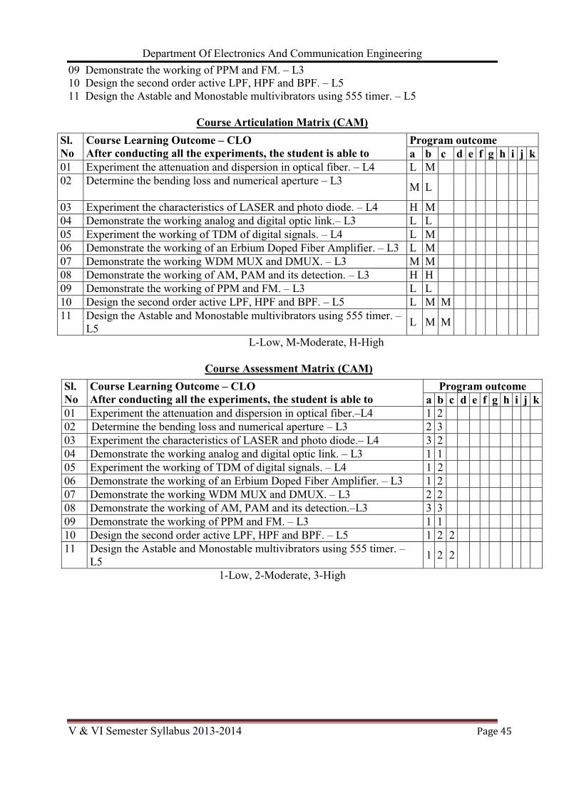
Department Of Electronics And Communication Engineering
V & VI Semester Syllabus 2013-2014 ����������������������������������������������������������������
��
09 Demonstrate the working of PPM and FM. – L3 10 Design the second order active LPF, HPF and BPF. – L5 11 Design the Astable and Monostable multivibrators using 555 timer. – L5
Course Articulation Matrix (CAM)
L-Low, M-Moderate, H-High
Course Assessment Matrix (CAM)
1-Low, 2-Moderate, 3-High
Sl. No
Course Learning Outcome – CLO After conducting all the experiments, the student is able to
Program outcome a b c d e f g h i j k
01 Experiment the attenuation and dispersion in optical fiber. – L4 L M 02 Determine the bending loss and numerical aperture – L3 M L
03 Experiment the characteristics of LASER and photo diode. – L4 H M 04 Demonstrate the working analog and digital optic link.– L3 L L 05 Experiment the working of TDM of digital signals. – L4 L M 06 Demonstrate the working of an Erbium Doped Fiber Amplifier. – L3 L M 07 Demonstrate the working WDM MUX and DMUX. – L3 M M 08 Demonstrate the working of AM, PAM and its detection. – L3 H H 09 Demonstrate the working of PPM and FM. – L3 L L 10 Design the second order active LPF, HPF and BPF. – L5 L M M 11 Design the Astable and Monostable multivibrators using 555 timer. –
L5 L M M
Sl. No
Course Learning Outcome – CLO After conducting all the experiments, the student is able to
Program outcome a b c d e f g h i j k
01 Experiment the attenuation and dispersion in optical fiber.–L4 1 2 02 Determine the bending loss and numerical aperture – L3 2 3 03 Experiment the characteristics of LASER and photo diode.– L4 3 2 04 Demonstrate the working analog and digital optic link. – L3 1 1 05 Experiment the working of TDM of digital signals. – L4 1 2 06 Demonstrate the working of an Erbium Doped Fiber Amplifier. – L3 1 2 07 Demonstrate the working WDM MUX and DMUX. – L3 2 2 08 Demonstrate the working of AM, PAM and its detection.–L3 3 3 09 Demonstrate the working of PPM and FM. – L3 1 1 10 Design the second order active LPF, HPF and BPF. – L5 1 2 2 11 Design the Astable and Monostable multivibrators using 555 timer. –
L5 1 2 2
Department Of Electronics And Communication Engineering
V & VI Semester Syllabus 2013-2014 ����������������������������������������������������������������
��
Course Title : ANALOG CMOS VLSI DESIGN Course Code: P13EC61 Semester : VI L-T-P-H: 4 – 0 – 0-4 Credits:4 Contact Period : Lecture :52 Hrs., Exam: 3Hrs. Weightage :CIE:50% SEE:50%
Course Learning Objectives (CLOs)This course aims to 1. Analyze the analog CMOS integrated circuits. 2. Describe the basic MOS device physics and more advanced properties and fabrication
details. 3. Describe the small signal and large signal analysis of amplifiers. 4. Explain the working of various single stage MOS amplifiers. 5. Describe the operation of differential amplifier and different types of Current mirrors and
their applications. 6. Provide the understanding of the concept of band gap references and discuss the speed
and noise issues. 7. Discuss the elementary switched capacitor circuit and effect of non–linearity and miss–
match. 8. Explain the condition for oscillation and design of different types of oscillators. 9. Design the Phase Locked Loops and its applications.
Course ContentUNIT – I
Basic MOS Device Physics: General Considerations, MOS I/V Characteristics, Second– Order Effects, MOS Device Models. Single– Stage Amplifiers: Basic Concepts, Common–Source Stage, Source Follower, Common–Gate Stage, Cascode Stage, Choice of Device Models. Text: 2.1 to 2.4 and 3.1 to 3.6 11 Hrs
UNIT – II Differential Amplifiers: Single– Ended and Differential Operation, Basic Differential Pair, Common–Mode Response, Differential Pair with MOS Loads, Gilbert Cell. Passive and Active Current Mirrors: Basic Current Mirrors, Cascode Current Mirrors, Active Current Mirrors, Text: 4.1 to 4.5 and 5.1 to 5.3 11 Hrs
UNIT – III Bandgap References: General Considerations, Supply–Independent Biasing, Temperature– Independent References, PTAT Current Generation, Constant–Gm Biasing, Speed and Noise Issues, Case Study. Introduction to Switched– Capacitor Circuits: General Considerations, Sampling Switches, Switched– Capacitor Amplifiers, Switched–Capacitor Integrator, Switched–Capacitor Common–Mode Feedback. Text: 11.1 to 11.7 and 12.1 to 12.5 10 Hrs
UNIT – IV Oscillators: General Considerations, Ring Oscillators, LC Oscillators, Voltage–Controlled Oscillators, Mathematical Model of VCOs. Text: 14.1 to 14.5 10 Hrs
UNIT – V Phase– Locked Loops: Simple PLL, Charge– Pump PLLs and Non–ideal Effects in PLLs, Delay–Locked Loops and Applications. Text: 15.1 to 15.5 10 Hrs TEXT BOOK:
Department Of Electronics And Communication Engineering
V & VI Semester Syllabus 2013-2014 �������������������������������������������������������������� �
��
“Design of Analog CMOS Integrated Circuits”, Behzad Razavi, Tata Mcgraw Hill, 2001. REFERENCE BOOKS: 1. “CMOS Analog Circuit Design”, Phillip E. Allen, Douglas R. Holberg, Oxford
University Press, 2003 2. “CMOS Circuit Design, Layout and Simulation”, R. Jacob Baker, Harry W. Li, David E.
Boyce, Prentice Hall of India, 2005 Course Outcome
After learning all the units of the course, the student is able to 01 Describe the physics of MOSFETs that is necessary for basic analog design & low
frequency behaviour of single stage amplifiers and analysis of different parameters using small signal and large signal analysis. – L1 (Unit – I)
02 Explain the importance of current sources in single stage and differential amplifiers and design of current mirrors, differential amplifier design and analysis and Gilbert cell operation. – L2 (Unit – II)
03 Explain the common class of discrete time system called switched capacitor circuits. – L2 (Unit – III)
04 Design the CMOS oscillators such as VCOs. – L5 (Unit – IV) 05 Design the PLLs using CMOS technology. – L5 (Unit – V) 06 Classify the different types of PLLs. – L2 (Unit – V)
Topic Learning Outcome (TLO)After learning all the topics of UNIT– I, the student is able to Explain the General Considerations of MOS devices. – L2 01 Discuss the MOS I/V Characteristics. – L2 02 Explain the Second–Order Effects in MOS devices. – L2 03 Describe the different MOS Device Models. – L1 04 Explain the Basic Concepts Common– Source Stage Source Follower. – L2 05 Design the Common–Gate Stage amplifier. – L3 06 Explain the operation of Cascode Stage amplifier. – L2 07 Discuss the Choice of Device Models. – L2
After learning all the topics of UNIT– II, the student is able to 01 Explain the basic operation of Single–Ended amplifier. – L2 02 Describe the operation of Differential amplifier. – L1 03 Explain the operation of Basic Differential Pair. – L2 04 Discuss the Common–Mode Response of Differential amplifier. – L2 05 Design the Differential Pair amplifier with MOS Loads. – L3 06 Explain the operation of Gilbert Cell. – L2 07 Discuss the various Basic Current Mirrors. – L2 08 Explain the operation of Cascode Current Mirrors. – L2 09 Solve the problems on Current Mirrors. – L3 10 Explain the operation of active Current Mirrors. – L2
After learning all the topics of UNIT– III, the student is able to 01 List the General Considerations in bandgap reference. – L1 02 Explain the Supply–Independent Biasing of MOS Circuit. – L2 03 Describe the Temperature–Independent References of MOS circuit. – L1 04 Explain the PTAT Current Generation in MOS circuit. – L2 05 Discuss the Constant–Gm Biasing. – L2 06 Discuss the Speed and Noise Issues in MOS devices– L2 07 List the General Considerations in Switched–Capacitor of MOS devices. – L1
Department Of Electronics And Communication Engineering
V & VI Semester Syllabus 2013-2014 ����������������������������������������������������������������
��
08 Explain the concept of Sampling Switches in MOS. – L2 09 Explain the circuit of Switched–Capacitor Integrator. – L2 10 Discuss the effect of Switched–Capacitor in MOS circuits. – L2 11 Explain the concept Common–Mode Feedback. – L2
After learning all the topics of UNIT– IV, the student is able to 01 Explain the General Considerations for oscillators. – L2 02 Explain the operation of Ring Oscillators. – L2 03 Discuss the different LC Oscillators operation. – L2 04 Explain the operation of Voltage– Controlled Oscillators. – L2 05 Express the Mathematical Model of VCOs. – L2
After learning all the topics of UNIT– V, the student is able to 01 Explain the Simple PLL operation. – L2 02 Discuss the different Charge– Pump PLLs operation. – L2 03 Explain the Non–ideal Effects in PLLs. – L2 04 Explain the working of Delay–Locked Loops. – L2 05 Discuss the Applications of PLLs. – L2
Review Questions1. Explain VI characteristics of MOSFET. 2. Derive equation for drain current and transconductance at different region of operations. 3. Explain with diagram how MOSFET can be used as current source. 4. Differentiate between nmos and pmos and write spice model of nmos transistor. 5. Explain CS stage amplifier with resistive load and derive an equation for voltage gain. 6. Explain CS stage amplifier with diode connected load and derive an equation for voltage
gain. 7. Derive an equation for voltage gain in source degeneration of CS amplifier. 8. In the circuit of figure M1 is biased in saturation with a drain current equal to I1.The
current source Is=0.75I1 is added to circuit. Find gain of circuit.
9. Explain CS stage with current source load. 10. Derive an equation for gain of CS stage with source degeneration. 11. Derive an equation for gain of Source follower amplifier. 12. Explain Basic Cascode stage amplifiers. 13. Explain Folded Cascode amplifier. 14. Explain why differential amplifiers are preferred over single ended amplifiers. 15. Explain basic differential pair amplifier. 16. Explain qualitative analysis of differential amplifier. 17. Explain quantitative analysis of differential amplifier. 18. Derive Common mode voltage gain of differential amplifier.
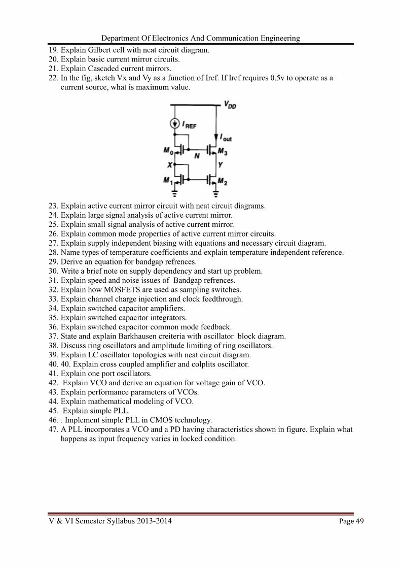
Department Of Electronics And Communication Engineering
V & VI Semester Syllabus 2013-2014 ����������������������������������������������������������������
��
19. Explain Gilbert cell with neat circuit diagram. 20. Explain basic current mirror circuits. 21. Explain Cascaded current mirrors. 22. In the fig, sketch Vx and Vy as a function of Iref. If Iref requires 0.5v to operate as a
current source, what is maximum value.
23. Explain active current mirror circuit with neat circuit diagrams. 24. Explain large signal analysis of active current mirror. 25. Explain small signal analysis of active current mirror. 26. Explain common mode properties of active current mirror circuits. 27. Explain supply independent biasing with equations and necessary circuit diagram. 28. Name types of temperature coefficients and explain temperature independent reference. 29. Derive an equation for bandgap refrences. 30. Write a brief note on supply dependency and start up problem. 31. Explain speed and noise issues of Bandgap refrences. 32. Explain how MOSFETS are used as sampling switches. 33. Explain channel charge injection and clock feedthrough. 34. Explain switched capacitor amplifiers. 35. Explain switched capacitor integrators. 36. Explain switched capacitor common mode feedback. 37. State and explain Barkhausen creiteria with oscillator block diagram. 38. Discuss ring oscillators and amplitude limiting of ring oscillators. 39. Explain LC oscillator topologies with neat circuit diagram. 40. 40. Explain cross coupled amplifier and colplits oscillator. 41. Explain one port oscillators. 42. Explain VCO and derive an equation for voltage gain of VCO. 43. Explain performance parameters of VCOs. 44. Explain mathematical modeling of VCO. 45. Explain simple PLL. 46. . Implement simple PLL in CMOS technology. 47. A PLL incorporates a VCO and a PD having characteristics shown in figure. Explain what
happens as input frequency varies in locked condition.
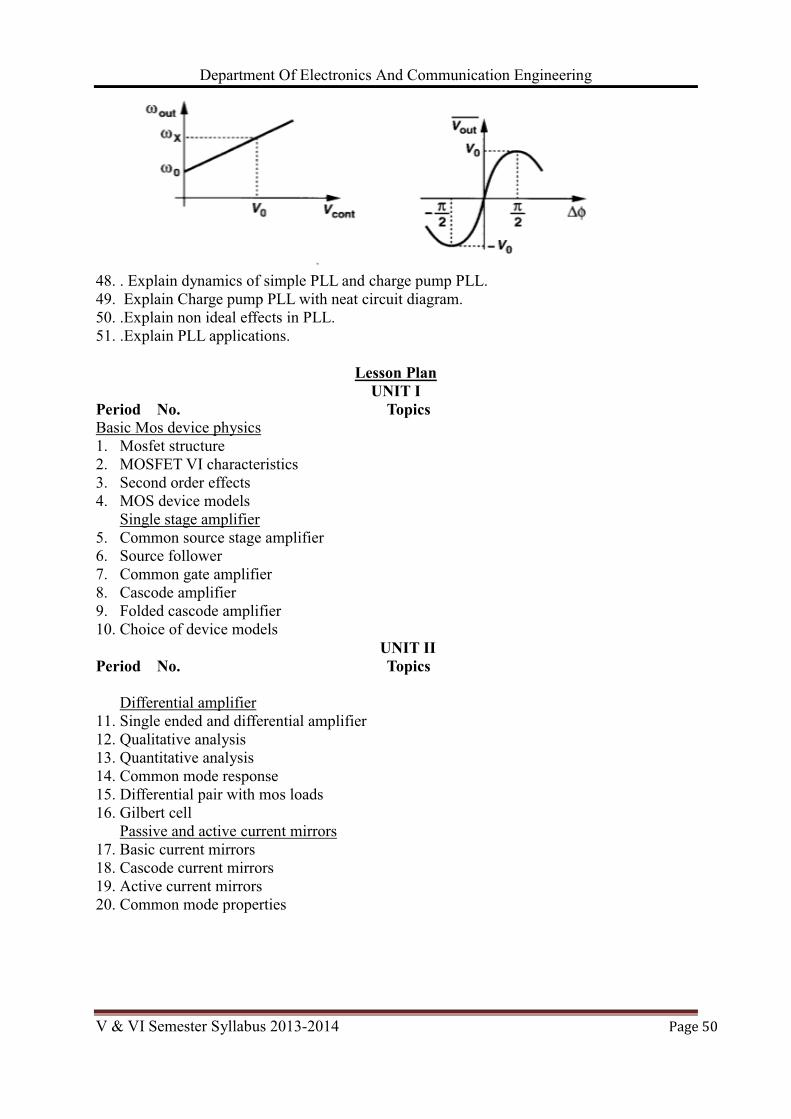
Department Of Electronics And Communication Engineering
V & VI Semester Syllabus 2013-2014 �����������������������������������������������������������������
��
48. . Explain dynamics of simple PLL and charge pump PLL. 49. Explain Charge pump PLL with neat circuit diagram.50. .Explain non ideal effects in PLL. 51. .Explain PLL applications.
Lesson PlanUNIT I
Period No. Topics Basic Mos device physics1. Mosfet structure 2. MOSFET VI characteristics 3. Second order effects 4. MOS device models
Single stage amplifier5. Common source stage amplifier 6. Source follower 7. Common gate amplifier 8. Cascode amplifier 9. Folded cascode amplifier 10. Choice of device models
UNIT II Period No. Topics
Differential amplifier11. Single ended and differential amplifier 12. Qualitative analysis 13. Quantitative analysis 14. Common mode response 15. Differential pair with mos loads 16. Gilbert cell
Passive and active current mirrors17. Basic current mirrors 18. Cascode current mirrors 19. Active current mirrors 20. Common mode properties

Department Of Electronics And Communication Engineering
V & VI Semester Syllabus 2013-2014 �����������������������������������������������������������������
��
UNIT III Period No. Topics
Bandgap refrences21. Supply independent biasing 22. Temperature independent biasing 23. Constant gm biasing 24. Speed and noise issues Introduction to switched capacitors25. General considerations 26. Sampling switches 27. Switched capacitor amplifiers 28. Switched capacitor integrator 29. Switched capacitor common mode feedback
UNIT IV Period No. Topics 30. Oscillators General considerations 31. Ring oscillators 32. LC oscillators 33. Colplitts oscillator 34. Voltage controlled oscillators 35. Mathematical modelling of VCO.
UNIT V Period No. Topics
PLL36. Simple PLL 37. Charge pump PLL. 38. Non ideal effects in PLL. 39. Delay locked loops

Department Of Electronics And Communication Engineering
V & VI Semester Syllabus 2013-2014 �����������������������������������������������������������������
��
Course Articulation Matrix (CAM)Sl. NoCourse Learning Outcome – CLO
After learning all the units of the course, the student is able to
Programme outcome
a b c d e f g h i j k01 Describe the physics of MOSFETs that is necessary
for basic analog design & low frequency behaviourof single stage amplifiers and analysis of differentparameters using small signal and large signalanalysis. – L1 (Unit – I)
L1L M
02 Explain the importance of current sources in singlestage and differential amplifiers and design of currentmirrors, differential amplifier design and analysisand Gilbert cell operation. – L2 (Unit – II)
L2L M H
03 Explain the common class of discrete time systemcalled switched capacitor circuits. – L2 (Unit – III) L2 L M H
04 Design the CMOS oscillators such as VCOs. – L5(Unit – IV) L5 L M H
05 Design the PLLs using CMOS technology. – L5(Unit – V) L5 L M H
06 Classify the different types of PLLs. – L2 (Unit – V)L2 L M
L-Low, M-Moderate, H-High
Course Assessment Matrix (CAM)Sl. No Course Learning Outcome – CLO
After learning all the units of the course, the student is able to
Programme outcome
a b c d e f g h i j k01 Describe the physics of MOSFETs that is necessary
for basic analog design & low frequency behaviour of single stage amplifiers and analysis of different parameters using small signal and large signal analysis. – L1 (Unit – I)
L11 2
02 Explain the importance of current sources in single stage and differential amplifiers and design of current mirrors, differential amplifier design and analysis and Gilbert cell operation. – L2 (Unit – II)
L2 1 2 3
03 Explain the common class of discrete time system called switched capacitor circuits. – L2 (Unit – III) L2 1 2 3
04 Design the CMOS oscillators such as VCOs. – L5 (Unit – IV) L5 1 2 3
05 Design the PLLs using CMOS technology. – L5 (Unit – V) L5 1 2 3
06 Classify the different types of PLLs. – L2 (Unit – V)L2 1 2
1-Low, 2-Moderate, 3-High
Department Of Electronics And Communication Engineering
V & VI Semester Syllabus 2013-2014 ����������������������������������������������������������������
��
Course Title : COMPUTER COMMUNICATION NETWORKS Course Code: P13EC62 Semester : VI L-T-P-H: 4 – 0 – 0-4 Credits:4 Contact Period : Lecture :52 Hrs., Exam: 3Hrs. Weightage :CIE:50% SEE:50%
Prerequisite course for: 1. GSM Communication and Networks – P13EC74
Course Learning Objectives (CLOs)This course aims to 1. Provide the understanding of layering in computer networks. 2. Provide the understanding of different protocol stacks (TCP/IP); understand functions and
protocols within a layer. 3. Provide the understanding of how the layers fit together and finally understand how the
Internet works. 4. Discuss the different application architectures and Processes communicating. 5. Provide the understanding of the basic principles behind transport layer services and
protocols (UDP, TCP). 6. Provide the understanding of network layer's host–to–host communication service. 7. Discussing between the forwarding and routing functions of the network layer. 8. Provide the understanding of link layer services, the principles underlying its operation,
and a number of important specific protocols that use these principles in implementing link layer services.
Course ContentUNIT – I
Computer Networks and the Internet: What Is the Internet?, The Network Edge, The Network Core, Delay, Loss, and throughput in Packet–Switched Networks, Protocol Layers and their Service Models, History of computer networking and Internet. Text: 1.1 to 1.7 10 Hrs
UNIT – II Application Layer: Principles of Network Applications, The Web and HTTP, File Transfer: FTP, Electronic Mail in the Internet, DNS–The Internet’s Directory Service, P2P File Applications. Text: Chapter 2.1 to 2.6 10 Hrs
UNIT – III Transport Layer: Introduction and Transport– Layer Services, Multiplexing and De–multiplexing. Connectionless Transport: UDP, Principles of Reliable Data Transfer, Connection–Oriented Transport: TCP. Text: 3.1 to 3.5 11 Hrs
UNIT – IV The Network Layer: Introduction, Virtual Circuit and Datagram Networks, What’s Inside a Router? The Internet Protocol (IP): Forwarding and Addressing in the Internet, Routing Algorithms, Broadcast and Multicast Routing Text: 4.1 to 4.5 And 4.7 10 Hrs
UNIT – V The Link Layer and Local Area Networks: Link Layer: Introduction and Services, Error–Detection and Correction Techniques Multiple Access Protocols Link–Layer Addressing, Ethernet Interconnections: Hubs and Switches

Department Of Electronics And Communication Engineering
V & VI Semester Syllabus 2013-2014 ����������������������������������������������������������������
��
PPP: The Point–to–Point Protocol Link Virtualization: A Network as a Link Layer Text: 5.1 to 5.8 11 Hrs
TEXT BOOK: “Computer Networks”, James F. Kurose and Keith W. Ross Pearson education, 5th Edition, 2013
REFERENCE BOOKS: 1. “Data Communication and Networking”, Behrouz Forouzan, TMH, 4th Edition 2. “Computer Networks”, A Top down Approach by Behrouz Forouzan, Firouz Mosharraf,
McGraw–Hill. 3. “Data and Computer Communication”, William Stallings, PHI, 6th Edition
Course OutcomesAfter learning all the units of the course, the student is able to 01 Explain the concept of internet infrastructure and services offered. – L1 (Unit – I) 02 Calculate the Delay & loss in packet– switched networks. – L4 (Unit – I) 03 Describe the Web, HTTP, FTP, Electronic Mail, SMTP, POP3, IMAP and DNS. – L1
(Unit – II) 04 Explain TCP and UDP transport layer protocol principles. – L3 (Unit – III) 05 Discuss the VCN,DGN’s and network layer protocols with IPV4 and IPV6 formats.-
L3(Unit-IV) 06 Discuss network layer services, Access protocols, Ethernet hubs, switches and PPP
virtualization.-L2(Unit-V)
Topic Learning OutcomesAfter learning all the topics of UNIT– I, the student is able to 01 Define the Internet and Explain Network edge and Network core. – L1 02 Describe the Internet's connection–oriented service provides reliable transport. – L1 03 Describe the Network access, physical media and ISPs. – L1 04 Calculate the Delay & loss in packet–switched networks. – L4 05 Draw the five layers in the Internet protocol stack. – L4 06 State the principle responsibilities for each of the five layers in the Internet protocol stack.
– L1
After learning all the topics of UNIT– II, the student is able to 01 List the various network–application user agents that you use on a daily basis. – L1 02 Explain the application architectures and Processes communicating. – L2 03 Describe the Web, HTTP, FTP, Electronic Mail, SMTP, POP3, IMAP and DNS. – L1 04 Discuss the P2P file sharing. – L2
After learning all the topics of UNIT– III, the student is able to 01 Explain the transport layer protocol provides for logical communication between
application processes running on different hosts. – L2 02 Discuss the Transport–layer services. – L2 03 Explain the Multiplexing and de–multiplexing. – L2 04 Write the UDP segment structure and explain its components. – L3 05 Describe the principles of reliable data transfer with service model and service
implementation. – L2 06 Write the TCP segment structure and explain its components. – L3
Department Of Electronics And Communication Engineering
V & VI Semester Syllabus 2013-2014 �����������������������������������������������������������������
��
After learning all the topics of UNIT– IV, the student is able to 01 Describe the principles behind network layer services. – L1 02 Compare the Virtual circuit and datagram networks. – L4 03 Explain the components of IPv4 and IPv6 datagram format. – L3 04 Explain the ICMP protocol. – L2 05 Compare the link state and distance–vector algorithms. – L4 06 Explain the broadcast and multicast routing algorithms. – L2 After learning all the topics of UNIT– V, the student is able to 01 List the possible services of link layer. – L1 02 Discuss the error detection and correction techniques in link layer. – L2 03 Explain the random access protocols (ALOHA, SLOTTED ALOHA, CSMA,
CSMA/CD). – L2 04 Explain the taking–turn and ARP protocols. – L2 05 Define the MAC address. – L1 06 Differentiate the switches versus routers. – L4 07 Describe the MPLS and PPP with data format. – L1
Review Questions1 Define the Internet and Explain Network edge and Network core. 2 Describe the Internet's connection–oriented service provides reliable transport. 3 Describe the Network access, physical media and ISPs. 4 Calculate the Delay & loss in packet–switched networks. 5 Explain queuing delay and its dependency on traffic intensity. 6 Compare Circuit switched network with packet switched network. 7 Draw the five layers in the Internet protocol stack. 8 State the principle responsibilities for each of the five layers in the Internet protocol stack. 9 List the various network–application user agents that you use on a daily basis. 10 Explain the application architectures and Processes communicating. 11 Describe the Web, HTTP, FTP, Electronic Mail, SMTP, POP3, IMAP and DNS. 12 What are cookies? 13 Describe message/commands format of HTTP, FTP and SMTP. 14 Compare HTTP and FTP. 15 What is MIME where and why it is used? 16 Discuss the P2P file sharing. 17 Explain the transport layer protocol provides for logical communication between
application processes running on different hosts. 18 Discuss the Transport–layer services. 19 Explain the Multiplexing and de–multiplexing. 20 Why most internet application prefers UDP? 21 Write the UDP segment structure and explain its components. 22 Describe the principles of reliable data transfer with service model and service
implementation. 23 With requires FSM/diagrams explain Goback-N protocol 24 Write the TCP segment structure and explain its components. 25 Discuss the Round-Trip Time estimation and Timeout.26 Explain congestion control. 27 Describe the principles behind network layer services. 28 Compare the Virtual circuit and datagram networks. 29 Difference between routing and forwarding.
Department Of Electronics And Communication Engineering
V & VI Semester Syllabus 2013-2014 �����������������������������������������������������������������
��
30 Describe packet loss at input and output ports. 31 Explain IGMP protocol. 32 Describe network address translation. 33 Explain the components of IPv4 and IPv6 datagram format. 34 Calculate binary equivalent of the given IP address. 35 Explain the ICMP protocol. 36 Compare the link state and distance–vector algorithms. 37 Explain Hierarchical Routing. 38 Explain the broadcast and multicast routing algorithms. 39 List the possible services of link layer. 40 Discuss the error detection and correction techniques in link layer. 41 Explain the random access protocols (ALOHA, SLOTTED ALOHA, CSMA,
CSMA/CD). 42 Compare CSMA and CSMA/CD. 43 Describe Taking-Turns Protocol. 44 Explain in brief DHCP. 45 Explain the taking–turn and ARP protocols. 46 Define the MAC address. 47 With an illustration explain switch forwarding and filtering. 48 Differentiate the switches versus routers. 49 List out the IETF requirements of PPP. 50 Describe the MPLS and PPP with data format.
Lesson PlanUNIT-I
Period No. Topics 1. Internet, Network Edge 2. Network Core 3. Network Core 4. Delay, Loss in Packet Switched Networks 5. Delay, Loss in Packet Switched Networks 6. Delay, Loss in Packet Switched Networks 7. Protocol Layers and Service Models 8. Protocol Layers and Service Models 9. Protocol Layers and Service Models 10. History of computer networking and Internet
UNIT-II Period No. Topics
1. Principles of Network Applications2. Principles of Network Applications3. The Web and HTTP 4. HTTP Messages 5. HTTP Messages 6. File Transfer: FTP 7. Electronic Mail in the Internet 8. DNS–The Internet’s Directory Service 9. P2P File Applications 10. P2P File Applications

Department Of Electronics And Communication Engineering
V & VI Semester Syllabus 2013-2014 ��������������������������������������������������������������� �
��
UNIT-III Period No. Topics
1. Transport Layer: Introduction 2. Transport– Layer Services 3. Transport– Layer Services 4. Multiplexing and De–multiplexing 5. Multiplexing and De–multiplexing. 6. Connectionless Transport: UDP 7. Connectionless Transport: UDP 8. Principles of Reliable Data Transfer 9. Principles of Reliable Data Transfer 10. Connection–Oriented Transport: TCP 11. Connection–Oriented Transport: TCP
UNIT-IV Period No. Topics
1. The Network Layer: Introduction 2. Virtual Circuit and Datagram Networks 3. Virtual Circuit and Datagram Networks 4. What’s Inside a Router? 5. The Internet Protocol (IP): Forwarding and Addressing in the Internet 6. Routing Algorithms 7. Routing Algorithms 8. Routing Algorithms 9. Broadcast and Multicast Routing 10. Broadcast and Multicast Routing
UNIT-V Period No. Topics
1. The Link Layer and Local Area Networks: Link Layer: Introduction 2. The Link Layer and Local Area Networks: Link Layer: Introduction 3. Link Layer: Services 4. Link Layer: Services 5. Error–Detection and Correction Techniques 6. Multiple Access Protocols 7. Multiple Access Protocols 8. Link–Layer Addressing 9. Ethernet Interconnections: Hubs and Switches 10. PPP: The Point–to–Point Protocol Link Virtualization 11. PPP: The Point–to–Point Protocol Link Virtualization: A Network as a Link Layer

Department Of Electronics And Communication Engineering
V & VI Semester Syllabus 2013-2014 �����������������������������������������������������������������
��
Course Articulation Matrix (CAM)
L-Low, M-Moderate, H-High
Course Assessment Matrix (CAM)
1-Low, 2-Moderate, 3-High
Sl. No
Course Learning Outcome – CLO After learning all the units of the course, the student is able to
Program Outcome (ABET/NBA-(3a-k))
a b c d e f g h i j k01 Explain the concept of internet infrastructure and
services offered. (Unit – I) L1 L L
02 Calculate the Delay & loss in packet– switched networks. (Unit – I)
L4 L L
03 Describe the Web, HTTP, FTP, Electronic Mail, SMTP, POP3, IMAP and DNS. (Unit – II)
L1 L L L
04 Explain TCP and UDP transport layer protocol principles. (Unit – III)
L3 L L L
05 Discuss the VCN,DGN’s and network layer protocols with IPV4 and IPV6 formats.(Unit-IV)
L3 L L
06 Discuss network layer services, Access protocols, Ethernet hubs, switched and PPP virtualization.(Unit-V)
L2 L L L
Sl. No
Course Learning Outcome – CLO After learning all the units of the course, the student is able to
Program Outcome (ABET/NBA-(3a-k))
a b c d e f g h i j k01 Explain the concept of internet infrastructure and
services offered. (Unit – I) L1 1 1
02 Calculate the Delay & loss in packet– switched networks. (Unit – I)
L4 1 1
03 Describe the Web, HTTP, FTP, Electronic Mail, SMTP, POP3, IMAP and DNS. (Unit – II)
L1 1 1 1
04 Explain TCP and UDP transport layer protocol principles. (Unit – III)
L3 1 1 1
05 Discuss the VCN,DGN’s and network layer protocols with IPV4 and IPV6 formats.(Unit-IV)
L3 1 1
06 Discuss network layer services, Access protocols, Ethernet hubs, switched and PPP virtualization.(Unit-V)
L2 1 1 1

Department Of Electronics And Communication Engineering
V & VI Semester Syllabus 2013-2014 �����������������������������������������������������������������
��
Course Title : MICROWAVE DEVICES AND INTEGRATED CIRCUITS Course Code: P13EC63 Semester : VI L-T-P-H: 4 – 0 – 0-4 Credits: 4 Contact Period : Lecture :52 Hrs., Exam: 3Hrs. Weightage :CIE:50% SEE:50%
Course Learning Objectives (CLOs)This course aims to 1. Provide the basic knowledge of Microwave transmission lines. 2. Discuss the importance of Microwave Waveguides and components. 3. Provide the understanding of working principles of Microwave linear beam tubes like
Klystrons, Helix TWT. 4. Describe the Microwave Network theories and Passive Devices. 5. Provide the understanding of concepts of Transfer Electron Devices, Avalanche transit
time Devices and Parametric Amplifiers. 6. Explain the various planar Transmission Lines and Design of Microwave Integrated
circuits. 7. Solve the numerical Problems on Smith chart, Impedance matching, Microwave Network
Theory.
Course Content
UNIT – I Microwave transmission lines: Introduction, transmission lines equations and solutions, reflection and transmission coefficients, standing waves and SWR, line impedance and line admittance. Smith chart, impedance matching using single stubs. Text 1: 3.0 – 3.6.1 10 Hrs
UNIT – II Microwave waveguides and components: Introduction, TE, TM and TEM waves in rectangular and circular wave guide, microwave cavities, directional couplers, circulators and isolators. Microwave Linear beam Tubes (O Type): Klystron, Multi cavity Klystron Amplifier, reflex Klystron, Helix – TWT. Text 1: 4.0, 4.1.2, 4.1.3, 4.2.2, 4.2.3, 4.2.4, 4.3, 4.5, 4.6 and 9.2 to 9.5 11 Hrs
UNIT – III Microwave network theory and passive devices: Symmetrical Z and Y parameters, for reciprocal Networks, S matrix representation of multi port – networks, coaxial connectors and adapters, Phase shifters, Attenuators, Power dividers, Waveguide Tees, Magic tees. Text 2: 6.1, 6.2, 6.3, 6.4.1, 6.4.2, 6.4.14, 6.4.15, 6.4.16 11 Hrs
UNIT – IV Microwave diodes, Transfer electron devices: Introduction, GUNN Effect diodes – GaAs diode, RWH theory, Modes of operation, Avalanche transit time devices: READ diode, IMPATT diode, TRAPATT diode, BARITT diode, Parametric amplifiers Other diodes: PIN diodes, Tunnel diode, Varactor diode, Schottky barrier diodes. Text 1: 7.0 to 7.3, 8.1 to 8.4 Text 2: 10.5 to 10.7 10 Hrs
UNIT – V Planar Transmission Lines (Strip lines): Introduction, Micro strip lines, Parallel strip lines, Coplanar strip lines, Shielded strip Lines. Microwave integrated circuit Design: Introduction, types of MIC’s and their technology, hybrid technology, Monolithic Technology, MIC lumped and distributed elements. Text 1: 11.0, 11.1, 11.2, 11.3, 11.4 Text 2: 4.1, 4.2, 4.3, 4.4, 4.5 10 Hrs

Department Of Electronics And Communication Engineering
V & VI Semester Syllabus 2013-2014 �����������������������������������������������������������������
��
TEXT BOOK: 1. “Microwave Devices and Circuits”, Samuel Y Liao, 3rd Edition, Pearson Education. 2. “Microwave Engineering”, Annapurna Das, Sisir K Das, 2nd Edition, TMH.
REFERENCE BOOKS: 1. “Microwave Engineering”, David M Pozar, John Wiley, 2nd Edition, 2004 2. “Foundations For Microwave Engineering”, Robert E Collin, John Wiley & Sons Inc
(Sea) Pte Ltd, 2009. Course Outcome
After learning all the units of the course, the student is able to 01 Explain the microwave Transmission line equations and solutions. – L2 (Unit – I) 02 Discuss the TE, TM, TEM modes in circular and rectangular waveguides. – L2 (Unit – II) 03 Discuss the symmetrical Z and Y parameters for reciprocal networks. – L2 (Unit – III) 04 Explain the working of various microwave diodes. – L2 (Unit – IV) 05 Develop the expressions for characteristic impedance and losses in microstrip lines,
parallel striplines, coplanar and shielded striplines. – L5 (Unit – V) 06 Describe the fabrication process of MMIC and hybrid MIC. – L2 (Unit – V)
Topic Learning Outcome After learning all the topics of UNIT– I, the student is able to 1. Explain the microwave transmission line equations and solutions. – L2 2. Develop the expressions for reflection and transmission coefficients and Standing Wave
Ratio. – L5 3. Explain the line impedance, line admittance and smith chart. – L2 4. Solve the numerical problems on impedance matching and smith chart. – L3
After learning all the topics of UNIT– II, the student is able to 1. Discuss the TE, TM, TEM modes in rectangular and circular waveguides. – L2 2. Analyze the circulators, directional couplers and isolators. – L4 3. Develop the S matrix for directional coupler, circulators and isolators. – L5 4. Explain the concepts of klystron and helix–TWT. – L2
After learning all the topics of UNIT– III, the student is able to 1. Discuss the symmetrical Z and Y parameters for reciprocal networks. – L2 2. Analyze the multiport network using S–matrix. – L4 3. Solve the numerical problems on network theory. – L3 4. Describe the various microwave passive devices. – L2
After learning all the topics of UNIT– IV, the student is able to 1. Describe the working of Gunn diodes and modes of operation. – L2 2. Explain the working of avalanche transit time devices such as READ, IMPATT,
TRAPATT, BARITT diodes. – L2 3. Discuss the concepts of parametric amplifiers. – L24. Summarize the working of PIN, Tunnel, Varactor and Schottky barrier diodes. – L2
After learning all the topics of UNIT– V, the student is able to 1. Develop the expression for characteristic impedance and losses in microstrip lines,
parallel striplines, coplanar striplines and shielded striplines. – L5 2. Distinguish between the thick film and thin film technology. – L4 3. Describe the fabrication process of MMIC and hybrid MICs. – L2
Department Of Electronics And Communication Engineering
V & VI Semester Syllabus 2013-2014 �����������������������������������������������������������������
��
4. Explain why the lumped elements R, L and C cannot be used at high RF and microwave frequencies. – L2
Review Questions01 Develop the expressions for Reflection and Transmission coefficients and standing wave
Ratio. 02 Solve the numerical problems on smith chart and impedance matching. 03 Explain the concepts of directional couplers, circulators and isolators. 04 Analyze the microwave passive devices using S– matrix. 05 Solve the numerical problems on network theory. 06 Explain the working of various microwave diodes. 07 Distinguish between the thick film and thin film technology. 08 Drive the equation for line impedance. 09 Explain two-valley model theory. 10 Explain high field domain and its properties. 11 Briefly describe a micro strip line. 12 What is an S-matrix? State and prove symmetric property and unitary property of an ’S’
matrix. 13 Compare ABCD parameter with Z and Y parameter. 14 What are standing waves? Drive the relation between SWR and reflection coefficient of
transmission lines. 15 Derive the equation for the following at microwave frequency. i) Propagation constant ii)
Attenuation constant iii) Phase constant iv) Characteristic impedance & v) Phase velocity 16 Give the comparison between waveguide and co-axial cable. 17 How to realize the four –port circulator with directional couplers and 08 phase shifter?
Explain 18 Explain mechanism of oscillation in Reflex klystron oscillator with neat sketches? 19 Explain TWT amplifier with neat sketches? 20 Explain the relation between incident and reflected waves in terms of scattering
parameters for a two port network. Also explain physical significance of s- parameters. 21 Which properties are common in S,Z and Y matrices? 22 Two transmission lines of characteristic impedances Z1 and Z2 are joined at plane PP’
Express s- parameters in terms of impedances. 23 Explain with a neat sketch a precision rotary phase shifter. 24 Explain with relevant figures the fundamental concept of RWH theory. 25 Explain the principle of operation of read diode with suitable diagrams. 26 Draw the equivalent circuit for parametric amplifier and explain. 27 Obtain attenuation losses in parallel strip lines for both conductor and dielectric. 28 Distinguish between thick film and thin film technology. Describe the 10 fabrication
process of MMIC and hybrid MIC’s. 29 Describe the basic fabrication process of MOSFET’s?30 Compare the performance characteristics of TWTA and a klystron amplifier. 31 Express the relationship between incident and reflected waves in terms ‘S’-parameters,
‘Sij’ and describe the physical significance of S-parameters for two port reciprocal structures.
32 State and prove unitary property for a lossless junction in S-parameters. 33 With neat sketch explain precision type variable attenuator. 34 List out different types of co-axial connectors and their impedance. 35 With neat diagram explain the construction and operation of TRAPATT diode.
Department Of Electronics And Communication Engineering
V & VI Semester Syllabus 2013-2014 �����������������������������������������������������������������
��
36 State the three criterias of RWH theory. For band structures of semiconductor to exhibit negative resistance.
37 Write the advantages and disadvantages of Microstrip lines. 38 Drive the characteristics impedance of for Microstrip lines. 39 What are the two basic methods are adopted for manufacturing of ‘thick-film’ MIC’s and
explain its fabrication steps. 40 Explain with sketchs plate-through technique and Etch back technique. 41 Why conventional open –wire lines are not suitable for microwave transmission. 42 Drive the set of field equations for TEmn modes in rectangular wave guide. 43 Drive the expression for power flow through a co-axial line starting from field equations. 44 Describe the operating principles of the microwave tube that can be used as a low power
microwave oscillator. With neat illustration. 45 With a neat diagram, explain the working of precision type variable attenuator, write its s-
matrix and get the expression for attenuation in dB. 46 Explain the ports of Hybrid magic-T and obtain the S matrix of the magic-T. 47 What is “Transferred Electron effect”? Explain how this is used in a solid state device in
generating microwave oscillations. 48 What are the advantages and limitations of parametric amplifier. 49 Describe the hybrid IC techniques. 50 Obtain attenuation losses in parallel strip lines for both conductor and dielectric.
Lesson PlanUNIT – I
Period No. Topics 1. Microwave transmission lines: Introduction. 2. Transmission lines equations and solutions. 3. Reflection and transmission coefficients.4. Reflection and transmission coefficients. 5. Standing waves and SWR.6. Line impedance and line admittance. 7. Smith chart. 8. Smith chart. 9. Impedance matching using single stubs.10. Impedance matching using single stubs.
UNIT – II
Period No. Topics 11. Microwave waveguides and components: 12. Introduction. 13. TE, TM and TEM waves in rectangular and circular wave guide.14. TE, TM and TEM waves in rectangular and circular wave guide.15. Microwave cavities. 16. Directional couplers. 17. Circulators and isolators. 18. Microwave Linear beam Tubes (O Type): Klystron.19. Multi cavity Klystron Amplifier. 20. Reflex Klystron. 21. Helix – TWT.
Department Of Electronics And Communication Engineering
V & VI Semester Syllabus 2013-2014 ����������������������������������������������������������������
��
UNIT – III Period No. Topics 22. Microwave network theory and passive devices: 23. Symmetrical Z and Y parameters, for reciprocal Networks. 24. Symmetrical Z and Y parameters, for reciprocal Networks.25. S matrix representation of multi port – networks.26. S matrix representation of multi port – networks.27. Coaxial connectors and adapters. 28. Phase shifters. 29. Attenuators.30. Power dividers.31. Waveguide Tees. 32. Magic tees.
UNIT – IV Period No. Topics 33. Microwave diodes, Transfer electron devices: Introduction. 34. GUNN Effect diodes – GaAs diode. 35. RWH theory, Modes of operation. 36. Avalanche transit time devices: READ diode. 37. IMPATT diode, TRAPATT diode. 38. BARITT diode. 39. Parametric amplifiers Other diodes: PIN diodes. 40. Tunnel diode. 41. Varactor diode. 42. Schottky barrier diodes.
UNIT – V Period No. Topics 43. Planar Transmission Lines (Strip lines): Introduction 44. Micro strip lines. 45. Parallel strip lines. 46. Coplanar strip lines. 47. Shielded strip Lines. 48. Microwave integrated circuit Design: Introduction. 49. Types of MIC’s and their technology. 50. Hybrid technology. 51. Monolithic Technology. 52. MIC lumped and distributed elements.

Department Of Electronics And Communication Engineering
V & VI Semester Syllabus 2013-2014 ����������������������������������������������������������������
��
Course Articulation Matrix (CAM)
L-Low, M-Moderate, H-High
Course Assessment Matrix (CAM)
1-Low, 2-Moderate, 3-High
Sl. No
Course Learning Outcome – CLO After learning all the units of the course, the student is able to
Programme outcome
a b c d e f g h i j k01 Explain the microwave Transmission line
equations and solutions. – L2 (Unit – I) H M L
02 Discuss the TE, TM, TEM modes in circular and rectangular waveguides. – L2 (Unit – II) H L L
03 Discuss the symmetrical Z and Y parameters for reciprocal networks. – L2 (Unit – III) H M L
04 Explain the working of various microwave diodes. – L2 (Unit – IV) H L
05 Develop the expressions for characteristic impedance and losses in microstrip lines, parallel striplines, coplanar and shielded striplines. – L5 (Unit – V)
H L M
06 Describe the fabrication process of MMIC and hybrid MIC. – L2 (Unit – V) H L
Sl. No
Course Learning Outcome – CLO After learning all the units of the course, the student is able to
Programme outcome
a b c d e f g h i j k01 Explain the microwave Transmission line
equations and solutions. – L2 (Unit – I) 3 2 1
02 Discuss the TE, TM, TEM modes in circular and rectangular waveguides. – L2 (Unit – II) 3 1 1
03 Discuss the symmetrical Z and Y parameters for reciprocal networks. – L2 (Unit – III) 3 2 1
04 Explain the working of various microwave diodes. – L2 (Unit – IV) 3 1
05 Develop the expressions for characteristic impedance and losses in microstrip lines, parallel striplines, coplanar and shielded striplines. – L5 (Unit – V)
3 1 2
06 Describe the fabrication process of MMIC and hybrid MIC. – L2 (Unit – V) 3 1
Department Of Electronics And Communication Engineering
V & VI Semester Syllabus 2013-2014 �����������������������������������������������������������������
��
Course Title : DIGITAL IMAGE PROCESSING Course Code: P13EC64 Semester : VI L-T-P-H: 4 – 0 – 0-4 Credits: 4 Contact Period : Lecture :52 Hrs., Exam: 3Hrs. Weightage :CIE:50% SEE:50%
Course Learning Objectives (CLOs)This course aims to 1. Provide the knowledge about basic concepts of human eye and visualization. 2. Describe the block schematic of a digital image processing system 3. Outline the areas of applications of image processing. 4. Gain the knowledge of image enhancement. 5. Study the basic FFT and their applications for image processing. 6. Apply the knowledge for image segmentation and analysis. 7. Gain the knowledge of noise models and image restoration. 8. Design the filters for colour image processing. 9. Gain the exposure to image compression concepts and algorithms.
Course ContentUNIT – I
Architectures for Programmable DSP Devices: Introduction, Basic Architectural Features, DSP Computational Building Blocks, Bus Architecture and Memory, Data Addressing Capabilities, Address Generation Unit, Programmability and Program Execution, Speed Issues, Features for External Interfacing. Text: 4.1 to 4.10 10 Hrs
UNIT – II Programmable Digital Signal Processors: Introduction, Commercial Digital Signal– processing Devices, Data Addressing Modes of TMS32OC54xx DSPs, Data Addressing Modes of TMS32OC54xx Processors, Memory Space of TMS32OC54xx Processors, Program Control, TMS32OC54xx Instructions and programming, On–chip Peripherals, Interrupts of TMS32OC54xx Processors, Pipeline Operation of TMS32OC54xx Processors. Text: 5.1 to 5.10 10 Hrs
UNIT – III Implementation of Basic DSP Algorithms: Introduction, the Q– notation, FIR Filters, IIR Filters, Interpolation Filters, Decimation Filters, PID controller, Adaptive Filters, 2–D Signal Processing. Implementation of FFT Algorithms: Introduction, an FFT Algorithm for DFT Computation, Overflow and Scaling, Bit–Reversed Index Generation, an 8 Point FFT Implementation on the TMS32OC54xx, Computation of Signal Spectrum. Text: 7.1 to 7.10 and 8.1 to 8.7 11 Hrs
UNIT – IV Interfacing Memory and Parallel I/O Peripherals to Programmable DSP Devices: Introduction, Memory Space Organization, External Bus Interfacing Signals, Memory Interface, Parallel I/O Interface, Programmed I/O, Interrupts and I/O, Direct Memory Access (DMA). Interfacing and Applications of DSP Processor: Introduction, Synchronous Serial Interface, A Multichannel Buffered Serial Port (McBSP), McBSP Programming, A CODEC Interface Circuit, CODEC Programming, A CODEC–DSP Interface example. Text: 9.1 to 9.8 and 10.1 to10.7 11 Hrs
UNIT – V Applications of Programmable DSP Devices: Introduction, A DSP system, DSP Based Bio– telemetry Receiver, A Speech Processing System, An Image Processing System, A Position control system for a hard disk drive, DSP based Power meter.
Department Of Electronics And Communication Engineering
V & VI Semester Syllabus 2013-2014 �����������������������������������������������������������������
��
Text: 11.1 to 11.7 10 Hrs
TEXT BOOK: ”Digital Signal Processing”, Avatar Singh and S. Srinivasan, Thomson Learning, 2004.
REFERENCE BOOKS: 1. “Digital Signal Processing”, A practical approach, Ifeachor E. C.,Jervis B. W Pearson–
Education, PHI/ 2002 2. “Digital Signal Processors”, B Venkataramani and M Bhaskar TMH, 2002 3. “Architectures for Digital Signal Processing”, Peter Pirsch John Weily, 2007
Course Learning OutcomeAfter learning all the units of the course, the student is able to 01 Describe the various steps in image processing. – L1 (Unit – I) 02 Explain the use of filters for preprocessing. – L2 (Unit – II) 03 Develop the suitable filters for image enhancement. – L5 (Unit – II) 04 Discuss the models for feature extraction and analysis. – L2 (Unit – III) 05 Analyze the algorithms for image restoration. – L4 (Unit – III) 06 Develop the algorithms for image segmentation. – L5 (Unit – IV) 07 Apply the Morphological image processing techniques for segmentation. – L3 (Unit – V) 08 Analyze the algorithms for color image processing. – L4 (Unit – V) 09 Explain the basic concept of Image compression. – L2 (Unit – V)
Topic Learning OutcomeAfter learning all the topics of UNIT – I, the student is able to 01 Explain the Visual perception and image formation. – L2 02 List the various types of sensors used in image acquisition. – L1 03 Explain the basic block diagrams /methods of digital image formation. – L2 04 Differentiate the image sampling and quantization. – L4 05 Explain the basic relation between pixels, linear and nonlinear operations. – L2
After learning all the topics of UNIT – II, the student is able to 01 Explain the image enhancement in spatial domain. – L2 02 List the various types of algorithms for enhancement and compare them. – L1 03 Explain the basic block diagrams /methods of digital image filters. – L2 04 Differentiate the sharpening and smoothing filters. – L4 05 Explain the concept of homo– morphing filters. – L2After learning all the topics of UNIT – III, the student is able to 01 Explain the basic block diagrams /methods of digital image restoration. – L2 02 Explain the problems under image degradation and restoration. – L2 03 List the various noise models and compare them. – L1 04 Differentiate the Wiener filter, Constrained Least squares filters. – L4 05 Explain the concept of Inverse filters ,Geometric Mean filters etc. – L2
After learning all the topics of UNIT – IV, the student is able to 01 Explain the need for image segmentation. – L2 02 Explain the problems under image segmentation and analysis. – L2 03 List the various methods for image segmentation. – L1 04 Explain the morphological operations. – L4 05 Explain the algorithms for region based segmentation. – L2

Department Of Electronics And Communication Engineering
V & VI Semester Syllabus 2013-2014 ��������������������������������������������������������������� �
��
After learning all the topics of UNIT – V, the student is able to 01 Describe the color fundamentals and models. – L1 02 Explain the various color transformations. – L2 03 Explain the algorithms for color image processing. – L2 04 Explain the image compression, and methodologies. – L2 05 Analyze the various compression schemes and compare them. – L3
Review questions1. Define image processing? Discuss the various steps in image processing? 2. Discus the role of brightness adaptation curve in human vision system? 3. How inter pixel distance are measured? Explain their importance? 4. Differentiate between sampling and quantization? 5. What is an image histogram? Explain the methods of histogram analysis classification? 6. Mention any four areas of applications of digital image processing and describe any two
applications with examples. 7. Discuss with suitable examples linear and non-linear gray level transformations. 8. Explain the spatial domain filters used in image enhancement? 9 With a neat block diagram, explain the functional blocks of Digital Image Processing. 10 Discuss briefly various applications of Image processing. 11 Define Image enhancement and discuss its areas of applications. 12 What do you mean by connectivity and neighborhood? 13 Explain the importance of connectivity and neighborhood. 14 What is Gray level transformation? Explain how it is employed for image enhancement. 15 Define Image Histogram. Explain basic operations of histogram techniques used for
image enhancement. 16 Explain Spatial filtering in Digital Image Processing. 17 Explain image enhancement in frequency domain? 18 Explain with example point detection. 19 State how Line detection and Edge detection are implemented under Image processing 20 What is texture? 21 Explain how co- occurrence matrix can be used in image analysis. 22 Explain various edge detection operations and compare them? 23 Discuss the following with reference to image segmentation a) Threshold b) Region
merging 24 Briefly explain image negation and state its applications. 25 What are the fundamental colors and secondary colors, explain with reference to color
image analysis the Conversion of RGB to HIS 26 Define pseudo color image processing? 27 What is watermarking? How it is used in data hiding? 28 Differentiate image enhancement and restoration. 29 Derive an expression for wiener filter for image restoration. 30 Define maximum entropy restoration? 31 What are the types of noise usually affect an image while transmission? 32 Mention the various mathematical models for noise in an image? 33 Discuss the applications of Fourier transforms for image enhancement. 34 Discuss the role of Matlab for image analysis. 35 Discuss the various image file formats. 36 Analyze the algorithms for color image processing. 37 Explain the basic concept of Image compression.
Department Of Electronics And Communication Engineering
V & VI Semester Syllabus 2013-2014 �����������������������������������������������������������������
��
38 Analyze the algorithms for image restoration. 39 Explain the role of FFT in Image processing. 40 Write a note on CMY color model. 41 Explain DCT as applied to Image processing? 42 Explain the basic steps for filtering in Frequency domain. 43 What are adaptive filters? 44 Explain Laplacian operation in frequency domain. 45 What is aliasing? 46 Explain how aliasing can be reduced? 47 Obtained an expression for number of bits required to store a digitized image. 48 Explain the degradation function estimation using image observation? 49 Explain the degradation function estimation using experimentation? 50 Explain the degradation function estimation using mathematical modeling?
Lesson plan
UNIT – I Period No. Topics
1. Digital Image Fundamentals: What is Digital Image Processing 2. Fundamental Steps in Digital Image Processing, 3. Fundamental Steps in Digital Image Processing, 4. Components of an Image processing system, 5. Components of an Image processing system, 6. Elements of Visual Perception, 7. Image Sensing and Acquisition, 8. Image Sampling and Quantization, 9. Some Basic Relationships between Pixels, Linear and Nonlinear Operations 10. Some Basic Relationships between Pixels, Linear and Nonlinear Operations
UNIT – II Period No. Topics
11. Intensity Transformation and special filtering: Background, 12. Some Basic Gray Level Trans– formations, 13. Histogram Processing, fundamentals of special filtering, 14. Smoothing special filters. 15. Filtering In The Frequency Domain: preliminary concepts, 16. Sampling and Fourier transforms, 17. DFT, 18. Image smoothing using frequency domain filters, 19. Image smoothing using frequency domain filters, 20. Image sharpening using frequency domain filters. 21. Image sharpening using frequency domain filters.
Department Of Electronics And Communication Engineering
V & VI Semester Syllabus 2013-2014 �����������������������������������������������������������������
��
UNIT – III Period No. Topics
22. Image Restoration and reconstruction: A Model of image degradation/restoration process,
23. Noise models, 24. Restoration in the Presence of Noise Only– Spatial Filtering, 25. Periodic Noise Reduction by Frequency Domain Filtering, 26. Linear Position– Invariant Degradations, 27. Inverse filtering, 28. Minimum mean square error (Weiner) Filtering, 29. Minimum mean square error (Weiner) Filtering, 30. Geometric mean filters. 31. Geometric mean filters. 32. Problems solving.
UNIT – IV Period No. Topics
33. Morphological image processing: Preliminaries,34. Erosion and dilation,35. Erosion and dilation,36. Opening and closing,37. The hit or miss transformation,38. Some basic morphological algorithms.39. Image Segmentation,Fundaments, 40. Point, line, and edge Detection, 41. Thresholding. 42. Thresholding.
UNIT – V Period No. Topics
43. Colour Image Processing: Colour fundamentals, 44. Colour models, 45. Pseudo colour Image processing, 46. Basics of full colour image processing, 47. Colour transformations. 48. Image Compression: Fundamentals, 49. Some basic Compression Methods, 50. Some basic Compression Methods, 51. Digital image water marking. 52. Problems solving.
Department Of Electronics And Communication Engineering
V & VI Semester Syllabus 2013-2014 �������������������������������������������������������������� ��
��
Course Articulation Matrix (CAM)
L-Low, M-Moderate, H-High
Course Assessment Matrix (CAM)
1-Low, 2-Moderate, 3-High�
�
�
�
�
Sl. No
Course Learning Outcome – CLO After learning all the units of the course, the student is able to
Programme outcome
a b c d e f g h i j k01 Describe the various steps in image
processing. – L1 (Unit – I) L
02 Explain the use of filters for preprocessing. – L2 (Unit – II) H M L
03 Develop the suitable filters for image enhancement. – L5 (Unit – II) H M L
04 Discuss the methods for feature extraction and analysis. – L2 (Unit – III) H L
05 Develop the algorithms for image segmentation and Morphological image processing. – L5 (Unit – IV)
H M L
06 Apply the color image processing techniques. – L3 (Unit – V)
H L M
Sl. No
Course Learning Outcome – CLO After learning all the units of the course, the student is able to
Programme outcome
a b c d e f g h i j k01 Describe the various steps in image processing. –
L1 (Unit – I) 1
02 Explain the use of filters for preprocessing. – L2 (Unit – II) 3 2 1
03 Develop the suitable filters for image enhancement. – L5 (Unit – II) 3 2 1
04 Discuss the methods for feature extraction and analysis. – L2 (Unit – III) 3 1
05 Develop the algorithms for image segmentation and Morphological image processing. – L5 (Unit – IV)
3 2 1
06 Apply the color image processing techniques. – L3 (Unit – V) 3 1 3
Department Of Electronics And Communication Engineering
V & VI Semester Syllabus 2013-2014 �������������������������������������������������������������� ��
��
�
Course Title : Digital design using Verilog HDL Course Code: P13EC65 Semester : VI L-T-P-H: 4 – 0 – 0-4 Credits:4 Contact Period : Lecture :52 Hrs., Exam: 3Hrs. Weightage :CIE:50% SEE:50%
Course Learning Objectives (CLOs)This course aims to 1. Explain the working knowledge of a broad variety of verilog based topic for global
understating of verilog HDL based design. 2. Describe the practical design prospective of verilog HDL. 3. Explain the logical progression of verilog HDL based topics. 4. Explain the basics and some advanced topics such as PLI and logic synthesis. 5. Explain the small models and run simulation. 6. Discuss the advance concepts such as UDP, timing simulation PLI and logic synthesis. 7. Explain the concepts applicable to the design of FPGA, PAL buses, boards and system, as
well as ASIC design. Course Content
UNIT – I Basic Concepts: Lexical Conventions, Data Types, System Tasks and Compiler Directives.Modules and Ports: Module, Ports, Hierarchical Names.Gate– Level Modeling: Gate Type, Gate Delays.Dataflow Modeling: Continuous Assignments, Delays, Expressions, Operators and Operands, Operator Types, Examples.Text: Chapters 3, 4, 5 and 6 11 Hrs
UNIT – II Behavioral Modeling: Structured Procedures, Procedural Assignments, Timing Controls, Conditional Statements, Multi–way Branching, Loops, Sequential and Parallel Blocks, Generate Blocks, Examples.Tasks and Functions: Difference between Tasks and Functions, Tasks, Functions. Useful Modeling Techniques: Procedural Continuous Assignments, Overriding Parameters, Conditional Compilation and Execution, Time Scales, Useful System Tasks. Text: Chapters 7, 8 and 9 11 Hrs
UNIT – III Timing and Delays: Types of Delay Models, Path Delay Modeling, Timing Checks, Delay Back–Annotation.Switch Level Modeling: Switching– Modeling Elements, Examples.User– Defined Primitives: UDP basics, Combinational UDPs, Sequential UDPs, UDP Table Shorthand Symbols, Guidelines for UDP Design. Text: Chapters 10, 11 and 12 10 Hrs
UNIT – IV Programming Language Interface: Uses of PLI, Linking and Invocation of PLI Tasks, Internal Data Representation, PLI Library Routines.Logic Synthesis with Verilog HDL: What Is Logic Synthesis? Impact of Logic Synthesis, Verilog HDL Synthesis, Synthesis Design Flow, Verification of the Gate– Level Netlist, Modeling Tips for Logic Synthesis. Text: Chapters 13 and 14 (14.1 to 14.6) 10 Hrs
UNIT – V Contd: Example of Sequential Circuit Synthesis. Advanced Verification Techniques: Traditional Verification Flow Assertion Checking Formal Verification.Text: Chapters 14 (14.7 only) and 15 10 Hrs

Department Of Electronics And Communication Engineering
V & VI Semester Syllabus 2013-2014 �������������������������������������������������������������� ��
��
TEXT BOOK: “Verilog® HDL, A Guide to Digital Design and Synthesis”, Samir Palnitkar Pearson Education, Second Edition.
REFERENCE BOOKS: 1. “Advanced digital design with the verilog HDL”, Michael d ciletti, PHI 2. “A Verilog HDL Primer”, J. Bhaskar, BS Publications 3. “Fundamentals of digital logic with verilog design”, Stephen brown and Zvonko vranesic, TMH
Course OutcomeAfter learning all the units of the course, the student is able to 01 Explain the Lexical conventions for operator, Comments, Whitespace number strings and
identifiers. – L1 (Unit – I) 02 Explain the behavioral modeling for sequential and combinational blocks. – L2 (Unit – II) 03 Explain the switch level modeling using MOS. – L2 (Unit – III) 04 Describe the UDP. – L1 (Unit – III) 05 Explain the typical design flow using logic synthesis. – L5 (Unit – IV) 06 Outline architectural modeling with high level verification. – L1 (Unit – V)
Topic Learning OutcomeAfter learning all the topics of UNIT– I, the student is able to 01 Explain the Lexical Conventions used in Verilog. – L2 02 List the different Data Types used in verilog. – L1 03 Explain the System Tasks. – L2 04 List the different Compiler Directives used in verilog. – L1 05 Define the Modules Ports used in verilog. – L2 06 List the Hierarchical Names used in verilog. – L1 07 Discuss the Gate Types used in verilog. – L2 08 Discuss the Gate Delays used in verilog. – L2 09 Discuss the Operators and Operands used in verilog. – L2 10 Write the Operator Types Examples used in verilog. – L3
After learning all the topics of UNIT– II, the student is able to 01 Explain the Structured Procedures used in verilog. – L2 02 Describe the Procedural Assignments of verilog. – L2 03 Discuss the Timing Controls of verilog. – L2 04 List the Conditional Statements used in verilog. – L1 05 Explain the concept of Multi–way Branching Loops. – L2 06 Explain the Sequential and Parallel Blocks used in verilog. – L2 07 Explain the Generate Blocks used in verilog. – L2 08 List the Difference between Tasks and Functions. – L1 09 Write the Tasks Functions used in verilog. – L3 10 Explain the concept of Procedural Continuous Assignments. – L2 11 Discuss the Overriding Parameters used in verilog. – L2 12 Explain the Conditional Compilation and Execution Time Scales. – L2 13 Describe the Useful System Tasks. – L1

Department Of Electronics And Communication Engineering
V & VI Semester Syllabus 2013-2014 �������������������������������������������������������������� �
��
After learning all the topics of UNIT– III, the student is able to 01 List the different types of Delay Models. – L1 02 Write the Path Delay Modeling. – L3 03 Explain the concept of Timing Checks. – L2 04 Write the Delay Back–Annotation Switching– Modeling. – L3 05 Explain the UDP basics Combinational circuits. – L2 06 Explain the Sequential UDPs used in verilog. – L2 07 Write the UDP Table Shorthand Symbols. – L3 08 List the Guidelines for UDP Design. – L1 09 Write the switch level Verilog description of NAND gate. -L3 10 List the user defined primitive(UDP) rules.-L1
After learning all the topics of UNIT– IV, the student is able to 01 Explain the Uses of PLI Linking and Invocation of PLI Tasks Internal. – L2 02 Explain the Data Representation. PLI Library Routines. – L203 Discuss the Impact of Logic Synthesis. – L2 04 Write the Verilog HDL Synthesis program. – L3. 05 Explain the logic Synthesis Design Flow. – L2 06 Explain the Verification of the Gate– Level Netlist. – L2 07 Discuss the Modeling Tips for Logic Synthesis. – L2 08 List the uses of Programming Language Interface(PLI)-L1 09 Explain the basic computer aided logic synthesis process with flowchart. –L2 10 Explain the design partitioning with neat block diagram –L2
After learning all the topics of UNIT– V, the student is able to 01 Write the Example of Sequential Circuit Synthesis. – L3 02 Discuss the different Advanced Verification Techniques used in verilog. – L203 Explain the Traditional Verification Flow. – L2 04 Explain the Assertion Checking Formal Verification. – L2 05 Discuss the different ways to stimulate a design with neat diagram –L2 06 Explain the formal verification and sequential checking –L2 07 Discuss the hardware acceleration with flowchart –L2 08 Explain the equivalence checking with flowchart –L2
Review questions01 Explain the Lexical Conventions used in Verilog. – L2 02 List the different Data Types used in verilog. – L1 03 Explain the System Tasks. – L2 04 List the different Compiler Directives used in verilog. – L1 05 Define the Modules Ports used in verilog. – L2 06 List the Hierarchical Names used in verilog. – L1 07 Discuss the Gate Types used in verilog. – L2 08 Discuss the Gate Delays used in verilog. – L2 09 Discuss the Operators and Operands used in verilog. – L2 10 Write the Operator Types Examples used in verilog. – L3 11 Explain the Structured Procedures used in verilog. – L2 12 Describe the Procedural Assignments of verilog. – L2 13 Discuss the Timing Controls of verilog. – L2 14 List the Conditional Statements used in verilog. – L1 15 Explain the concept of Multi–way Branching Loops. – L2

Department Of Electronics And Communication Engineering
V & VI Semester Syllabus 2013-2014 �������������������������������������������������������������� �
��
16 Explain the Sequential and Parallel Blocks used in verilog. – L2 17 Explain the Generate Blocks used in verilog. – L2 18 List the Difference between Tasks and Functions. – L1 19 Write the Tasks Functions used in verilog. – L3 20 Explain the concept of Procedural Continuous Assignments. – L2 21 Discuss the Overriding Parameters used in verilog. – L2 22 Explain the Conditional Compilation and Execution Time Scales. – L2 23 Describe the Useful System Tasks. – L1 24 List the different types of Delay Models. – L1 25 Write the Path Delay Modeling. – L3 26 Explain the concept of Timing Checks. – L2 27 Write the Delay Back–Annotation Switching– Modeling. – L3 28 Explain the UDP basics Combinational circuits. – L2 29 Explain the Sequential UDPs used in verilog. – L2 30 Write the UDP Table Shorthand Symbols. – L3 31 List the Guidelines for UDP Design. – L1 32 Explain the Uses of PLI Linking and Invocation of PLI Tasks Internal. – L2 33 Explain the Data Representation. PLI Library Routines. – L234 Discuss the Impact of Logic Synthesis. – L2 35 Write the Verilog HDL Synthesis program. – L3. 36 Explain the logic Synthesis Design Flow. – L2 37 Explain the Verification of the Gate– Level Netlist. – L2 38 Discuss the Modeling Tips for Logic Synthesis. – L2 39 Write the Example of Sequential Circuit Synthesis. – L3 40 Discuss the different Advanced Verification Techniques used in verilog. – L241 Explain the Traditional Verification Flow. – L2 42 Explain the Assertion Checking Formal Verification. – L2 43 Write the switch level Verilog description of NAND gate. 44 List the user defined primitive(UDP) rules. 45 List the uses of Programming Language Interface(PLI)-L1 46 Explain the basic computer aided logic synthesis process with flowchart. –L2 47 Explain the design partitioning with neat block diagram –L2 48 Discuss the hardware acceleration with flowchart –L2 49 Explain the equivalence checking with flowchart –L2 50 Explain the formal verification and sequential checking –L2
Lesson PlanUNIT I
Period No. Topics
1. Basic Concepts : Lexical Conventions.. 2. Data Types 3. System Tasks and Compiler Directives 4. Modules and Ports :Modules, ports 5. Hierarchical Names. 6. Gate-Level Modeling. Gate Types. Operator Types. Examples. 7. Gate Delays 8. Dataflow Modeling. Continuous Assignments9. Expressions, Operators10. Expressions, Operators11. Examples
Department Of Electronics And Communication Engineering
V & VI Semester Syllabus 2013-2014 �������������������������������������������������������������� ��
��
UNIT II Period No. Topics 1. Behavioral Modeling: Structured Procedures. 2. Procedural Assignments 3. Timing Controls 4. Conditional Statements 5. Multiway Branching, Loops 6. Sequential and Parallel Blocks 7. Generate Blocks. Examples 8. Tasks and Functions: Difference between Tasks and Functions. Tasks Functions 9. Useful Modeling Techniques. Procedural Continuous Assignments 10. Overriding Parameters, Conditional Compilation and Execution 11. Time Scales, Useful System Tasks
UNIT III Period No. Topics 1. Timing and Delays.: Types of Delay Models 2. Path Delay Modeling 3. Timing Checks, Delay Back-Annotation 4. Switch Level Modeling 5. Switching-Modeling Elements 6. Examples. 7. Examples. 8. User-Defined Primitives: UDP basics. Combinational UDPs.9. Sequential UDPs. UDP Table Shorthand Symbols10. Guidelines for UDP Design
UNIT IV Period No. Topics 1. Programming Language Interface.Uses of PLI 2. Linking and Invocation of PLI Tasks, 3. PLI Library Routines. 4. Logic Synthesis with Verilog HD: What Is Logic Synthesis?5. Impact of Logic Synthesis6. Verilog HDL Synthesis7. Synthesis Design Flow8. Verification of the Gate-Level Netlist9. Modeling Tips for Logic Synthesis.10. Examples.
UNIT V Period No. Topics
1. Advanced Verification Techniques: Example of Sequential Circuit Synthesis.2. Traditional Verification Flow3. Architectural Modeling4. Functional Verification Environment5. Simulation6. Analysis7. Assertion Checking8. Formal Verification9. Equivalence Checking10. Examples.
Department Of Electronics And Communication Engineering
V & VI Semester Syllabus 2013-2014 �������������������������������������������������������������� ��
��
Course Articulation Matrix (CAM)
L-Low, M-Moderate, H-High
Course Assessment Matrix (CAM)
1-Low, 2-Moderate, 3-High�
Sl. No
Course Learning Outcome – CLO After learning all the units of the course, the student is able to
Programme outcome
a b c d e f g h i j k01 Explain the Lexical conventions for
operator, Comments, Whitespace number strings and identifiers. –(Unit – I)
L1
L M
02 Explain the behavioral modeling for sequential and combinational blocks. (Unit – II)
– L2 M H
03 Explain the switch level modeling using MOS. –(Unit – III)
L2 M H
04 Describe the UDP. – (Unit – III) L1 L H 05 Explain the typical design flow using
logic synthesis. –(Unit – IV) L5 M H
06 Outline architectural modeling with high level verification. –(Unit – V)
L1 L M H
Sl. No
Course Learning Outcome – CLO After learning all the units of the course, the student is able to
Programme outcome
a b c d e f g h i j k01 Explain the Lexical conventions for
operator, Comments, Whitespace number strings and identifiers. –(Unit – I)
L1
1 2
02 Explain the behavioral modeling for sequential and combinational blocks. (Unit – II)
– L2 2 3
03 Explain the switch level modeling using MOS. –(Unit – III)
L22 3
04 Describe the UDP. – (Unit – III) L1 1 3
05 Explain the typical design flow using logic synthesis. –(Unit – IV)
L52 3
06 Outline architectural modeling with high level verification. –(Unit – V)
L11 2 3
Department Of Electronics And Communication Engineering
V & VI Semester Syllabus 2013-2014 �������������������������������������������������������������� �
��
�
Course Title : Programming in C++ Course Code: P13EC661 Semester : VI L-T-P-H: 2 – 2 – 0-4 Credits: 3
Contact Period : Lecture :52 Hrs., Exam: 3Hrs. Weightage :CIE:50% SEE:50% Marks
Course Learning Objectives (CLOs)This course aims to 1. Provide the basic knowledge of different data types used in C++. 2. Explain the various types of operators, conditional and control statements.3. Explain different control statements. 4. Describe the Pre– processor Directives, Dynamic Memory Allocation, pointers, and
functions. 5. Describe inline function and function overloading. 6. Discuss the class, objects, class constructor, class destructor, Class Object Arrays and
Vectors.7. Provide the understanding of the concepts like Base class, derived class, Inheritance,
accesses specifier, and Class Scope under Inheritance. 8. Gain the knowledge Operator overloading, Operators new and delete.9. Explain the concept of Exception Handling.10. Describe the Virtual function, abstract class, friend function, friend class, static function,
and the pointer.Course ContentUNIT – I
The basic language: Literal Constant, Variables, Pointer Type, String Types, Const Qualifier, Reference Types, the bool type, Enumeration types, Array types, the vector container type. Operators: Arithmetic Operators, Equality, Relational and Logical operators, Assignment operators, Increment and Decrement operator, the conditional Operator, the size of operator, bitwise operator, bitset operator. Text 1: 3.1 to 3.10, 4.2 to 4.5, 4.7, 4.8, 4.11, 4.12 11 Hrs
UNIT – II Statements: if, switch, for, while, do while, break, continue, go to statements, Pre–processor Directives, the Built–In Array Data Type, Dynamic Memory Allocation and Pointers. Functions: Prototype, Argument passing, returning a value, Recursion. Text 1:5.3 to 5.10, 1.3, 2.1, 2.2, 7.2 to 7.5 10 Hrs
UNIT – III Inline function, function overloading, Classes: Definition, Class Objects, class member function, Class Initializations, Class constructor, the class destructor, Class Object Arrays and Vectors. Text 1: 7.6, 9.1, 13.1 to 13.3; 14.1 to 14.4 10 Hrs
UNIT – IV
Base class and derived class, Multiple Inheritance, public, private & protected inheritance, Class scope Under Inheritance, Operator overloading, Operators ++ and – – , Operators new and delete.Text 1: 18.2 to 18.4, 15.7, 15.8 10 Hrs

Department Of Electronics And Communication Engineering
V & VI Semester Syllabus 2013-2014 �������������������������������������������������������������� ��
��
UNIT – V Exception Handling: Throwing an Exception, the try block, catching an exception, Exception Specification. Virtual function, late binding, pure virtual function, abstract class, friend function, friend class, static function, the pointer. Text 1: 11.1 to 11.4, Text 2: Ch 13 (According to above topics) 11 Hrs
TEXT BOOKS:
1. “C++ Primer”, S. B. Lippman & J. Lajoie, 3rd Edition, Pearson education. 2. “Object Oriented Programming in turbo C++”, R. Lafore, Galgotia Publications Pvt. Ltd
REFERENCE BOOKS:
1. “Object oriented programming with C++”, E Balagurusamy, and 4th Edition, Tata McGraw–Hill Publishing Company Limited.
2. “C++ Program Design”, An Introduction to Programming and Object–Oriented Design. Cohoon and Davidson, 3rd Edition. TMH publication. 2004.
Course OutcomeAfter learning all the units of the course, the student is able to 01 Explain the primitive data type and variables– L2 (Unit – I) 02 Discuss the Array types and the vector container type with example. – L2 (Unit – I) 03 Explain the types of conditional and control statements, Pre–Processor Directives with
example. – L2 (Unit – II) 04 Explain the inline function and function overloading with example & describe the class
member function and Class Initializations. – L2 (Unit – III) 05 Differentiate the base class and derived class with example. – L2 (Unit – IV) 06 Explain how to throw an exception, exception specification, friend function, friend class,
and static function – L2 (Unit – V)
Topic Learning OutcomeAfter learning all the topics of UNIT – I, the student is able to 01 Explain the primitive data type and variables with example. – L2 02 Define pointer. Give examples.-L1 03 Describe the Constant Qualifier and Reference Types-L2, 04 Explain the bool type, and Enumeration types, with example. – L2 05 Explain the Array types and the vector container type, with example. – L2 06 Discuss the Arithmetic and Equality– L2 07 Explain Relational and Logical operators. – L2 08 Discuss the Assignment, Increment and Decrement operator. – L2 09 Discuss the conditional Operator and the size of operator. – L210 Explain Bitwise operator, and bit–set operator. – L2
After learning all the topics of UNIT – II, the student is able to 01 Explain the types of conditional with example. – L202 Explain the types of control statements, with example. – L2 03 Explain the Pre–processor Directives, with example. – L2 04 Describe Dynamic Memory Allocation. – L2 05 Discuss the Built–In Array Data Type,– L2 06 Discuss the Functions Prototype-L2 07 Identify types of Argument passing-L4
Department Of Electronics And Communication Engineering
V & VI Semester Syllabus 2013-2014 �������������������������������������������������������������� ��
��
08 Explain how function returns a value – L2 09 Define recursive function. – L1 10 Distinguish functions and pre-processor directives-L2
After learning all the topics of UNIT – III, the student is able to 01 Explain the inline function and function overloading, with example. – L2 02 Define the Class and class object. – L1 03 Describe the Class member function and Class Initializations. – L2 04 Explain the Class constructor, and class destructor, with example. – L2 05 Explain the Class Object Arrays and Vectors, with example. – L2
After learning all the topics of UNIT – IV, the student is able to 01 Differentiate the base class and derived class, with example. – L2 02 Explain the concept of inheritance, its types and its accesses specifier, with example. – L2 03 Describe the Class scope Under Inheritance. – L2 04 Describe the operator ++ and – – overloading, with example. – L2 05 Describe the operator new and delete overloading, with example. – L2
After learning all the topics of UNIT – V, the student is able to 01 Define an exception. – L1 02 Explain how to throw an exception. – L2 03 Describe the try and catch block. – L2 04 Explain the exception specification. – L2 05 Compare the virtual function and pure virtual function. – L2 06 Describe the abstract class. – L2 07 Discuss the friend function. – L2 08 Explain friend class, and static function. – L2 09 Explain the late binding. – L2 10 Explain the pointer. – L2
Review Questions1. Write a program to pass an array as an argument to a function that finds out the smallest
of all the integer elements of that array 2. What is default argument? Give example. 3. What is function overloading? Give example. 4. Define class. With example example different access specifies used in C++ 5. What are constructors and destructor? Give example. How are they differs with each
other? 6. With example explain the following: i) default constructor ii) copy constructor. 7. Give example how to create an array of objects by using new and delete expression. With
example explain array of class object and vectors 8. What is operator overloading? Explain. 9. Explain the primitive data type and variables with example 10. Define pointer. Give examples. 11. Describe the Constant Qualifier and Reference Types 12. Explain the bool type, and Enumeration types, with example. 13. Explain the Array types and the vector container type, with example. 14. Discuss the Arithmetic and Equality 15. Explain Relational and Logical operators. 16. Discuss the Assignment, Increment and Decrement operator.
Department Of Electronics And Communication Engineering
V & VI Semester Syllabus 2013-2014 �����������������������������������������������������������������
��
17. Discuss the conditional Operator and the size of operator. 18. Explain Bitwise operator, and bit–set operator. 19. Explain the types of conditional with example. 20. Explain the types of control statements, with example. 21. Explain the Pre–processor Directives, with example. 22. Describe Dynamic Memory Allocation. 23. Discuss the Built–In Array Data Type, 24. Discuss the Functions Prototype 25. Identify types of Argument passing 26. Explain how function returns a value 27. Define recursive function. 28. Distinguish functions and pre-processor directives 29. Write a function to find the product of two integers. 30. Write a recursive function to find the factorial of a number. 31. Write a suitable program in C++ to overload operator ++ for both postfix and prefix. 32. Explain the inline function and function overloading, with example. 33. Define the Class and class object. 34. Describe the Class member function and Class Initializations. 35. Explain the Class constructor, and class destructor, with example. 36. Explain the Class Object Arrays and Vectors, with example. 37. Define an exception 38. Explain how to throw an exception. 39. Describe the try and catch block. 40. Explain the exception specification 41. Compare the virtual function and pure virtual function. 42. Describe the abstract class 43. Discuss the friend function. 44. Explain friend class, and static function. 45. Explain the late binding. 46. Explain the pointer. 47. Differentiate the base class and derived class, with example. 48. Explain the concept of inheritance, its types and its accesses specifier, with example 49. Describe the Class scope Under Inheritance. 50. Describe the operator ++ and – – overloading, with example. 51. Describe the operator new and delete overloading, with example.
Lesson PlanUNIT 1
Period No. Topics
1. The basic language: Literal Constant 2. Variables 3. Pointer Type, String Types 4. Const Qualifier 5. Reference Types 6. The bool type, Enumeration types, Array types, the vector container type. 7. Operators: Arithmetic Operators, Equality 8. Relational and Logical operators, Assignment operators 9. Increment and Decrement operator 10. The conditional Operator, the size of operator 11. Bitwise operator, bitset operator

Department Of Electronics And Communication Engineering
V & VI Semester Syllabus 2013-2014 �����������������������������������������������������������������
��
UNIT IIPeriod No. Topics 1. Statements: if, switch, for 2. While, do while, break, continue 3. Go to statements, Pre–processor Directives 4. The Built–In Array Data Type 5. Dynamic Memory Allocation 6. Pointers. 7. Functions: Prototype 8. Argument passing 9. Returning a value 10. Recursion
UNIT IIIPeriod No. Topics 1. Inline function 2. Function overloading 3. Function overloading 4. Classes: Definition, Class Objects 5. Class member function 6. Class Initializations 7. Class Initializations 8. Class constructor 9. The class destructor 10. Class Object Arrays and Vectors.
UNIT IVPeriod No. Topics 1. Base class and derived class 2. Multiple Inheritance 3. Multiple Inheritance 4. Public, private & protected inheritance 5. Public, private & protected inheritance 6. Class scope Under Inheritance 7. Class scope Under Inheritance 8. Operator overloading 9. Operators ++ and – – 10. Operators new and delete.
UNIT VPeriod No. Topics 1. Exception Handling: Throwing an Exception 2. The try block 3. Catching an exception 4. Exception Specification. 5. Virtual function 6. Late binding 7. Pure virtual function 8. Abstract class 9. Friend function 10. Friend class 11. Static function 12. The pointer.
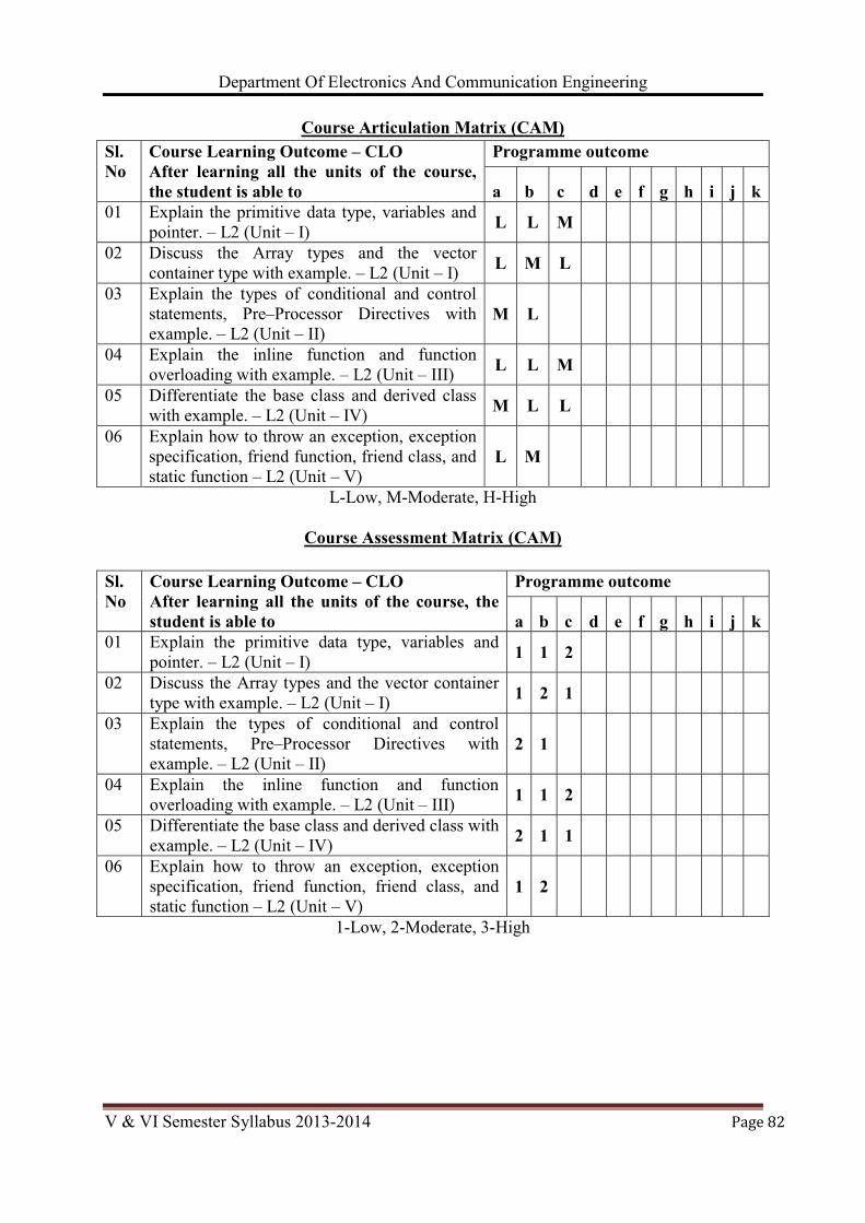
Department Of Electronics And Communication Engineering
V & VI Semester Syllabus 2013-2014 �����������������������������������������������������������������
��
Course Articulation Matrix (CAM)
L-Low, M-Moderate, H-High
Course Assessment Matrix (CAM)
1-Low, 2-Moderate, 3-High
Sl. No
Course Learning Outcome – CLO After learning all the units of the course, the student is able to
Programme outcome
a b c d e f g h i j k01 Explain the primitive data type, variables and
pointer. – L2 (Unit – I) L L M
02 Discuss the Array types and the vector container type with example. – L2 (Unit – I) L M L
03 Explain the types of conditional and control statements, Pre–Processor Directives with example. – L2 (Unit – II)
M L
04 Explain the inline function and function overloading with example. – L2 (Unit – III) L L M
05 Differentiate the base class and derived class with example. – L2 (Unit – IV) M L L
06 Explain how to throw an exception, exception specification, friend function, friend class, and static function – L2 (Unit – V)
L M
Sl. No
Course Learning Outcome – CLO After learning all the units of the course, the student is able to
Programme outcome
a b c d e f g h i j k01 Explain the primitive data type, variables and
pointer. – L2 (Unit – I) 1 1 2
02 Discuss the Array types and the vector container type with example. – L2 (Unit – I) 1 2 1
03 Explain the types of conditional and control statements, Pre–Processor Directives with example. – L2 (Unit – II)
2 1
04 Explain the inline function and function overloading with example. – L2 (Unit – III) 1 1 2
05 Differentiate the base class and derived class with example. – L2 (Unit – IV) 2 1 1
06 Explain how to throw an exception, exception specification, friend function, friend class, and static function – L2 (Unit – V)
1 2

Department Of Electronics And Communication Engineering
V & VI Semester Syllabus 2013-2014 ����������������������������������������������������������������
��
�
Course Title : Radar and Navigational Aids Course Code: P13EC662 Semester : VI L-T-P-H: 2 – 2 – 0-4 Credits:3Contact Period : Lecture :52 Hrs., Exam: 3Hrs. Weightage :CIE:50% SEE:50%
Course Learning Objectives (CLOs)1. Understand the concepts of basics of radar and its applications 2. Derive the radar range equation 3. Discuss the introduction to MTI and pulsed Doppler radar 4. Discuss the digital MTI processing moving target detection and limitations to MTI 5. Explain the about pulsed Doppler radar 6. Understand the concepts of tracking with radar monopulse tracking, conical scan and
sequential lobing 7. Explain the limitations to tracking accuracy, low angle tracking, tracking in range 8. Explain the matched filter receiver, detection criterion and detectors 9. Describe automatic detection, integrators constant and false alarm rate receiver 10. Understand the concepts of various Radar clutters 11. Discuss the reflector antennas, electronically steered phase array antennas 12. Describe the phase shifters and frequency scan arrays 13. Describe the architecture for phased arrays and mechanically steered planar array
antennas 14. Explain the radiation pattern synthesis ,effect of errors on radiation patternsand low side
lobe antennas 15. Understand the concept of radar noise figures, super heterodyne receiver, duplexer and
receiver protectors, radar displays. Course Content
UNIT – I An Introduction to Radar: Basic Radar, Simple form of the Radar equation, Radar block diagram, Radar frequencies, Applications of radar. The Radar equation: Introduction, Detection of signals in noise, Receiver noise and signal to noise ratio, Probabilities of detection and false alarm, Radar cross section of targets, Radar cross section fluctuations. MTI and Pulse Doppler Radar: Introduction, Delay line cancellers, Staggered PRF’s, Text 1: 1.1 to 1.5, 2.1 to 2.3, 2.7, 2.8, 3.1, 3.2, 3.3, 10 Hours
Unit-II MTI and Pulse Doppler Radar: Doppler filter banks, Digital MTI processing, Moving target detection, Limitations to MTI performance MTI from a moving platform(AMTI),Pulse Doppler radar. Tracking Radar: Tracking with Radar, Monopulse tracking, Conical scan and sequential lobing, Limitations to tracking accuracy, Low angle tracking, Tracking in range Text 1: 3.4 to 3.9,4.1 to 4.6 11Hours
Unit-IIIDetection of Signals in Noise: Introduction, Matched filter receiver, Detection criteria, Detectors, Automatic detection, Integrators, Constant false alarm rate receivers. Radar clutter: Introduction to Radar clutter, surface clutter radar equation, land clutter, sea clutter, weather clutter, detection of targets in clutter Text 1: 5.1 to 5.7, 7.1 to 7.4, 7.6, 7.7 10 Hours
Unit-IV The Radar Antenna: Reflector antennas, Electronically steered phases array antennas, Phase shifters, frequency scan arrays, Architectures for phased arrays, Mechanically steered planar
Department Of Electronics And Communication Engineering
V & VI Semester Syllabus 2013-2014 ����������������������������������������������������������������
��
array antennas, Radiation pattern synthesis, Effect of errors on radiation patterns, Low side lobe antennas. Radar receiver: Radar noise figures, Super-heterodyne receiver, Duplexers and receiver protectors, Radar displays. Text 1: 9.4 to 9.7,9.9 to 9.13,11.1 to 11.5 10Hours
Unit-V Radar transmitter:Introduction, linear beam power tubes, solid state RF power sources, cross field amplifiers. Propogation of radar waves: Introduction, Forward scattering from a flat earth,, Scattering from round earth’s surface, Atmospheric refraction-standard propogation, non standard propagation,diffraction, attenuation by atmospheric gases, external or environmental noise Text 1: 10.1 to 10.3, 10.5, 8.1 to 8.8 11Hours
Text Book:1. Introduction to Radar Systems, Merill.I.Skolnik 3rdEdition. Tata McGRAW Hill,2001
Reference Book:1. Elements of Electronic navigation, N.S.Nagaraj, 2nd Edition, Tata McGRAW Hill
RADAR Sytems and Radio aids to Navigations, Dr. A. K sen, A .B Bhattacharya
Lesson PlanUNIT 1
Period No. Topics
1. An Introduction to Radar: Basic Radar 2. Simple form of the Radar equation, Radar block diagram 3. Radar Frequencies, Application of radar 4. The radar equation: Introduction 5. Detect of Signals in noise, Receiver noise and signal to noise ratio 6. Probabilities of detection and false alarm 7. Radar cross section of targets 8. Radar cross section fluctuations 9. MTI and Pulse Doppler Radar: Introduction 10. Delay line cancellers, Staggered PRF’s
UNIT IIPeriod No. Topics
11. MTI and Pulse Doppler Radar: Doppler filter banks 12. Digital MTI processing 13. Moving target detection 14. Limitations to MTI performance MTI from a moving platform(AMTI) 15. Pulse Doppler radar. 16. Tracking Radar: Tracking with Radar 17. Monopulse tracking 18. Conical scan and sequential lobbing 19. Limitations to tracking accuracy 20. Low angle tracking 21. Tracking in range

Department Of Electronics And Communication Engineering
V & VI Semester Syllabus 2013-2014 �����������������������������������������������������������������
��
UNIT IIIPeriod No. Topics
22. Detection of Signals in Noise: Introduction 23. Matched filter receiver 24. Detection criteria 25. Detectors, Automatic detection 26. Integrators, Constant false alarm rate receivers. 27. Radar clutter: Introduction to Radar clutter 28. Surface clutter radar equation 29. Land clutter 30. Sea clutter, Weather clutter 31. Detection of targets in clutter
UNIT IVPeriod No. Topics
32. The Radar Antenna: Reflector antennas 33. Electronically steered phases array antennas 34. Phase shifters, frequency scan arrays, Architectures for phased arrays 35. Mechanically steered planar array antennas 36. Radiation pattern synthesis 37. Effect of errors on radiation patterns 38. Low side lobe antennas. 39. Radar receiver: Radar noise figures 40. Super-heterodyne receiver 41. Duplexers and receiver protectors, Radar displays.
UNIT VPeriod No. Topics
42. Radar transmitter: Introduction 43. Linear beam power tubes 44. Solid state RF power sources, cross field amplifiers. 45. Propagation of radar waves: Introduction 46. Forward scattering from a flat earth 47. Scattering from round earth’s surface 48. Atmospheric refraction-standard propagation 49. Non standard propagation 50. Diffraction 51. Attenuation by atmospheric gases 52. External or environmental noise

Department Of Electronics And Communication Engineering
V & VI Semester Syllabus 2013-2014 �����������������������������������������������������������������
��
Course Title : MULTICORE PROCESSING Course Code: P13EC663 Semester : VI L-T-P-H: 2– 2 – 0-4 Credits: 3Contact Period : Lecture :52 Hrs., Exam: 3Hrs. Weightage :CIE:50% SEE:50%
Course Learning Objectives:1. Discuss the types and significance of threads. 2. Explain the different concepts used in the implementation of parallel programming. 3. Highlight the features of threading API’s for Microsoft Windows and WIN32/MFC. 4. Explain Intel Task queuing Execution model diagram. 5. Discuss the concepts involved in the solutions of Heavily Contended Locks. 6. Discuss the cache related issues with respect to parallel programming
Course ContentUNIT – I
Introduction to Multi– core Architecture: Motivation for Concurrency in software, Parallel Computing Platforms, Parallel Computing in Microprocessors, Differentiating Multi–core Architectures from Hyper– Threading Technology, Multithreading on Single–Core versus Multi–Core Platforms Understanding Performance, Amdahl’s Law, Growing Returns: Gustafson’s Law. System Overview of Threading: Defining Threads, System View of Threads, Threading above the Operating System, Threads inside the OS, Threads inside the Hardware, What Happens When a Thread Is Created, Application Programming Models and Threading, Virtual Environment: VMs and Platforms, Runtime Virtualization, System Virtualization. Text: Chapters 1 and 2 11 Hrs
UNIT – II Fundamental Concepts of Parallel Programming: Designing for Threads, Task Decomposition, Data Decomposition, Data Flow Decomposition, Implications of Different Decompositions, and Challenges You will Face, Parallel Programming Patterns. A Motivating Problem: Error Diffusion, Analysis of the Error Diffusion Algorithm. An Alternate Approach: Parallel Error Diffusion, Other Alternatives. Threading and Parallel Programming Constructs: Synchronization, Critical Sections, Deadlock, Synchronization Primitives, Semaphores, Locks, Condition Variables, Messages, Flow Control–based Concepts, Fence, Barrier, Implementation dependent Threading Features. Text: Chapters 3 and 4 11 Hrs
UNIT – III Threading APIs: Threading APls for Microsoft Windows, Win32/MFC Thread APls, Threading APls for Microsoft Dot–NET Framework, Creating Threads, Managing Threads, Thread Pools, Thread Synchronization, POSIX Threads, Creating Threads, Managing Threads, Thread Synchronization, Signaling, Compilation and Linking. Text: Chapter 5 10 Hrs
UNIT – IV OpenMP: A Portable Solution for Threading Challenges in Threading a Loop, Loop–carried Dependence, Data– race Conditions, Managing Shared and Private Data, Loop Scheduling and Portioning, Effective Use of Reductions, Minimizing Threading Overhead, Work–sharing Sections, Performance– oriented Programming, Using Barrier and No wait, Interleaving Single– thread and Multi– thread Execution, Data Copy–in and Copy–out,

Department Of Electronics And Communication Engineering
V & VI Semester Syllabus 2013-2014 ��������������������������������������������������������������� �
��
Protecting Updates of Shared Variables, Intel Task queuing Extension to OpenMP, OpenMP Library Functions, OpenMP Environment Variables, Compilation, Debugging, performance. Text: Chapter 6 10 Hrs
UNIT – V Solutions to Common Parallel Programming Problems: Too Many Threads, Data Races, Deadlocks, and Live Locks, Deadlock, Heavily Contended Locks, Priority Inversion, Solutions for Heavily Contended Locks, Non–blocking Algorithms, ABA Problem, Cache Line Ping–ponging, Memory Reclamation Problem, Recommendations, Thread–safe Functions and Libraries, Memory Issues, Bandwidth, Working in the Cache, Memory Contention, Cache related Issues, False Sharing, Memory Consistency, Current IA– 32 Architecture, Itanium Architecture, High–level Languages, Avoiding Pipeline Stalls on IA–32, Data Organization for High Performance. Text: Chapter 7 10 Hrs TEXT BOOK: “Multicore Programming”, Increased Performance through Software Multi–threading by Shameem Akhter and Jason Roberts, Intel Press, 2006
REFERENCE BOOKS: 1. “Principles of Parallel Programming”, Calvin Lin, Lawrence Snyder, Pearson Education,
2009. (Listed topics only from Chapters 1, 2, 3). 2. “Parallel Programming in C with MPI and OpenMP”, Michael J. Quinn, Tata McGraw
Hill, 2004. (Listed topics only from Chapters 3, 17).
Course Outcomes:
1. Discuss the types and their flow in execution environment of parallel processing. 2. Describe the types of decomposition and their implications. 3. Outline the steps of error diffusion algorithm. 4. Explain the creation, management and communication among the threads. 5. Differentiate between single thread and multi thread execution. 6. Distinguish between dead locks and live locks.
Department Of Electronics And Communication Engineering
V & VI Semester Syllabus 2013-2014 �����������������������������������������������������������������
��
Course Title : CONTROL SYSTEMS Course Code: P13EC664 Semester : VI L-T-P-H: 2 – 2 – 0-4 Credits:3 Contact Period : Lecture :52 Hrs., Exam: 3Hrs. Weightage : CIE:50% SEE:50%
Course Learning ObjectivesThis course aims to 1. Discuss the mathematical model of physical system, of physical system, mechanical
system and analogous system. 2. Describe the transfer function, block diagram and signal flow graph of different system. 3. Explain the time response specifications, steady state error and error constants. 4. Provide the understanding of the concepts of stability and root locus. 5. Discuss the relative stability using nyquist criteria. 6. Gain the knowledge on the bode plots and its relative stability. 7. Discuss the concepts of state variables and state models for electrical system.
Course ContentUNIT – I
Modeling of Systems: The control system, Mathematical models of physical systems – Introduction, Differential equations of physical systems–Mechanical systems, Friction, Translational systems (Mechanical accelerometer, Levered systems excluded), Rotational systems, Gear trains, Electrical systems, Analogous systems Text: 1.1, 2.1, 2.2, 2.7 10 Hrs
UNIT – II Block diagrams and signal flow graphs: Transfer functions, Block diagram algebra, Signal Flow graphs (State variable formulation excluded)Time Response of feedback control systems: Standard test signals, Unit step response of First and second order systems, Time response specifications, and Time response specifications of second order systems, steady–state errors and error constants. Text: 2.4, 2.5, 2.6, 2.7, 5.1, 5.2, 5.3, 5.4, 5.5 10 Hrs
UNIT – III Stability analysis and Root–Locus Techniques: Concepts of stability, Necessary conditions for Stability, Routh–stability criterion, Relative stability analysis; more on the Routh stability criterion Introduction on route locus techniques, the root locus concepts Construction of root loci. Text: 6.1, 6.2, 6.4, 6.5, 6.6, 7.1, 7.2, 7.3 11 Hrs
UNIT – IV Stability in the frequency domain: Mathematical preliminaries, Nyquist Stability criterion, (Inverse polar plots excluded), Assessment of relative stability using Nyquist criterion, (Systems with transportation lag excluded). Text: 9.1, 9.2, 9.3, 9.4 10 Hrs
UNIT – V Introduction to State variable analysis and Frequency domain analysis: Concepts of state, state variable and state models for electrical systems, Solution of state equations.Introduction on frequency domain analysis, Correlation between time and frequency response, Bode plots, All pass and minimum phase systems, Experimental determination of transfer functions, Assessment of relative stability using Bode Plots. Text: 8.1, 8.2, 8.4, 8.5, 8.6, 12.1, 12.2, 12.3, 12.6 11 Hrs

Department Of Electronics And Communication Engineering
V & VI Semester Syllabus 2013-2014 �����������������������������������������������������������������
��
TEXT BOOK: “Control Systems Engineering”, I. J. Nagarath and M. Gopal, New Age International (P) Limited, Publishers, Fourth edition – 2005
REFERENCE BOOKS: 1. “Modern Control Engineering”, K. Ogata, Pearson Education Asia/ PHI, 4th Edition,
2002. 2. “Concepts of Control Systems”, P. S. Satyanarayana, Dynaram publishers, Bangalore,
2001 3. “Control Systems, Principles and Design”, M. Gopal, TMH, 1999 4. “Feedback control system analysis and synthesis”, J. J. D’Azzo and C. H. Houpis;
McGraw Hill, International student Edition.
Course OutcomeAfter learning all the units of the course, the student is able to 01 Describe the mathematical model of different systems. – L2 (Unit – I) 02 Solve the problems on mechanical system, electrical system & analogous system. – L3
(Unit – I) 03 Explain the block diagram algebra & signal flow graph. – L2 (Unit – II) 04 Discuss the standard test signals, step response and time response of second order system.
– L2 (Unit – II) 05 Describe the steady state error& error constant. – L2 (Unit – II) 06 Explain the concepts of stability & Routh’s criteria. – L2 (Unit – III) 07 Explain the concepts of root locus. – L2 (Unit – III) 08 Discuss the stability using Nyquist criteria. – L2 (Unit – IV) 09 Solve the problems on bode plots. – L3 (Unit – V) 10 Explain the concepts of state & state variables. – L2 (Unit – V)
Topic Learning Outcome After learning all the topics of UNIT – I, the student is able to 01 Describe the mathematical model of physical systems. – L2 02 Describe the Differential equations for physical systems. – L2 03 Explain the concept of Rotational and Translational systems. – L2 04 Explain the concept of Gear trains.-L2 05 Compare Rotational, Translational and electrical systems.-L4
After learning all the topics of UNIT – II, the student is able to 01 Illustrate the transfer functions for different block diagrams. – L3 02 Analyze the concept of signal flow graphs. – L4 03 Describe the Block diagram algebra. – L2 04 Explain the unit step response of the signals. –L2 05 Explain the Time Response of feedback control systems for first and second order
systems. – L2 After learning all the topics of UNIT – III, the student is able to 01 Explain the concept of Stability analysis. – L202 Analyze the Necessary conditions for Stability. – L4 03 Explain the Routh–stability criterion. – L2 04 Explain the concept of relative stability. –L2 05 Explain the concept on root locus techniques. – L2

Department Of Electronics And Communication Engineering
V & VI Semester Syllabus 2013-2014 �����������������������������������������������������������������
��
After learning all the topics of UNIT – IV, the student is able to 01 Explain frequency domain approach.-L2 02 Illustrate the Stability in the frequency domain such as Nyquist criteria. – L3 03 Analyze the Nyquist Stability criterion. – L4 04 Define the Assessment of relative stability using Nyquist criterion. – L1 05 Discuss the steps to construct Nyquist plot.-L2
After learning all the topics of UNIT – V, the student is able to 01 Describe the Frequency domain analysis such as Bode plots and Correlation between
time and frequency response. – L2 02 Analyze the concept of Bode plots. – L4 03 Analyze the relative stability using Bode Plots. – L4 04 Model the “on state variable analysis”. – L4 05 Define the state variable and state models for electrical systems. – L1
Review Questions01. Discuss Laplace transform and transfer function. 02. Solve problems on Transfer function. 03. Distinguish open loop systems and closed loop systems. 04. Describe the mathematical model of physical systems. 05. Describe the Differential equations for physical systems. 06. Explain the concept of Rotational and Translational systems. 07. Explain the concept of Gear trains. 08. Analyze the mechanical systems and electrical systems. 09. Analyze Force-voltage and Force current analogous networks. 10. Compare Rotational, Translational and electrical systems. 11. Illustrate the transfer functions for different block diagrams. 12. Analyze the concept of signal flow graphs. 13. Solve the problems on signal flow graphs. 14. Describe the Block diagram algebra. 15. Compare block diagram and signal flow graph methods. 16. Explain the Time Response of feedback control systems for first and second order
systems. 17. Analyze the concept of Standard test signals. 18. Illustrate the Time response specifications. 19. Define the steady–state errors and error constants.20. Compare standard test signals for type0, type1 & type2. 21. Explain the concept of Stability analysis. 22. Analyze the Necessary conditions for Stability. 23. Explain Hurwitz criterion. 24. Explain the Routh–stability criterion. 25. Analyze different cases of Routh-Hurwitz criterion.26. Discuss the steps to construct root locus. 27. Explain the concept on root locus techniques. 28. Solve problems on root locus techniques. 29. Analyze Graphical method of determining ‘K’ in root locus. 30. Discuss addition of poles and zeroes in root locus method. 31. Explain frequency domain approach. 32. Explain concept of encirclement and mapping.

Department Of Electronics And Communication Engineering
V & VI Semester Syllabus 2013-2014 �����������������������������������������������������������������
��
33. Illustrate the Stability in the frequency domain such as Nyquist criteria. 34. Analyze the Nyquist Stability criterion, (Inverse polar plots excluded). 35. Define the Assessment of relative stability using Nyquist criterion. 36. Discuss the steps to construct Nyquist plot. 37. Explain Co-relation between time domain and frequency domain for second order
system. 38. Explain relation between Transfer function and Frequency Response. 39. Describe the Frequency domain analysis such as Bode plots and Correlation between
time and frequency response. 40. Compare the time and frequency response. 41. Discuss the steps to sketch Bode plot. 42. Analyze the concept of Bode plots. 43. Analyze the relative stability using Bode Plots. 44. Model the “on state variable analysis”. 45. Define the state variable and state models for electrical systems. 46. Solve the problems on state equations. 47. Calculate Transfer function from Magnitude plot. 48. Discuss minimum and non-minimum phase systems. 49. Analyze transfer function from state model. 50. Explain state diagram of standard state model.
Lesson PlanUNIT – I
Period Topics No.
01. Modeling of Systems: The control system. 02. Mathematical models of physical systems – Introduction. 03. Differential equations of physical systems–Mechanical systems. 04. Differential equations of physical systems–Mechanical systems. 05. Friction. 06. Translational systems (Mechanical accelerometer, Levered systems excluded). 07. Rotational systems. 08. Gear trains. 09. Electrical systems. 10. Analogous systems.
UNIT – II Period No. Topics
11. Block diagrams and signal flow graphs: Transfer functions.12. Block diagram algebra.13. Signal Flow graphs (State variable formulation excluded).14. Signal Flow graphs.15. Time Response of feedback control systems: Standard test signals. 16. Unit step response of First and second order systems. 17. Unit step response of First and second order systems. 18. Time response specifications.19. Time response specifications of second order systems. 20. Steady–state errors and error constants.
Department Of Electronics And Communication Engineering
V & VI Semester Syllabus 2013-2014 �����������������������������������������������������������������
��
UNIT – III Period No. Topics
21. Stability analysis and Root–Locus Techniques: Concepts of stability. 22. Concepts of stability. 23. Necessary conditions for Stability. 24. Necessary conditions for Stability. 25. Routh–stability criterion. 26. Routh–stability criterion. 27. Relative stability analysis. 28. Relative stability analysis. 29. More on the Routh stability criterion Introduction on root locus techniques. 30. The root locus concepts Construction of root loci. 31. The root locus concepts Construction of root loci.
UNIT – IV Period No. Topics
32. Stability in the frequency domain: Mathematical preliminaries. 33. Stability in the frequency domain: Mathematical preliminaries. 34. Mathematical preliminaries. 35. Nyquist Stability criterion, (Inverse polar plots excluded). 36. Nyquist Stability criterion, (Inverse polar plots excluded). 37. Nyquist Stability criterion, (Inverse polar plots excluded). 38. Assessment of relative stability using Nyquist criterion, (Systems with transportation lag
excluded). 39. Assessment of relative stability using Nyquist criterion. 40. Assessment of relative stability using Nyquist criterion, (Systems with transportation lag
excluded). 41. Assessment of relative stability using Nyquist criterion, (Systems with transportation lag
excluded).
UNIT – V Period No. Topics
42. Introduction to State variable analysis and Frequency domain analysis: 43. Concepts of state, state variable and state models for electrical systems. 44. Solution of state equations.45. Introduction on frequency domain analysis. 46. Correlation between time and frequency response. 47. Correlation between time and frequency response. 48. Bode plots. 49. All pass and minimum phase systems. 50. Experimental determination of transfer functions. 51. Assessment of relative stability using Bode Plots. 52. Assessment of relative stability using Bode Plots.

Department Of Electronics And Communication Engineering
V & VI Semester Syllabus 2013-2014 ����������������������������������������������������������������
��
Course Articulation Matrix (CAM)
L-Low, M-Moderate, H-High Course Assessment Matrix (CAM)
1-Low, 2-Moderate, 3-High
Sl. No
Course Learning Outcome – CLO After learning all the units of the course, the student is able to
Programme outcome
a b c d e f g h i j k 01 Describe the mathematical model of different systems.
– L2 (Unit – I) L L M
02 Solve the problems on mechanical system, electrical system & analogous system. – L3 (Unit – I) L M H
03 Explain the block diagram algebra & signal flow graph. – L2 (Unit – II) L M M
04 Discuss the standard test signals, step response and time response of second order system. – L2 (Unit – II) L L M
05 Describe the steady state error& error constant. – L2 (Unit – II) L L L
06 Explain the concepts of stability & Routh’S criteria. – L2 (Unit – III) L M H
07 Explain the concepts of root locus. – L2 (Unit – III) L H H 08 Discuss the stability using Nyquist criteria. – L2 (Unit
– IV) L M M
09 Solve the problems on bode plots. – L3 (Unit – V) L M H 10 Explain the concepts of state & state variables. – L2
(Unit – V) L L M
Sl. No
Course Learning Outcome – CLO After learning all the units of the course, the student is able to
Programme outcome
a b c d e f g h i j k01 Describe the mathematical model of different systems. –
L2 (Unit – I) 1 1 2
02 Solve the problems on mechanical system, electrical system & analogous system. – L3 (Unit – I) 1 2 3
03 Explain the block diagram algebra & signal flow graph. – L2 (Unit – II) 1 2 2
04 Discuss the standard test signals, step response and time response of second order system. – L2 (Unit – II) 1 1 2
05 Describe the steady state error& error constant. – L2 (Unit – II) 1 1 1
06 Explain the concepts of stability & Routh’S criteria. – L2 (Unit – III) 1 2 3
07 Explain the concepts of root locus. – L2 (Unit – III) 1 3 3
08 Discuss the stability using Nyquist criteria. – L2 (Unit – IV) 1 2 2
09 Solve the problems on bode plots. – L3 (Unit – V) 1 2 3 10 Explain the concepts of state & state variables. – L2 (Unit
– V) 1 1 2
Department Of Electronics And Communication Engineering
V & VI Semester Syllabus 2013-2014 ����������������������������������������������������������������
��
Course Title : VERILOG HDL LABORATORY Course Code: P13ECL67 Semester : VI L-T-P-H: 0 – 0 – 3-3 Credits:1.5 Contact Period : Lecture :39 Hrs., Exam: 3Hrs. Weightage :CIE:50% SEE:50%
Course Learning Objectives (CLOs)This course aims to 1. Provide the basic knowledge of how to use Xilinx tool and Model SIM. 2. Execute the Verilog code to realize all basic gates. 3. Execute the Verilog code for combinational logic circuit. 4. Execute the Verilog code to describe the functions of a Full Adder. 5. Develop the Verilog code model for 32 bit ALU using the schematic diagram. 6. Develop the Verilog code for the different flip–flops. 7. Design the different types of counter using Verilog Code. 8. Develop the Verilog code to interface seven segment display and LCD and accepting the
hex key pad. 9. Develop the Verilog code to interface of DC and Stepper motor. 10. Develop the Verilog code to generate different waveforms using DAC. 11. Develop the Verilog code to simulate Elevator operations. 12. Develop the Verilog code to control external lights using relays.
Course ContentNote: Programming can be done using any compiler. Download the programs on a FPGA/CPLD boards such as Apex/ Acex/ Max/ Spartan/ Sinfi/ TK Base or equivalent and performance testing may be done using 32 channel pattern generator and logic analyzer apart from verification by simulation with tools such as Altera/ Modelsim or equivalent.
A. EXPERIMENTS: PROGRAMMING (Using Verilog only) 1. Demonstrate the Fundamental knowledge to use Xilinx tool and Model SIM. 2. Write VERILOG HDL code to realize all the logic gates. 3. Write a VERILOG HDL program for the following combinational designs a. 2 to 4 decoder b. 8 to 3 (encoder without priority & with priority) c. 8 to 1 multiplexer d. 4 bit binary to gray converter e. Multiplexer, De –Multiplexer, comparator. 4. Write a VERILOG HDL code to describe the functions of a Full Adder Using three
Modeling styles. 5. Write a model for 32 bit ALU using the schematic diagram shown below
A (31:0), B (31:0), Out (31:0) ALU should use combinational logic to calculate an output based on the four bit op–code input. ALU should pass the result to the out bus when enable line in high, and tri–state the out bus when the enable line is low. ALU should decode the 4 bit op–code according to the given in example below. OPCODE ALU OPERATION A + B A – B A Complement

Department Of Electronics And Communication Engineering
V & VI Semester Syllabus 2013-2014 �����������������������������������������������������������������
��
A * B A AND B A OR B A NAND B
A XOR B 6. Develop the VERILOG HDL code for the following flip– flops, SR, D, JK and T. 7. Design 4 bit binary, BCD counters (Synchronous reset and Asynchronous reset) and “any
sequence” counters.
B. EXPERIMENTS: INTERFACING
1. Write VERILOG HDL code to display messages on the given seven segment display and LCD and accepting Hex key pad input data.
2. Write VERILOG HDL code to control speed, direction of DC and Stepper motor. 3. Write VERILOG HDL code to accept 8 channel Analog signals, Temperature sensors and
display the data on LCD panel or seven segment display. 4. Write VERILOG HDL code to generate different waveforms (Sine, Square, Triangle,
Ramp etc.,) using DAC change the frequency and amplitude. 5. Write VERILOG HDL code to simulate Elevator operations. 6. Write VERILOG HDL code to control external lights using relays.
Course Outcome
After conducting all the experiments the student is able to 01 Demonstrate the Fundamental knowledge to use Xilinx tool and Model SIM –L3 02 Write the Verilog code for all basic gates. – L3 03 Write the Verilog code for combinational logic circuit. – L3 04 Write the Verilog code to describe the functions of a Full Adder Using three modeling
styles. – L3 05 Design the model for 32 bit ALU using the schematic diagram to perform the arithmetic
and logic operation using Verilog code. – L5 06 Analyze the waveforms of RS, JK, D, and T flip– flops. – L4 07 Design the synchronous and asynchronous counter using Verilog Code. – L5 08 Write the Verilog code to Interface seven segment display, LCD and Hex key pad to
FPGA kit using Verilog code. – L3. 09 Write the Verilog code to Interface of DC and Stepper motor to FPGA kit using Verilog
code to control its speed. – L3 10 Write the Verilog code to Interface DAC to FPGA kit using Verilog code to generate
sine, square, triangle, and ramp waveforms. – L3 11 Write the Verilog code to simulate Elevator operations. – L3 12 Write the Verilog code to control external lights using relays. – L3

Department Of Electronics And Communication Engineering
V & VI Semester Syllabus 2013-2014 �����������������������������������������������������������������
��
Course Articulation Matrix (CAM)
L-Low, M-Moderate, H-High
Sl. No
Course Learning Outcome – CLO After conducting all the experiments, the student is able to
Program outcome a b c d e f g h i j k
01 Demonstrate the Fundamental knowledge to use Xilinx tool and Model SIM
L3M M
02 Write the Verilog code for all basic gates. –
L3 M H
03 Write the Verilog code for combinational logic circuit.
L3M H
04 Write the Verilog code to describe the functions of a Full Adder Using three modeling styles. –
L3M H
05 Design the model for 32 bit ALU using the schematic diagram to perform the arithmetic and logic operation using Verilog code. –
L5
L M H
06 Analyze the waveforms of RS, JK, D, and T flip– flops. –
L4 L M H
07 Design the synchronous and asynchronous counter using Verilog Code. –
L5L M H
08 Write the Verilog code to Interface seven segment display, LCD and Hex key pad to FPGA kit using Verilog code. –
L3M H
09 Write the Verilog code to Interface of DC and Stepper motor to FPGA kit using Verilog code to control its speed. –
L3M H
10 Write the Verilog code to Interface DAC to FPGA kit using Verilog code to generate sine, square, triangle, and ramp waveforms. –
L3
M H
11 Write the Verilog code to simulate Elevator operations. –
L3 M H
12 Write the Verilog code to control external lights using relays. –
L3 M H

Department Of Electronics And Communication Engineering
V & VI Semester Syllabus 2013-2014 ��������������������������������������������������������������� �
��
Course Assessment Matrix (CAM)
1-Low, 2-Moderate, 3-High
Sl. No
Course Learning Outcome – CLO After conducting all the experiments, the student is able to
Program outcome a b c d e f g h i j k
01 Demonstrate the Fundamental knowledge to use Xilinx tool and Model SIM
L3 2 2
02 Write the Verilog code for all basic gates. L3 2 3
03 Write the Verilog code for combinational logic circuit.
L32 3
04 Write the Verilog code to describe the functions of a Full Adder Using three modeling styles. –
L32 3
05 Design the model for 32 bit ALU using the schematic diagram to perform the arithmetic and logic operation using Verilog code. –
L5
1 2 3
06 Analyze the waveforms of RS, JK, D, and T flip– flops. –
L4 1 2 3
07 Design the synchronous and asynchronous counter using Verilog Code. –
L5 1 2 3
08 Write the Verilog code to Interface seven segment display, LCD and Hex key pad to FPGA kit using Verilog code. –
L32 3
09 Write the Verilog code to Interface of DC and Stepper motor to FPGA kit using Verilog code to control its speed. –
L32 3
10 Write the Verilog code to Interface DAC to FPGA kit using Verilog code to generate sine, square, triangle, and ramp waveforms. –
L3
2 3
11 Write the Verilog code to simulate Elevator operations. –
L3 2 3
12 Write the Verilog code to control external lights using relays. –
L3 2 3
Department Of Electronics And Communication Engineering
V & VI Semester Syllabus 2013-2014 �����������������������������������������������������������������
��
�
Course Title : DIGITAL COMMUNICATION AND MICROWAVE LABORATORY Course Code: P13ECL68 Semester : VI L-T-P-H: 0 – 0 – 3-3 Credits:1.5 Contact Period : Lecture :39 Hrs., Exam: 3Hrs. Weightage :CIE:50% SEE:50%
Course Learning Objectives (CLOs)This course aims to 1. Provide the basic practical knowledge of digital modulation, demodulation, microwave,
micro–strip–line applications. 2. Know the working of ASK, FSK, PSK, DPSK, QPSK Generation and its detection. 3. Analyze the working o TDM with pulse amplitude modulation and demodulation. 4. Demonstrate the Measurement of frequency, guide wavelength, power, VSWR and
attenuation in a microwave test bench using klystron/ Gunn oscillator as source. 5. Analyze the coupling and isolation characteristics of a micro–strip–line directional
coupler. Course Content
1. ASK , FSK and PSK, and generation and detection of two band limited signals. 2. DPSK generation and detection 3. QPSK generation and detection 4. TDM with pulse amplitude modulation and demodulation (Exp. 1–3 using kit version). 5. Measurement of frequency, guide wavelength, power, VSWR and attenuation in a
microwave test bench 6. Measurement of VSWR, Isolation and coupling factor of Magic Tee. 7. Measurement of directivity of micro–strip Yagi antenna (printed- E – Plane and H-Plane). 8. Measurement of gain of micro–strip Yagi antenna (printed- E – Plane and H-Plane). 9. Determination of coupling and isolation characteristics of a micro–strip directional
coupler. 10. Measurement of resonance characteristics of a micro– strip ring resonator and
determination of dielectric constant of the substrate. 11. Measurement of power division and isolation characteristics of a micro–strip 3 dB power
divider. 12. To simulate QPSK transmitter and receiver taking into account the phase and the
frequency offset. (Using WICOMM–T Kit). 13. To understand the basic aspects of DS–CDMA in single user case and two user case.
(Using WICOMM–T Kit). REFERENCE BOOK: “Advanced Digital Communication Laboratory Manual”, Preetha Sharan, R Bhargava Rama Gowd, CBS Publishers & Distributors Pvt.Ltd., First Edition, 2013.
Course Outcome After conducting all the experiments the student is able to
1. Demonstrate the working of ASK, FSK, PSK, DPSK, QPSK Generation & its detection.-L3 2. Demonstrate the working o TDM with pulse amplitude modulation and de–modulation.- L3 3. Demonstrate the Measurement of frequency, guide wavelength, power, VSWR and attenuation
in a microwave test bench using klystron/Gunn oscillator as source. – L3 4. Demonstrate the coupling and isolation characteristics of a micro–strip directional coupler. -
L3 5. Test the QPSK transmitter and receiver taking into account the phase and the frequency offset.
– L4 6. Test the basic aspects of DS–CDMA in single user case and two user case. – L4
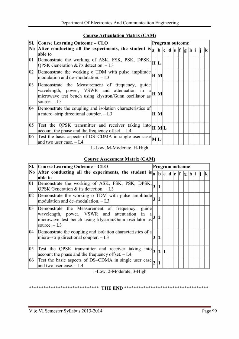
Department Of Electronics And Communication Engineering
V & VI Semester Syllabus 2013-2014 �����������������������������������������������������������������
��
Course Articulation Matrix (CAM)
L-Low, M-Moderate, H-High
Course Assessment Matrix (CAM)
1-Low, 2-Moderate, 3-High
***************************** THE END ***********************************
Sl. No
Course Learning Outcome – CLO After conducting all the experiments, the student is able to
Program outcomea b c d e f g h i j k
01 Demonstrate the working of ASK, FSK, PSK, DPSK,QPSK Generation & its detection. – L3 H L
02 Demonstrate the working o TDM with pulse amplitudemodulation and de–modulation. – L3 H M
03 Demonstrate the Measurement of frequency, guidewavelength, power, VSWR and attenuation in amicrowave test bench using klystron/Gunn oscillator assource. – L3
H M
04 Demonstrate the coupling and isolation characteristics ofa micro–strip directional coupler. – L3 H M
05 Test the QPSK transmitter and receiver taking intoaccount the phase and the frequency offset. – L4 H M L
06 Test the basic aspects of DS–CDMA in single user caseand two user case. – L4 M L
Sl. No
Course Learning Outcome – CLO After conducting all the experiments, the student is able to
Program outcomea b c d e f g h i j k
01 Demonstrate the working of ASK, FSK, PSK, DPSK,QPSK Generation & its detection. – L3 3 1
02 Demonstrate the working o TDM with pulse amplitudemodulation and de–modulation. – L3 3 2
03 Demonstrate the Measurement of frequency, guidewavelength, power, VSWR and attenuation in amicrowave test bench using klystron/Gunn oscillator assource. – L3
3 2
04 Demonstrate the coupling and isolation characteristics of amicro–strip directional coupler. – L3 3 2
05 Test the QPSK transmitter and receiver taking intoaccount the phase and the frequency offset. – L4 3 2 1
06 Test the basic aspects of DS–CDMA in single user caseand two user case. – L4 2 1


![Revised Syllabus for B. Sc. Part III [Mathematics] (Sem. V & VI) to be](https://img.pdfslide.us/doc/110x75/586b769c1a28ab6d678bde24/revised-syllabus-for-b-sc-part-iii-mathematics-sem-v-vi-to-be-.jpg)