Embed Size (px)
Citation preview

8/13/2019 Final Project Report 3
http://slidepdf.com/reader/full/final-project-report-3 1/26
CONTENTS
Receiver Blocks (Details and Schematics)
Receiver SchematicReceiver Waveforms
Transmitter Blocks (Details and Schematics)
Transmitter Schematic
Transmitter Waveforms
8/13/2019 Final Project Report 3
http://slidepdf.com/reader/full/final-project-report-3 2/26
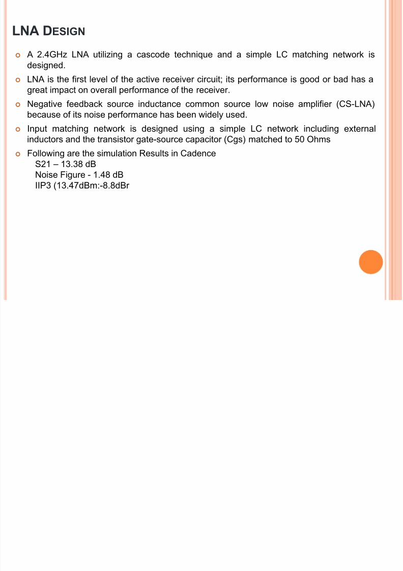
LNA D ESIGN
A 2.4GHz LNA utilizing a cascode technique and a simple LC matching network isdesigned.
LNA is the first level of the active receiver circuit; its performance is good or bad has agreat impact on overall performance of the receiver.
Negative feedback source inductance common source low noise amplifier (CS-LNA)because of its noise performance has been widely used.
Input matching network is designed using a simple LC network including external
inductors and the transistor gate-source capacitor (Cgs) matched to 50 OhmsFollowing are the simulation Results in Cadence
S21 – 13.38 dBNoise Figure - 1.48 dBIIP3 (13.47dBm:-8.8dBr
8/13/2019 Final Project Report 3
http://slidepdf.com/reader/full/final-project-report-3 3/26
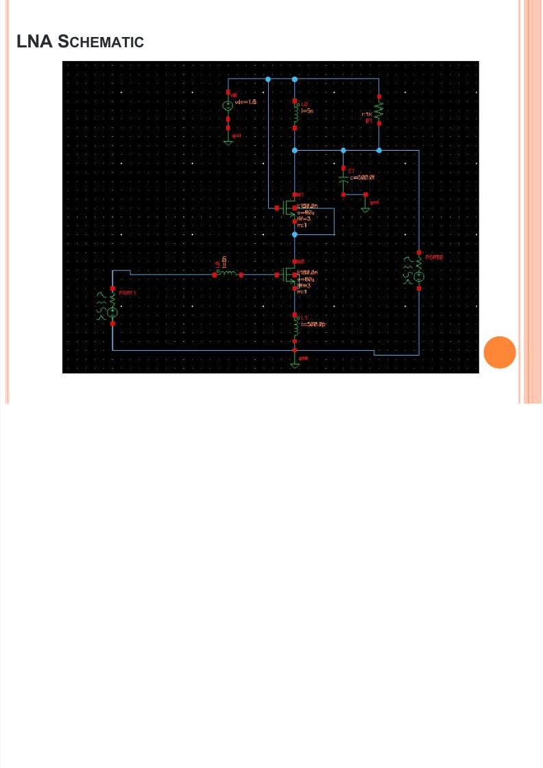
LNA S CHEMATIC
8/13/2019 Final Project Report 3
http://slidepdf.com/reader/full/final-project-report-3 4/26
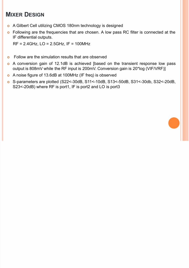
MIXER DESIGN
A Gilbert Cell utilizing CMOS 180nm technology is designed
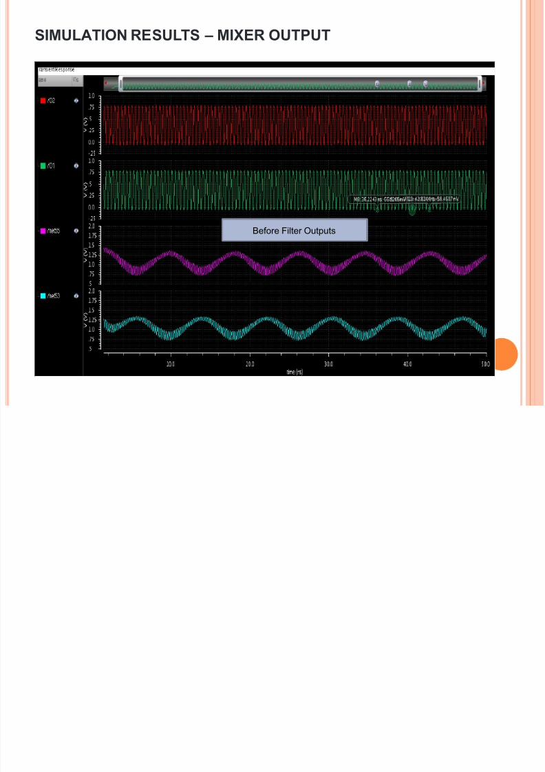
Following are the frequencies that are chosen. A low pass RC filter is connected at theIF differential outputs.
RF = 2.4GHz, LO = 2.5GHz, IF = 100MHz
Follow are the simulation results that are observed
A conversion gain of 12.1dB is achieved [based on the transient response low passoutput is 808mV while the RF input is 200mV. Conversion gain is 20*log (VIF/VRF)]
A noise figure of 13.6dB at 100MHz (IF freq) is observed
S-parameters are plotted (S22<-30dB, S11<-10dB, S13<-50dB, S31<-30db, S32<-20dB,S23<-20dB) where RF is port1, IF is port2 and LO is port3
8/13/2019 Final Project Report 3
http://slidepdf.com/reader/full/final-project-report-3 5/26
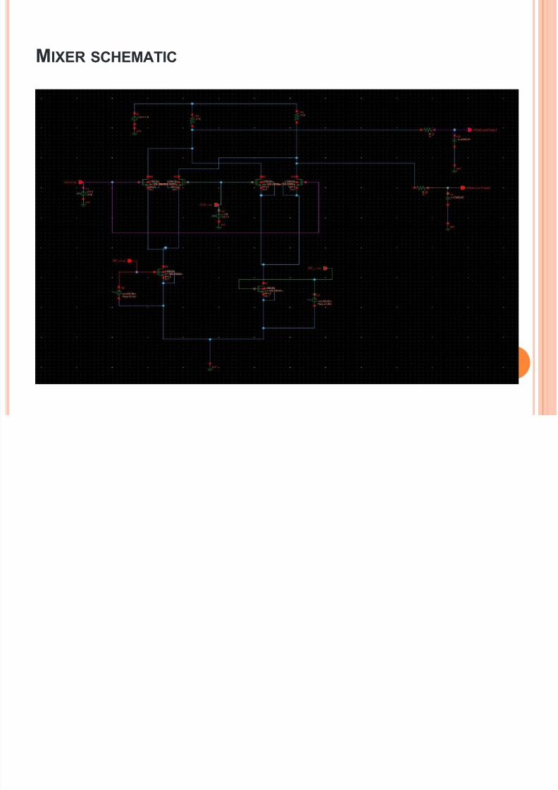
MIXER SCHEMATIC
8/13/2019 Final Project Report 3
http://slidepdf.com/reader/full/final-project-report-3 6/26
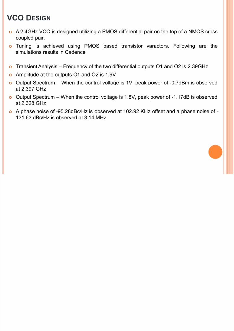
VCO D ESIGN
A 2.4GHz VCO is designed utilizing a PMOS differential pair on the top of a NMOS crosscoupled pair.
Tuning is achieved using PMOS based transistor varactors. Following are thesimulations results in Cadence
Transient Analysis – Frequency of the two differential outputs O1 and O2 is 2.39GHz
Amplitude at the outputs O1 and O2 is 1.9V
Output Spectrum – When the control voltage is 1V, peak power of -0.7dBm is observedat 2.397 GHz
Output Spectrum – When the control voltage is 1.8V, peak power of -1.17dB is observedat 2.328 GHz
A phase noise of -95.28dBc/Hz is observed at 102.92 KHz offset and a phase noise of -131.63 dBc/Hz is observed at 3.14 MHz
8/13/2019 Final Project Report 3
http://slidepdf.com/reader/full/final-project-report-3 7/26
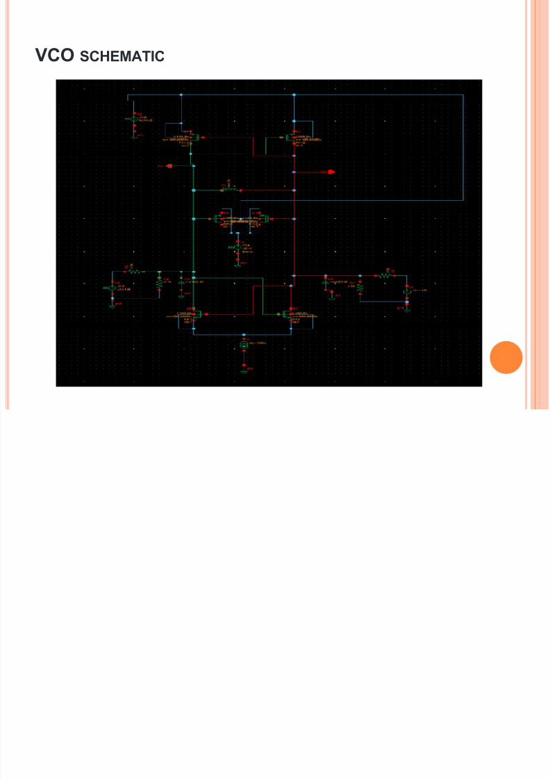
VCO SCHEMATIC

8/13/2019 Final Project Report 3
http://slidepdf.com/reader/full/final-project-report-3 8/26
RECEIVER
8/13/2019 Final Project Report 3
http://slidepdf.com/reader/full/final-project-report-3 9/26
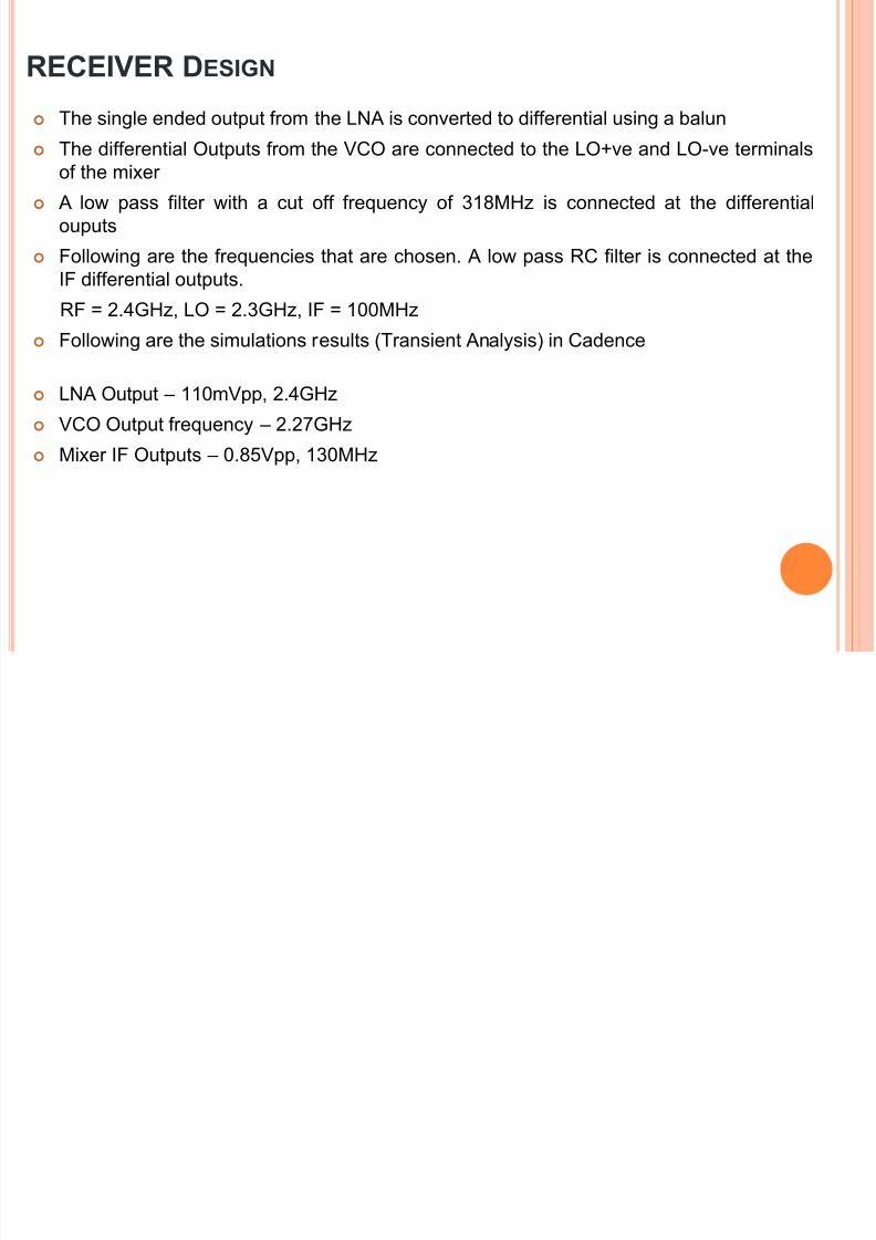
RECEIVER D ESIGN
The single ended output from the LNA is converted to differential using a balun
The differential Outputs from the VCO are connected to the LO+ve and LO-ve terminalsof the mixer
A low pass filter with a cut off frequency of 318MHz is connected at the differentialouputs
Following are the frequencies that are chosen. A low pass RC filter is connected at theIF differential outputs.
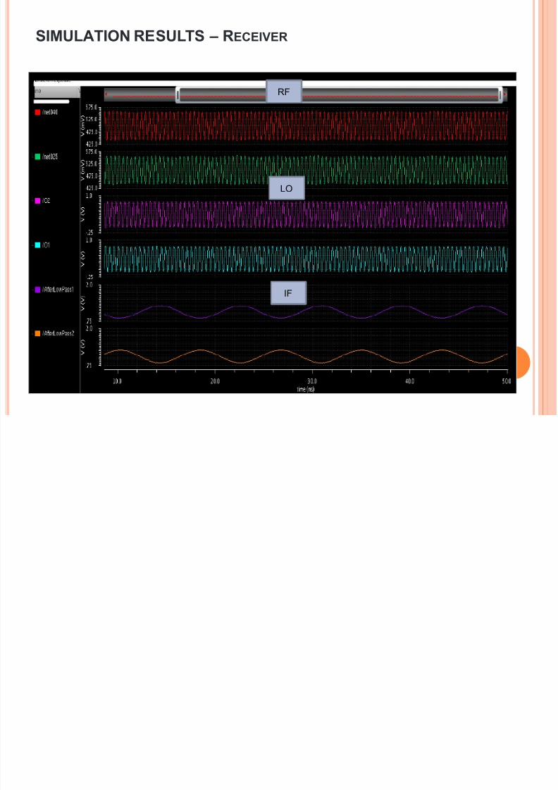
RF = 2.4GHz, LO = 2.3GHz, IF = 100MHzFollowing are the simulations results (Transient Analysis) in Cadence
LNA Output – 110mVpp, 2.4GHz
VCO Output frequency – 2.27GHz
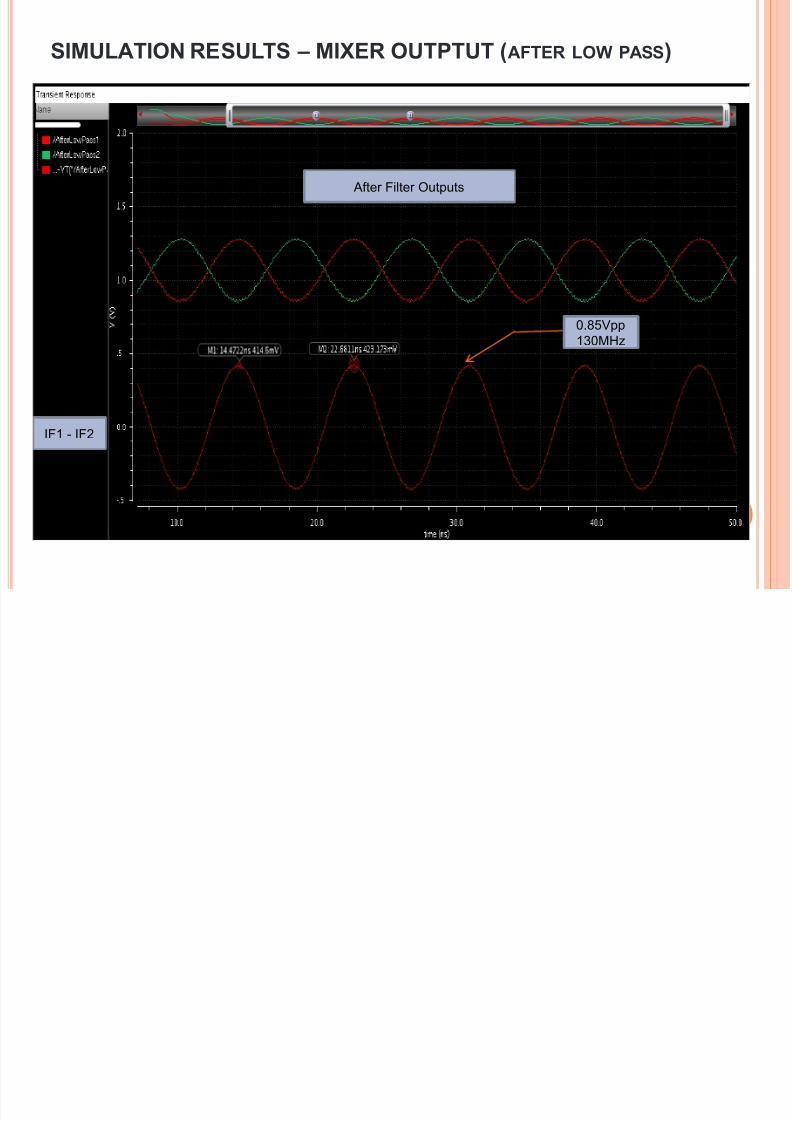
Mixer IF Outputs – 0.85Vpp, 130MHz
8/13/2019 Final Project Report 3
http://slidepdf.com/reader/full/final-project-report-3 10/26
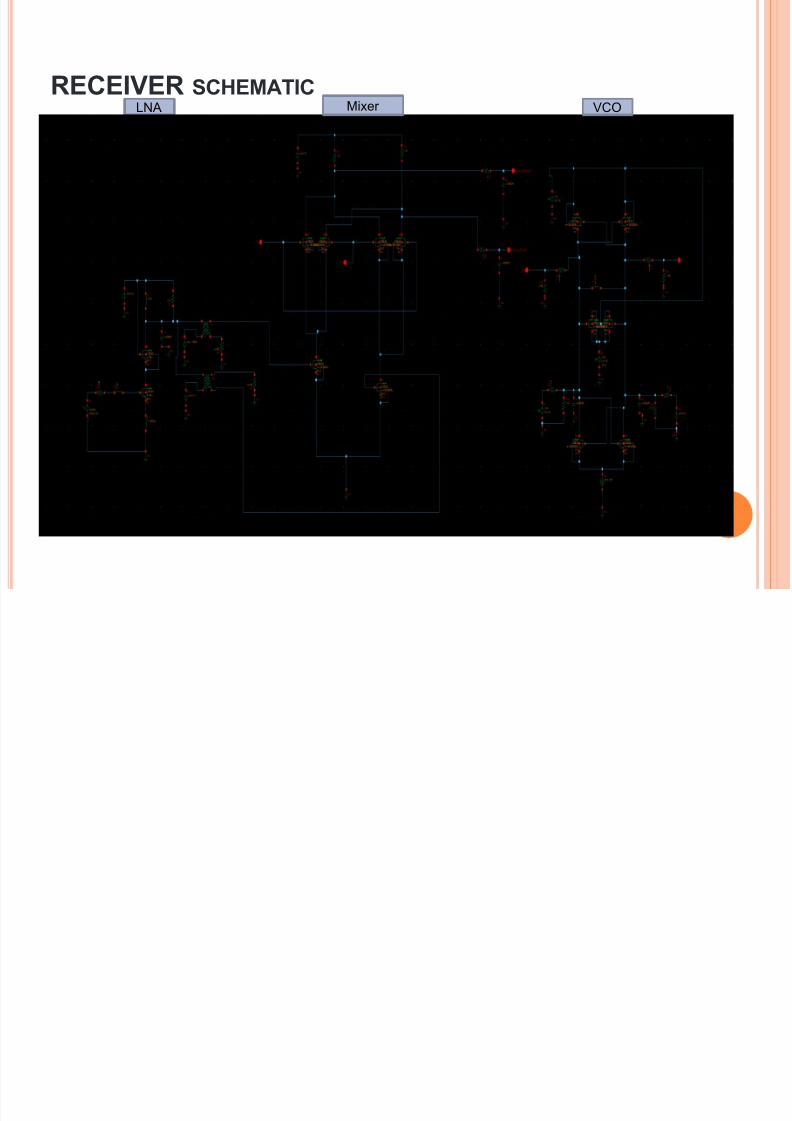
RECEIVER SCHEMATIC LNA Mixer VCO
8/13/2019 Final Project Report 3
http://slidepdf.com/reader/full/final-project-report-3 11/26
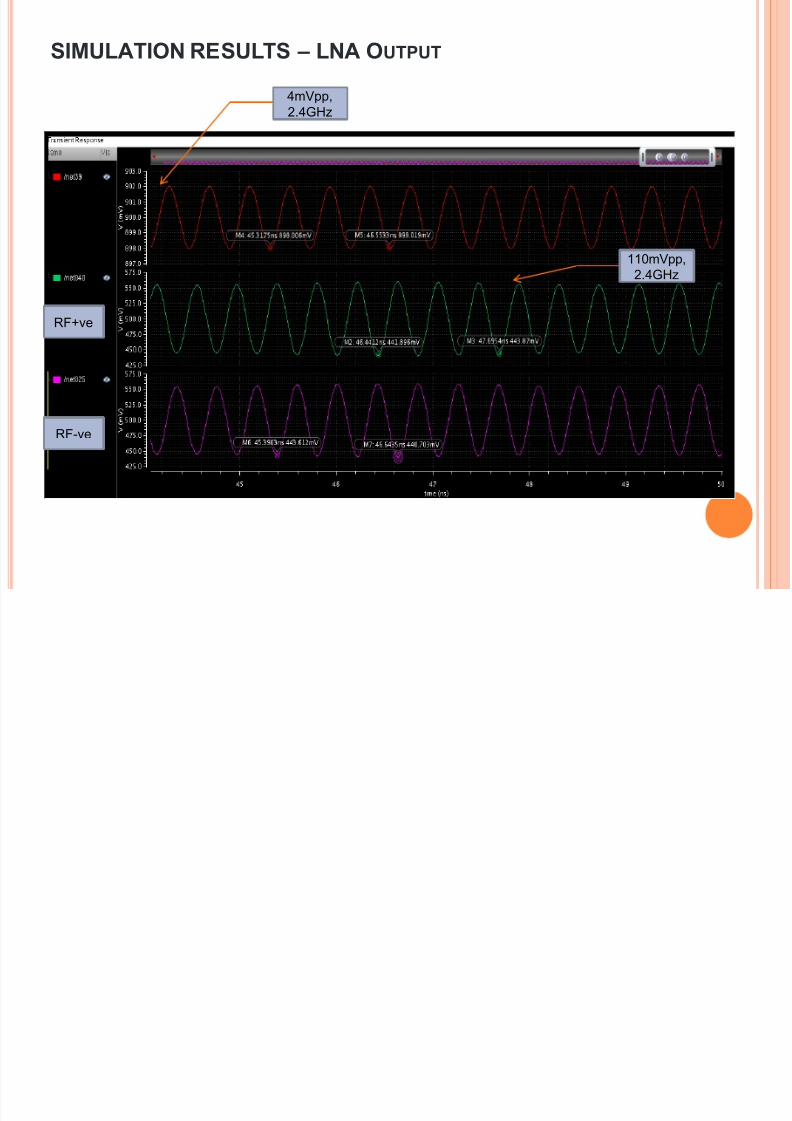
SIMULATION RESULTS – LNA O UTPUT
4mVpp,2.4GHz
RF+ve
RF-ve
110mVpp,
2.4GHz
8/13/2019 Final Project Report 3
http://slidepdf.com/reader/full/final-project-report-3 12/26
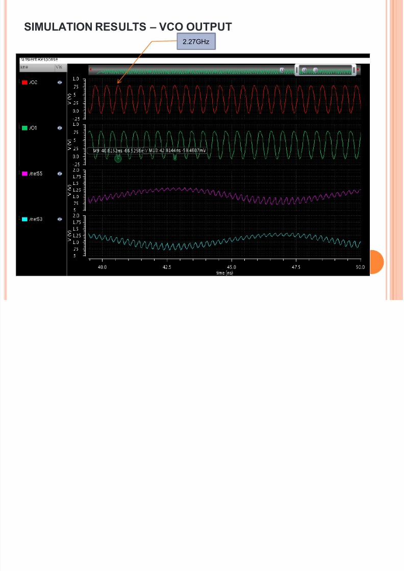
SIMULATION RESULTS – VCO OUTPUT2.27GHz
8/13/2019 Final Project Report 3
http://slidepdf.com/reader/full/final-project-report-3 13/26
SIMULATION RESULTS – MIXER OUTPUT
Before Filter Outputs
8/13/2019 Final Project Report 3
http://slidepdf.com/reader/full/final-project-report-3 14/26
SIMULATION RESULTS – MIXER OUTPTUT ( AFTER LOW PASS )
After Filter Outputs
IF1 - IF2
0.85Vpp130MHz
8/13/2019 Final Project Report 3
http://slidepdf.com/reader/full/final-project-report-3 15/26
SIMULATION RESULTS – R ECEIVER
RF
LO
IF

8/13/2019 Final Project Report 3
http://slidepdf.com/reader/full/final-project-report-3 16/26
TRANSMITTER
8/13/2019 Final Project Report 3
http://slidepdf.com/reader/full/final-project-report-3 17/26
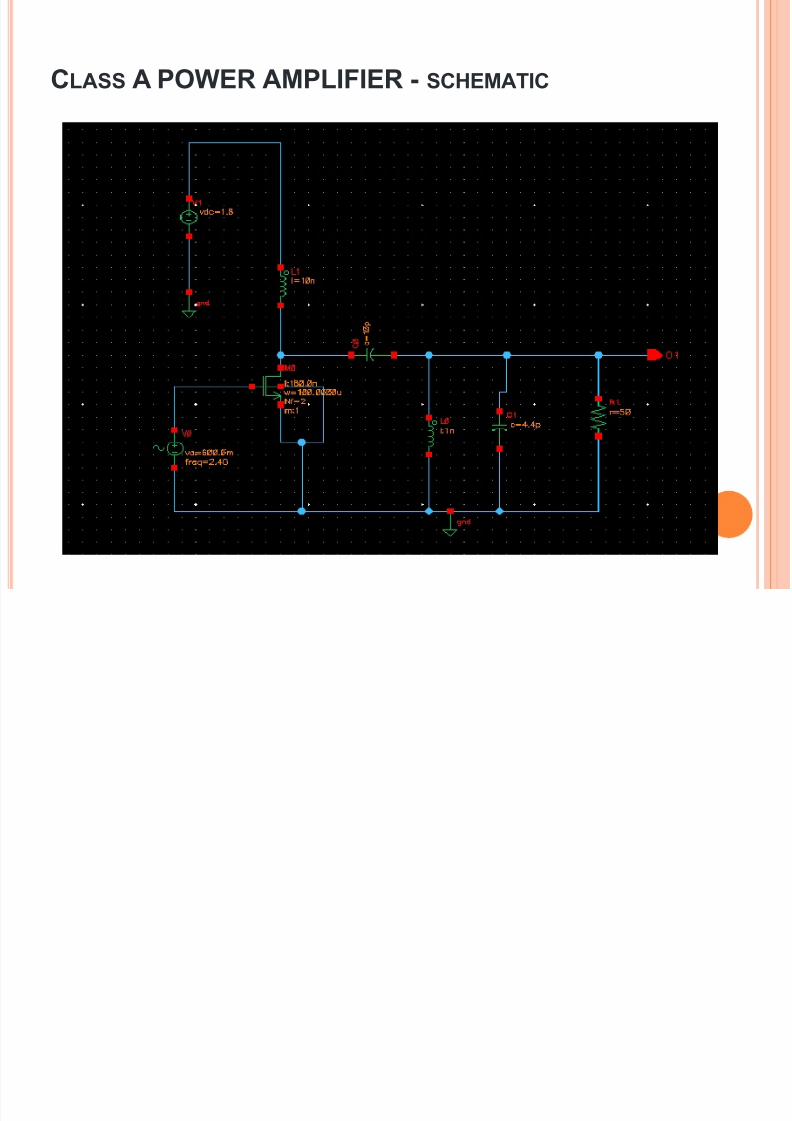
CLASS A POWER AMPLIFIER
Calculations:
Gain = 2.79
Pout = (23.96)*(23.96)*50 = 28.7mW
Pin = 48.2.*1.8 = 86.76mW
Efficiency (n) = Pout/Pin = 33.1%
PN = Pout/(VDSpk*iDmax) = 28.7/(3.55*74.11) = 0.109
Where PN is the normalized output power capability
8/13/2019 Final Project Report 3
http://slidepdf.com/reader/full/final-project-report-3 18/26
CLASS A POWER AMPLIFIER - SCHEMATIC
8/13/2019 Final Project Report 3
http://slidepdf.com/reader/full/final-project-report-3 19/26
TRANSMITTER D ESIGN
The output of the mixer is connected to the Class A power amplifier
The differential Outputs from the VCO are connected to the LO+ve and LO-ve terminalsof the mixer
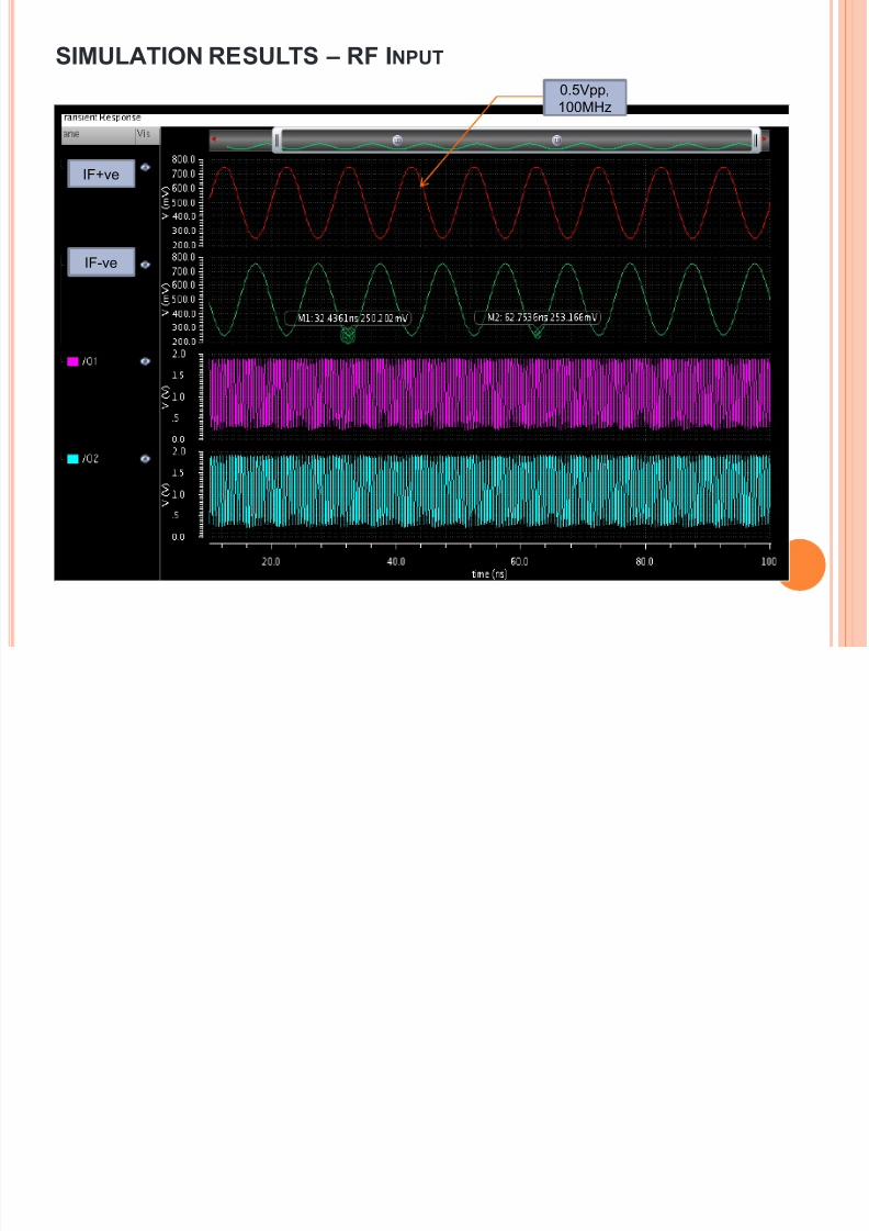
Following are the frequencies that are chosen.
RF = 2.4GHz, LO = 2.3GHz, IF = 100MHz
Following are the simulations results (Transient Analysis) in Cadence
IF inputs – 0.5Vpp, 100MHz
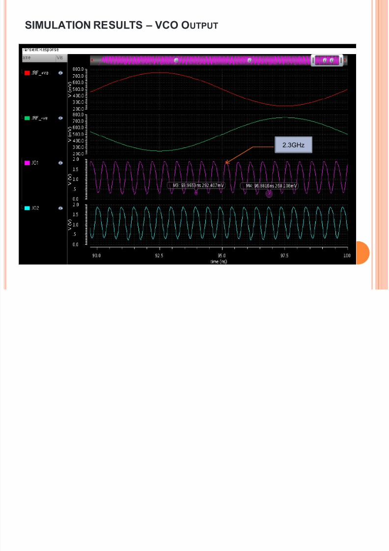
VCO Output frequency – 2.3GHz
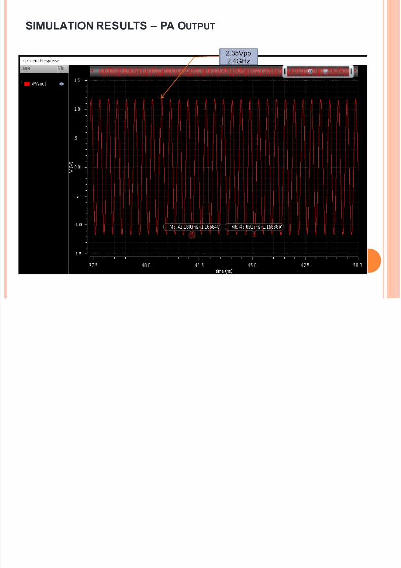
Power Amplifier Output – 2.35Vpp, 2.4GHz
8/13/2019 Final Project Report 3
http://slidepdf.com/reader/full/final-project-report-3 20/26
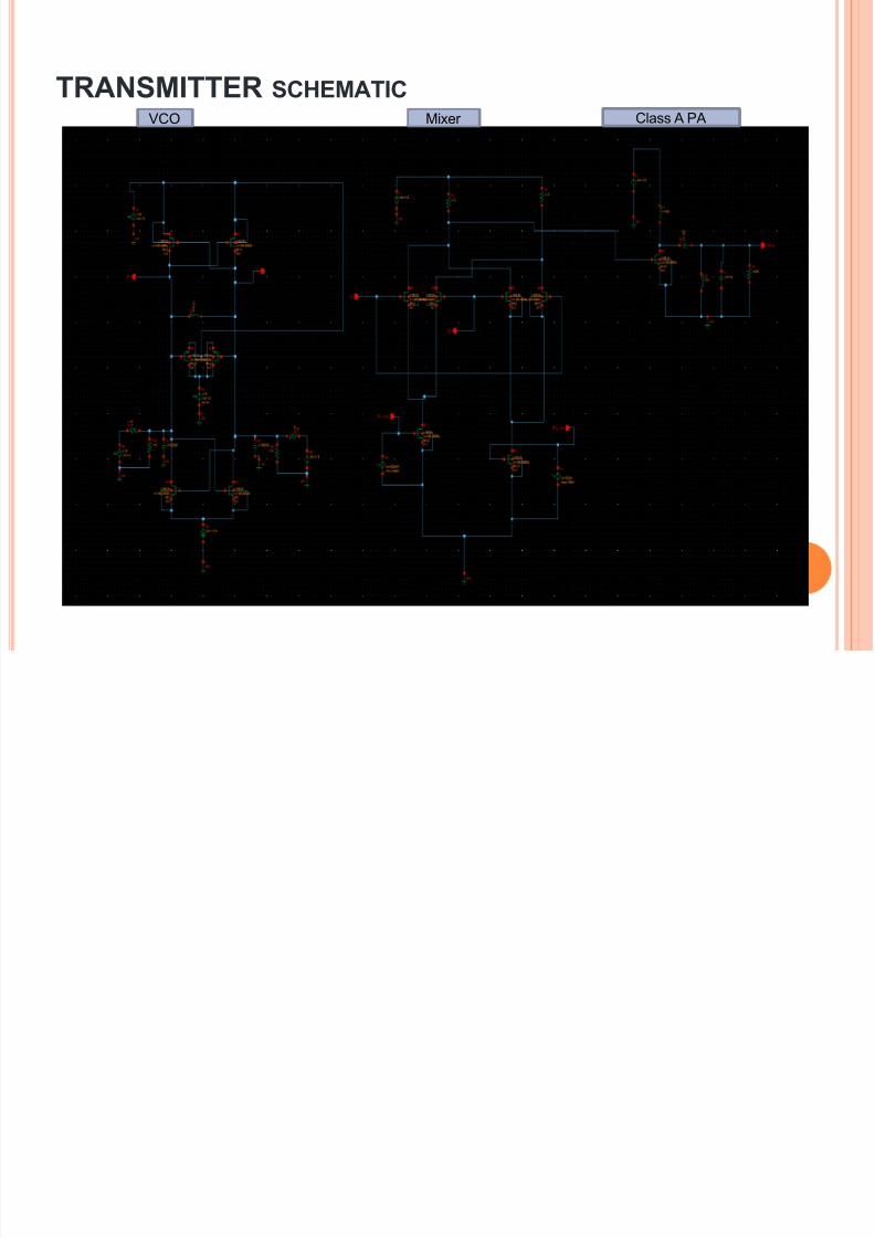
TRANSMITTER SCHEMATIC VCO Mixer Class A PA
8/13/2019 Final Project Report 3
http://slidepdf.com/reader/full/final-project-report-3 21/26
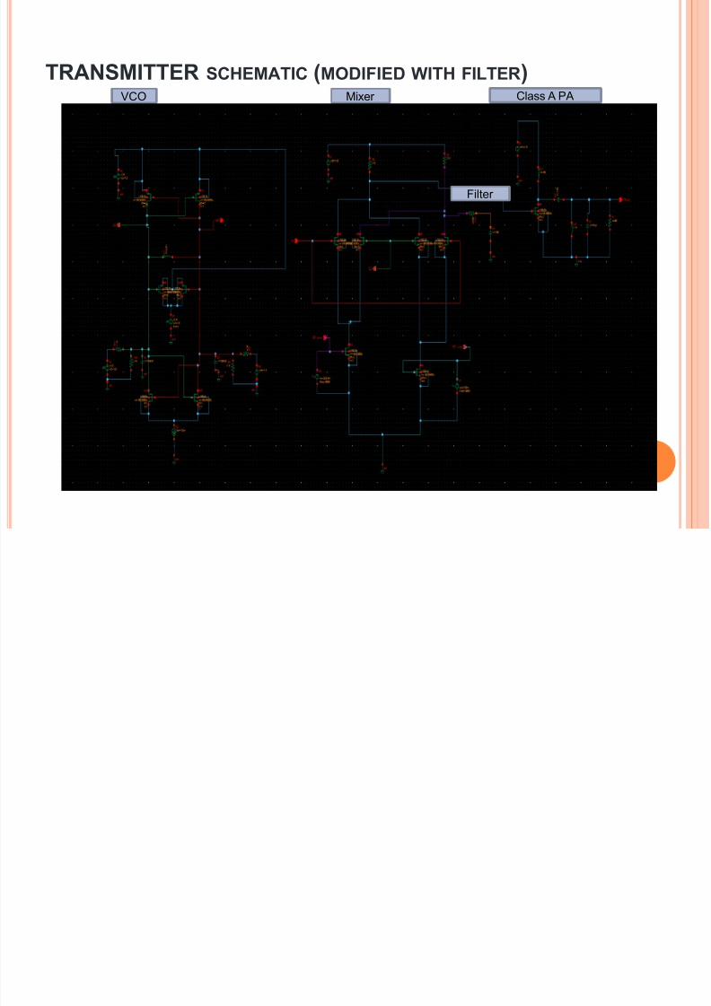
TRANSMITTER SCHEMATIC (MODIFIED WITH FILTER )VCO Mixer Class A PA
Filter
8/13/2019 Final Project Report 3
http://slidepdf.com/reader/full/final-project-report-3 22/26
8/13/2019 Final Project Report 3
http://slidepdf.com/reader/full/final-project-report-3 23/26
SIMULATION RESULTS – VCO O UTPUT
2.3GHz
8/13/2019 Final Project Report 3
http://slidepdf.com/reader/full/final-project-report-3 24/26
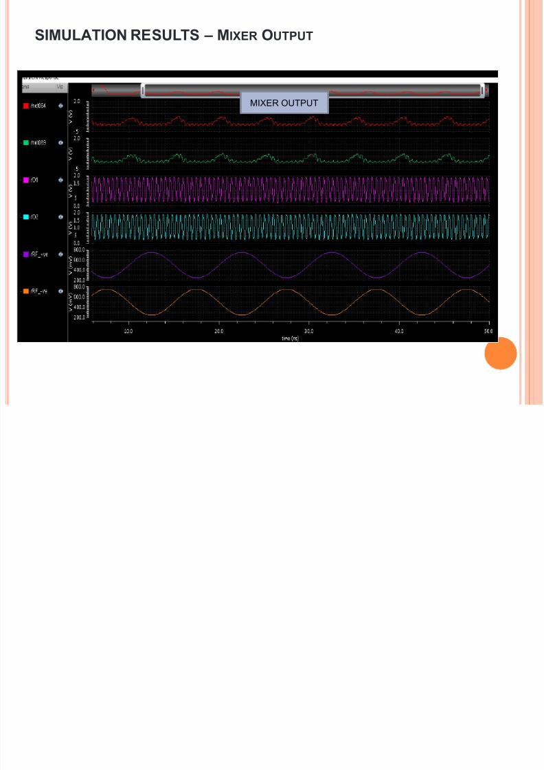
SIMULATION RESULTS – MIXER O UTPUT
MIXER OUTPUT
8/13/2019 Final Project Report 3
http://slidepdf.com/reader/full/final-project-report-3 25/26

8/13/2019 Final Project Report 3
http://slidepdf.com/reader/full/final-project-report-3 26/26
QUESTIONS ???
Thank You