Embed Size (px)
Citation preview

Fa
WD
a
ARRAA
KSSFATA
1
naoeFmfiiatcoong
ta
R
h0
Applied Surface Science 305 (2014) 124–132
Contents lists available at ScienceDirect
Applied Surface Science
journa l h om epa ge: www.elsev ier .com/ locate /apsusc
IM tips in SPM: Apex orientation and temperature considerations ontom transfer and diffusion
illiam Paul ∗,1, David Oliver, Yoichi Miyahara, Peter Grütterepartment of Physics, Faculty of Science, McGill University, Montreal, Canada
r t i c l e i n f o
rticle history:eceived 3 August 2013eceived in revised form 4 February 2014ccepted 1 March 2014vailable online 15 March 2014
a b s t r a c t
Atoms transferred to W(1 1 1) and W(1 1 0) tip apices from the Au(1 1 1) surface during tunneling andapproach to mechanical contact experiments in STM are characterized in FIM at room temperature andat 158 K. The different activation energies for diffusion on the (1 1 1) and (1 1 0) tip planes and the exper-iment temperature are shown to be important factors controlling the extent of changes to the atomicstructure of the tip. W(1 1 1) tips are much better suited to scanning probe studies which require the char-acterization of an atomically defined tip and subsequent verification of its integrity in FIM. The statistics
eywords:canning tunneling microscopycanning probe microscopyield ion microscopytomically defined tips
of the observed spikes in the tunneling current when the tips are approached to Au(1 1 1) are interpretedusing a simple model of adatoms diffusing through the STM junction.
© 2014 Elsevier B.V. All rights reserved.
ip preparationdatom diffusion
. Introduction
The use of tips defined by field ion microscopy (FIM) in scan-ing probe microscopy (SPM) has several notable advantages [1]:n atomically defined tip will pre-define the lateral imaging res-lution, the chemical nature of the apex is guaranteed, and thelectronic structure is calculable based on the known geometry.IM tips offer great potential for the understanding of contrastechanisms in scanning tunneling microscopy (STM) and atomic
orce microscopy (AFM) where the atomic configuration of the tips expected to be of great importance [2], but is usually exper-mentally uncharacterizable. These tips are also well suited fortomic-scale nanoindentation where the tip geometry is neededo understand the initiation of plasticity as well as the electroniconductance of the junction [3,4]. With the recent developmentsf the qPlus [5] and length extension resonators [6] in AFM whichften employ tungsten tips appropriate for FIM [7,8], we expect theumber of instruments using atomically characterized FIM tips torow in the near future.
The implementation of an atomically defined FIM tip in simul-aneous AFM and STM opens up the possibility of performing forcend current characterization of an atomically defined nanojunction,
∗ Corresponding author.E-mail address: [email protected] (W. Paul).
1 Current address: IBM Research Division, Almaden Research Center, 650 Harryoad, San Jose, CA, USA.
ttp://dx.doi.org/10.1016/j.apsusc.2014.03.002169-4332/© 2014 Elsevier B.V. All rights reserved.
perhaps connecting to a single molecule, where the positions ofall relevant atoms are controlled. In a single molecule junction,the exact atomic arrangement of the metallic contacts affectsmetal-molecule coupling, energy-level lineup, and the electro-static potential profile across the junction resulting in considerablechanges to I–V curves [9,10]. To rigorously test and contribute tothe refinement of theoretical modeling of nanoscale structures, oneneeds data from experiments in which the atomic-scale contactgeometry is known and controllable.
In such atomically-defined SPM experiments, tip integrity is ofparamount importance – one must be able to characterize a probeapex in FIM and transfer it to the SPM experiment with certaintythat the atomic arrangement at the end of the tip is unchanged.Tungsten tips are highly reactive and will readily dissociate andchemically bind with gases. Even in ultra-high vacuum conditions,one must be careful to keep impurity gases at bay especially duringand after admission of the FIM imaging gas (usually helium). Thetransfer between imaging modes must also be relatively promptin order to maintain statistical confidence that no rest gases haveadsorbed. This has been a subject of a previous investigation, inwhich we developed the ‘force-field’ method of preserving theatomic integrity of the tip using a large electric field to ionize andrepel any impinging rest gas molecules [11]. This method allowedus to controllably approach an atomically-defined FIM tip to a
cleaved silicon surface in STM and demonstrate its return to FIMwith an unchanged apex.After taking care that the FIM tip does not react with impu-rity gases in the vacuum chamber, one must carefully approach

ace Science 305 (2014) 124–132 125
itettcFmac
ioAatFf
rfpdtdda
iotomol
2
asp1ttwcbA
sapoctaiasdts
fi
111
211
110
(a)
20 nm
(c)
(b)
Fig. 1. (a) Typical W(1 1 1) trimer tip prepared by field evaporation having a radius
W. Paul et al. / Applied Surf
t to the sample surface without overshoot of the feedback con-roller [12]. Finally, tip changes (due to tip-sample interactions, forxample) must be absent from an atomically-defined experimento be assured that the apex structure remains intact. We have notedhat scanning Au(1 1 1) and HOPG surfaces at low tunneling currentonditions (6 pA) at room temperature leads to completely alteredIM tips, while scanning cleaved Si(1 1 1) can be carried out for fewinutes with no detectable tip alterations. The absence of tip alter-
tions in FIM is also correlated with the absence of any tunnelingurrent instabilities (spikes) during the experiment.
Here, we explore tip integrity and the resolvability of tip changesn FIM in greater detail by approaching tips of differing apexrientations (W(1 1 1) and W(1 1 0)) to tunneling proximity withu(1 1 1) surfaces at temperatures of 298 K and 158 K. The tips aredditionally approached to mechanical contact to induce changeso their atomic structure and are subsequently characterized byIM. At both of these temperatures, gold is uncontrollably trans-erred to the tip.
In the case of the W(1 1 1) tip, the transferred atoms can diffuseeadily on the tip surface at room temperature, but do not dif-use when the system is cooled to 158 K. The smooth close-packedlanes of the W(1 1 0) surface, however, still allow the surfaceiffusion of transferred adatoms at 158 K. In contrast to W(1 1 0)ips, W(1 1 1) tips are better suited to SPM studies with atomicallyefined probes because their large surface corrugation hampers theiffusion of transferred atoms and also permits atomic resolutiont the apex region in FIM.
The experimental results presented in this paper are separatednto two main sections: Section 3 presents FIM characterizationf W(1 1 1) and W(1 1 0) tips after tunneling and mechanical con-act experiments with Au(1 1 1) surfaces. In Section 4, the statisticsf tunneling current spikes are interpreted by invoking a simpleodel of a diffusing adatom momentarily altering the conductance
f the STM junction, and we comment on the prospects and chal-enges of using this method for the study of surface diffusion.
. Experimental methods
Experiments were carried out in ultra-high vacuum (UHV)t room temperature and at 158 K (temperature of the tip andample during both FIM and STM). Au(1 1 1) substrates wererepared by epitaxial growth of Au on mica to a thickness of00 nm (these samples were rigidly anchored in order to minimizeip-sample mechanical noise – they were not mounted in the can-ilevered geometry used elsewhere [3,4]). The Au(1 1 1) surfacesere cleaned by repeated 1 keV Ne+ ion sputtering and annealing
ycles in UHV to several cycles beyond the disappearance of car-on in Auger electron spectroscopy. A STM topograph of a cleanu(1 1 1) surface is shown in Fig. 1(c).
Tips were electrochemically etched from polycrystalline tung-ten or single-crystalline W(1 1 1) wire and prepared by flashnnealing and degassing cycles in UHV [13,14]. Tips fabricated fromolycrystalline tungsten wire nearly always terminate with a (1 1 0)riented grain at the apex (to within several degrees) due to therystallographic texture arising from the cold drawing process usedo fabricate the wire [15,16]. Field evaporation was used to prepare
clean tip surface by raising the imaging field by ∼10–20% dur-ng FIM relative to the field required for He+ ion imaging of thepex. The FIM image of a 6.7 ± 0.8 nm radius W(1 1 1) tip apex ishown in Fig. 1(a) with the low-index planes labeled. The radius isetermined by the ring counting method [11,17–19]. The apices of
he W(1 1 1) tips end in three individually resolved atoms (trimer),imilar to the tips described in Ref. [11].After preserving the atomic integrity of the tips using the ‘forceeld’ protocol while UHV conditions recovered following FIM [11],
of 6.7 ± 0.8 nm, imaged at 7.3 kV in FIM; (b) Ball model (side view) of a W(1 1 1) tipand Au(1 1 1) surface; (c) Room temperature STM image of a clean Au(1 1 1) surfaceshowing the herringbone reconstruction (8 pA, −0.95 V sample bias).
the tips were approached to tunneling interaction with Au(1 1 1)samples at a setpoint of 6 pA at −0.08 V sample bias without over-shoot of the tunneling setpoint. The initial coarse approach wasmonitored optically: the tip can be brought to 5–10 �m from thesurface by observing its reflection off the sample, allowing the sam-ple surface to be found less than 30 min after removing the ‘forcefield’ voltage from the tip. Upon finding the sample surface, thetunneling current was recorded at low feedback gain for later anal-ysis. In the case of the W(1 1 0) tips made from polycrystalline wire,soft mechanical indentations were carried out as described in theresults section. FIM was then performed again on the tip apices toexamine modification caused during the tunneling or mechanicalcontacts experiments. The FIM and STM microscopes are combinedinto the same unit which enables the switching of modes withoutany transfer of the tip.
3. Atom transfer to W(1 1 1) and W(1 1 0) tips
3.1. W(1 1 1) tip/Au(1 1 1) surface at 298 K and 158 K
When clean FIM tips are approached to tunneling proximitywith Au(1 1 1) surfaces, spikes are always observed in the tunnel-ing current. At room temperature, the spikes reach a maximumof ∼40 pA, and lead to a completely changed tip structure afterremaining within tunneling proximity of the sample for a fewminutes, as illustrated in Fig. 2(a). The same type of tunnelingexperiment was again performed with the Au(1 1 1) surface butat a temperature of 158 K, as shown in Fig. 2(b). A representativesnapshot of the current trace during tunneling and FIM images ofthe tip structure before and after tunneling are shown. The verti-cal axes of the current traces have the same limits, emphasizingthat the current spikes in the lower-temperature data are muchlarger, reaching ∼130 pA (the larger spike amplitude reflects thelonger residency time of adatoms under the tip at low temperature,discussed in Section 4). The FIM tip retracted from the tunnelingjunction at 158 K appears to have a nearly identical apex, with theexception of an additional atom appearing very brightly next tothe original trimer apex. The lower-right atom in the trimer alsoappears brighter.
The minor modification of the tip apex near the (111) planeprovides two encouraging results: Firstly, the minor tip changeslocated only at the tip apex confirm that the adatoms we observeon the FIM tips after tunneling originate from the sample, not fromthe tip shank. This supports our previous supposition based on
the absence of tip changes when approaching the reactive cleavedSi surface [11]. Secondly, the localized modification demonstratesthat the tip’s (1 1 1) apex is indeed the part of the tip which interactswith the sample – it confirms that the apex is oriented in the correct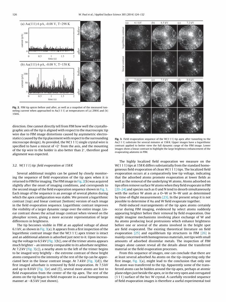
126 W. Paul et al. / Applied Surface Science 305 (2014) 124–132
(a) Au(111) 6 pA, -0.08 V, T=298 K
before
after
time (s)
curr
ent (
pA)
time (s)
curr
ent (
pA)
(b) Au(111) 6 pA, -0.08 V, T=158 K
before
after
6.5 kV
7.3 kV
7.2 kV
6.5 kV
0 0.5 1 1.5 2
0
50
100
0 0.5 1 1.5 2
0
50
100
Fig. 2. FIM tip apices before and after, as well as a snapshot of the measured tun-n1
dgwsmsoa
3
irstEwcitepd
6laimAtacfiafiam
6.1 kV 6.5 kV 7.2 kV
7.4 kV 7.5 kV 8.0 kV
(a) (b) (c)
(d) (e) (f)
loga
rithm
ic c
ontra
stlin
ear c
ontra
stlo
garit
hmic
con
tras t
linea
r con
trast
Fig. 3. Field evaporation sequence of the W(1 1 1) tip apex after tunneling to theAu(1 1 1) substrate for several minutes at 158 K. Upper images have a logarithmic
ferred atoms can be hidden around the tip apex, perhaps at atomic
eling current when approached to Au(1 1 1) at temperatures of (a) 298 K and (b)58 K.
irection. One cannot directly tell from FIM how well the crystallo-raphic axis of the tip is aligned with respect to the macroscopic tipire due to FIM image distortions caused by asymmetric electro-
tatics (caused by the tip placement with respect to the surroundingicroscope design). As provided, the W(1 1 1) single crystal wire is
pecified to have a miscut of <2◦ from the axis, and the mountingf the tip wire to the holder is also better than 2◦, therefore goodlignment was expected.
.2. W(1 1 1) tip: field evaporation at 158 K
Several additional insights can be gained by closely monitor-ng the sequence of field evaporation of the tip apex when it iseturned to FIM for imaging. The FIM image in Fig. 2(b) was acquiredlightly after the onset of imaging conditions, and corresponds tohe second image of the field evaporation sequence shown in Fig. 3.ach image of the sequence is an average of several photos duringhich the apex configuration was stable. We present a logarithmic
ontrast (top) and linear contrast (bottom) version of each imagen the field evaporation sequence. Logarithmic contrast improveshe visibility of a larger dynamic range over the entire image. Lin-ar contrast shows the actual image contrast when viewed on thehosphor screen, giving a more accurate representation of largeifferences in brightness.
The tip becomes visible in FIM at an applied voltage of about.1 kV, as shown in Fig. 3(a). It appears from a first inspection of the
ogarithmic contrast image that the W(1 1 1) apex trimer is intactnd an additional adatom is adsorbed just next to it. Upon increas-ng the voltage to 6.5 kV (Fig. 3(b)), one of the trimer atoms appears
uch brighter – an intensity comparable to its adsorbate neighbor.t 7.2 kV (Fig. 3(c)), a nearby atom to the left of the trimer begins
o be imaged very brightly – the extreme contrast of these brighttoms compared to the intensity of the rest of the tip can be appre-iated best in the linear contrast image. At 7.4 kV (Fig. 3(d)), therst imaged adsorbate is removed by field evaporation. At 7.5 kVnd up to 8.0 kV (Fig. 3(e) and (f)), several more atoms are lost to
eld evaporation from the center of the tip apex. The rest of thetoms on the tip began to field evaporate in a usual homogeneousanner at ∼8.5 kV (not shown).contrast applied to better view the full dynamic range of the FIM image. Lowerimages show a linear contrast to highlight the large brightness enhancement of theevaporating adatoms in FIM.
The highly localized field evaporation we measure on theW(1 1 1) tips at 158 K differs substantially from the standard homo-geneous field evaporation of clean W(1 1 1) tips. The localized fieldevaporation occurs at a comparatively low tip voltage, indicatingthat the adsorbed atoms promote evaporation at lower fields aswell as the removal of the underlying W atoms. Atoms adsorbed ontips often remove surface W atoms when they field evaporate in FIM[20–24] and species such as O and N tend to desorb simultaneouslywith the surface W atom as a O W or N W unit as determinedby time-of-flight measurements [23]. In the present setup it is notpossible to determine if Au and W field evaporate together.
Field-induced rearrangements of the tip apex atoms certainlyoccur during FIM imaging, evidenced by select atoms suddenlyappearing brighter before their removal by field evaporation. Onemight imagine mechanisms involving place exchange of W andAu atoms producing local protrusions which enhance brightnessbefore one or several of the atoms involved in the bright spotare field evaporated. The existing theoretical literature on fieldevaporation [25] and equilibrium tip structures in FIM [26] ismainly concerned with homogeneous materials, not tips with smallamounts of adsorbed dissimilar metals. The inspection of FIMimages alone cannot reveal all the details about the transferredmaterial or the field evaporation processes.
From this sequence of images, one can conclude that there areat least several adsorbed Au atoms on the tip–inspecting only thefirst image, Fig. 3(a), might lead to the conclusion that only oneAu atom was transferred to the tip. Apparently some of the trans-
plane edges just beside the apex, or in the very open and corrugated(1 1 1) surface of the bcc W crystal. A carefully recorded sequenceof field evaporation images is therefore a useful experimental tool

W. Paul et al. / Applied Surface Science 305 (2014) 124–132 127
T = 298 K
T=
8K
15
Fig. 4. Expected RMS displacement of diffused adatoms at T = 158 K and T = 298 Kdpa
tdacc
tbtsmiltnmt
31
wa2t
tbtohbc
d
〈
wfdtaFs
Table 1Activation energies for W, Pd, Ni adatom diffusion on W(1 1 0) and W(1 1 1) surfaces.
Surface/adatom W Pd Ni
W(1 1 0) 0.93 eV 0.51 eV 0.49 eV
uring 1000 s as a function of activation energy. Upper and lower limits of the dis-lacement estimated from FIM data dictate a range for the activation energy fordatoms to escape from the vicinity of the tip apex.
o verify the integrity of the tip apex: If indeed no tip changes occururing STM, no adsorbate promoted field evaporation would occur,nd the field evaporation of the (1 1 1) apex would commence at aomparable field to the rest of the tip structure (∼8.5 kV in thisase).
Another concern regarding the estimation of the number ofransferred atoms is that some fraction of adsorbed atoms will likelye field evaporated at a field lower than that required for ionizinghe He imaging gas in FIM. Bulk Au cannot be imaged in He+ ion FIM,o if a small cluster of Au formed at the tip apex, one would expectany of the bulk-like Au atoms to be removed before the onset of
maging [27,28]. This process might only allow the imaging of theast layer of Au which would be more strongly bonded to the Wip atoms. Certainly, the best way to experimentally determine theumber of transferred atoms and to investigate field evaporationechanisms (whether or not W and Au are evaporated together) is
o implement time-of-flight mass spectrometry.
.3. W(1 1 1) tip: diffusion of transferred atoms on the apex at58 K and 298 K
The contrast in the extent of tip modifications after tunnelingith Au(1 1 1) at room temperature and 158 K is striking. Adatoms
re observed to have diffused over all visible regions of the tip at98 K. At 158 K, however, the modifications are highly localized tohe apex.
The spatial extent of the tip changes observed in FIM at thesewo temperatures allows the estimation of rough upper and lowerounds for the activation energy of Au atoms diffusing over the Wip surface. We note that the diffusion barriers on different planesf the same crystal are in reality very different – what we extractere is an effective energy whose estimation should be dominatedy the largest of the barriers of the relevant planes of the tip (in thisase, the W(1 1 1) plane).
For a particle on a two dimensional surface, the mean squareiffusion distance in time � is
r2〉 = 4�D0 exp(
− Ea
kBT
), (1)
here D0 is a diffusion prefactor (takes into account the attemptrequency and jump distance), Ea is the activation energy of theiffusion jump process, kB is the Boltzmann constant, and T is the
emperature [29,30]. For an experimental delay time of � ≈ 1000 snd assuming a typical prefactor of D0 = 10−3 cm2/s [30], we plot inig. 4 two exponential curves expressing the expected root-mean-quare (RMS) displacement at temperatures of 158 K and 298 K.W(1 1 1) 1.85 eV 1.02 eV 0.87 eV
From Ref. [29].
From the room temperature FIM image in Fig. 2(a), we can esti-mate a lower bound for the RMS displacement of transferred Auadatoms – they are observed essentially ‘everywhere’ on the tip,indicating a RMS displacement greater than 10 nm. This providesan estimate of the upper bound of the effective activation energyfor diffusion of ∼0.74 eV. If the energetic barrier were higher, theadatoms could not have been displaced all over the tip. From theFIM image at 158 K, Fig. 2(b), it appears that the damage to the tipextends to a lateral width of only ∼2–3 nm (atoms on the W(1 1 1)plane are spaced by 0.46 nm). We estimate the lower bound for theactivation energy based on a RMS displacement of 1 nm at 158 Kto be ∼0.46 eV. It is possible that the RMS displacement due toadatom diffusion is actually less than 1 nm: If a cluster of Au formedon the tip apex, the mechanism by which the damage spread to awidth of ∼2–3 nm may not be diffusion of Au on the W tip, but therearrangement of a small Au cluster on the tip as adatoms are col-lected. The suggested activation energy window of 0.46–0.74 eV forgold adatom diffusion on tungsten is of the correct order for metalson tungsten surfaces (see Table 1).
3.4. W(1 1 0) tip/Au(1 1 1) surface at 158 K
In a manner similar to W(1 1 1) tips, tunneling currents mea-sured between W(1 1 0) tips and Au(1 1 1) surfaces also exhibitcontinuous spikes. In FIM, the evidence of transferred atoms ismuch more difficult to discern than for W(1 1 1) tips because oftheir atomic structure made up of smooth planes. We use FIM toexamine changes to the W(1 1 0) tips after approach to mechani-cal contact to Au(1 1 1) at 158 K and after tunneling to Au(1 1 1) at158 K.
Fig. 5 summarizes the first of two experiments in which aW(1 1 0) tip was approached to mechanical contact with theAu(1 1 1) substrate at a temperature of 158 K. The W(1 1 0) tip wasfabricated with polycrystalline tungsten wire, so it is expected thatthe (1 1 0) pole of the apex is aligned to within 10◦ of the wireaxis (estimated from the X-ray diffraction pole figure of the {1 1 0}reflections for cold drawn tungsten wire reported by Greiner andKruse [16]). The tip apex was characterized by FIM before approachto the sample, shown in Fig. 5(a) with the low index planes labeled.
After the initial approach to tunneling proximity with theAu(1 1 1) surface, the tip apex was moved toward the surface toincrementally larger displacements while monitoring the currentbehavior until a signature of mechanical contact was obtained.For small displacements from the tunneling setpoint, a plot ofthe current as a function of tip displacement, I(z), will reveal theexponential distance behavior expected for a tunneling junction.The current recorded upon approach and retraction, ‘in’ and ‘out’directions, should overlap unless there are any major mechanicalchanges occurring in the tip-sample junction. The I(z) curve plottedin Fig. 5(b) shows the exponential increase on the ‘in’ curve (green)with an apparent barrier height of ∼4.7 eV, of the order expected fora clean metal-metal contact [31]. The fit to the data is shown by theblack line from 15 to 200 pA. At ∼10 nA on the ‘in’ curve, an instabil-ity occurs and the junction conductance abruptly increases. Upon
withdrawal of the tip from the sample, a large ∼0.5 nm hysteresisis present, interpreted as the drawing and breaking of a wire of Auatoms pulled up from the sample. After this signature of mechanicalcontact, the tip was returned to FIM for characterization.
128 W. Paul et al. / Applied Surface Science 305 (2014) 124–132
−1.2 −1 −0.8 −0.6 −0.4 −0.2 0 0.2 0.410−12
10−11
10−10
10−9
10−8
10−7
10−6
Depth [nm]C
urre
nt [A
mp]
Bias = −0.1V; φ= 4.65eV
5.2 kV(d)
5.1 kV(a) before
5.4 kV 5.8 kV
4.9 kV
(e)
(b) tip approach to contact
(f)
(c) after
110111
211
in
out
F urve ad roach
iii(slatplt(–t
maaphc
cnaas
ig. 5. (a) FIM image of the ∼12 nm radius W(1 1 0) tip apex. (b) Current–distance cirections. (c)–(f) Field evaporation sequence of the tip imaged in FIM after the app
The FIM imaging sequence after mechanical contact is shownn Fig. 5(c)–(f) during which the imaging voltage was graduallyncreased. In Fig. 5(c), some of the changes to the tip apex arendicated by arrows – a few atoms have adsorbed onto the apex1 1 0) plane, as well as the edge of (1 1 0) planes two to four atomicteps down from the apex. The edges of the (1 1 0) planes, particu-arly the second and third atomic steps down from the (1 1 0) pole,ppear disordered, indicating changes to the atomic structure atheir edges. Changes to the tip at the edges of (1 1 0) planes arearticularly difficult to discern as the FIM does not provide reso-
ution of the atomic structure at the plane edge. Upon increasinghe imaging voltage, some adsorbed atoms begin to appear brighterindicated with arrows in Fig. 5(d) and (e)) before field evaporating
qualitatively similar to the behavior of atoms seen on the W(1 1 1)ip in Fig. 3.
A second experiment was performed in the same manner, sum-arized in Fig. 6. The FIM images of the tip before and after contact
re shown in Fig. 6(a) and (c), and the I(z) curve acquired duringpproach is plotted in Fig. 6(b). Despite large thermal drift in thisarticular experiment making the distance axis very inaccurate,ysteresis and wire drawing are still indicative of a mechanicalontact.
A superposition image of the FIM images before and afterontact is shown in Fig. 6(d). The ‘before’ image is illumi-
ated in green, and the ‘after’ image in red, so that atomsppearing in green are those that have field evaporated, and thoseppearing in red are newly adsorbed. The changes to the tiptructure are concentrated in the region indicated by the dottedcquired during approach to contact showing a large hysteresis between in and out to contact.
white circle, centered roughly three (1 1 0) steps down from the(1 1 0) pole.
The rather large spatial extent of the tip changes seen in thesecontact experiments suggests that the transferred atoms havediffused a substantial distance on the tip, in contrast with our obser-vation for the W(1 1 1) tip, in which tip changes were concentratedto a very small region at the apex. We know that the contact areabetween the gold and tungsten tip is small – on the order of severalatoms. The maximum conductance during the first contact exper-iment is ∼0.05G0, and the maximum conductance in the secondexperiment is ∼0.9G0. Ab initio transport calculations carried out tosupport our previous nanoindentation experiments indicated thata modified Sharvin conductance of ∼0.2G0 per atom is expected dueto the poor Bloch state overlap of conduction electrons in W and Au[4]. Effects of crystalline disorder could reduce this value further. Inany case, the contact region is much smaller than the ∼7 nm widedotted circle in Fig. 6(d). The diffusion rate of material away fromthe contact area is expected to be significantly faster on the W(1 1 0)plane compared to the W(1 1 1) plane – activation energies for sin-gle atom diffusion are generally ∼2× lower than those measuredfor the same atomic species on the (1 1 1) plane. Activation energiesobtained from FIM studies of single atom diffusion are summarizedin Table 1.
Although energy barriers for the diffusion of Au on W sur-
faces have not been measured experimentally, the scaling of theactivation energies for other elements should be indicative of thebehavior expected for Au. The large atomic corrugation betweenbinding sites on the bcc (1 1 1) surface compared to bcc (1 1 0)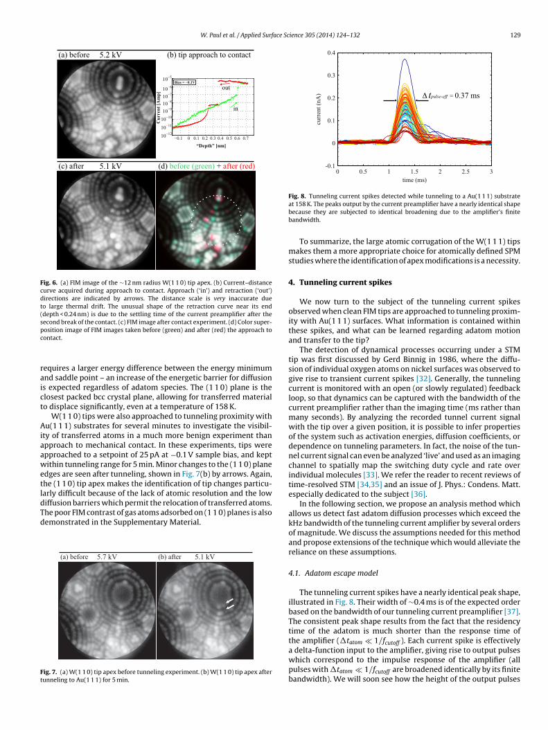
W. Paul et al. / Applied Surface Science 305 (2014) 124–132 129
5.2 kV(a) before (b) tip approach to contact
Cur
rent
[Am
p]
−0.1 0 0.1 0.2 0.3 0.4 0.5 0.6 0.710−1210−1110−10
10−8
10−9
10−710−6
10−5
“Depth” [nm]
Bias = −0.1V
in
out
5.1 kV(c) after (d) before (green) + after (red)
Fig. 6. (a) FIM image of the ∼12 nm radius W(1 1 0) tip apex. (b) Current–distancecurve acquired during approach to contact. Approach (‘in’) and retraction (‘out’)directions are indicated by arrows. The distance scale is very inaccurate dueto large thermal drift. The unusual shape of the retraction curve near its end(depth < 0.24 nm) is due to the settling time of the current preamplifier after thesecond break of the contact. (c) FIM image after contact experiment. (d) Color super-pc
raict
AiaawetldTd
Ft
0 0.5 1 1.5 2 2.5 3-0.1
0
0.1
0.2
0.3
0.4
time (ms)
curr
ent (
nA) tpulse-eff = 0.37 msΔ
Fig. 8. Tunneling current spikes detected while tunneling to a Au(1 1 1) substrate
osition image of FIM images taken before (green) and after (red) the approach toontact.
equires a larger energy difference between the energy minimumnd saddle point – an increase of the energetic barrier for diffusions expected regardless of adatom species. The (1 1 0) plane is thelosest packed bcc crystal plane, allowing for transferred materialo displace significantly, even at a temperature of 158 K.
W(1 1 0) tips were also approached to tunneling proximity withu(1 1 1) substrates for several minutes to investigate the visibil-
ty of transferred atoms in a much more benign experiment thanpproach to mechanical contact. In these experiments, tips werepproached to a setpoint of 25 pA at −0.1 V sample bias, and keptithin tunneling range for 5 min. Minor changes to the (1 1 0) plane
dges are seen after tunneling, shown in Fig. 7(b) by arrows. Again,he (1 1 0) tip apex makes the identification of tip changes particu-arly difficult because of the lack of atomic resolution and the lowiffusion barriers which permit the relocation of transferred atoms.
he poor FIM contrast of gas atoms adsorbed on (1 1 0) planes is alsoemonstrated in the Supplementary Material.5.7 kV(a) before 5.1 kV(b) after
ig. 7. (a) W(1 1 0) tip apex before tunneling experiment. (b) W(1 1 0) tip apex afterunneling to Au(1 1 1) for 5 min.
at 158 K. The peaks output by the current preamplifier have a nearly identical shapebecause they are subjected to identical broadening due to the amplifier’s finitebandwidth.
To summarize, the large atomic corrugation of the W(1 1 1) tipsmakes them a more appropriate choice for atomically defined SPMstudies where the identification of apex modifications is a necessity.
4. Tunneling current spikes
We now turn to the subject of the tunneling current spikesobserved when clean FIM tips are approached to tunneling proxim-ity with Au(1 1 1) surfaces. What information is contained withinthese spikes, and what can be learned regarding adatom motionand transfer to the tip?
The detection of dynamical processes occurring under a STMtip was first discussed by Gerd Binnig in 1986, where the diffu-sion of individual oxygen atoms on nickel surfaces was observed togive rise to transient current spikes [32]. Generally, the tunnelingcurrent is monitored with an open (or slowly regulated) feedbackloop, so that dynamics can be captured with the bandwidth of thecurrent preamplifier rather than the imaging time (ms rather thanmany seconds). By analyzing the recorded tunnel current signalwith the tip over a given position, it is possible to infer propertiesof the system such as activation energies, diffusion coefficients, ordependence on tunneling parameters. In fact, the noise of the tun-nel current signal can even be analyzed ‘live’ and used as an imagingchannel to spatially map the switching duty cycle and rate overindividual molecules [33]. We refer the reader to recent reviews oftime-resolved STM [34,35] and an issue of J. Phys.: Condens. Matt.especially dedicated to the subject [36].
In the following section, we propose an analysis method whichallows us detect fast adatom diffusion processes which exceed thekHz bandwidth of the tunneling current amplifier by several ordersof magnitude. We discuss the assumptions needed for this methodand propose extensions of the technique which would alleviate thereliance on these assumptions.
4.1. Adatom escape model
The tunneling current spikes have a nearly identical peak shape,illustrated in Fig. 8. Their width of ∼0.4 ms is of the expected orderbased on the bandwidth of our tunneling current preamplifier [37].The consistent peak shape results from the fact that the residencytime of the adatom is much shorter than the response time ofthe amplifier (�tatom � 1/fcutoff ). Each current spike is effectively
a delta-function input to the amplifier, giving rise to output pulseswhich correspond to the impulse response of the amplifier (allpulses with �tatom � 1/fcutoff are broadened identically by its finitebandwidth). We will soon see how the height of the output pulses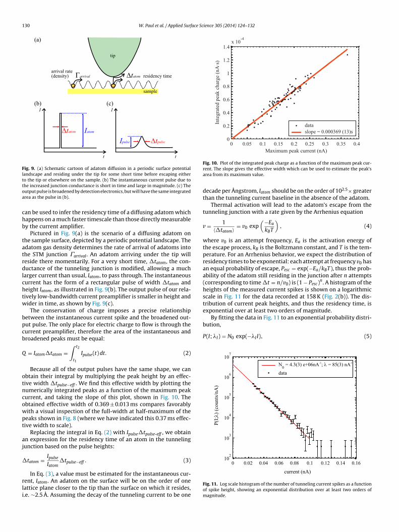
130 W. Paul et al. / Applied Surface Science 305 (2014) 124–132
tatomarrival residency tim e
tip
sample
(a)
tpulseIpulse
(b) (c)
tatom Iatom
I
t
I
t
arrival rate(density)
Fig. 9. (a) Schematic cartoon of adatom diffusion in a periodic surface potentiallandscape and residing under the tip for some short time before escaping eitherto the tip or elsewhere on the sample. (b) The instantaneous current pulse due totoa
chb
tatrdlchtw
bpcb
Q
otncowpt
aj
�
rli
0 0.05 0.1 0.15 0.2 0.25 0.3 0.35 0.40
0.2
0.4
0.6
0.8
1
1.2
1.4x 10
-4
Maximum peak current (nA)
Inte
grat
ed p
eak
char
ge (n
A·s)
dataslope = 0.000369 (13)s
By fitting the data in Fig. 11 to an exponential probability distri-bution,
P(I; �I) = N0 exp(−�II), (5)
0 0.02 0.04 0.06 0.08 0.1 0.12 0.14 0.1610
2
103
104
105
106
107
P(I;
)(co
unts
/nA
)
= 85(3) nA; = 4.3(3) e+06nAN 0
-1-1
data
he increased junction conductance is short in time and large in magnitude. (c) Theutput pulse is broadened by detection electronics, but will have the same integratedrea as the pulse in (b).
an be used to infer the residency time of a diffusing adatom whichappens on a much faster timescale than those directly measurabley the current amplifier.
Pictured in Fig. 9(a) is the scenario of a diffusing adatom onhe sample surface, depicted by a periodic potential landscape. Thedatom gas density determines the rate of arrival of adatoms intohe STM junction �arrival . An adatom arriving under the tip willeside there momentarily. For a very short time, �tatom, the con-uctance of the tunneling junction is modified, allowing a much
arger current than usual, Iatom, to pass through. The instantaneousurrent has the form of a rectangular pulse of width �tatom andeight Iatom, as illustrated in Fig. 9(b). The output pulse of our rela-ively low-bandwidth current preamplifier is smaller in height andider in time, as shown by Fig. 9(c).
The conservation of charge imposes a precise relationshipetween the instantaneous current spike and the broadened out-ut pulse. The only place for electric charge to flow is through theurrent preamplifier, therefore the area of the instantaneous androadened peaks must be equal:
= Iatom�tatom =∫ t2
t1
Ipulse(t) dt. (2)
Because all of the output pulses have the same shape, we canbtain their integral by multiplying the peak height by an effec-ive width �tpulse−eff . We find this effective width by plotting theumerically integrated peaks as a function of the maximum peakurrent, and taking the slope of this plot, shown in Fig. 10. Thebtained effective width of 0.369 ± 0.013 ms compares favorablyith a visual inspection of the full-width at half-maximum of theeaks shown in Fig. 8 (where we have indicated this 0.37 ms effec-ive width to scale).
Replacing the integral in Eq. (2) with Ipulse�tpulse-eff , we obtainn expression for the residency time of an atom in the tunnelingunction based on the pulse heights:
tatom = Ipulse
Iatom�tpulse−eff . (3)
In Eq. (3), a value must be estimated for the instantaneous cur-ent, Iatom. An adatom on the surface will be on the order of oneattice plane closer to the tip than the surface on which it resides,.e. ∼2.5 A. Assuming the decay of the tunneling current to be one
Fig. 10. Plot of the integrated peak charge as a function of the maximum peak cur-rent. The slope gives the effective width which can be used to estimate the peak’sarea from its maximum value.
decade per Ångstrom, Iatom should be on the order of 102.5× greaterthan the tunneling current baseline in the absence of the adatom.
Thermal activation will lead to the adatom’s escape from thetunneling junction with a rate given by the Arrhenius equation
v = 1〈�tatom〉 = v0 exp
(−Ea
kBT
), (4)
where v0 is an attempt frequency, Ea is the activation energy ofthe escape process, kB is the Boltzmann constant, and T is the tem-perature. For an Arrhenius behavior, we expect the distribution ofresidency times to be exponential: each attempt at frequency v0 hasan equal probability of escape, Pesc = exp(−Ea/kBT), thus the prob-ability of the adatom still residing in the junction after n attempts(corresponding to time �t = n/v0) is (1 − Pesc)n. A histogram of theheights of the measured current spikes is shown on a logarithmicscale in Fig. 11 for the data recorded at 158 K (Fig. 2(b)). The dis-tribution of current peak heights, and thus the residency time, isexponential over at least two orders of magnitude.
current (nA)
Fig. 11. Log scale histogram of the number of tunneling current spikes as a functionof spike height, showing an exponential distribution over at least two orders ofmagnitude.

ace Science 305 (2014) 124–132 131
aT0
p
E
v
rdstwttdE
N
t2rt
ey0oat
4
oa0t2TumiahlMwi
icTtaswqe(
-0.5 0 0.5 1 1.5 2-0.05
0
0.05
0.1
0.15
0.2
time (ms)
curr
ent (
nA)
W. Paul et al. / Applied Surf
mean pulse current of 〈Ipulse〉 = �−1I = 11.8 ± 0.4 pA is obtained.
his corresponds to a mean residency time of 〈�tatom〉 = 2.3 ±.1 �s.
Rearranging Eqs. (3) and (4), the activation energy for the escaperocess is given by:
a = kBT ln(v0〈�tatom〉) = kBT ln
(v0
�tpulse-eff
Iatom〈Ipulse〉
). (6)
Assuming an attempt frequency of 1012 to 1013 Hz [30], an acti-ation energy in the range of 0.20–0.23 eV is determined.
Finally, we consider whether any information about the arrivalate of adatoms, �arrival , can be obtained from the tunneling currentata. Given that the mean pulse current is about 10 pA, many of thepikes will pass below our detection threshold – simply measuringhe time between the pulses detected above a threshold of ∼25 pAill greatly overestimate the mean time between events. However,
he total number of events in the exponential probability distribu-ion of current pulses can be obtained by the fit parameters of theistribution (obtained by normalizing and analytically integratingq. (5)):
tot = N0
�. (7)
The rate of the current spikes can be calculated by dividing thisotal number by the acquisition time interval. A rate of � = 300 ±0 Hz is obtained for the data in Fig. 2(b) (though we believe theseates are artificially induced by tip-sample vibrations, discussed inhe next section).
Performing a similar analysis on the room-temperature data,xamination of the tunneling current spikes presented in Fig. 2(a)ields a mean pulse current of 3.6 ± 0.2 pA, corresponding to a.70 ± 0.04 �s residency time below the tip. The activation energyf the escape process is estimated to be 0.35–0.40 eV assuming anttempt frequency of 1012 to 1013 Hz. The mean pulse rate is foundo be 1040 ± 300 Hz.
.2. Discussion
From the exponential distributions of tunneling current spikesbtained in several experiments at 158 K and 298 K, we obtainctivation energies of Ea158 K = 0.19 ± 0.01 eV and Ea298 K = 0.360 ±.014 eV. The uncertainties quoted represent the standard devia-ion of the six measurements at 158 K and four measurements at98 K. Here, we have taken the attempt frequency to be 1012 Hz.he measurement of two different activation barriers is somewhatnexpected for the similar experimental configurations – theseay originate from two different escape mechanisms with differ-
ng energetics (for example, one for diffusion to another lattice site,nd one for transfer to the tip). A process requiring 0.36 eV willave a ∼3 × 10⁵ smaller rate at 158 K than at room temperature,
eading to very small statistics compared to the 0.19 eV process.eanwhile, the detection of a 0.19 eV process at room temperatureould require the measurement of ∼0.1 pA current spikes, which
s well below our current detection noise limit.Order-of-magnitude variations in our assumptions for the
nstantaneous peak current, Iatom, and the attempt frequency, v0,ontribute to errors in determined activation energies of kBT ln(10).his translates to 0.03 eV at 158 K, and 0.06 eV at room tempera-ure. If temperature could be varied slightly in these experiments,n Arrhenius analysis could be carried out by plotting the mea-ured mean residency time as a function of 1/Temperature. Not only
ould this alleviate the required assumption of the attempt fre-uency, but it would also make the obtained Ea independent of thestimation of the instantaneous tunneling current value, Iatom (Eq.3)). If the mean time were wrong by some factor because of the
Fig. 12. Time trace of the current for all spikes >50 pA showing a regular timeinterval between many of the sequential spikes.
instantaneous current estimation, it would appear at the interceptof the Arrhenius analysis, not in the slope:
ln(
1〈�tatom〉
)= ln(v0) + ln
(1˛
)− Ea
(1
kBT
). (8)
The mechanism causing the tunneling current spikes has notbeen determined here – it is assumed that the energy barriers wemeasure are for the adatom to escape from the tunneling junction,which could happen by diffusion to other lattice sites on the surface,or by transfer to the tip. Certainly, the presence of spikes in thetunneling current is correlated with tip changes in FIM, as discussedearlier and in Ref. [11]. Spikes in the tunneling current could alsoresult from rearrangements or adatoms diffusing on the tip itself.Comparison of the expected rate of adatom arrival (based on anestimated adatom gas density) to the measured rate of spikes mayhelp discern the source of these events, and may help to illuminatethe source of noise spikes in STM imaging.
It turns out that the arrival rate of adatoms deduced earlierfrom the integration of the exponential curves (Eq. (7)) does notrepresent the true value for the unperturbed surface because ofthe influence of the STM tip. It is apparent that in several of ourmeasurements, the tunneling current spikes are correlated in time.Fig. 12 shows a plot of all detected peaks above 50 pA in the data col-lected at 158 K, centered together at time 0 ms. A periodic trend isimmediately seen by eye – spikes are often followed by other spikesat regular time intervals of ∼0.75 ms. The reason for this could bea very small mechanical noise which serves to modulate the tip-sample separation very slightly, resulting in a regular tilting of theadatom energy landscape. Measurements of tip-sample vibrations(by monitoring the tunneling current in the lack of distance feed-back on stable Si(1 1 1)-2 × 1 and Cu(1 0 0) surfaces) suggest thatthe tip-sample gap stability is better than 20 pm. In atomistic sim-ulations, changes in tip-sample-separation of ∼30 pm have beenshown to decrease barriers for diffusion or atom transfer by up to∼0.2 eV [38]. Although the arrival of spikes is correlated in time,we expect that the escape process should be unaffected by thiscorrelation due to its relatively instantaneous timescale.
The extraction of the energy barrier for intrinsic adatom diffu-sion and the density of the adatom gas requires a non-interactingtip. From the direct observation of material transfer in FIM, weknow that there must be a reasonable force exerted by the tip onadatoms which lowers the energetic barrier for transfer sufficientlythat a finite number are transferred to the tip during measure-ments. Experiments performed at several tip-sample distances andapplied voltages should clarify the role of the tip in the statisticsof tunneling current spikes. For the moment, we have focused on
reasonable low-current tunneling conditions with the main goal ofassessing FIM tip integrity in STM experiments.Modifications of the adatom potential landscape due to thepresence of the tip are expected in two ways: The strong electric

1 ace Sc
fidtbdta
itbnsiri
5
fatibtpeotFits
w1aaredttoea
wttiteaa
[[[
[
[
[
[[[[
[[[[[[[[[[
[[
[[
[[[
32 W. Paul et al. / Applied Surf
eld in the tip-sample junction will interact with the adsorbateipole moment, leading to a broad potential well superposed onhe atomic corrugation [39,40]. In addition, the height of the energyarriers between binding sites on the surface are expected toecrease with the proximity of the tip [38]. We also refer the readero a discussion of possible atom transfer mechanisms by thermalctivation, tunneling, and field desorption by Gomer [41].
In a more sophisticated model of adatoms momentarily resid-ng in the STM junction, one may have to consider effects due tohe resolution of the tip – an instantaneously high current mighte measured while the adatom visits several sites under the tip,ot just one. The known geometry of our FIM tips provides a goodtarting point for such estimation. If one were interested in extract-ng the adatom gas density, one would also have to consider theeturn of the same adatom into the junction due to long-range tipnteractions.
. Summary and conclusion
To summarize, we have shown that the transfer of atoms occursrom Au(1 1 1) substrates to W tips. Transferred material diffuses to
great extent on W(1 1 1) tips at room temperature, but is confinedo the (1 1 1) apex when cooled to 158 K. W(1 1 0) tips were broughtnto mechanical contact with Au(1 1 1) at 158 K, and it proved toe more difficult to identify adsorbed atoms on these tips due tohe larger extent of diffusion on the (1 1 0) plane. Large, flat (1 1 0)lanes also hinder the characterization of the tip’s atomic geom-try due to the lack of atomic resolution and the poor resolutionf adsorbed material within the planes and at their edges. W(1 1 1)ips provide both high diffusion barriers and atomic resolution inIM, making them most appropriate for SPM studies with atom-cally defined tips. The transfer of atoms from Au(1 1 1) sampleso W tips cannot be eliminated at temperatures accessible to ourystem.
An exponential distribution of tunneling current peak heightsas observed when tunneling to Au(1 1 1) substrates at 298 K and
58 K. The mean peak heights were related to the residency time ofn adatom in the STM junction through the conservation of chargend an estimation of the instantaneous tunnel current. From theesidency time, the activation energy for adatom escape can bestimated. We have shown that even if not all events are above theetection noise, one can in principle integrate the exponential dis-ribution and infer the mean rate of spikes. The influence of the STMip, the detailed mechanisms of adatom escape, and the refinementf approximations remain open questions for future work in bothxperiments and atomistic modeling using the FIM tip structure as
well-defined starting point.We conclude from this work that the tip apex orientation
hich defines the relevant activation barriers for diffusion, andhe temperature at which experiments are carried out is of cen-ral importance to achieving a truly atomically defined experimentn SPM. In the absence of the time-of-flight characterization of
he transferred material to the tip, careful examination of fieldvaporation sequence provides evidence of tip changes throughdsorbate-promoted field evaporation. Finally, W(1 1 1) tip apicesre far better suited to atomically-defined SPM experiments due to[[[[[
ience 305 (2014) 124–132
their enhanced resolution in FIM and their larger diffusion barrierscompared to W(1 1 0) tips.
Acknowledgments
Funding from NSERC, CIFAR, and RQMP is gratefullyacknowledged.
Appendix A. Supplementary data
Supplementary data associated with this article can befound, in the online version, at http://dx.doi.org/10.1016/j.apsusc.2014.03.002.
References
[1] H.-W. Fink, IBM J. Res. Dev. 30 (1986) 460.[2] M. Ternes, C. González, C.P. Lutz, P. Hapala, F.J. Giessibl, P. Jelíinek, A.J. Heinrich,
Phys. Rev. Lett. 106 (2011) 016802.[3] W. Paul, D. Oliver, Y. Miyahara, P.H. Grütter, Phys. Rev. Lett. 110 (2013) 135506.[4] D.J. Oliver, J. Maassen, M. El Ouali, W. Paul, T. Hagedorn, Y. Miyahara, Y. Qi, H.
Guo, P.H. Grütter, Proc. Natl. Acad. Sci. U. S. A. 109 (2012) 19097.[5] F.J. Giessibl, Appl. Phys. Lett. 73 (1998) 3956.[6] S. Heike, T. Hashizume, Appl. Phys. Lett. 83 (2003) 3620.[7] T. An, T. Eguchi, K. Akiyama, Y. Hasegawa, Appl. Phys. Lett. 87 (2005) 133114.[8] J. Falter, G. Langewisch, H. Hölscher, H. Fuchs, a. Schirmeisen, Phys. Rev. B 87
(2013) 115412.[9] H. Mehrez, A. Wlasenko, B. Larade, J. Taylor, P. Grütter, H. Guo, Phys. Rev. B 65
(2002) 195419.10] Y. Xue, M. Ratner, Phys. Rev. B 68 (2003) 115407.11] W. Paul, Y. Miyahara, P.H. Grütter, Nanotechnology 23 (2012) 335702.12] M. Tomitori, N. Hirano, F. Iwawaki, Y. Watanabe, T. Takayanagi, O. Nishikawa,
J. Vac. Sci. Technol. A Vacuum, Surfaces, Film 8 (1990) 425.13] T. Hagedorn, M. El Ouali, W. Paul, D. Oliver, Y. Miyahara, P.H. Grütter, Rev. Sci.
Instrum. 82 (2011) 113903.14] A.-S. Lucier, Preparation and Characterization of Tungsten Tips Suitable for
Molecular Electronics Studies, McGill University, 2004.15] B. Verlinden, J. Driver, I. Samajdar, R.D. Doherty, Thermo-Mechanical Processing
of Metallic Materials, Elsevier, Oxford, 2007.16] M. Greiner, P. Kruse, Rev. Sci. Instrum. 78 (2007) 026104.17] W. Paul, P. Grütter, arXiv:1304.6766.18] A.-S. Lucier, H. Mortensen, Y. Sun, P.H. Grütter, Phys. Rev. B 72 (2005) 235420.19] T.T. Tsong, Atom-Probe Field Ion Microscopy, Cambridge University Press, New
York, 1990.20] G. Ehrlich, F.G. Hudda, J. Chem. Phys. 36 (1962) 3233.21] J.F. Mulson, E.W. Müller, J. Chem. Phys. 38 (1963) 2615.22] A.A. Holscher, W.M.H. Sachtler, Discuss. Faraday Soc. 41 (1966) 29.23] E.W. Müller, J.A. Panitz, S.B. McLane, Rev. Sci. Instrum. 39 (1968) 83.24] R.T. Lewis, R. Gomer, Surf. Sci. 26 (1971) 197.25] R.G. Forbes, Appl. Surf. Sci. 87–88 (1995) 1.26] K.J. Fraser, J.J. Boland, J. Sensors 2012 (2012) 961239.27] D.S. Whitmell, Surf. Sci. 11 (1968) 37.28] E.W. Müller, T.T. Tsong, Prog. Surf. Sci. 4 (1974) 1.29] G. Antczak, G. Ehrlich, Surface Diffusion, Cambridge University Press, New York,
2010.30] G.L. Kellogg, Surf. Sci. Rep. 21 (1994) 1.31] C.J. Chen, Introduction to Scanning Tunneling Microscopy, 2nd ed., Oxford Uni-
versity Press, Oxford, 2008.32] G. Binnig, H. Fuchs, E. Stoll, Surf. Sci. Lett. 169 (1986) L295.33] J. Schaffert, M.C. Cottin, A. Sonntag, H. Karacuban, C. a Bobisch, N. Lorente, J.-P.
Gauyacq, R. Möller, Nat. Mater. 12 (2012) 1.34] A. van Houselt, H.J.W. Zandvliet, Rev. Mod. Phys. 82 (2010) 1593.35] Q. Liu, K.-D. Wang, X.-D. Xiao, Front. Phys. China 5 (2010) 357.36] H.J.W. Zandvliet, N. Lin, J. Phys. Condens. Matter 22 (2010) 260301.
37] U. Dürig, L. Novotny, B. Michel, A. Stalder, Rev. Sci. Instrum. 68 (1997) 3814.38] M. Sørensen, K. Jacobsen, H. Jónsson, Phys. Rev. Lett. 77 (1996) 5067.39] J. Stroscio, D.M. Eigler, Science 254 (1991) 1319.40] L.J. Whitman, J.A. Stroscio, R.A. Dragoset, R.J. Celotta, Science 251 (1991) 1206.41] R. Gomer, IBM J. Res. Dev. 30 (1986) 428.