Embed Size (px)
Citation preview
1
FIGURE 1. Two-Pole Low-Pass Filter Using UAF42.
NOTE: A UAF42 and two external resistors make a unity-gain, two-pole, 1.25dB rippleChebyshev low-pass filter. With the resistor values shown, cutoff frequency is 10kHz.
Although active filters are vital in modern electronics, theirdesign and verification can be tedious and time consuming.To aid in the design of active filters, Burr-Brown provides aseries of FilterPro™ computer-aided design programs. Us-ing the FILTER42 program and the UAF42 it is easy todesign and implement all kinds of active filters. The UAF42is a monolithic IC which contains the op amps, matchedresistors, and precision capacitors needed for a state-variablefilter pole-pair. A fourth, uncommitted precision op amp isalso included on the die.
Filters implemented with the UAF42 are time-continuous,free from the switching noise and aliasing problems ofswitched-capacitor filters. Other advantages of the state-variable topology include low sensitivity of filter parametersto external component values and simultaneous low-pass,high-pass, and band-pass outputs. Simple two-pole filterscan be made with a UAF42 and two external resistors—seeFigure 1.
The DOS-compatible program guides you through the de-sign process and automatically calculates component values.Low-pass, high-pass, band-pass, and band-reject (or notch)filters can be designed.
Active filters are designed to approximate an ideal filterresponse. For example, an ideal low-pass filter completely
eliminates signals above the cutoff frequency (in the stop-band), and perfectly passes signals below it (in the pass-band). In real filters, various trade-offs are made in anattempt to approximate the ideal. Some filter types areoptimized for gain flatness in the pass-band, some trade-offgain variation or ripple in the pass-band for a steeper rate ofattenuation between the pass-band and stop-band (in thetransition-band), still others trade-off both flatness and rateof roll-off in favor of pulse-response fidelity. FILTER42supports the three most commonly used all-pole filter types:Butterworth, Chebyshev, and Bessel. The less familiar In-verse Chebyshev is also supported. If a two-pole band-passor notch filter is selected, the program defaults to a resonant-circuit response.
Butterworth (maximally flat magnitude). This filter has theflattest possible pass-band magnitude response. Attenuationis –3dB at the design cutoff frequency. Attenuation beyondthe cutoff frequency is a moderately steep –20dB/decade/pole. The pulse response of the Butterworth filter has mod-erate overshoot and ringing.
Chebyshev (equal ripple magnitude). (Other transliterationsof the Russian Heby]ov are Tschebychev, Tschebyscheffor Tchevysheff). This filter response has steeper initial rateof attenuation beyond the cutoff frequency than Butterworth.
A1
R2 50kΩ
A2 A3
R4 50kΩ
UAF42
11
R1
50kΩ
RF1 15.8kΩ
RF2 15.8kΩ
C1
1000pF
C2
1000pF
13 8 7 14
2 VIN
R3 50kΩ
VO 1
FILTER DESIGN PROGRAM FORTHE UAF42 UNIVERSAL ACTIVE FILTER
By Johnnie Molina and R. Mark Stitt (602) 746-7592
APPLICATION BULLETIN®
Mailing Address: PO Box 11400 • Tucson, AZ 85734 • Street Address: 6730 S. Tucson Blvd. • Tucson, AZ 85706Tel: (602) 746-1111 • Twx: 910-952-111 • Telex: 066-6491 • FAX (602) 889-1510 • Immediate Product Info: (800) 548-6132
©1991 Burr-Brown Corporation AB-035C Printed in U.S.A. July, 1993
SBFA002
2
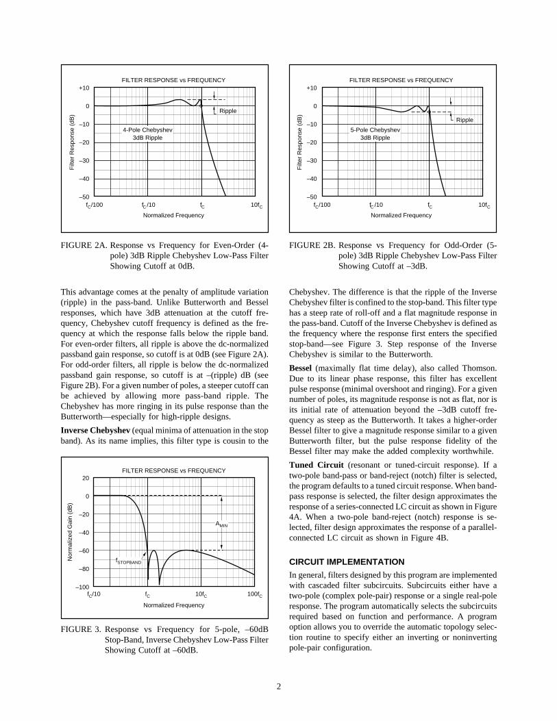
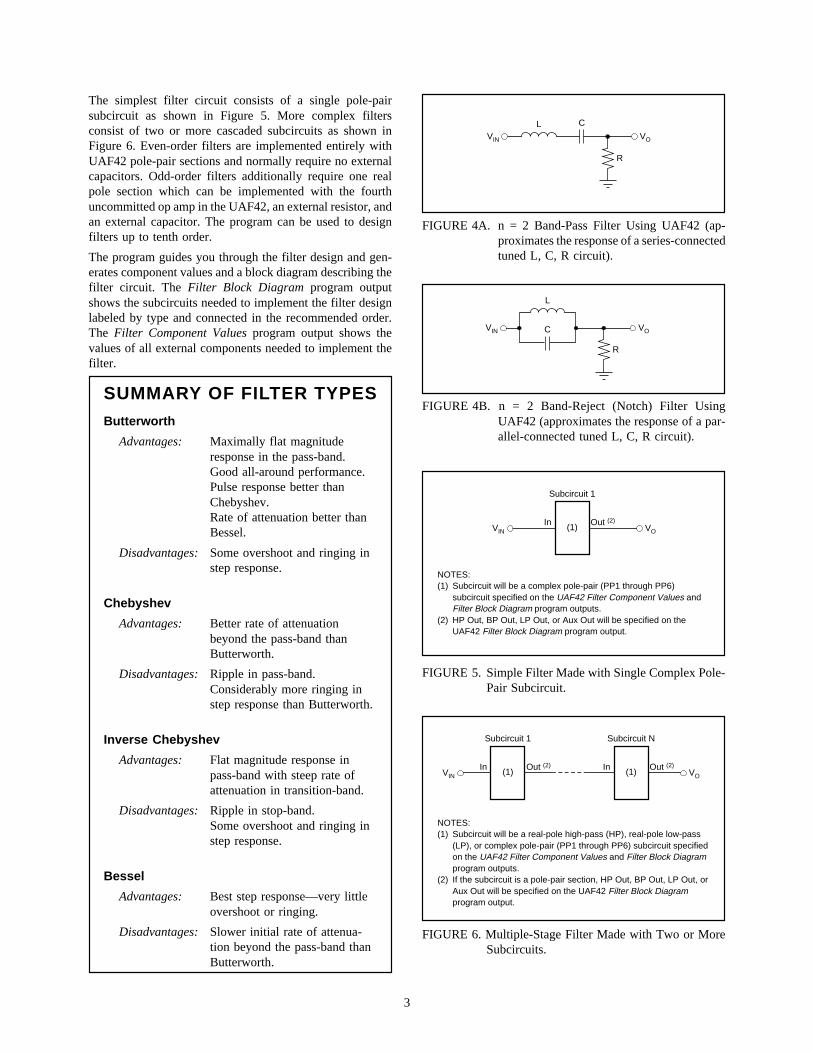
This advantage comes at the penalty of amplitude variation(ripple) in the pass-band. Unlike Butterworth and Besselresponses, which have 3dB attenuation at the cutoff fre-quency, Chebyshev cutoff frequency is defined as the fre-quency at which the response falls below the ripple band.For even-order filters, all ripple is above the dc-normalizedpassband gain response, so cutoff is at 0dB (see Figure 2A).For odd-order filters, all ripple is below the dc-normalizedpassband gain response, so cutoff is at –(ripple) dB (seeFigure 2B). For a given number of poles, a steeper cutoff canbe achieved by allowing more pass-band ripple. TheChebyshev has more ringing in its pulse response than theButterworth—especially for high-ripple designs.
Inverse Chebyshev (equal minima of attenuation in the stopband). As its name implies, this filter type is cousin to the
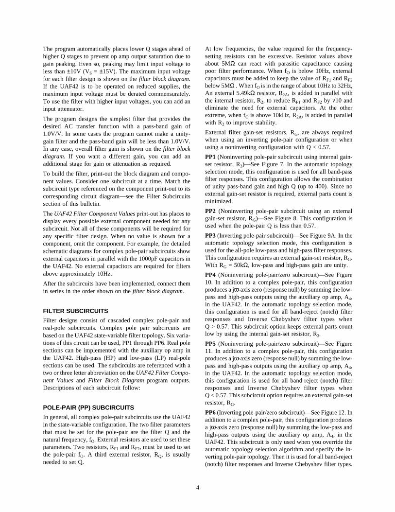
Chebyshev. The difference is that the ripple of the InverseChebyshev filter is confined to the stop-band. This filter typehas a steep rate of roll-off and a flat magnitude response inthe pass-band. Cutoff of the Inverse Chebyshev is defined asthe frequency where the response first enters the specifiedstop-band—see Figure 3. Step response of the InverseChebyshev is similar to the Butterworth.
Bessel (maximally flat time delay), also called Thomson.Due to its linear phase response, this filter has excellentpulse response (minimal overshoot and ringing). For a givennumber of poles, its magnitude response is not as flat, nor isits initial rate of attenuation beyond the –3dB cutoff fre-quency as steep as the Butterworth. It takes a higher-orderBessel filter to give a magnitude response similar to a givenButterworth filter, but the pulse response fidelity of theBessel filter may make the added complexity worthwhile.
Tuned Circuit (resonant or tuned-circuit response). If atwo-pole band-pass or band-reject (notch) filter is selected,the program defaults to a tuned circuit response. When band-pass response is selected, the filter design approximates theresponse of a series-connected LC circuit as shown in Figure4A. When a two-pole band-reject (notch) response is se-lected, filter design approximates the response of a parallel-connected LC circuit as shown in Figure 4B.
CIRCUIT IMPLEMENTATION
In general, filters designed by this program are implementedwith cascaded filter subcircuits. Subcircuits either have atwo-pole (complex pole-pair) response or a single real-poleresponse. The program automatically selects the subcircuitsrequired based on function and performance. A programoption allows you to override the automatic topology selec-tion routine to specify either an inverting or noninvertingpole-pair configuration.
FIGURE 3.Response vs Frequency for 5-pole, –60dBStop-Band, Inverse Chebyshev Low-Pass FilterShowing Cutoff at –60dB.
FILTER RESPONSE vs FREQUENCY
Normalized Frequency
f /100C f /10C f C 10f C
+10
0
–10
–20
–30
–40
–50
Filt
er R
espo
nse
(dB
)
5-Pole Chebyshev3dB Ripple
Ripple
FILTER RESPONSE vs FREQUENCY
Normalized Frequency
f /100C f /10C f C 10f C
+10
0
–10
–20
–30
–40
–50
Filt
er R
espo
nse
(dB
)
4-Pole Chebyshev3dB Ripple
Ripple
FIGURE 2A. Response vs Frequency for Even-Order (4-pole) 3dB Ripple Chebyshev Low-Pass FilterShowing Cutoff at 0dB.
FIGURE 2B. Response vs Frequency for Odd-Order (5-pole) 3dB Ripple Chebyshev Low-Pass FilterShowing Cutoff at –3dB.
FILTER RESPONSE vs FREQUENCY
fC/10
Normalized Frequency
fC 10fC 100fC
Nor
mal
ized
Gai
n (d
B)
20
0
–20
–40
–60
–80
–100
AMIN
fSTOPBAND
3
FIGURE 6. Multiple-Stage Filter Made with Two or MoreSubcircuits.
NOTES:(1) Subcircuit will be a real-pole high-pass (HP), real-pole low-pass
(LP), or complex pole-pair (PP1 through PP6) subcircuit specifiedon the UAF42 Filter Component Values and Filter Block Diagramprogram outputs.
(2) If the subcircuit is a pole-pair section, HP Out, BP Out, LP Out, orAux Out will be specified on the UAF42 Filter Block Diagramprogram output.
VIN VO
Subcircuit N
In Out(2) (1)
Subcircuit 1
In Out(2) (1)
NOTES:(1) Subcircuit will be a complex pole-pair (PP1 through PP6)
subcircuit specified on the UAF42 Filter Component Values andFilter Block Diagram program outputs.
(2) HP Out, BP Out, LP Out, or Aux Out will be specified on theUAF42 Filter Block Diagram program output.
VIN VO
Subcircuit 1
In Out(2) (1)
FIGURE 5. Simple Filter Made with Single Complex Pole-Pair Subcircuit.
FIGURE 4B. n = 2 Band-Reject (Notch) Filter UsingUAF42 (approximates the response of a par-allel-connected tuned L, C, R circuit).
FIGURE 4A. n = 2 Band-Pass Filter Using UAF42 (ap-proximates the response of a series-connectedtuned L, C, R circuit).
The simplest filter circuit consists of a single pole-pairsubcircuit as shown in Figure 5. More complex filtersconsist of two or more cascaded subcircuits as shown inFigure 6. Even-order filters are implemented entirely withUAF42 pole-pair sections and normally require no externalcapacitors. Odd-order filters additionally require one realpole section which can be implemented with the fourthuncommitted op amp in the UAF42, an external resistor, andan external capacitor. The program can be used to designfilters up to tenth order.
The program guides you through the filter design and gen-erates component values and a block diagram describing thefilter circuit. The Filter Block Diagram program outputshows the subcircuits needed to implement the filter designlabeled by type and connected in the recommended order.The Filter Component Values program output shows thevalues of all external components needed to implement thefilter.
C L VIN VO
R
C
L
VIN VO
R
SUMMARY OF FILTER TYPESButterworth
Advantages: Maximally flat magnituderesponse in the pass-band.Good all-around performance.Pulse response better thanChebyshev.Rate of attenuation better thanBessel.
Disadvantages: Some overshoot and ringing instep response.
Chebyshev
Advantages: Better rate of attenuationbeyond the pass-band thanButterworth.
Disadvantages: Ripple in pass-band.Considerably more ringing instep response than Butterworth.
Inverse Chebyshev
Advantages: Flat magnitude response inpass-band with steep rate ofattenuation in transition-band.
Disadvantages: Ripple in stop-band.Some overshoot and ringing instep response.
Bessel
Advantages: Best step response—very littleovershoot or ringing.
Disadvantages: Slower initial rate of attenua-tion beyond the pass-band thanButterworth.
4
At low frequencies, the value required for the frequency-setting resistors can be excessive. Resistor values aboveabout 5MΩ can react with parasitic capacitance causingpoor filter performance. When fO is below 10Hz, externalcapacitors must be added to keep the value of RF1 and RF2
below 5MΩ . When fO is in the range of about 10Hz to 32Hz,An external 5.49kΩ resistor, R2A, is added in parallel withthe internal resistor, R2, to reduce RF1 and RF2 by √10 andeliminate the need for external capacitors. At the otherextreme, when fO is above 10kHz, R2A, is added in parallelwith R2 to improve stability.
External filter gain-set resistors, RG, are always requiredwhen using an inverting pole-pair configuration or whenusing a noninverting configuration with Q < 0.57.
PP1 (Noninverting pole-pair subcircuit using internal gain-set resistor, R3)—See Figure 7. In the automatic topologyselection mode, this configuration is used for all band-passfilter responses. This configuration allows the combinationof unity pass-band gain and high Q (up to 400). Since noexternal gain-set resistor is required, external parts count isminimized.
PP2 (Noninverting pole-pair subcircuit using an externalgain-set resistor, RG)—See Figure 8. This configuration isused when the pole-pair Q is less than 0.57.
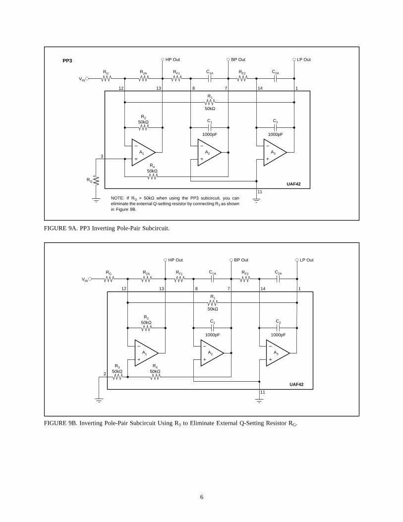
PP3 (Inverting pole-pair subcircuit)—See Figure 9A. In theautomatic topology selection mode, this configuration isused for the all-pole low-pass and high-pass filter responses.This configuration requires an external gain-set resistor, RG.With RG = 50kΩ, low-pass and high-pass gain are unity.
PP4 (Noninverting pole-pair/zero subcircuit)—See Figure10. In addition to a complex pole-pair, this configurationproduces a jω-axis zero (response null) by summing the low-pass and high-pass outputs using the auxiliary op amp, A4,in the UAF42. In the automatic topology selection mode,this configuration is used for all band-reject (notch) filterresponses and Inverse Chebyshev filter types whenQ > 0.57. This subcircuit option keeps external parts countlow by using the internal gain-set resistor, R3.
PP5 (Noninverting pole-pair/zero subcircuit)—See Figure11. In addition to a complex pole-pair, this configurationproduces a jω-axis zero (response null) by summing the low-pass and high-pass outputs using the auxiliary op amp, A4,in the UAF42. In the automatic topology selection mode,this configuration is used for all band-reject (notch) filterresponses and Inverse Chebyshev filter types whenQ < 0.57. This subcircuit option requires an external gain-setresistor, RG.
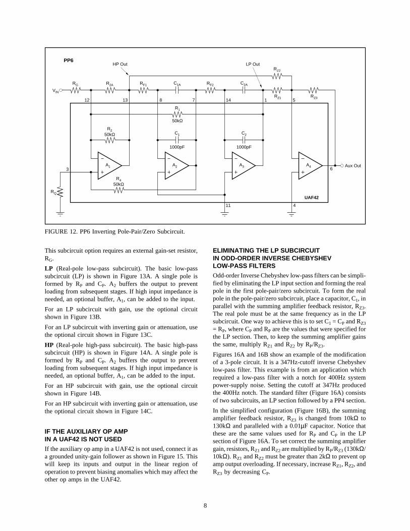
PP6 (Inverting pole-pair/zero subcircuit)—See Figure 12. Inaddition to a complex pole-pair, this configuration producesa jω-axis zero (response null) by summing the low-pass andhigh-pass outputs using the auxiliary op amp, A4, in theUAF42. This subcircuit is only used when you override theautomatic topology selection algorithm and specify the in-verting pole-pair topology. Then it is used for all band-reject(notch) filter responses and Inverse Chebyshev filter types.
The program automatically places lower Q stages ahead ofhigher Q stages to prevent op amp output saturation due togain peaking. Even so, peaking may limit input voltage toless than ±10V (VS = ±15V). The maximum input voltagefor each filter design is shown on the filter block diagram.If the UAF42 is to be operated on reduced supplies, themaximum input voltage must be derated commensurately.To use the filter with higher input voltages, you can add aninput attenuator.
The program designs the simplest filter that provides thedesired AC transfer function with a pass-band gain of1.0V/V. In some cases the program cannot make a unity-gain filter and the pass-band gain will be less than 1.0V/V.In any case, overall filter gain is shown on the filter blockdiagram. If you want a different gain, you can add anadditional stage for gain or attenuation as required.
To build the filter, print-out the block diagram and compo-nent values. Consider one subcircuit at a time. Match thesubcircuit type referenced on the component print-out to itscorresponding circuit diagram—see the Filter Subcircuitssection of this bulletin.
The UAF42 Filter Component Values print-out has places todisplay every possible external component needed for anysubcircuit. Not all of these components will be required forany specific filter design. When no value is shown for acomponent, omit the component. For example, the detailedschematic diagrams for complex pole-pair subcircuits showexternal capacitors in parallel with the 1000pF capacitors inthe UAF42. No external capacitors are required for filtersabove approximately 10Hz.
After the subcircuits have been implemented, connect themin series in the order shown on the filter block diagram.
FILTER SUBCIRCUITS
Filter designs consist of cascaded complex pole-pair andreal-pole subcircuits. Complex pole pair subcircuits arebased on the UAF42 state-variable filter topology. Six varia-tions of this circuit can be used, PP1 through PP6. Real polesections can be implemented with the auxiliary op amp inthe UAF42. High-pass (HP) and low-pass (LP) real-polesections can be used. The subcircuits are referenced with atwo or three letter abbreviation on the UAF42 Filter Compo-nent Values and Filter Block Diagram program outputs.Descriptions of each subcircuit follow:
POLE-PAIR (PP) SUBCIRCUITS
In general, all complex pole-pair subcircuits use the UAF42in the state-variable configuration. The two filter parametersthat must be set for the pole-pair are the filter Q and thenatural frequency, fO. External resistors are used to set theseparameters. Two resistors, RF1 and RF2, must be used to setthe pole-pair fO. A third external resistor, RQ, is usuallyneeded to set Q.
5
FIGURE 7. PP1 Noninverting Pole-Pair Subcircuit Using Internal Gain-Set Resistor R3.
FIGURE 8. PP2 Noninverting Pole-Pair Subcircuit Using External Gain-Set Resistor RG.
PP1
PP2
A1
R2 50kΩ
A2 A3
R3 50kΩ
R4 50kΩ
UAF42
11
R1
50kΩ
RF1 RF2
C1
1000pF
C2
1000pF
VIN2
13 8 7 14
3
RQ
R2A C1A
C2A
LP OutBP OutHP Out
112
A1
R2 50kΩ
A2 A3
R4 50kΩ
UAF42
11
R1
50kΩ
RF1 RF2
C1
1000pF
C2
1000pF
VIN3
13 8 7 14
RQ
R2A C1A
C2A
LP OutBP OutHP Out
112
RG
6
FIGURE 9A. PP3 Inverting Pole-Pair Subcircuit.
NOTE: If RQ = 50kΩ when using the PP3 subcircuit, you caneliminate the external Q-setting resistor by connecting R3 as shownin Figure 9B.
FIGURE 9B. Inverting Pole-Pair Subcircuit Using R3 to Eliminate External Q-Setting Resistor RG.
PP3
A1
R2 50kΩ
A2 A3
R4 50kΩ
UAF42
11
R1
50kΩ
RF1 RF2
C1
1000pF
C2
1000pF
3
13 8 7 14
RQ
R2A C1A
C2A
LP OutBP OutHP Out
112
RG
VIN
A1
R2 50kΩ
A2 A3
R4 50kΩ
UAF42
11
R1
50kΩ
RF1 RF2
C1
1000pF
C2
1000pF
2
13 8 7 14
R3 50kΩ
R2A C1A
C2A
LP OutBP OutHP Out
112
RG
VIN

7
FIGURE 10. PP4 Noninverting Pole-Pair/Zero Subcircuit Using Internal Gain-Set Resistor R3.
FIGURE 11. PP5 Noninverting Pole-Pair/Zero Subcircuit Using External Gain-Set Resistor RG.
PP5
PP4
A1
R2 50kΩ
A2 A3
R3 50kΩ
R4 50kΩ
UAF42
11
R1
50kΩ
RF1 RF2
C1
1000pF
C2
1000pF
VIN2
13 8 7 14
3
RQ
R2A C1A
C2A
HP Out
112
A4
4
RZ15
Aux Out
6
RZ2
RZ3
LP Out
A1
R2 50kΩ
A2 A3RG
R4 50kΩ
UAF42
11
R1
50kΩ
RF1 RF2
C1
1000pF
C2
1000pF
VIN3
13 8 7 14
RQ
R2A C1A
C2A
HP Out
112
A4
4
RZ15
Aux Out
6
RZ2
RZ3
LP Out
The information provided herein is believed to be reliable; however, BURR-BROWN assumes no responsibility for inaccuracies or omissions. BURR-BROWN assumesno responsibility for the use of this information, and all use of such information shall be entirely at the user’s own risk. Prices and specifications are subject to changewithout notice. No patent rights or licenses to any of the circuits described herein are implied or granted to any third party. BURR-BROWN does not authorize or warrantany BURR-BROWN product for use in life support devices and/or systems.
8
This subcircuit option requires an external gain-set resistor,RG.
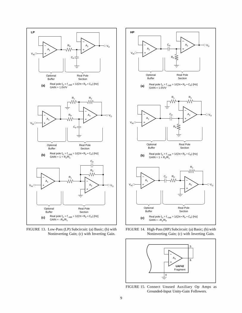
LP (Real-pole low-pass subcircuit). The basic low-passsubcircuit (LP) is shown in Figure 13A. A single pole isformed by RP and CP. A2 buffers the output to preventloading from subsequent stages. If high input impedance isneeded, an optional buffer, A1, can be added to the input.
For an LP subcircuit with gain, use the optional circuitshown in Figure 13B.
For an LP subcircuit with inverting gain or attenuation, usethe optional circuit shown in Figure 13C.
HP (Real-pole high-pass subcircuit). The basic high-passsubcircuit (HP) is shown in Figure 14A. A single pole isformed by RP and CP. A2 buffers the output to preventloading from subsequent stages. If high input impedance isneeded, an optional buffer, A1, can be added to the input.
For an HP subcircuit with gain, use the optional circuitshown in Figure 14B.
For an HP subcircuit with inverting gain or attenuation, usethe optional circuit shown in Figure 14C.
IF THE AUXILIARY OP AMPIN A UAF42 IS NOT USED
If the auxiliary op amp in a UAF42 is not used, connect it asa grounded unity-gain follower as shown in Figure 15. Thiswill keep its inputs and output in the linear region ofoperation to prevent biasing anomalies which may affect theother op amps in the UAF42.
FIGURE 12. PP6 Inverting Pole-Pair/Zero Subcircuit.
ELIMINATING THE LP SUBCIRCUITIN ODD-ORDER INVERSE CHEBYSHEVLOW-PASS FILTERS
Odd-order Inverse Chebyshev low-pass filters can be simpli-fied by eliminating the LP input section and forming the realpole in the first pole-pair/zero subcircuit. To form the realpole in the pole-pair/zero subcircuit, place a capacitor, C1, inparallel with the summing amplifier feedback resistor, RZ3.The real pole must be at the same frequency as in the LPsubcircuit. One way to achieve this is to set C1 = CP and RZ3
= RP, where CP and RP are the values that were specified forthe LP section. Then, to keep the summing amplifier gainsthe same, multiply RZ1 and RZ2 by RP/RZ3.
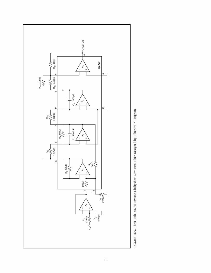
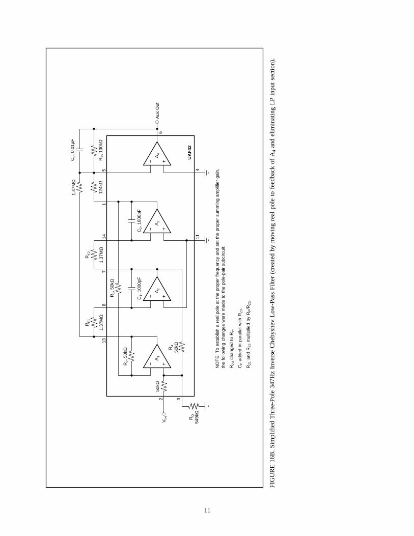
Figures 16A and 16B show an example of the modificationof a 3-pole circuit. It is a 347Hz-cutoff inverse Chebyshevlow-pass filter. This example is from an application whichrequired a low-pass filter with a notch for 400Hz systempower-supply noise. Setting the cutoff at 347Hz producedthe 400Hz notch. The standard filter (Figure 16A) consistsof two subcircuits, an LP section followed by a PP4 section.
In the simplified configuration (Figure 16B), the summingamplifier feedback resistor, RZ3 is changed from 10kΩ to130kΩ and paralleled with a 0.01µF capacitor. Notice thatthese are the same values used for RP and CP in the LPsection of Figure 16A. To set correct the summing amplifiergain, resistors, RZ1 and RZ2 are multiplied by RP/RZ3 (130kΩ/10kΩ). RZ1 and RZ2 must be greater than 2kΩ to prevent opamp output overloading. If necessary, increase RZ1, RZ2, andRZ3 by decreasing CP.
PP6
A1
R2 50kΩ
A2 A3
R4 50kΩ
UAF42
11
R1
50kΩ
RF1 RF2
C1
1000pF
C2
1000pF
3
13 8 7 14
RQ
R2A C1A
C2A
HP Out
112
A4
4
RZ15
Aux Out6
RZ2
RZ3
LP Out
RG
VIN
9
FIGURE 15. Connect Unused Auxiliary Op Amps asGrounded-Input Unity-Gain Followers.
FIGURE 13. Low-Pass (LP) Subcircuit: (a) Basic; (b) withNoninverting Gain; (c) with Inverting Gain.
FIGURE 14. High-Pass (HP) Subcircuit: (a) Basic; (b) withNoninverting Gain; (c) with Inverting Gain.
A2 VO
A1
VIN
Optional Buffer
Real Pole Section
RP
A2 VOA1
VIN
Optional Buffer
Real Pole Section
A2
CP
VOA1
VIN
Optional Buffer
Real Pole Section
R2R1
R1
CP
RP
CP
RP
(c)
(b)
(a) Real pole fO = f–3dB = 1/(2π • RP • CP) [Hz] GAIN = 1.0V/V
Real pole fO = f–3dB = 1/(2π • RP • CP) [Hz] GAIN = 1 + R2/R1
Real pole fO = f–3dB = 1/(2π • RP • CP) [Hz] GAIN = –RP/R1
(c)
A2 VO
CP
A1
VIN
Optional Buffer
Real Pole Section
R2
(b)
A2
RP
VOCP
A1
VIN
Optional Buffer
Real Pole Section
(a)
A2
RP
VOCP
A1
VIN
Optional Buffer
Real Pole Section
R2R1
RP
Real pole fO = f–3dB = 1/(2π • RP • CP) [Hz] GAIN = 1.0V/V
Real pole fO = f–3dB = 1/(2π • RP • CP) [Hz] GAIN = 1 + R2/R1
Real pole fO = f–3dB = 1/(2π • RP • CP) [Hz] GAIN = –R2/RP
UAF42 Fragment
A4
4
6
5
LP HP
10
A1
R2,
50k
Ω
A2
A3
50kΩ
R4
50kΩ
UA
F42
11
R1,
50k
Ω
RF
1
1.37
MΩ
RF
2
1.37
MΩ
C1,
100
0pF
2
138
714
3
1
A4
4
RZ
1, 9
.53k
Ω5
Aux
Out
6
RZ
2, 1
13kΩ
RZ
3, 1
0kΩ
RQ
549k
Ω
C2,
100
0pF
A5
RP
130k
ΩV
IN
CP
0.01
µF
FIG
UR
E 1
6A.
Thr
ee-P
ole
347H
z In
vers
e C
heby
shev
Low
-Pas
s F
ilter
Des
igne
d by
Filt
erP
ro™
Pro
gram
.
11
A1
R2,
50k
Ω
A2
A3
50kΩ
R4
50kΩ
UA
F42
11
R1,
50k
Ω
RF
1
1.37
MΩ
RF
2
1.37
MΩ
C1,
100
0pF
VIN
2
138
714
3
1
A4
4
124k
Ω5
Aux
Out
6
RP, 1
30kΩ
RQ
549k
Ω
1.47
MΩ
CP, 0
.01µ
F
C2,
100
0pF
NO
TE
: T
o es
tabl
ish
a re
al p
ole
at t
he p
rope
r fr
eque
ncy
and
set
the
prop
er s
umm
ing
ampl
ifier
gai
n,th
e fo
llow
ing
chan
ges
wer
e m
ade
to t
he p
ole-
pair
subc
ircui
t:
RZ
3 ch
ange
d to
RP.
CP a
dded
in
para
llel
with
RZ
3.
RZ
1 an
d R
Z2
mul
tiplie
d by
RP/R
Z3.
FIG
UR
E 1
6B.
Sim
plifi
ed T
hree
-Pol
e 34
7Hz
Inve
rse
Che
bysh
ev L
ow-P
ass
Filt
er (
crea
ted
by m
ovin
g re
al p
ole
to f
eedb
ack
of A
4 an
d el
imin
atin
g LP
inp
ut s
ectio
n).
12
Q ENHANCEMENT
When the fO • Q product required for a pole-pair section isabove ≈100kHz at frequencies above ≈3kHz, op amp gain-bandwidth limitations can cause Q errors and gain peaking.To mitigate this effect, the program automatically compen-sates for the expected error by decreasing the design-Qaccording to a Q-compensation algorithm(1). When thisoccurs, the value under the Q heading on the UAF42 FilterComponent Values print-out will be marked with an asteriskindicating that it is the theoretical Q, not the actual designQ. The actual design Q will be shown under an addedheading labeled QCOMP.
USING THE FilterPro™ PROGRAM
With each data entry, the program automatically calculatesfilter performance. This allows you to use a “what if”spreadsheet-type design approach. For example; you canquickly determine, by trial and error, how many poles areneeded for a desired roll-off.
GETTING STARTED
The first time you use the program, you may want to followthese suggested steps.
Type FILTER42 <ENTER> to start the program.
Use the arrow keys to move the cursor to the FilterResponse section.
1) SELECT FILTER RESPONSE
Press <ENTER> to toggle through four response choices:
Low-passHigh-passBand-passNotch (band-reject)
When the desired response appears, move the cursor to theFilter Type section.
2) SELECT FILTER TYPE
Move the cursor to the desired filter type and press<ENTER>. The selected filter type is highlighted and markedwith an asterisk. There are four filter-type choices:
Butterworth BesselChebyshev Inverse Chebyshev
If you choose Chebyshev, you must also enter ripple (i.e.pass-band ripple—see Chebyshev filter description).
If you choose Inverse Chebyshev, you must also enter AMIN
(i.e. min attenuation or max gain in stop-band—see InverseChebyshev filter description).
3) ENTER FILTER ORDER
Move the cursor to the Filter Order line in the Parameterssection. Enter filter order n (from 2 to 10).
4A) ENTER FILTER FREQUENCY
Move the cursor to the Filter Frequency line in the Param-eters section.
Low-pass/high-pass filter: enter the f–3dB or cutoff frequency.
Band-pass filter: enter the center frequency, fCENTER.
Band-reject (notch) filter: enter the notch frequency, fNOTCH.
If your filter is low-pass or high-pass, go to step 5.
4B) ENTER FILTER BANDWIDTH
If the filter is a band-pass or band-reject (notch), move thecursor to the bandwidth line and enter bandwidth.
If you press <ENTER> with no entry on the bandwidth line,you can enter fL and fH instead of bandwidth. fL and fH arethe f–3dB points with regard to the center frequency forButterworth and Bessel filters. They are the end of theripple-band for Chebyshev types. This method of entry mayforce a change in center frequency or notch frequency.
5) PRINT-OUT COMPONENT VALUES
Press function key <F4> to print-out Filter ComponentValues and a Filter Block Diagram . Follow the instructionsin the filter implementation section of this bulletin to as-semble a working filter.
USING THE PLOT FEATURE
A Plot feature allows you to view graphical results of filtergain and phase vs frequency. This feature is useful forcomparing filter types.
To view a plot of the current filter design, press <F2>.
GRAPHIC DISPLAY COMMANDS
While viewing the graphic display, several commands canbe used to compare filter responses:
<F1> or S—Saves the plot of the current design for futurerecall.
<F2> or R—Recalls the Saved plot and plots it along withthe current design.
<F3> or Z—Plots a Zero dB reference line.
GRAPHIC DISPLAY CURSOR CONTROL
While viewing the graphics display you can also use thearrow keys to move a cursor and view gain and phase forplotted filter responses.
RESISTOR VALUES
With each data entry, the program automatically calculatesresistor values. If external capacitors are needed, the pro-gram selects standard capacitor values and calculates exactresistor values for the filter you have selected. The 1%Resistors option in the Display menu can be used to calcu-late the closest standard 1% resistor values instead of exactresistor values. To use this feature, move the cursor to theresistors line in the Filter Response section and press
(1) L.P. Huelsman and P. E. Allen, Theory and Design of ActiveFilters, p. 241.
13
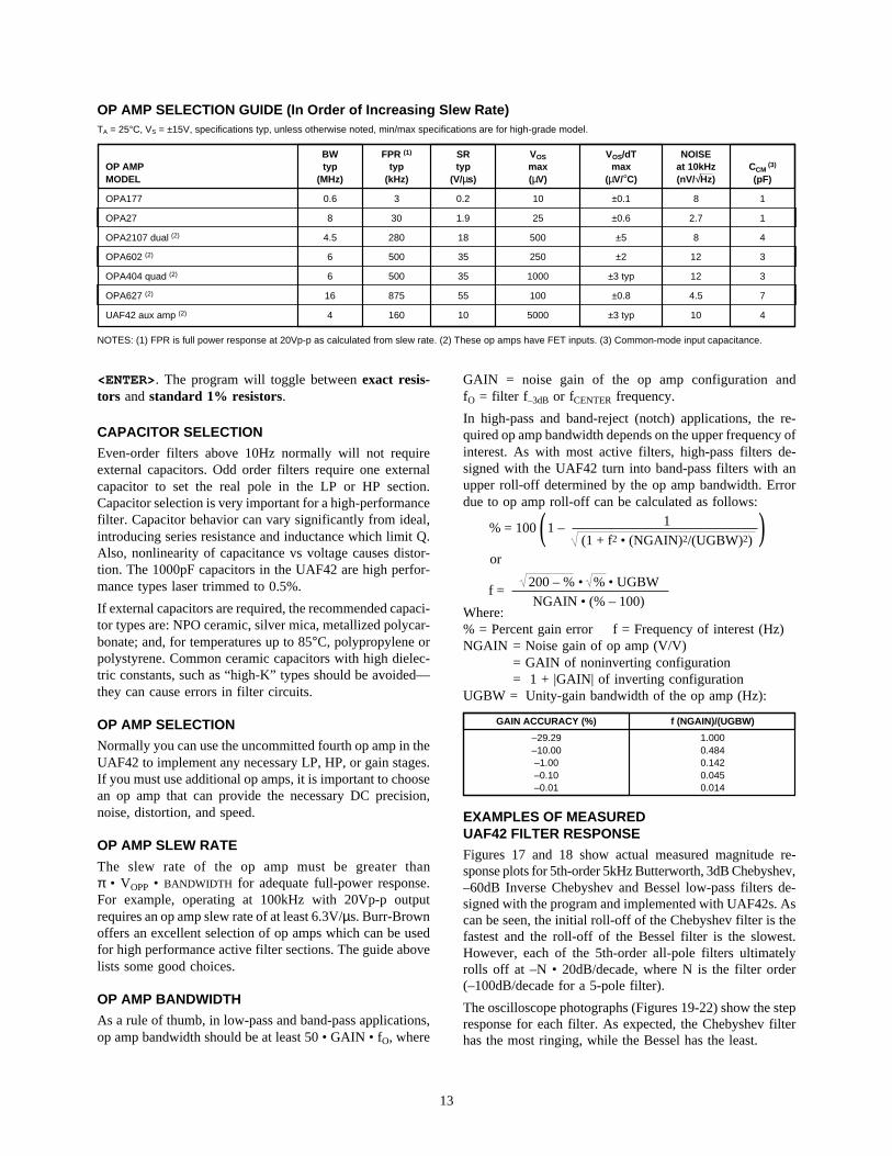
OP AMP SELECTION GUIDE (In Order of Increasing Slew Rate)TA = 25°C, VS = ±15V, specifications typ, unless otherwise noted, min/max specifications are for high-grade model.
BW FPR (1) SR VOS VOS/dT NOISEOP AMP typ typ typ max max at 10kHz C CM
(3)
MODEL (MHz) (kHz) (V/µs) (µV) (µV/°C) (nV/√Hz) (pF)
OPA177 0.6 3 0.2 10 ±0.1 8 1
OPA27 8 30 1.9 25 ±0.6 2.7 1
OPA2107 dual (2) 4.5 280 18 500 ±5 8 4
OPA602 (2) 6 500 35 250 ±2 12 3
OPA404 quad (2) 6 500 35 1000 ±3 typ 12 3
OPA627 (2) 16 875 55 100 ±0.8 4.5 7
UAF42 aux amp (2) 4 160 10 5000 ±3 typ 10 4
NOTES: (1) FPR is full power response at 20Vp-p as calculated from slew rate. (2) These op amps have FET inputs. (3) Common-mode input capacitance.
<ENTER>. The program will toggle between exact resis-tors and standard 1% resistors.
CAPACITOR SELECTION
Even-order filters above 10Hz normally will not requireexternal capacitors. Odd order filters require one externalcapacitor to set the real pole in the LP or HP section.Capacitor selection is very important for a high-performancefilter. Capacitor behavior can vary significantly from ideal,introducing series resistance and inductance which limit Q.Also, nonlinearity of capacitance vs voltage causes distor-tion. The 1000pF capacitors in the UAF42 are high perfor-mance types laser trimmed to 0.5%.
If external capacitors are required, the recommended capaci-tor types are: NPO ceramic, silver mica, metallized polycar-bonate; and, for temperatures up to 85°C, polypropylene orpolystyrene. Common ceramic capacitors with high dielec-tric constants, such as “high-K” types should be avoided—they can cause errors in filter circuits.
OP AMP SELECTION
Normally you can use the uncommitted fourth op amp in theUAF42 to implement any necessary LP, HP, or gain stages.If you must use additional op amps, it is important to choosean op amp that can provide the necessary DC precision,noise, distortion, and speed.
OP AMP SLEW RATE
The slew rate of the op amp must be greater thanπ • VOPP • BANDWIDTH for adequate full-power response.For example, operating at 100kHz with 20Vp-p outputrequires an op amp slew rate of at least 6.3V/µs. Burr-Brownoffers an excellent selection of op amps which can be usedfor high performance active filter sections. The guide abovelists some good choices.
OP AMP BANDWIDTH
As a rule of thumb, in low-pass and band-pass applications,op amp bandwidth should be at least 50 • GAIN • fO, where
GAIN = noise gain of the op amp configuration andfO = filter f–3dB or fCENTER frequency.
In high-pass and band-reject (notch) applications, the re-quired op amp bandwidth depends on the upper frequency ofinterest. As with most active filters, high-pass filters de-signed with the UAF42 turn into band-pass filters with anupper roll-off determined by the op amp bandwidth. Errordue to op amp roll-off can be calculated as follows:
% = 100 1 – 1
(1 + f2 • (NGAIN)2/(UGBW)2)( )or
f = 200 – % • % • UGBW
NGAIN • (% – 100)Where:% = Percent gain error f = Frequency of interest (Hz)NGAIN = Noise gain of op amp (V/V)
= GAIN of noninverting configuration= 1 + |GAIN| of inverting configuration
UGBW = Unity-gain bandwidth of the op amp (Hz):
GAIN ACCURACY (%) f (NGAIN)/(UGBW)
–29.29 1.000–10.00 0.484–1.00 0.142–0.10 0.045–0.01 0.014
EXAMPLES OF MEASUREDUAF42 FILTER RESPONSE
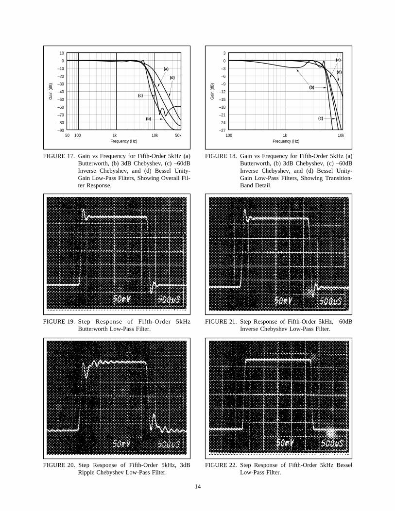
Figures 17 and 18 show actual measured magnitude re-sponse plots for 5th-order 5kHz Butterworth, 3dB Chebyshev,–60dB Inverse Chebyshev and Bessel low-pass filters de-signed with the program and implemented with UAF42s. Ascan be seen, the initial roll-off of the Chebyshev filter is thefastest and the roll-off of the Bessel filter is the slowest.However, each of the 5th-order all-pole filters ultimatelyrolls off at –N • 20dB/decade, where N is the filter order(–100dB/decade for a 5-pole filter).
The oscilloscope photographs (Figures 19-22) show the stepresponse for each filter. As expected, the Chebyshev filterhas the most ringing, while the Bessel has the least.
14
FIGURE 17. Gain vs Frequency for Fifth-Order 5kHz (a)Butterworth, (b) 3dB Chebyshev, (c) –60dBInverse Chebyshev, and (d) Bessel Unity-Gain Low-Pass Filters, Showing Overall Fil-ter Response.
Frequency (Hz) 50 100 1k 50k
Gai
n (d
B)
10
0
–10
–20
–30
–40
–50
–60
–70
–80
–90 10k
(a)
(d)
(b)
(c)
FIGURE 18. Gain vs Frequency for Fifth-Order 5kHz (a)Butterworth, (b) 3dB Chebyshev, (c) –60dBInverse Chebyshev, and (d) Bessel Unity-Gain Low-Pass Filters, Showing Transition-Band Detail.
Frequency (Hz) 100 1k 10k
Gai
n (d
B)
3
0
–3
–6
–9
–12
–15
–18
–21
–24
–27
(a)
(d)
(b)
(c)
FIGURE 19. Step Response of Fifth-Order 5kHzButterworth Low-Pass Filter.
FIGURE 21. Step Response of Fifth-Order 5kHz, –60dBInverse Chebyshev Low-Pass Filter.
FIGURE 20. Step Response of Fifth-Order 5kHz, 3dBRipple Chebyshev Low-Pass Filter.
FIGURE 22. Step Response of Fifth-Order 5kHz BesselLow-Pass Filter.
IMPORTANT NOTICE
Texas Instruments and its subsidiaries (TI) reserve the right to make changes to their products or to discontinueany product or service without notice, and advise customers to obtain the latest version of relevant informationto verify, before placing orders, that information being relied on is current and complete. All products are soldsubject to the terms and conditions of sale supplied at the time of order acknowledgment, including thosepertaining to warranty, patent infringement, and limitation of liability.
TI warrants performance of its semiconductor products to the specifications applicable at the time of sale inaccordance with TI’s standard warranty. Testing and other quality control techniques are utilized to the extentTI deems necessary to support this warranty. Specific testing of all parameters of each device is not necessarilyperformed, except those mandated by government requirements.
Customers are responsible for their applications using TI components.
In order to minimize risks associated with the customer’s applications, adequate design and operatingsafeguards must be provided by the customer to minimize inherent or procedural hazards.
TI assumes no liability for applications assistance or customer product design. TI does not warrant or representthat any license, either express or implied, is granted under any patent right, copyright, mask work right, or otherintellectual property right of TI covering or relating to any combination, machine, or process in which suchsemiconductor products or services might be or are used. TI’s publication of information regarding any thirdparty’s products or services does not constitute TI’s approval, warranty or endorsement thereof.
Copyright 2000, Texas Instruments Incorporated