Embed Size (px)
Citation preview
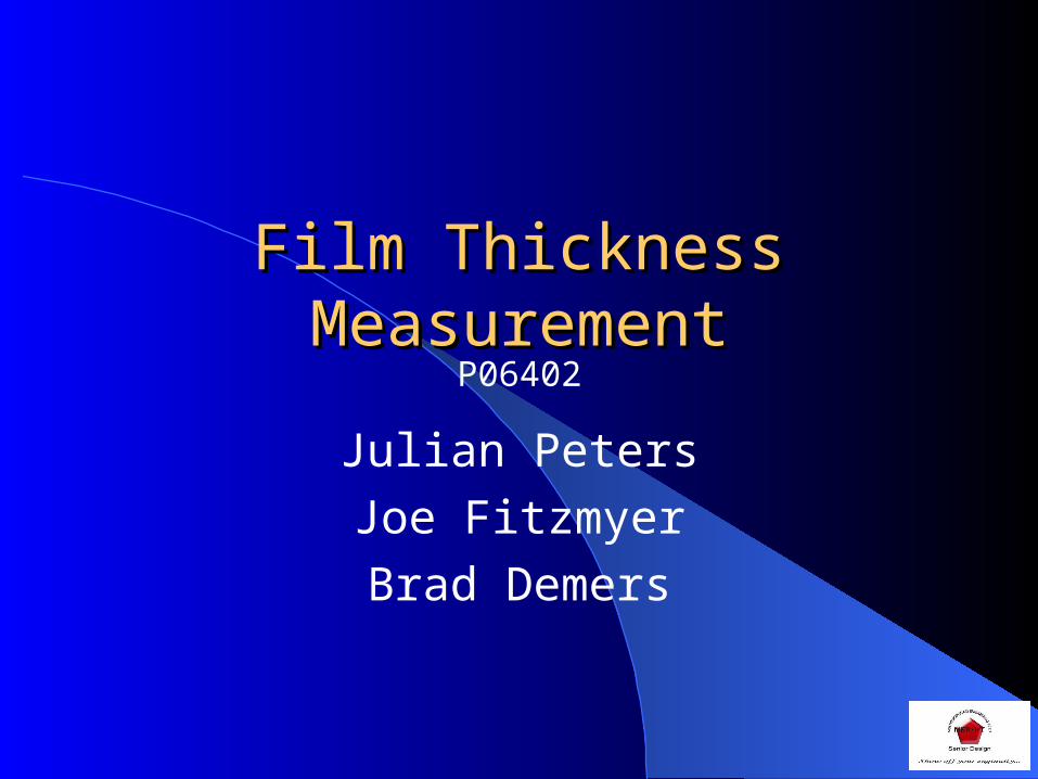
Film Thickness MeasurementFilm Thickness Measurement
Julian Peters
Joe Fitzmyer
Brad Demers
P06402
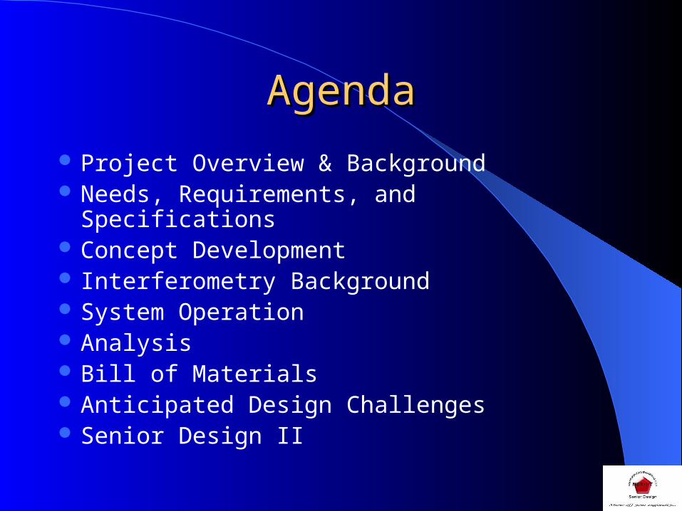
AgendaAgenda
Project Overview & Background Needs, Requirements, and Specifications Concept Development Interferometry Background System Operation Analysis Bill of Materials Anticipated Design Challenges Senior Design II
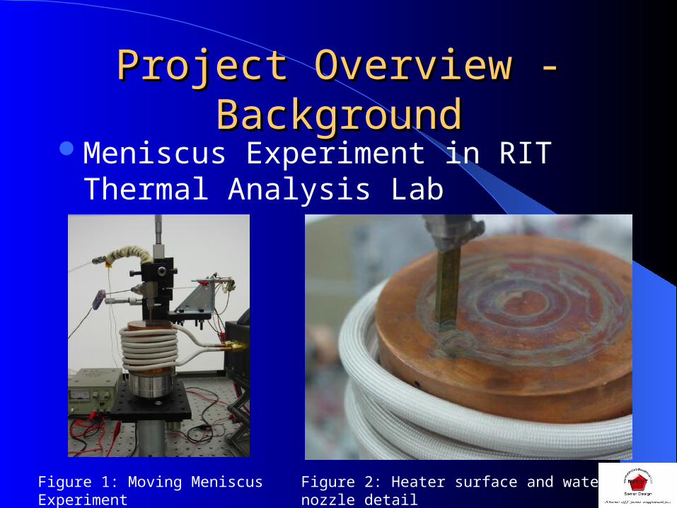
Project Overview - Project Overview - BackgroundBackground
Meniscus Experiment in RIT Thermal Analysis Lab
Figure 1: Moving Meniscus Experiment Figure 2: Heater surface and water nozzle detail
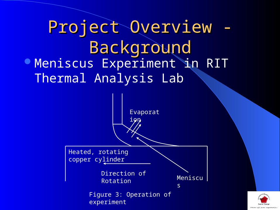
Project Overview - Project Overview - BackgroundBackground
Meniscus Experiment in RIT Thermal Analysis Lab
Figure 3: Operation of experiment
Heated, rotating copper cylinder
Meniscus
Evaporation
Direction of Rotation
Project Overview - Project Overview - BackgroundBackground
Meniscus Experiment in RIT Thermal Analysis Lab – Unanswered Questions:– Is there a film of adsorbed water left behind the
moving meniscus?– How far does it extend?– What is its thickness?
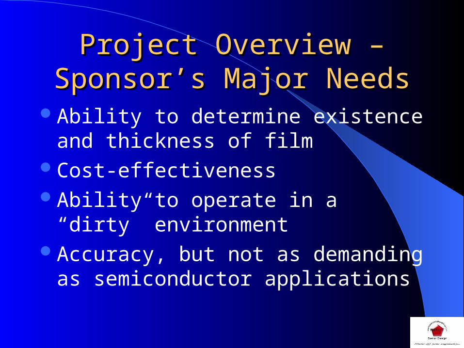
Project Overview – Sponsor’s Project Overview – Sponsor’s Major NeedsMajor Needs
Ability to determine existence and thickness of film
Cost-effectivenessAbility to operate in a “dirty” environmentAccuracy, but not as demanding as
semiconductor applications
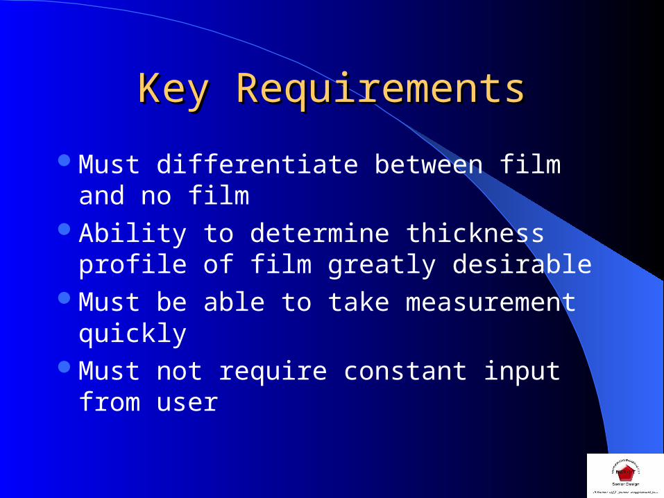
Key RequirementsKey Requirements
Must differentiate between film and no filmAbility to determine thickness profile of
film greatly desirableMust be able to take measurement quicklyMust not require constant input from user
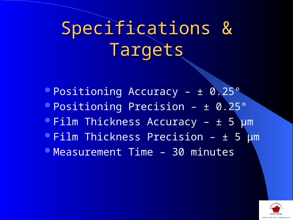
Specifications & TargetsSpecifications & Targets
Positioning Accuracy – ± 0.25°Positioning Precision – ± 0.25°Film Thickness Accuracy – ± 5 μmFilm Thickness Precision – ± 5 μmMeasurement Time – 30 minutes
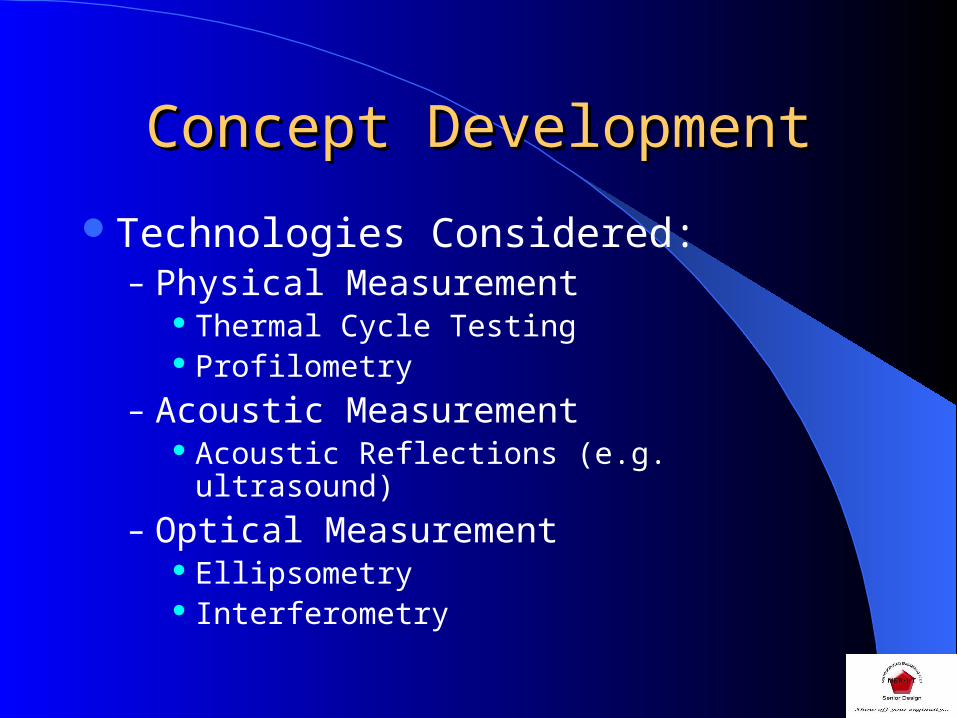
Concept DevelopmentConcept Development
Technologies Considered:– Physical Measurement
Thermal Cycle Testing Profilometry
– Acoustic Measurement Acoustic Reflections (e.g. ultrasound)
– Optical Measurement Ellipsometry Interferometry
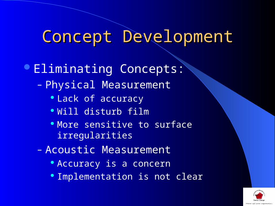
Concept DevelopmentConcept Development
Eliminating Concepts:– Physical Measurement
Lack of accuracy Will disturb film More sensitive to surface irregularities
– Acoustic Measurement Accuracy is a concern Implementation is not clear
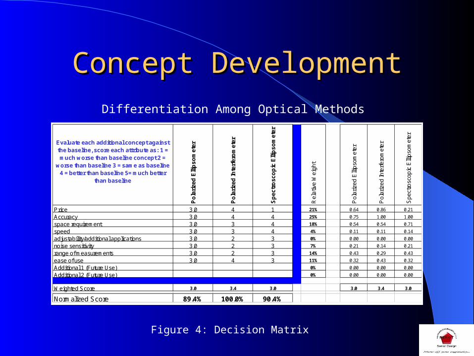
Concept DevelopmentConcept Development
Evaluate each additional concept against the baseline, score each attribute as: 1 = much worse than baseline concept 2 =
worse than baseline 3 = same as baseline 4 = better than baseline 5= much better
than baseline
Po
lari
zed
Elli
ps
om
ete
r
Po
lari
zed
Inte
rfe
rom
ete
r
Sp
ec
tro
sc
op
ic E
llip
so
me
ter
Re
lativ
e W
eig
ht
Po
lari
zed
Elli
pso
me
ter
Po
lari
zed
Inte
rfe
rom
ete
r
Sp
ect
rosc
op
ic E
llip
som
ete
r
Price 3.0 4 1 21% 0.64 0.86 0.21
Accuracy 3.0 4 4 25% 0.75 1.00 1.00
space requirement 3.0 3 4 18% 0.54 0.54 0.71
speed 3.0 3 4 4% 0.11 0.11 0.14
adjustability/additional applications 3.0 2 3 0% 0.00 0.00 0.00
noise sensitivity 3.0 2 3 7% 0.21 0.14 0.21
range of measurements 3.0 2 3 14% 0.43 0.29 0.43
ease of use 3.0 4 3 11% 0.32 0.43 0.32
Additional 1 (Future Use) 0% 0.00 0.00 0.00
Additional 2 (Future Use) 0% 0.00 0.00 0.00
Weighted Score 3.0 3.4 3.0 3.0 3.4 3.0
Normalized Score 89.4% 100.0% 90.4%
Differentiation Among Optical Methods
Figure 4: Decision Matrix
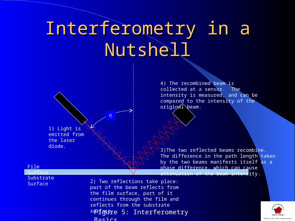
i
Film Surface
Substrate Surface
1) Light is emitted from the laser diode.
2) Two reflections take place: part of the beam reflects from the film surface, part of it continues through the film and reflects from the substrate surface.
3)The two reflected beams recombine. The difference in the path length taken by the two beams manifests itself as a phase difference, which can cause attenuation of the beam intensity.
4) The recombined beam is collected at a sensor. The intensity is measured, and can be compared to the intensity of the original beam.
Interferometry in a NutshellInterferometry in a Nutshell
Figure 5: Interferometry Basics
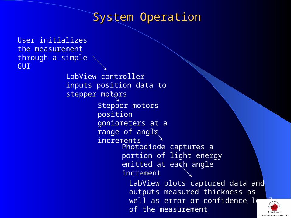
System OperationSystem Operation
User initializes the measurement through a simple GUI
Stepper motors position goniometers at a range of angle increments
Photodiode captures a portion of light energy emitted at each angle increment
LabView controller inputs position data to stepper motors
LabView plots captured data and outputs measured thickness as well as error or confidence level of the measurement
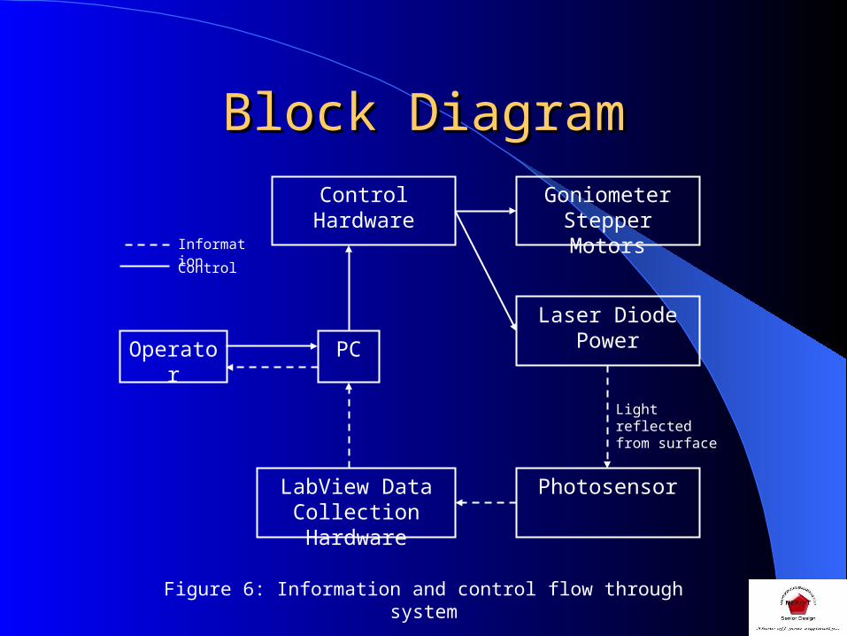
Block DiagramBlock Diagram
Figure 6: Information and control flow through system
PC
Control Hardware Goniometer Stepper Motors
Laser Diode Power
PhotosensorLabView Data Collection Hardware
Operator
Light reflected from surface
Information
Control
Motors Goniometers
Laser diode
Photodiode
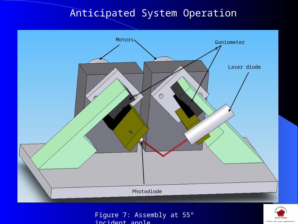
Anticipated System Operation
Figure 7: Assembly at 55° incident angle
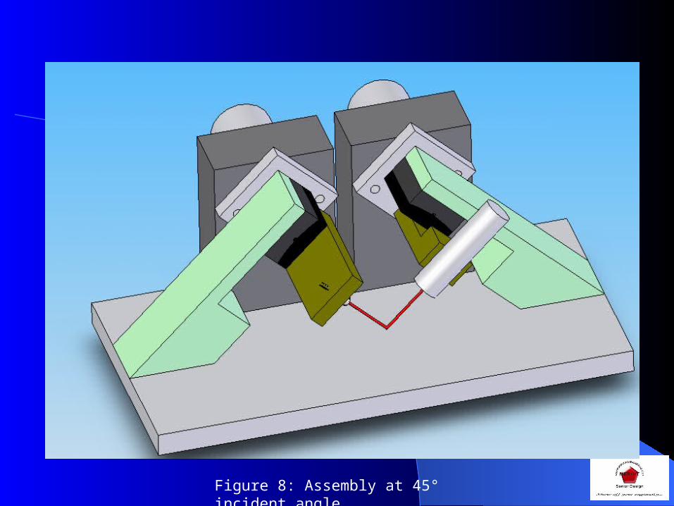
Figure 8: Assembly at 45° incident angle
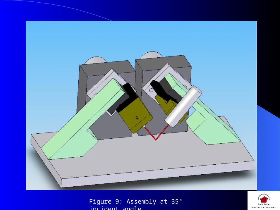
Figure 9: Assembly at 35° incident angle
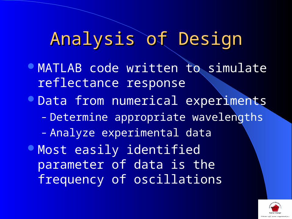
Analysis of DesignAnalysis of Design
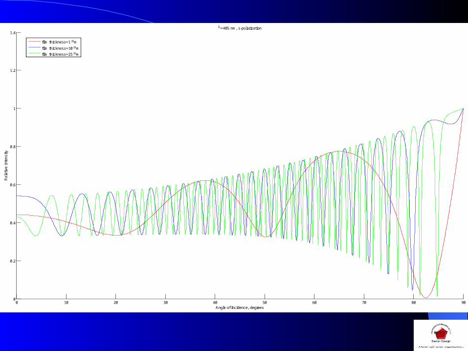
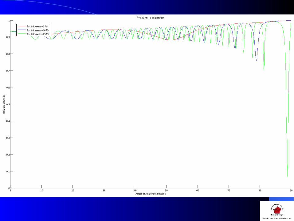
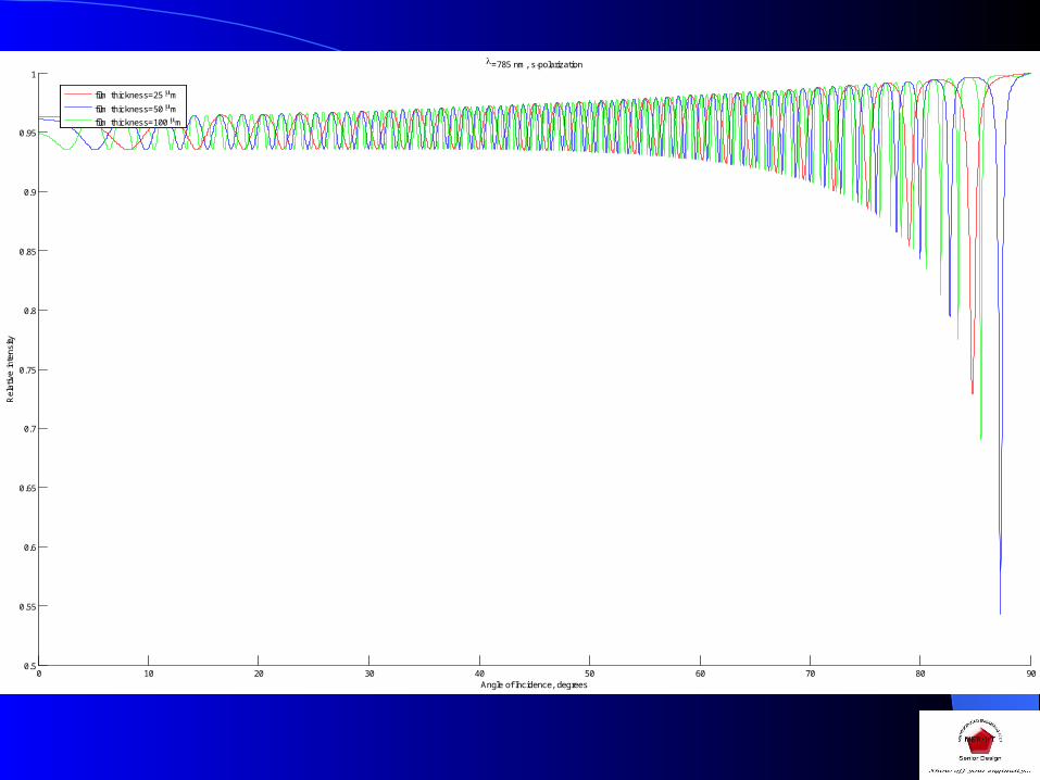
MATLAB code written to simulate reflectance response
Data from numerical experiments– Determine appropriate wavelengths– Analyze experimental data
Most easily identified parameter of data is the frequency of oscillations
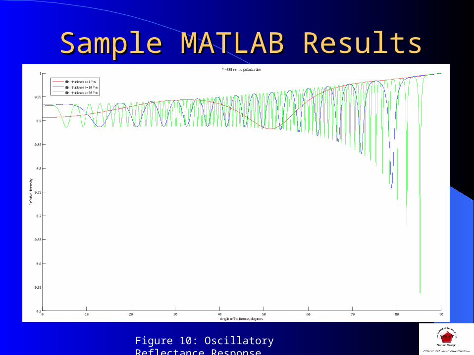
Sample MATLAB ResultsSample MATLAB Results
0 10 20 30 40 50 60 70 80 900.5
0.55
0.6
0.65
0.7
0.75
0.8
0.85
0.9
0.95
1
Angle of Incidence, degrees
Rel
ativ
e in
tens
ity
=635 nm, s-polarization
film thickness=1 m
film thickness=10 m
film thickness=50 m
Figure 10: Oscillatory Reflectance Response
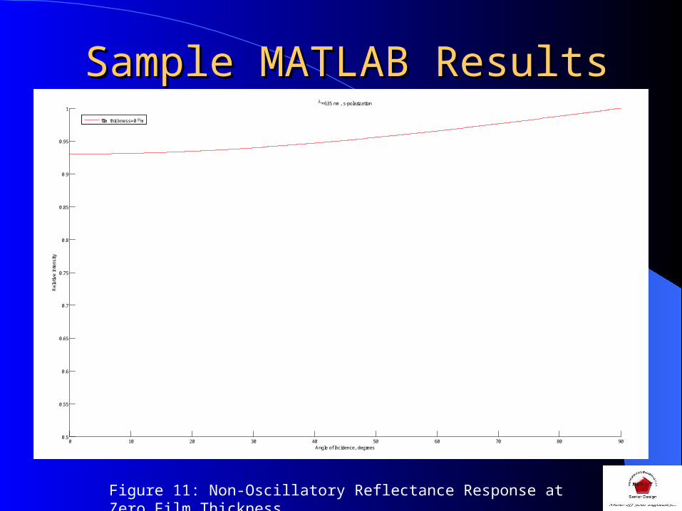
Sample MATLAB ResultsSample MATLAB Results
0 10 20 30 40 50 60 70 80 900.5
0.55
0.6
0.65
0.7
0.75
0.8
0.85
0.9
0.95
1
Angle of Incidence, degrees
Rel
ativ
e in
tens
ity
=635 nm, s-polarization
film thickness=0 m
Figure 11: Non-Oscillatory Reflectance Response at Zero Film Thickness
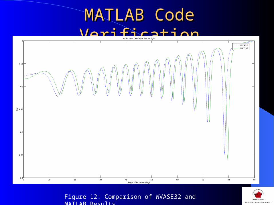
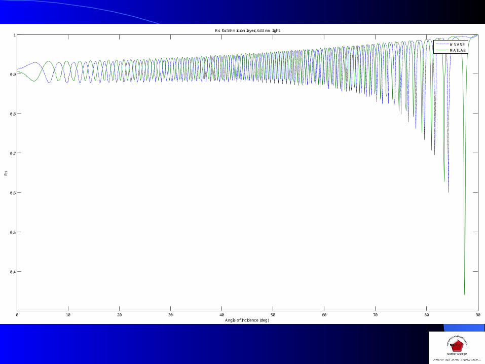
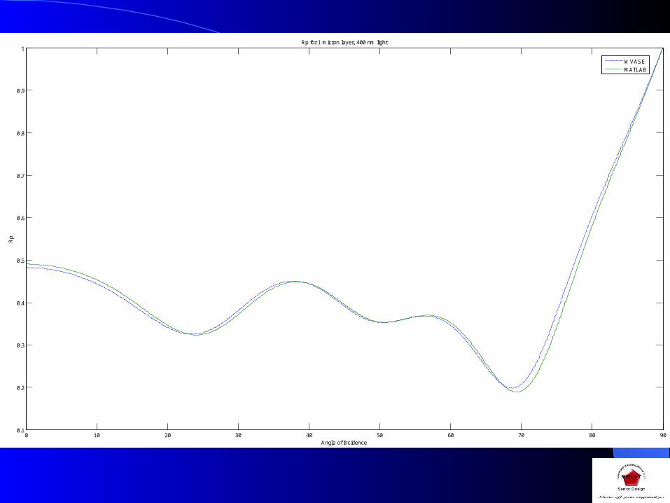
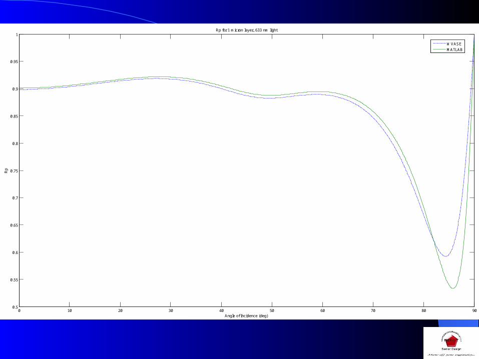
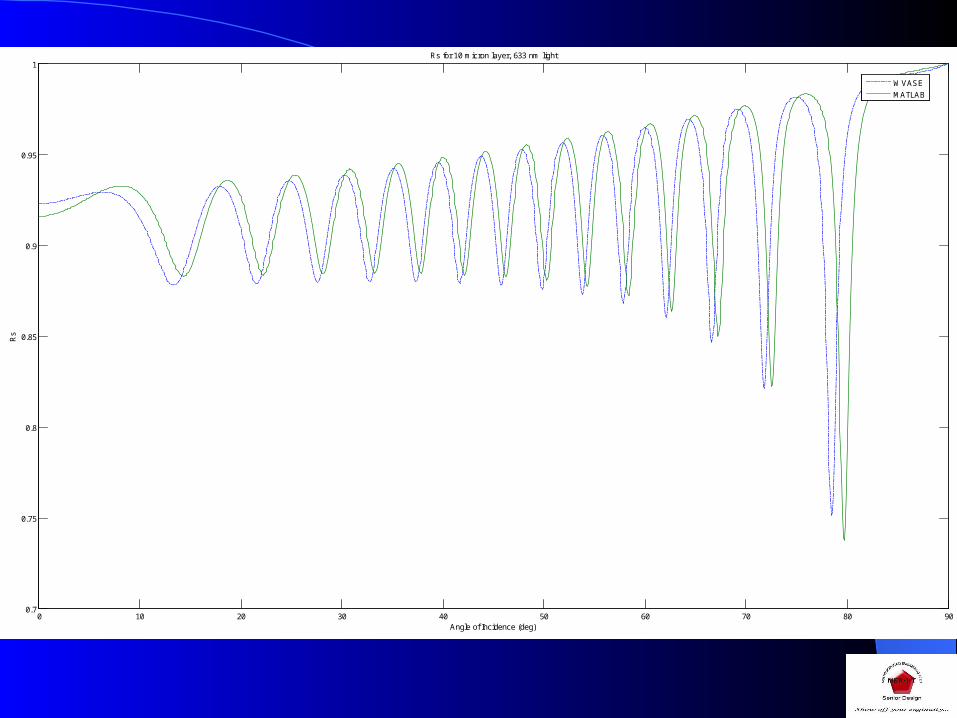
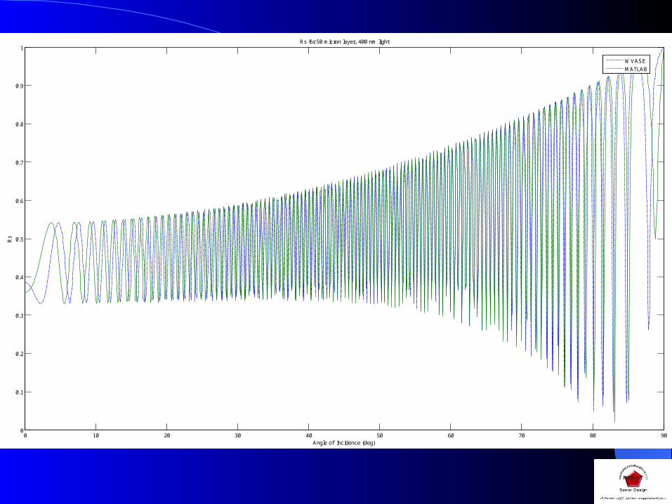
MATLAB Code VerificationMATLAB Code Verification
0 10 20 30 40 50 60 70 80 900.7
0.75
0.8
0.85
0.9
0.95
1
Angle of Incidence (deg)
Rs
Rs for 10 micron layer, 633 nm light
WVASE
MATLAB
Figure 12: Comparison of WVASE32 and MATLAB Results
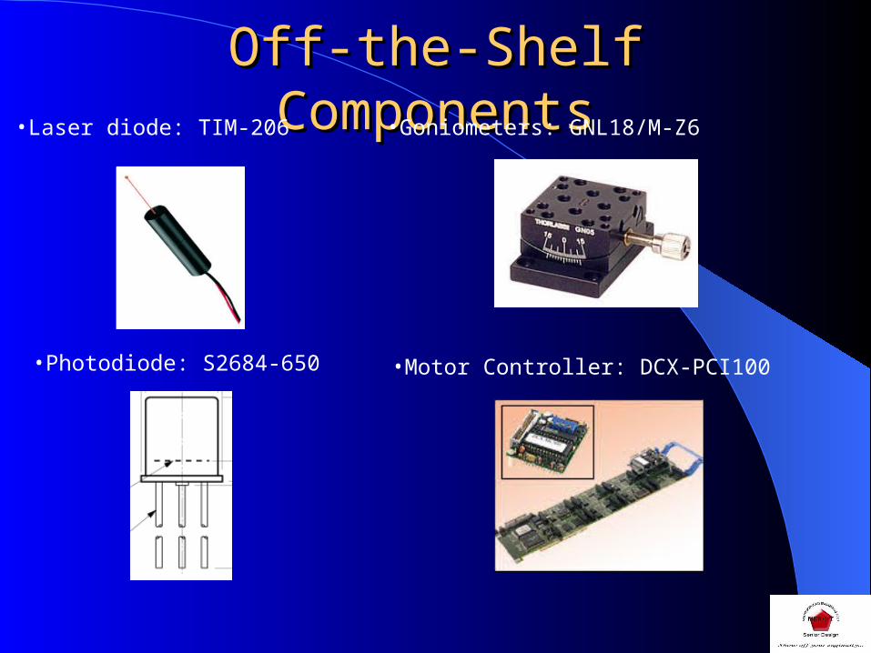
Off-the-Shelf ComponentsOff-the-Shelf Components•Laser diode: TIM-206 •Goniometers: GNL18/M-Z6
•Photodiode: S2684-650 •Motor Controller: DCX-PCI100
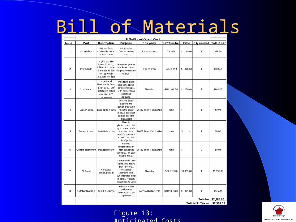
Bill of MaterialsBill of Materials
Figure 13: Anticipated Costs
Item # Part Description Purpose Company Part Number Price Qty needed Total Cost
1 Laser Diode650 nm laser
diode with 10mW output power
Emits beam focused on one
spot.Laser Dreams TIM-206 60.00$ 1 $60.00
2 Photodiode
High Sensitive Monochromatic
Silicon Pin diode. Sensitive to 650
nm light with interference filter
Measures power of reflected beam. Outputs measured
voltage.
Hamamatsu S2684-650 108.60$ 1 $108.60
3 Goniometer
Large Metric Mount with focus
1.75" away. 200
rotation in either
direction in 10
increments
Positions laser and sensor at a range of angles, with same focal
point and distance.
Thorlabs GNL18/M-Z6 450.00$ 2 $900.00
4 Laser Mount laser diode mount
Mounts laser diode to the
goniometer such that the laser
module does not extend past the
focal point
06402 Team Fabrication none -$ 1 $0.00
5 Sensor Mount photodiode mount
Mounts photodiode to the goniometer such
that the diode module does not extend past the
focal point
06402 Team Fabrication none -$ 1 $0.00
6 Goniometer Mount Position mount
Mounts goniometer with high positional
accuracy. Will be built to table.
06402 Team Fabrication none -$ 2 $0.00
7 PCI cardMotorized
controller card
Understands user inputs and relays them to motor.
Accurately postions and
synchronizes both motors. Reports data back to user
Thorlabs DCX-PCI100 1,195.00$ 1 $1,195.00
8 Multifunction DAQ 12-bit resolution
relays position and power
information to the operator
National Instruments NI-USB-6009 125.00$ 1 $125.00
$2,388.60$2,591.63
Bill of Materials and Cost
Total -->Total with Tax -->
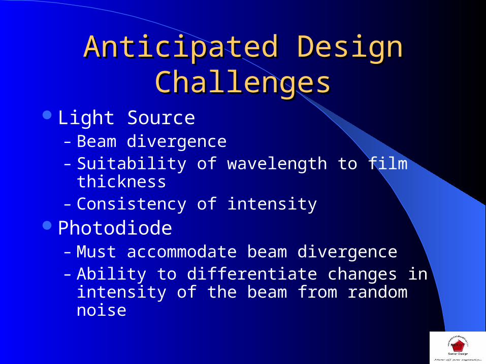
Anticipated Design Anticipated Design ChallengesChallenges
Light Source– Beam divergence– Suitability of wavelength to film thickness– Consistency of intensity
Photodiode– Must accommodate beam divergence– Ability to differentiate changes in intensity of
the beam from random noise
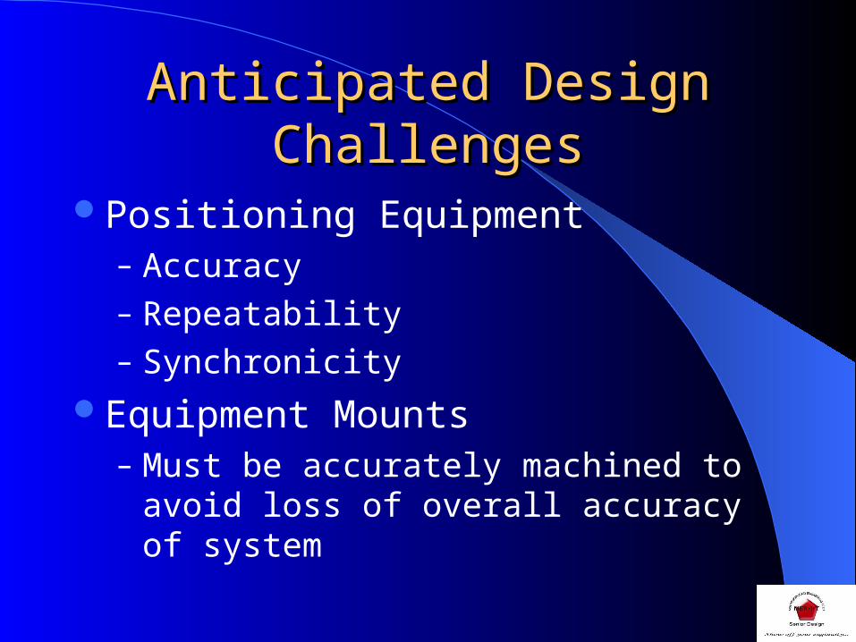
Anticipated Design Anticipated Design ChallengesChallenges
Positioning Equipment– Accuracy– Repeatability– Synchronicity
Equipment Mounts– Must be accurately machined to avoid loss of
overall accuracy of system
Anticipated Design Anticipated Design ChallengesChallenges
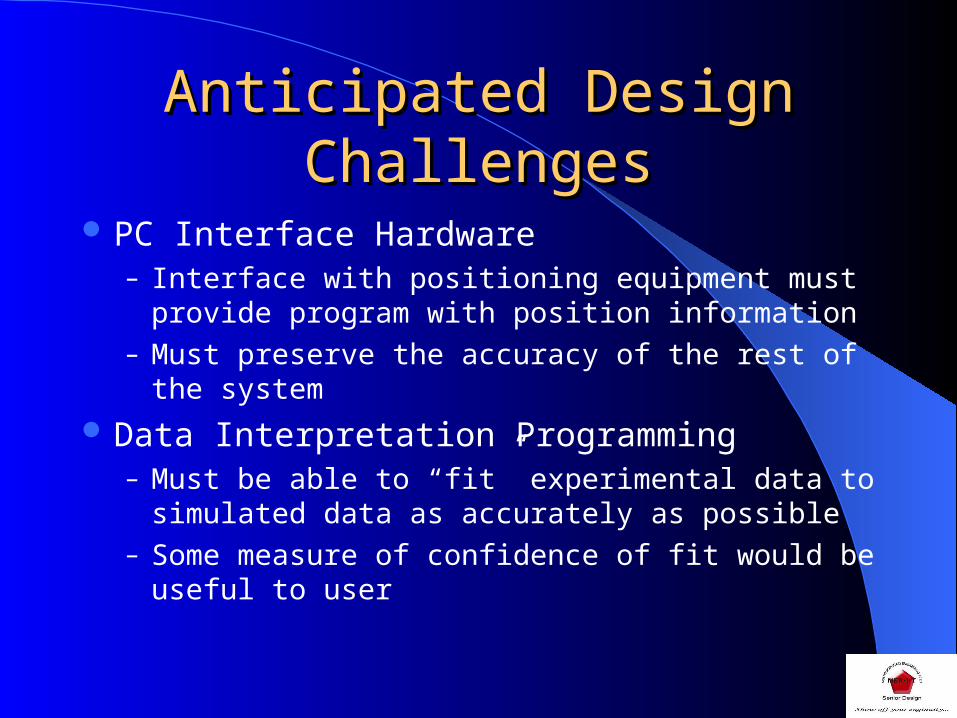
PC Interface Hardware– Interface with positioning equipment must provide
program with position information– Must preserve the accuracy of the rest of the system
Data Interpretation Programming– Must be able to “fit” experimental data to simulated
data as accurately as possible– Some measure of confidence of fit would be useful to
user
Anticipated Design Anticipated Design ChallengesChallenges
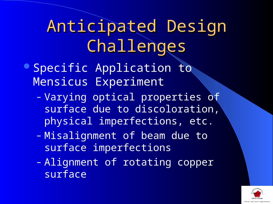
Specific Application to Mensicus Experiment– Varying optical properties of surface due to
discoloration, physical imperfections, etc.– Misalignment of beam due to surface
imperfections– Alignment of rotating copper surface

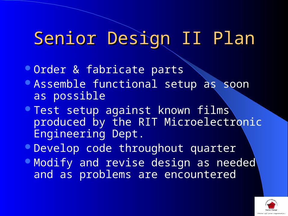
Senior Design II PlanSenior Design II Plan
Order & fabricate partsAssemble functional setup as soon as
possibleTest setup against known films produced by
the RIT Microelectronic Engineering Dept.Develop code throughout quarterModify and revise design as needed and as
problems are encountered
Senior Design II PlanSenior Design II Plan
Order & fabricate partsAssemble functional setup as soon as
possibleTest setup against known films produced by
the RIT Microelectronic Engineering Dept.Develop code throughout quarterModify and revise design as needed and as
problems are encountered

Senior Design II ScheduleSenior Design II Schedule
Week 3 Week 4
Test System
Receive Ordered PartsMachine Team-Manufactured Parts
Write Control and DAQ CodeAssemble System
Week 9 Week 10
Week 5
Week 6 Week 7 Week 8
Week 1 Week 2
Write Reports, etc.
Write Control and DAQ CodeAssemble System
Test SystemRun Meniscus Tests
Figure 14: Senior Design II Gantt Chart
Any Questions?Any Questions?
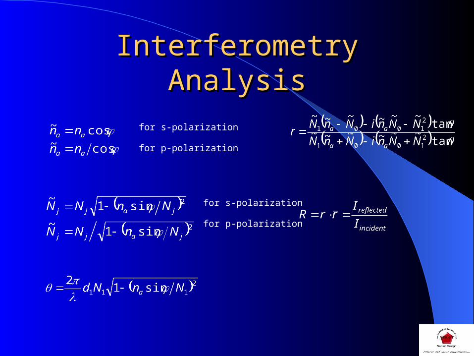
Interferometry AnalysisInterferometry Analysis
for s-polarization
for p-polarization
for s-polarization
for p-polarization
0 10 20 30 40 50 60 70 80 900
0.2
0.4
0.6
0.8
1
1.2
1.4
Angle of Incidence, degrees
Rel
ativ
e in
tens
ity
=405 nm, s-polarization
film thickness=1 m
film thickness=10 m
film thickness=25 m
0 10 20 30 40 50 60 70 80 900
0.1
0.2
0.3
0.4
0.5
0.6
0.7
0.8
0.9
1
Angle of Incidence, degrees
Rel
ativ
e in
tens
ity
=635 nm, s-polarization
film thickness=1 m
film thickness=10 m
film thickness=25 m
0 10 20 30 40 50 60 70 80 900.5
0.55
0.6
0.65
0.7
0.75
0.8
0.85
0.9
0.95
1
Angle of Incidence, degrees
Rel
ativ
e in
tens
ity
=785 nm, s-polarization
film thickness=25 m
film thickness=50 m
film thickness=100 m
0 10 20 30 40 50 60 70 80 900.75
0.8
0.85
0.9
0.95
1
Angle of Incidence, degrees
Rel
ativ
e in
tens
ity
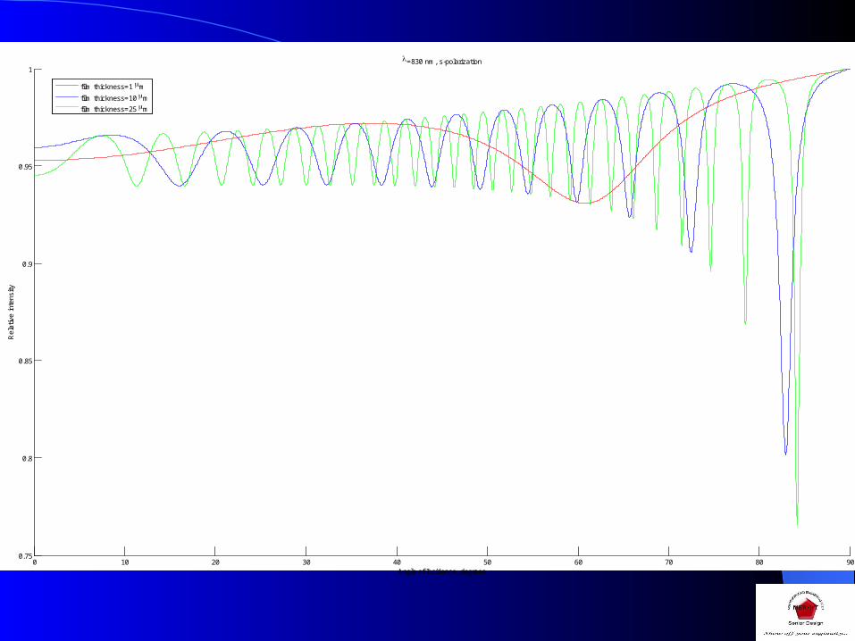
=830 nm, s-polarization
film thickness=1 m
film thickness=10 m
film thickness=25 m
0 10 20 30 40 50 60 70 80 90
0.4
0.5
0.6
0.7
0.8
0.9
1
Angle of Incidence (deg)
Rs
Rs for 50 micron layer, 633 nm light
WVASE
MATLAB
0 10 20 30 40 50 60 70 80 900.1
0.2
0.3
0.4
0.5
0.6
0.7
0.8
0.9
1
Angle of Incidence
Rp
Rp for 1 micron layer, 400 nm light
WVASE
MATLAB
0 10 20 30 40 50 60 70 80 900.5
0.55
0.6
0.65
0.7
0.75
0.8
0.85
0.9
0.95
1
Angle of Incidence (deg)
Rp
Rp for 1 micron layer, 633 nm light
WVASE
MATLAB
0 10 20 30 40 50 60 70 80 900
0.1
0.2
0.3
0.4
0.5
0.6
0.7
0.8
0.9
1
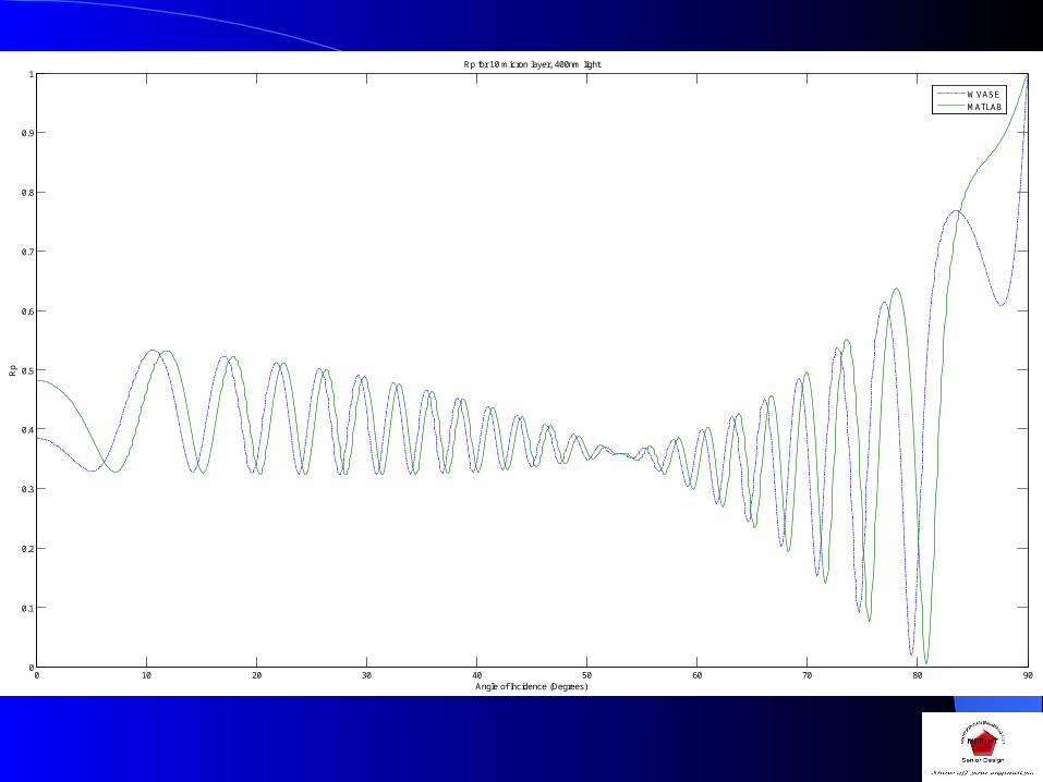
Angle of Incidence (Degrees)
Rp
Rp for 10 micron layer, 400nm light
WVASE
MATLAB

0 10 20 30 40 50 60 70 80 900.4
0.5
0.6
0.7
0.8
0.9
1
Angle of Incidence
Rp
Rp for 10 micron layer, 633 nm light
WVASE
MATLAB
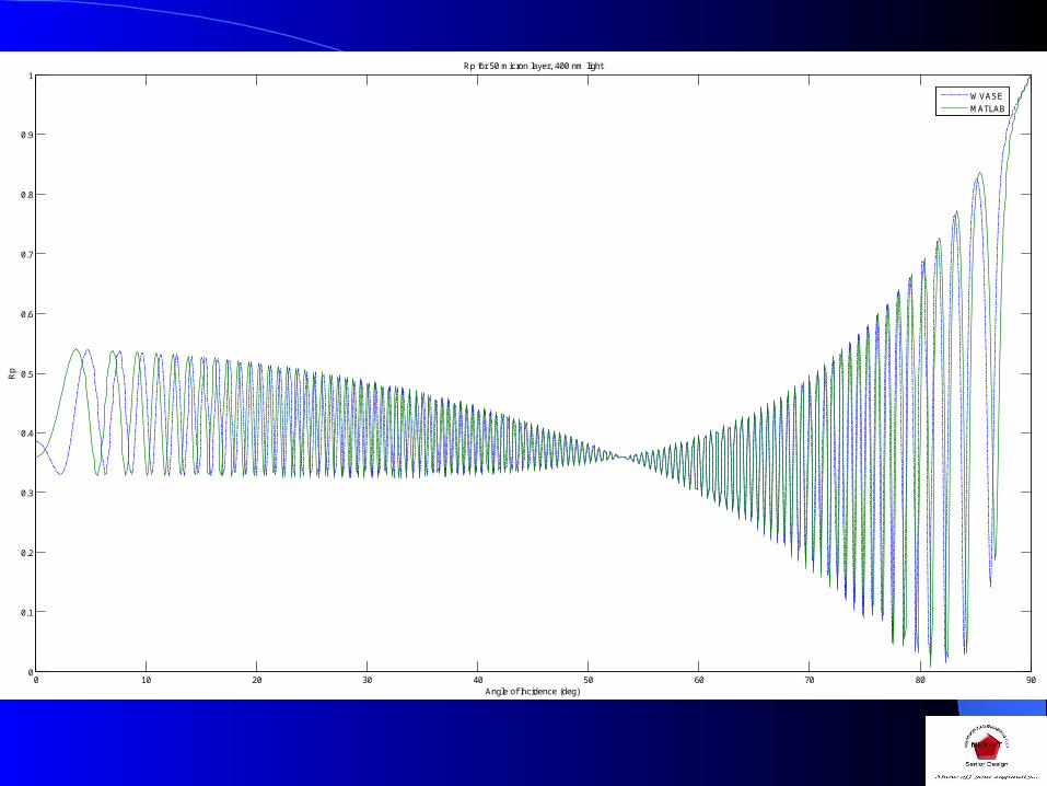
0 10 20 30 40 50 60 70 80 900
0.1
0.2
0.3
0.4
0.5
0.6
0.7
0.8
0.9
1
Angle of Incidence (deg)
Rp
Rp for 50 micron layer, 400 nm light
WVASE
MATLAB

0 10 20 30 40 50 60 70 80 900.2
0.3
0.4
0.5
0.6
0.7
0.8
0.9
1
Angle of Incidence (deg)
Rp
Rp for 50 micron layer, 633 nm light
WVASE
MATLAB

0 10 20 30 40 50 60 70 80 900
0.1
0.2
0.3
0.4
0.5
0.6
0.7
0.8
0.9
1
Angle of Incidence (deg)
Rs
Rs for 1 micron layer, 400 nm light
WVASE
MATLAB
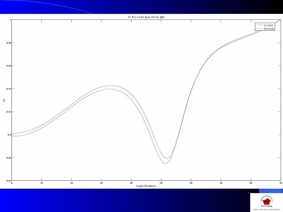
0 10 20 30 40 50 60 70 80 900.86
0.88
0.9
0.92
0.94
0.96
0.98
1
Angle of Incidence
Rs
Rs for 1 micron layer, 633 nm light
WVASE
MATLAB
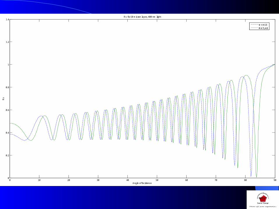
0 10 20 30 40 50 60 70 80 900
0.2
0.4
0.6
0.8
1
1.2
1.4
Angle of Incidence
Rs
Rs for 10 micron layer, 400 nm light
WVASE
MATLAB
0 10 20 30 40 50 60 70 80 900.7
0.75
0.8
0.85
0.9
0.95
1
Angle of Incidence (deg)
Rs
Rs for 10 micron layer, 633 nm light
WVASE
MATLAB
0 10 20 30 40 50 60 70 80 900
0.1
0.2
0.3
0.4
0.5
0.6
0.7
0.8
0.9
1
Angle of Incidence (deg)
Rs
Rs for 50 micron layer, 400 nm light
WVASE
MATLAB


![JOSEPH A. FITZMYER (1920) DOMANDE SU GESU – LE RISPOSTE DEL NUOVO TESTAMENTO [orig. 1982] QUERINIANA, BRESCIA 1987](https://img.pdfslide.us/doc/110x75/5542eb59497959361e8c50c6/joseph-a-fitzmyer-1920-domande-su-gesu-le-risposte-del-nuovo-testamento-orig-1982-queriniana-brescia-1987.jpg)