Embed Size (px)
Citation preview

Lecture 8 - Integrated Optics in Comms. Systems
Up to now we've looked at various discrete elements of �bre communication sys-
tems, including lasers, detectors and �bres. In this lecture I shall be looking at the physics
of elements required to pull all these together in an integrated system. These elements
include �bre couplers, mixers and splitters, waveguides for integrated optics and elements
for multiplexing and de-muliplexing �bres using di�erent wavelength channels. Finally I
shall look at the use of solitons, which were introduced in an earlier lecture, in commercial
transmission systems.
1 Fibre Connectors, Couplers, Mixers and Splitters
1.1 Fibre Connectors
Although �bres are produced on large drums many kilometres long, when used in a
communication circuit they inevitably have to be joined or connected together. This
must be done in such a way as to minimize the loss at each connection, otherwise the
entire system would become too lossy.
Perhaps the simplest technique for permanently joining �bres together is to use a
fusion splice. Here (�gure 8.1) the �bre ends are held in close proximity and heated up to
the material softening point (� 2300K in silica). The �bres are then pushed together and
the two ends fuse to form a continuous length of �bre. The joint is weak and is usually
protected by a resin or epoxy overcoat and a metal cover. Both singe and multimode
�bre can be joined in this way, with losses as small as 0:1 dB common.
Sometimes it is impractical to use a fusion splice, where a �bre enters a repeater
for example, and a demountable connector is necessary. Unfortunately the use of connec-
tors inevitably introduces losses into the system. These are of two main types: Fresnel
losses, caused by back re ection at the silica/air interfaces, and losses associated with
misalignment of the end faces. The re ectance of a �bre at normal incidence is:
RF =
�n1 � n0
n1 + n0
�2
where n0 is the refractive index of the medium between the �bres and n1 is that of the
�bre core. For silica �bre, n1 = 1:48 so we have:
RF =
�1:48� 1
1:48 + 1
�2
= 0:0375:
1

Figure 8.1 In fusion splicing, the fibre ends are pushed together whilst being heated within an electric arc.
Figure 8.2 Illustration of the three types of misalignment mentioned in the text:(a) longitudinal; (b) lateral and (c) angular misalignment. The parameters usedto describe these (S, D and α) are also shown.
Thus the transmission is 1�0:0375 = 0:9625. This corresponds to a loss of�10 log(0:9625) =
0:17 dB.
The second type of loss associated with butt-type connections arises from misalign-
ment between the �bres. There are three basic type to be considered: (a) the distance
between the �bres along the �bre axis (longitudinal); (b) the o�set distance perpendicular
to the �bre axis (lateral); and (c) the angle between the two axes of the �bres (angular).
These are illustrated in �gure 8.2. Lateral loss is the most signi�cant, the transmission
losses resulting from lateral misalignment can be written:
Tlat =2
�
8<:cos�1
�D
2a
��
D
2a
"1�
�D
2a
�2#1=29=
;where D is the lateral displacement and a the �bre core radius. As an example consider
a multimode step index �bre with a lateral misalignment of 10% of the �bre diameter.
Thus D=2a = 0:1. The transmission becomes:
Tlat =2
�
ncos�1(0:1)� 0:1[1� (0:1)2]1=2
o= 0:873
and the transmission loss is therefore �10 log(0:873) = 0:59 dB. If Fresnel losses from the
example above were also added, the total loss would be 0:17 + 0:59 = 0:76 dB. A typical
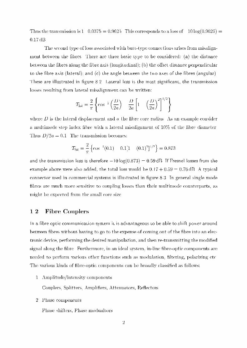
connector used in commercial systems is illustrated in �gure 8.3. In general single mode
�bres are much more sensitive to coupling losses than their multimode counterparts, as
might be expected from the small core size.
1.2 Fibre Couplers
In a �bre optic communication system it is advantageous to be able to shift power around
between �bres without having to go to the expense of coming out of the �bre into an elec-
tronic device, performing the desired manipulation, and then re-transmitting the modi�ed
signal along the �bre. Furthermore, in an ideal system, in-line �bre-optic components are
needed to perform various other functions such as modulation, �ltering, polarizing etc.
The various kinds of �bre-optic components can be broadly classi�ed as follows:
1. Amplitude/intensity components
Couplers, Splitters, Ampli�ers, Attenuators, Re ectors
2. Phase components
Phase shifters, Phase modualtors
2
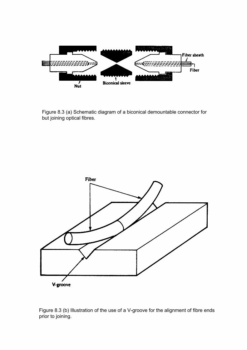
Figure 8.3 (a) Schematic diagram of a biconical demountable connector forbut joining optical fibres.
Figure 8.3 (b) Illustration of the use of a V-groove for the alignment of fibre endsprior to joining.

3. Polarization components
Polarizers, Polarization splitters, Polarization controllers
4. Wavelength components
Wavelength �lters, Wavelength division multiplexers/demultiplexers
5. Frequency components
Frequency shifters, Filters
6. Active components
Fibre ampli�ers
In this part of the lecture I will look at the principles behind the operation of some
of the above devices. A fuller description can be found in Introduction to Fiber Optics
by A. Ghatak and K. Thyagarajan.
1.3 The Optical Fibre Directional Coupler
The optical �bre directional coupler is the guided wave equivalent of a bulk optic beam
splitter and is one of the most important in-line �bre components. It is based on the fact
that the modal �eld of the guided mode extends far beyond the core-cladding interface.
Thus when two �bre cores are brought su�ciently close to each other laterally, so that
their modal �elds overlap, then the modes of the two �bres become coupled and power
can transfer periodically between the two �bres. If the propagation constants of the
modes of the individual �bres are equal, then this power exchange is complete. On the
other hand, if their propagation constants are di�erent, then there is still a periodic, but
incomplete, exchange of power between the �bres.
Directional couplers have many interesting applications in power splitting, wave-
length division multiplexing/demultiplexing, polarization splitting, �bre optic sensing
and so forth.
Consider a directional coupler formed of two, in general, nonidentical single-mode
�bres supporting the LP01 modes with propagation constants �1 and �2. It can be shown
(after much algebra!) that if P1(0) is the power launched into �bre 1 at z = 0, then at
any value of z the powers propagating in the two �bres are:
P1(z)
P1(0)= 1�
�2
2sin2 z
3

P2(z)
P1(0)=
�2
2sin2 z
where
2 = �
2 +1
4(��)2
and
�� = �1 � �2
In the above equations � is called the coupling coe�cient and is a measure of the
strength of the interaction between the two �bres, which depends on the �bre parameters,
the separation of the cores and the wavelength of operation. The parameter � is referred
to as the phase mismatch. Note that, from above,
P1(z) + P2(z) = P1(0)
independent of z. This is nothing but a statement of conservation of power.
If the two �bres are separated by a distance which is large compared with the
mode size then there is now interaction between them. In this case � = 0 and we have
P1(z) = P1(0) P2(z) = 0
Now consider the two cases of phase matching and non-phase matching.
1.3.1 Phase matched case
Assume that the �bres are identical. Then if �� = 0 we get
P1(z) = P1(0) cos2�z
P2(z) = P1(0) sin2�z
Figure 8.4 shows the variation of the powers in the two �bres as a function of z.
There is a periodic exchange of power between the two �bres, and when
z = 0;�
�
;
2�
�
; : : : =m�
�
; m = 0; 1; 2; : : :
P1(z) = P1(0) and P2(z) = 0 | that is, the entire power is in the input �bre. When
z =�
2�;
3�
2�;
5�
2�; : : :
=
�m+
1
2
��
�
; m = 0; 1; 2; : : :
4

P1(z) = 0 and P2(z) = P1(0) and the entire power is in the other �bre. The minimum
distance at which the power completely transfers from the input �bre to the other �bre
is given by
z = Lc =�
2�
and is referred to as the coupling length. Strong interaction implies a large value of �
and, hence, a small coupling length.
For typical single-mode �bres operating at a wavelength of 1:3�m, � � 0:8mm�1
to 0:3mm�1, leading to a coupling length of � 2� 5mm.
1.3.2 Non-phase matched case
Here �1 6= �2. The equations governing the relative power in each �bre do not simplify
in this case so we'll look at some speci�c values of ��=2�. The variation of P2(z) for
��=2� = 0:1; 1 and 5 are plotted in �gure 8.5. From the �gure we note that:
� If �� 6= 0, there is an incomplete transfer of power. In fact the maximum fractional
power that is transferred from the input �bre to the coupled �bre is given by
�max =P2;max
P1(0)=
�2
2sin2 z
!max
=�2
2=
1
1 + (��=2�)
Thus, for complete power exchange, we must have �� = 0; the larger the ratio
��=2� the smaller is the fractional power transfer. For example, for ��=2� =
0:1; 1 and 5, the maximum fractional power transferred is 0.99, 0.5 and 0.04. Hence
very little transfer of power will take place between two highly non-phase-matched
�bres, even if their cores lie close to each other as long as ��=2�� 1.
� Note also from �gure 8.5 that for larger ��=2� values, the oscillations in power
become more and more rapid in z. This e�ect is used in integrated optics for re-
alizing optical switches, in wavelength multiplexers/demultiplexers, in polarization
splitting using birefringent �bres and so on.
Figure 8.6(a) shows a three dimensional plot of variation in the transverse intensity
pattern along the propagation direction for a pair of identical planar waveguides. The
corresponding density plot clearly showing complete power transfer is shown in �gure
8.6(b). Figures 8.7(a) and (b) show the corresponding plots for a pair of non-identical
planar waveguides.
5

Figure 8.4 Variation of powers in the two fibres in a directional coupler asa function of z when the two fibres have the same propagation constant.
Figure 8.5 Variation of power in the coupled fibre plotted as a function of κz for different values of relative phase mismatch ∆β/2κ. For ∆β ≠ 0, the power transfer is always incomplete. The larger the value of ∆β/2κ, the smaller is the fractional power transfer. The three curves correspond to ∆β/2κ = 0.1 (long dash), 1.0 (small dash) and 5.0 (solid).

(a)
(b)
Figure 8.6 (a) Three-dimensional plot of variation of power with propagation length in a directional coupler with ∆β = 0. Note that the power exchange between the two waveguides (WG1 and WG2) is complete. (b) The corresponding density plot.

1.3.3 Practical parameters of a coupler
If power Pi is launched into the input port of a directional coupler as shown in �gure 8.8
and if the transmitted power, coupled power and back-coupled power are Pt; Pc; and Pr,
respectively, then the various characteristics of the coupler are:
Coupling ratio R(%) =Pc
Pc + Pt� 100
R(dB) = 10 log
�Pt + Pc
Pc
�
Excess loss Li(dB) = 10 log
�Pi
Pt + Pc
�
Insertion loss = 10 log
�Pi
Pc
�
= Coupling ratio + excess loss
Directivity D(dB) = 10 log
�Pr
Pi
�
Good directional couplers have low insertion loss and high directivity. Commercially
available directional couplers have coupling ratios from 50/50 to 1/99, excess loss� 3:4 dB
(for 3-dB coupler), and directivity of better than �55 dB.
1.3.4 Fabrication of �bre directional couplers
To fabricate a directional coupler the cladding has to be thinned so as to bring the cores
into close proximity. Two main techniques have been developed to accomplish this.
1. Polished �bre couplers.
Polished �bre couplers rely on exposing the core of the �bre by mechanically pol-
ishing o� the cladding along one side of the �bre. This is achieved by �rst bonding
the �bre to a curved groove cut in a fused silica block. The whole assembly is then
polished to nearly expose the core. This is illustrated in �gure 8.9.
A directional coupler is formed by mating two such polished �bre blocks (see �gure
8.10). Usually the space between the substrates is �lled with index matching uid.
6

Figure 8.7 (a) Three-dimensional plot of variation of power with propagation length in a directional coupler with ∆β ≠ 0. Note that the incomplete transfer between the two waveguides (WG1 and WG2) is complete. (b) The corresponding density plot.
(a)
(b)

Figure 8.8 For an input power Pi, the transmitted power, coupled power andback-coupled power are Pt, Pc and Pr. An ideal directional coupler wouldhave Pr = 0 and Pt + Pc = Pi.
Figure 8.9 A polished fibre half block fabricated by side polishing the cladding.
Optical Fibre Silica block
Core
Cladding
1 µm

One of the principal advantages of a polished �bre directional coupler is tunability
(�gure 8.11). By moving one block laterally with respect to the other (�gure 8.10),
it is possible to change the core separation. This in turn changes � and, hence,
the power coupled. Such couplers are sometimes referred to as tunable directional
couplers.
The directivity of polished couplers is usually excellent, values as small as �70 dB
have been realised. The insertion loss is also low (� 0:01 dB).
2. Fused couplers.
Although polished �bre couplers have excellent characteristics, fabricating them is
a time-consuming operation. In contrast, fused directional couplers are easier to
fabricate and their fabrication can be automated without much di�culty. Fused
couplers are fabricated by �rst slightly twisting two single-mode �res (after removing
their protective coating) and then heating them so that the �bres fuse laterally with
one another and are also tapered (�gure 8.12). Figure 8.13 shows the cross-section
of a fused �bre coupler composed of polarization preserving �bres. The two cores
lie close to each other. The coupling ratio is monitored on-line as the �bres are
fused and drawn. The directivity can be � �55 dB, with losses of < 0:1 dB.
1.4 Applications
1.4.1 Power dividers
As I mentioned earlier, one of the most important applications of �bre directional couplers
is as power dividers. In many applications, such as local area networks or in �bre optic
sensing, it is necessary to split or combine optical beams. A �bre directional coupler
forms an ideal component since it is compact, cheap and possesses low loss.
1.4.2 Wavelength division multiplexers/demultiplexers
A second very important application of such couplers is in wavelength division multiplex-
ing /demultiplexing. Fibre directional couplers are wavelength sensitive in general, since
the propagation constant of the modes and the coupling coe�cient � are functions of
wavelength. As an example, consider a directional coupler of length L made of identical
�bres and let �1 and �2 be the coupling coe�cients at wavelengths �1 and �2 so that
�1L = m�
7

Figure 8.10 A fibre directional coupler made up of two side-polished fibrehalf blocks. Tuning is achieved by moving one block against the other.
Figure 8.11 Experimental points and theoretical curve (solid line) showing the tunabilityof a side-polished fibre directional coupler. The figure corresponds to a wavelength of633 nm.

Figure 8.12 Schematic experimental setup for the fabrication of fused fibre directional couplers. The outputs at ports T and C are used for on-line control of the fabrication process.
Figure 8.13 The cross section in the fused region of a fused fibre coupler composedof two polarization-preserving fibres. Note the proximity of the two cores.

and
�2L =
�m�
1
2
��:
In such a case, if light beams at �1 and �2 are launched simultaneously into the input
�bre, then for light at �1
P2(�1; L) = P1 sin2(�1L) = 0
and for light at �2
P2(�2; L) = P1 sin2(�2L) = Pi
Thus, light at �1 will exit from the input �bre and that at �2 will exit from the other
�bre (as illustrated in �gure 8.14). Such a device forms a wavelength demultiplexer. The
same device can also operate as a wavelength multiplexer.
As an example, consider a demultiplexing coupler made of identical �bres with the
following speci�cations: n1 = 1:4525; n2 = 1:45 and a = 5:6�m. We have also that
�1 = �(1:55�m) = 6:496 cm�1
and
�2 = �(1:30�m) = 4:872 cm�1
(note that �1 > �2 due to greater �eld penetration in the cladding of the �eld at 1:55�m
compared with 1:3�m). For an interaction length of 9:67mm, we have
�1L ' 2� and �2L '3
2�:
Since the coupling length is given by �=2�, the coupler has four coupling lengths at
1:55�m and three coupling lengths at 1:3�m, as illustrated in �gure 8.14 (b). Thus the
device splits the two-colour beam into its constituent parts.
2 Integrated Optics
2.1 Introduction
Although signal transmission using light waves is now well established, the optical signal
usually has to be converted back into an electrical one if any processing needs to be done.
The aim of integrated optics (IO) is to be able to carry out as much signal processing
as possible on the optical signal itself. Thus optical and electro-optical elements in thin
�lm planar form are used, allowing the assembly of a large number of such devices on a
8

Figure 8.14 (a) A directional coupler as a wavelength division demultiplexer. The length L is chosen so that for wavelengths λ1 and λ2, the equations referred to in the text are satisfied. In such a case, light of wavelength λ1 exits from the input fibre, whereas that of wavelength λ2 exits from the coupled fibre. (b) The corresponding calculated variation of the normalised power exiting from the second fibre with z for a fibre coupler made with fibres characterised by n1 = 1.4525, n2 = 1.45 and a = 5.6 µm.

single substrate. Most device elements are currently based on single mode planar optical
waveguides.
The original concept of IO was proposed by Anderson in 1965 and considerable
progress has been made since then. After initial research into the devices themselves,
current work focuses on the problem of device integration. One of the main di�culties
has been that no one substrate is ideally suited for all the di�erent types of device.
2.2 Asymmetrical waveguides
Generally, waveguides used in IO systems are asymmetrical. Figure 8.15 shows a typical
structure. The layers above and below the guiding layer have di�erent refractive indices.
the topmost layer (of refractive index n0) is often air and consequently has a much lower
refractive index than either the guide layer (n1) or the substrate (n2); such a guide is
thus referred to as a strongly asymmetric guide. Unlike the symmetric case, it turns out
that there is a minimum thickness below which it is not possible for the guide to support
a single mode. The condition that only a single mode propagates is given by
� �4�n1d cos �c2
�0
� 3�
where d is the thickness of the layer and �c2 is the critical angle at the lower face. For
LiNbO3, this requirement becomes
1:51 � d=�0 � 6:02:
The exact value chosen for d=�0 depends on the manufacturing process. It is usually
desirable that the guide be as thick as possible and a suitable design thickness is d � 5�0.
The �eld distribution can be derived in a manner similar to that used for a sym-
metric guide, and is illustrated for a TE0-type mode in �gure 8.16. Note the peak is
displaced towards the n2=n1 interface, and that the mode decays more rapidly on the air
side.
The above analysis assumed an in�nitely wide waveguide. In practice, most waveg-
uides used in IO have an approximately rectangular cross-section so that there is con�ne-
ment in both the x and y directions. Some typical waveguide con�gurations are illustrated
in �gure 8.17. A full solution for these guides is complex, but in general it is found that in
single mode guides the dimensions in both the x and y directions should be of the order
of a few times the propagating wavelength, and that the mode �elds should peak within
9

Figure 8.15 Slab planar waveguide. The guide itself is formed on a substrate. Themedium above the guide is usually air. The refractive indices of substrate, guideand topmost layer are n2, n1 and n0 .
Figure 8.16 The TE0 field distribution within a strongly asymmetric planar waveguide,where n1 - n0 >> n1- n2.
n0

Figure 8.17 Two basic geometries used for making IO stripe waveguides: (a) thechannel waveguide; (b) the ridge waveguide.
Figure 8.18 (a) A waveguide `Y’ branch with an angle 2θ between the guides. (b) The efficiency of the splitting process as a function of θ can be calculated by determining the overlap integral of the waveguide modes at points just before (A) and just after (B) the branch point.

the core of the guide. Popular materials for the manufacture of these guides include
materials with high electro-optic coe�cients such as lithium niobate and semiconductor
materials such as GaAs and GaAlAs. Losses in IO waveguides are usually much higher
than in optical �bres, being � 0:1 dBmm�1. One reason for this is the large scattering at
the upper surface, which is often relatively rough. Another problem is that bends with
radii less than � 1mm have to be avoided, otherwise losses would get too large.
2.3 Basic IO structural elements
Just as in the �bre directional couplers discussed above, one of the simplest waveguide
devices is a splitter. This is illustrated in �gure 8.18. In the �rst section of this device
the waveguide expands gradually to twice its original width a and then the guide splits
into two sections each of width a and angled at � to the original direction. Energy that
is in the original section of the guide will divide itself equally between the two output
guides. To avoid high losses the angle between the two output waveguides (= 2�) must
be small (usually less than one degree).
One of the simplest active devices is a phase modulator, which is similar to a
Pockels cell. A stripe waveguide is formed within a suitable optically active material
such as LiNbO3 and electrodes are formed on the substrate surface on either side if the
guide as shown in �gure 8.19. If the electrodes are a distance D apart and extend for a
length L, then the additional phase shift �� produced when a voltage V is applied across
the electrodes is,
�� =�
�0
rn3
1V
L
D
where r is the guide material electro-optic coe�cient. A big advantage over bulk Pockels
e�ect devices is that the ratio L=D may be made relatively large (� 1000) and a phase
change of � may then be achieved with voltages as low as 1V or so.
A high-speed switch/modulator may be made by incorporating the phase shifter
into one arm of the interferometer arrangement shown in �gure 8.20. This con�guration
is known as a Mach{Zehnder interferometer. In it the guide splits into two with both
paths rejoining after an identical path length. With no applied voltage across the phase
shifter, the radiation in the two arms will have the same phase when they recombine, and
hence the device will not a�ect the radiation owing along the guide. However, if the
phase shifter is activated to give a phase shift of �, then, on recombining, the radiation in
the two arems will interfere destructively and no radiation will proceed down the guide.
10

Figure 8.19 Integrated optical version of the Pockels cell that can be used as a phase shifter.
Figure 8.20 Interferometric modulator; a voltage applied across the electrodesaffects the refractive index of the upper guide over a distance L.

Commercial LiNbO3 devices have modulation capabilities of up to a few tens of gigahertz.
As in the case of �bres discussed above, it is also possible to build a directional
coupler using waveguide technology, and indeed the transmission properties of such guides
are illustrated in �gures 8.6 and 8.7. It is possible to control the coupling, and several
con�gurations have been developed to implement this. One such is shown in �gure 8.21.
Electrodes are deposited above each waveguide and a potential is applied between them.
The opposing vertical �elds in the two waveguides can, if the material axes have been
chosen correctly, induce opposite changes in the guide refractive indices, and hence change
the value of ��=2�.
Devices such as �lters and resonators can be realized in IO by incorporating pe-
riodic structures into optical waveguides. Consider, for example, a waveguide with a
`corrugation' etched upon its surface perpendicular to the direction of beam propagation
(�gure 8.22). This structure is encountered in the distributed feedback laser discussed by
Dr. Baird; it acts as a wavelength-dependent mirror, i.e. strong re ection occurs when
2D = m�0=n1, where D is the grating period, �0 the vacuum wavelength, n1 the guide
material refractive index and m an integer. Re ection bandwidths are usually narrow,
but may be increased by `chirping' the grating (�gure 8.23).
It is also possible to construct devices based on slab waveguides. For example, a
beam de ector is based on di�raction from an acoustic wave. An interdigital electrode
structure deposited on a suitable acousto-optic material (�gure 8.24) can generate a beam
of surface acoustic waves which can then serve to di�ract light travelling along the guide.
The angle through which the beam is di�racted may be changed by varying the frequency
(and hence the wavelength) of the acoustic wave.
When it comes to emitters and detectors the most obvious choice for a substrate
would seem to be a semiconductor. Since most of the devices above are based on materi-
als with a large electro-optic coe�cient such as LiNbO3, it is obvious that the optimum
substrate materials for modulators and emitters/detectors do not necessarily coincide.
Semiconductor lasers absorb light when no current is present. Thus it is necessary in a
semiconducting IO device to couple the light from the semiconductor laser into a semi-
conducting waveguide beneath. This is illustrated in �gure 8.25. Modern IO systems
based on semiconductors make extensive use of multiple quantum well devices, and I will
discuss some of these in lecture 10.
11

Figure 8.21 An electrode configuration used to modify the propagation conditions in two adjacent waveguides in order to alter the coupling of radiation between them. The electric fields are in opposite directions through the guides and hence the effective refractive index of one guide will be raised whilst that of the other will be lowered.
Figure 8.22 Waveguide with a corrugation of period D etched upon it.

Figure 8.23 `Chirped’ diffraction grating structure. The lines represent the grating peaks.
Figure 8.24 Beam deflection using diffraction from a surface acoustic wave generated by applying an alternating voltage to an interdigital structure evaporated onto the surface of a piezoelectric substrate.
Figure 8.25 IO semiconductor laser based on GaAs/GaAlAs using Bragg reflectors instead of cleaved end mirrors. Light from the active layer is coupled into the layer beneath, which then acts as a waveguide.

2.4 IO devices
An early IO device was an optical spectrum analyser, designed to display the frequency
spectrum of a radio-frequency (RF) signal. The layout is shown in �gure 8.26. Light
from a semiconductor laser is launched into a waveguide and the beam subsequently
rendered parallel by the use of a `geodesic' lens. This is a circular indentation made in
the substrate layer with the guide layer thickness being unchanged across the indentation.
Such a structure behaves like a `one-dimensional' lens. The parallel beam then passes
through the acousto-optic beam de ector. If a single RF frequency is present, the amount
of de ection will depend upon the instantaneous value of the frequency. A second lens
subsequently focuses the light onto a particular photodetector in a photodiode array.
Each detector element thus corresponds to a narrow range of RF frequencies, and the
device functions as an RF spectrum analyser. This is not a pure IO device, as the emitter
and detector are separate components.
Figure 8.27 illustrates an integrated laser emitter{external modulator combination
for use at 1:55�m which has been demonstrated by AT&T Laboratories. The laser,
modulator and connecting waveguide are based on quantum well structures and the laser
has and external Bragg re ector for feedback. Within the laser itself the eight quantum
wells are based on compressively strained layers of InGaAs/InGaAsP, whereas within
the modulator there are 10 layers based on InGaAsP/InP. The whole is based on an
InP substrate. Other examples of communication-oriented IO devices that have been
successfully demonstrated are a balance heterodyne receiver and a tunable transmitter
for wavelength division multiplexing.
3 Soliton Fibre Communications
3.1 Introduction
As Dr. Baird discussed in one of his lectures, when non-linear e�ects such as self-phase
modulation (SPM) are taken into account, then around 1:55�m, where the group velocity
dispersion (GVD) becomes negative, solutions exist for the propagation of pulses along
a �bre known as SOLITONS. The pulse stretching due to SPM is compensated for by
the GVD, and the pulse shape remains stable along the �bre, provided the intensity is
kept within certain limits. In fact, optical solitons in �bres constitute a whole family of
pulses with di�erent peak powers for a given pulse width. The members of the family are
12

Figure 8.26 Integrated optical spectrum analyser based on an acousto-optic deflector.
Figure 8.27 An integrated optical emitter-modulator combination based on a quantum wellsemiconductor laser and a Mach-Zehnder-type modulator.

characterized by a parameter N , called the order of the soliton. The Nth-order soliton
has the peak power PN = N2Ps, where Ps is the peak power of the �rst-order (called
fundamental) soliton and N is a positive integer. These solitons are in fact solutions of
the non-linear Schr�odinger equation which governs the propagation of intense light pulses
along �bres, and are the \bound" states of this equation. An input pulse propagating
in the �bre can excite one or more of these non-linear bound states together with a
continuum of states which correspond to linear dispersive waves. If the input pulse
shape, width and power are such that they correspond closely to a speci�c bound state,
no dispersive waves will be generated, and the pulse will propagate as a soliton whose order
is determined by the input-pulse peak power. Figure 8.28 (a) - (c) shows the evolution
of �rst-, second- and third-order solitons, respectively. In all cases, solitons recover their
shape after propagating over a distance known as the soliton period, �s = �=2. The
�rst-order soliton has the property that neither its shape nor its phase (�gure 8.25 (d))
changes during propagation.
3.2 Stability of solitons in real systems
Because of their particle-like nature, solitons remain stable under most perturbations
(such as chirp, �bre loss and ampli�er noise). As an example of soliton robustness,
the peak power necessary to generate a fundamental soliton lies in a range as broad as
0:25Ps < Pin < 2:25Ps. Within this range of peak power, an input pulse will become a
fundamental soliton after propagating over a few dispersion lengths.
Long-distance transmission of information using optical �bres is (as I've mentioned
many times in this course) hampered by three main types of signal degradation, which
are intrinsic to the �bre | loss, dispersion and non-linearity. Fibre loss can be minimised
by operating near � = 1:55�m. However, even with �bre loss as low as 0:2 dB/km, the
signal power is reduced by 20 dB (a factor of 100) after transmission over 100 km of �bre.
The loss problem can be solved by periodically using in-line optical ampli�ers to restore
the signal power to its original level. Fibre dispersion then becomes the most limiting
factor for long-haul systems. The use of a dispersion-compensated scheme can solve the
problem to some extent, but the system performance is then limited by the �bre non-
linearity. Solitons provide an ideal solution to this problem since they use �bre dispersion
and non-linearity to their advantage in such a way that the two \harmful" e�ects become
useful. This is the main reason behind the enormous interest in soliton communication
13

Figure 8.28 Temporal, chirp and spectral evolution of N = 1, N = 2 and N = 3 solitons over one soliton period. Although all solitons periodically recover their shape only the fundamental soliton preserves its shape and does not develop chirp during propagation.

systems.
3.3 Practical realisation
The �rst experiment that demonstrated the possibility of soliton transmission over trans-
oceanic distances was performed in 1988 by Mollenauer and Smith. They used a recir-
culating �bre loop whose loss was compensated through a Raman ampli�cation scheme.
The experiment used large pulsed laser systems, and it was the availability of EDFAs
by the end of 1989 which enabled the ampli�cation of picosecond pulses emitted by
semiconductor lasers, enabling su�cient peak power to allow fundamental solitons to be
maintained in the �bre. By 1990 many groups worldwide were busy demonstating soliton
based communication systems. Systems operating at 20Gb/s for a single channel over
distances in excess of 10 000 km have been demonstrated. The next transpaci�c cable
(TPC-6) will make use of soliton-like propagation. It began to be planned in 1996 and is
due for completion in 2000. The pulse widths used are � 20 ps. Existing �bres have too
great a dispersion at 1:55�m to take a higher bit rate. Newer �bres have been demon-
strated with pulse widths od 3 ps and a bit rate of 100Gb/s. These systems are still
under development, however.
14