Embed Size (px)
Citation preview

FIELD-PROGRAMMABLE GATE ARRAY IMPLEMENTATION OF A
SCALABLE INTEGRAL IMAGE ARCHITECTURE BASED ON SYSTOLIC
ARRAYS
by
Juan A. De la Cruz
A thesis submitted in partial fulfillmentof the requirements for the degree
of
MASTER OF SCIENCE
in
Computer Engineering
Approved:
Prof. Paul Israelsen Dr. Jacob GuntherMajor Professor Committee Member
Dr. Reyhan Baktur Dr. Byron R. BurnhamCommittee Member Dean of Graduate Studies
UTAH STATE UNIVERSITYLogan, Utah
2011

ii
Copyright c© Juan A. De la Cruz 2011
All Rights Reserved

iii
Abstract
Field-Programmable Gate Array Implementation of a Scalable Integral Image
Architecture Based on Systolic Arrays
by
Juan A. De la Cruz, Master of Science
Utah State University, 2011
Major Professor: Prof. Paul IsraelsenDepartment: Electrical and Computer Engineering
The integral image representation of an image is important for a large number of mod-
ern image processing algorithms. Integral image representations can reduce computation
and increase the operating speed of certain algorithms, improving real-time performance.
Due to increasing demand for real-time image processing performance, an integral image ar-
chitecture capable of accelerating the calculation based on the amount of available resources
is presented. Use of the proposed accelerator allows for subsequent stages of a design to have
data sooner and execute in parallel. It is shown here how, with some additional resources
used in the Field Programmable Gate Array (FPGA), a speed increase is obtained by using
a one-dimensional Systolic Array (SA) approach. Additionally, extra guidelines are given
for further research in this area.
(61 pages)

iv
Dedicated to my family and beloved ones, especially to my grandfather who alwaysbelieved in me.

v
Acknowledgments
The completion of this thesis has been a long journey and would not have been possible
without the help and support of many. I would like to acknowledge their extraordinary
support in making this research a reality. First, I would like to thank the government
of the Dominican Republic and the Ministry of Higher Education for giving me the great
opportunity to come and study at Utah State University.
I would like to thank my major professor, Prof. Paul Israelsen, for giving me an op-
portunity to work under his supervision when I needed it. I specially thank Dr. Aravind
Dasu for his dedication, support, and technical guidance along the trajectory of this re-
search, even though he is not part of my final committee. I have to thank my colleagues at
the Energy Dynamics Laboratory for all their help, especially to Bruce Christensen for his
support. I would also like to thank Dr. Jacob Gunther and Dr. Reyhan Baktur for being
part of my committee and for their support and advising.
Thanks to all my friends that stood by my side unconditionally, making my stay at
Utah State University memorable. Among them are Omar Rodriguez, Michael Calcano,
Jhonattan Castillo, Dulce Minaya, Abiezer Tejeda, Augusto Rodriguez, and Erick Tejada.
Special thanks go to my beloved girlfriend, Iris Bueno, for being so loving and understanding
during this life project that concludes.
Last, but not least, I want to thank my family for their support and guidance; they
have always had faith in me. I want to give special thanks to my aunt, Ana De la Cruz,
who is like a mother to me, and my grandfather, Ramon De la Cruz, who is no longer with
us. Also, to my grandmother, Ana Medina, who raised me and took care of me for many
years, to my mother, Angela Gonzalez, my father, Octavio De la Cruz, and all my aunts
and uncles that have always treated me like a brother, a son, and a friend.
Juan A. De la Cruz
vi
Contents
Page
Abstract . . . . . . . . . . . . . . . . . . . . . . . . . . . . . . . . . . . . . . . . . . . . . . . . . . . . . . . iii
Acknowledgments . . . . . . . . . . . . . . . . . . . . . . . . . . . . . . . . . . . . . . . . . . . . . . . v
List of Tables . . . . . . . . . . . . . . . . . . . . . . . . . . . . . . . . . . . . . . . . . . . . . . . . . . . viii
List of Figures . . . . . . . . . . . . . . . . . . . . . . . . . . . . . . . . . . . . . . . . . . . . . . . . . . ix
Acronyms . . . . . . . . . . . . . . . . . . . . . . . . . . . . . . . . . . . . . . . . . . . . . . . . . . . . . . xi
1 Introduction . . . . . . . . . . . . . . . . . . . . . . . . . . . . . . . . . . . . . . . . . . . . . . . . . 11.1 Motivation . . . . . . . . . . . . . . . . . . . . . . . . . . . . . . . . . . . . 11.2 Key Contributions . . . . . . . . . . . . . . . . . . . . . . . . . . . . . . . . 21.3 Thesis Overview . . . . . . . . . . . . . . . . . . . . . . . . . . . . . . . . . 3
2 Background . . . . . . . . . . . . . . . . . . . . . . . . . . . . . . . . . . . . . . . . . . . . . . . . . . 42.1 Field Programmable Gate Arrays . . . . . . . . . . . . . . . . . . . . . . . . 42.2 Systolic Arrays . . . . . . . . . . . . . . . . . . . . . . . . . . . . . . . . . . 6
3 Integral Image . . . . . . . . . . . . . . . . . . . . . . . . . . . . . . . . . . . . . . . . . . . . . . . . 113.1 Integral Image Calculation . . . . . . . . . . . . . . . . . . . . . . . . . . . . 113.2 Previous Work . . . . . . . . . . . . . . . . . . . . . . . . . . . . . . . . . . 13
4 Implementation . . . . . . . . . . . . . . . . . . . . . . . . . . . . . . . . . . . . . . . . . . . . . . . 174.1 Sequential Implementation . . . . . . . . . . . . . . . . . . . . . . . . . . . . 174.2 Two-dimensional Systolic Array Accelerator . . . . . . . . . . . . . . . . . . 194.3 One-dimensional Systolic Array Accelerator . . . . . . . . . . . . . . . . . . 204.4 Integral Image Accelerator Architecture . . . . . . . . . . . . . . . . . . . . 24
4.4.1 Skew - Data Preparation . . . . . . . . . . . . . . . . . . . . . . . . 254.4.2 Master Node . . . . . . . . . . . . . . . . . . . . . . . . . . . . . . . 264.4.3 Helper Node . . . . . . . . . . . . . . . . . . . . . . . . . . . . . . . 294.4.4 DeSkew - Data Normalization . . . . . . . . . . . . . . . . . . . . . . 294.4.5 Controller . . . . . . . . . . . . . . . . . . . . . . . . . . . . . . . . . 31
4.5 Software Simulation . . . . . . . . . . . . . . . . . . . . . . . . . . . . . . . 314.6 Hardware Simulation . . . . . . . . . . . . . . . . . . . . . . . . . . . . . . . 34
5 Results . . . . . . . . . . . . . . . . . . . . . . . . . . . . . . . . . . . . . . . . . . . . . . . . . . . . . . 375.1 Execution Time . . . . . . . . . . . . . . . . . . . . . . . . . . . . . . . . . . 375.2 Speed-Up . . . . . . . . . . . . . . . . . . . . . . . . . . . . . . . . . . . . . 385.3 Resources . . . . . . . . . . . . . . . . . . . . . . . . . . . . . . . . . . . . . 405.4 Resource Estimation . . . . . . . . . . . . . . . . . . . . . . . . . . . . . . . 425.5 SAII Accelerator Model . . . . . . . . . . . . . . . . . . . . . . . . . . . . . 44

vii
6 Conclusions and Future Work . . . . . . . . . . . . . . . . . . . . . . . . . . . . . . . . . . . 466.1 Summary . . . . . . . . . . . . . . . . . . . . . . . . . . . . . . . . . . . . . 466.2 Future Work . . . . . . . . . . . . . . . . . . . . . . . . . . . . . . . . . . . 47
References . . . . . . . . . . . . . . . . . . . . . . . . . . . . . . . . . . . . . . . . . . . . . . . . . . . . . . 49

viii
List of Tables
Table Page
3.1 Summary of previous work on integral image acceleration across various plat-forms. . . . . . . . . . . . . . . . . . . . . . . . . . . . . . . . . . . . . . . . 16
4.1 Set of equations for SAII accelerator PE nodes. . . . . . . . . . . . . . . . . 24
5.1 Total execution time estimate for the sequential implementation and varioussizes of the SAII accelerator. Time estimate based on total clock cyclesrequired to process an image and the maximum clock frequency achievableafter synthesis. . . . . . . . . . . . . . . . . . . . . . . . . . . . . . . . . . . 38
5.2 FPGA resources utilized by the sequential approach and the proposed SAIIwith different number of PEs. . . . . . . . . . . . . . . . . . . . . . . . . . . 41
5.3 Maximum number of PE nodes that can be instantiated across several de-vices. Negative estimations refer to non-capable devices. The minimum ofLUT and FF nodes estimates is considered. . . . . . . . . . . . . . . . . . . 44

ix
List of Figures
Figure Page
2.1 FPGA basic block diagram. . . . . . . . . . . . . . . . . . . . . . . . . . . . 5
2.2 Mapping of a boolean function to an LUT. . . . . . . . . . . . . . . . . . . 7
2.3 Comparison between a single PE and multiple PE in a systolic array structure. 8
2.4 Figure with different topologies for Systolic Arrays. . . . . . . . . . . . . . . 10
3.1 Integral calculation of an image region using integral image. . . . . . . . . . 12
3.2 Multi-row parallel integral image computation. . . . . . . . . . . . . . . . . 15
4.1 Pure sequential integral image implementation. . . . . . . . . . . . . . . . . 19
4.2 Two-dimensional SA integral image. . . . . . . . . . . . . . . . . . . . . . . 21
4.3 One-dimensional SA implementation. . . . . . . . . . . . . . . . . . . . . . . 22
4.4 Incorrect results when number of PEs /∈ {1, 2, image width}. . . . . . . . . 23
4.5 Proposed integral image accelerator structure. . . . . . . . . . . . . . . . . . 26
4.6 Skew module inner diagram. . . . . . . . . . . . . . . . . . . . . . . . . . . . 27
4.7 Master node inner diagram. . . . . . . . . . . . . . . . . . . . . . . . . . . . 28
4.8 Helper node inner diagram. . . . . . . . . . . . . . . . . . . . . . . . . . . . 30
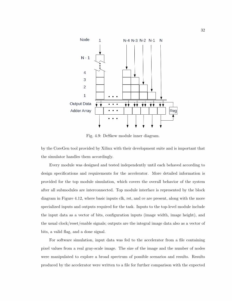
4.9 DeSkew module inner diagram. . . . . . . . . . . . . . . . . . . . . . . . . . 32
4.10 Main FSM for SAII controller module. . . . . . . . . . . . . . . . . . . . . . 33
4.11 Offset adjustment controller FSM. . . . . . . . . . . . . . . . . . . . . . . . 34
4.12 Block diagram of top model along with stimulus file read and write results. 35
4.13 Gray-scale portion of an image along with its pixel values and stimulus rep-resentation in bit-set form. . . . . . . . . . . . . . . . . . . . . . . . . . . . . 35
4.14 Hardware simulation flow showing input and output memory along withChipScope capturing results. . . . . . . . . . . . . . . . . . . . . . . . . . . 36

x
5.1 Speed-up obtained by the proposed SAII accelerator compared to the puresequential implementation. . . . . . . . . . . . . . . . . . . . . . . . . . . . 40
5.2 Visible overhead on the output of the SAII accelerator before first valid output. 41
5.3 SAII performance drop when image size decreases. . . . . . . . . . . . . . . 42
5.4 Detailed resource usage by individual modules in the SAII architecture. . . 43

xi
Acronyms
ASIC Application Specific Integrated Circuit
BRAM Block Random Access Memory
CLB Configurable Logic Block
CPU Central Processing Unit
DSP Digital Signal Processing
EDL Energy Dynamics Laboratory
FF Flip Flop
FPGA Field Programmable Gate Array
fps frames per second
FSM Finite State Machine
GPU Graphics Processing Unit
IOB Input Output Buffer
LUT Look Up Table
PAR Place And Route
PE Processing Element
RAM Random Access Memory
SA Systolic Array
SAII Systolic Array Integral Image
SM Switch Matrix
SURF Speeded-Up Robust Features
VHDL Very high speed integrated circuits Hardware Description Language
VLSI Very Large Scale Integration
1
Chapter 1
Introduction
1.1 Motivation
The ability to capture and analyze human behavior in real time has significant impact
on numerous applications such as gaming, retail shopping, high-fidelity lighting/HVAC
control, assisted living, and so on and so forth. The general area of computer vision has
seen rapid progress in several components of this broad research topic. Within this do-
main, the ability to reasonably assign the position of an occupant in a room via relative
distance/displacement with respect to objects of interest in real-time is a topic that is of
interest to the Intelligent Buildings group at Energy Dynamics Laboratory (EDL).
Accurately measuring an occupant’s position in a room has been a topic with a lot
of attention from the research community for many years and a lot of work related to the
topic can be found in journals and conference papers. Depth information is the key factor
when locating a person beyond the camera plane, depth allows for two-dimensional position
to be inferred, or at least estimated. The current depth estimation method used at EDL
is based on stereo cameras and a relative depth algorithm which makes use of Speeded-Up
Robust Features (SURF) [1] for disparity extraction across camera views. The first stage
of SURF involves the integral image calculation of the input video frame, making it a high
priority stage to avoid bottlenecks further on the process. The need for real-time integral
image calculation served as motivation for the design of an accelerator capable of providing
the parallelism required for critical image processing applications.
Since the time when Viola and Jones presented their work on rapid object detection [2],
the use of integral images has been the preferred way when computing features on an image
because of its noticeable reduction in computation time. Integral images use pre-calculated
integral values to achieve constant computation time independent of the size of the feature.
2
This provides a great speed improvement compared to the original and purely sequential
implementation, where all pixels had to be summed for every feature evaluation while sliding
the filter window across the image. Having the integral image available makes the feature
calculation a matter of just using four values to obtain the sum of pixels under any perimeter,
instead of constantly summing all pixels. The objective of this thesis is the optimization
of the integral image calculation step. With help of a scalable parallel approach, it is
possible to accelerate most image processing algorithms that make use of this approach.
The throughput of a system can be increased with help of a novel Systolic Array Integral
Image (SAII) accelerator, constrained only by memory bandwidth and resources available
on chip.
Many image processing algorithms make use of the integral image representation to
achieve near real-time execution speeds. Critical applications that expect low response
times generally require high frame-rate video inputs, typically in the order of 60 fps and
above. However, having hardware capable of processing video with such a throughput while
maintaining a small footprint and low power consumption is not a trivial task. This serves
as motivation for the Systolic Array (SA) inspired Integral Image accelerator proposed in
this thesis. The proposed design will provide a scalable approach capable of providing a
high level of parallelism.
1.2 Key Contributions
The main goal was to provide an accelerator capable of calculating multiple integral
pixels simultaneously while fully utilizing the memory bandwidth available. Some of the
distinguishable features of this architecture are listed below.
• The presented architecture has the advantage of being scalable, meaning that different
number of Processing Elements (PEs) can be used.
• The number of PEs can go from one up to the equivalent of the image width, as long
as the number of elements is an exact divisor of the image width.

3
• The number of PEs can be determined by the resources available or the speed required
for a particular application.
• The throughput of the accelerator is limited by the memory bandwidth supplying the
data to be processed.
• The architecture will compute multiple integral pixels every clock cycle; the number
of integral pixels generated will depend on the number of PEs.
• The overhead of the system to produce the first valid output is insignificant compared
to the size of the image.
• Processing speed is effectively divided by the number of PEs on the accelerator without
resulting in an increase of resources proportional to the number of PEs.
1.3 Thesis Overview
This thesis presents a hardware accelerator for integral image calculation by making
use of a systolic array approach. The document has been structured into six chapters for
better organization and understanding. In Chapter 1, a motivation is given as to why this
problem is of interest and why its application to a relative depth estimation algorithm is
currently under implementation. Also, a set of the most noticeable contributions produced
by this research are listed in this chapter. In Chapter 2, some background information
is given along with details on the relative depth estimation algorithm. Chapter 3 covers
integral image calculation basics and includes a literature review with contributions made
by other researchers working on the same area. Chapter 4 includes the implementation of
the hardware accelerator and simulation methods. Chapter 5 presents the results obtained
using the proposed accelerator architecture. Finally, Chapter 6 summarizes the conclusions
and future work ideas.
4
Chapter 2
Background
In this chapter background information is presented for a better understanding of the
proposed design and its implementation.
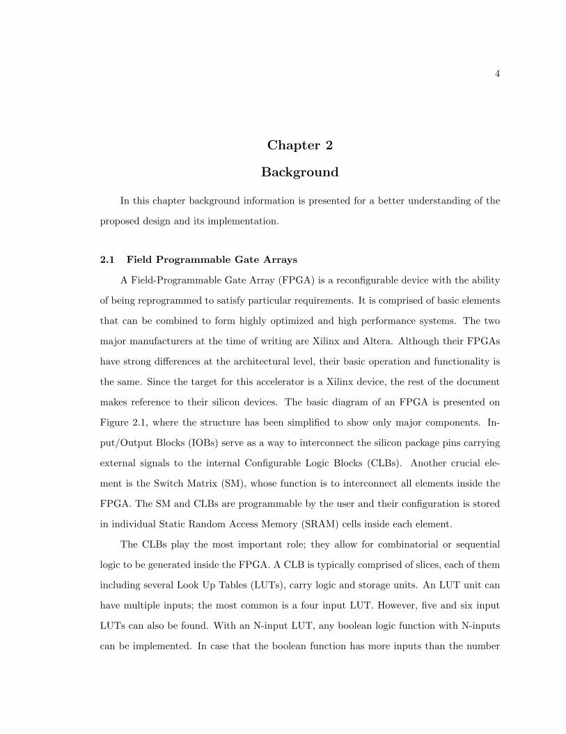
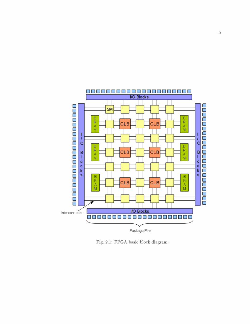
2.1 Field Programmable Gate Arrays
A Field-Programmable Gate Array (FPGA) is a reconfigurable device with the ability
of being reprogrammed to satisfy particular requirements. It is comprised of basic elements
that can be combined to form highly optimized and high performance systems. The two
major manufacturers at the time of writing are Xilinx and Altera. Although their FPGAs
have strong differences at the architectural level, their basic operation and functionality is
the same. Since the target for this accelerator is a Xilinx device, the rest of the document
makes reference to their silicon devices. The basic diagram of an FPGA is presented on
Figure 2.1, where the structure has been simplified to show only major components. In-
put/Output Blocks (IOBs) serve as a way to interconnect the silicon package pins carrying
external signals to the internal Configurable Logic Blocks (CLBs). Another crucial ele-
ment is the Switch Matrix (SM), whose function is to interconnect all elements inside the
FPGA. The SM and CLBs are programmable by the user and their configuration is stored
in individual Static Random Access Memory (SRAM) cells inside each element.
The CLBs play the most important role; they allow for combinatorial or sequential
logic to be generated inside the FPGA. A CLB is typically comprised of slices, each of them
including several Look Up Tables (LUTs), carry logic and storage units. An LUT unit can
have multiple inputs; the most common is a four input LUT. However, five and six input
LUTs can also be found. With an N-input LUT, any boolean logic function with N-inputs
can be implemented. In case that the boolean function has more inputs than the number
5
Fig. 2.1: FPGA basic block diagram.
6
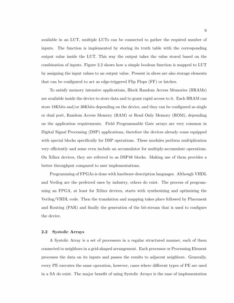
available in an LUT, multiple LUTs can be connected to gather the required number of
inputs. The function is implemented by storing its truth table with the corresponding
output value inside the LUT. This way the output takes the value stored based on the
combination of inputs. Figure 2.2 shows how a simple boolean function is mapped to LUT
by assigning the input values to an output value. Present in slices are also storage elements
that can be configured to act as edge-triggered Flip Flops (FF) or latches.
To satisfy memory intensive applications, Block Random Access Memories (BRAMs)
are available inside the device to store data and to grant rapid access to it. Each BRAM can
store 18Kbits and/or 36Kbits depending on the device, and they can be configured as single
or dual port, Random Access Memory (RAM) or Read Only Memory (ROM), depending
on the application requirements. Field Programmable Gate arrays are very common in
Digital Signal Processing (DSP) applications, therefore the devices already come equipped
with special blocks specifically for DSP operations. These modules perform multiplication
very efficiently and some even include an accumulator for multiply-accumulate operations.
On Xilinx devices, they are referred to as DSP48 blocks. Making use of them provides a
better throughput compared to user implementations.
Programming of FPGAs is done with hardware description languages. Although VHDL
and Verilog are the preferred ones by industry, others do exist. The process of program-
ming an FPGA, at least for Xilinx devices, starts with synthesizing and optimizing the
Verilog/VHDL code. Then the translation and mapping takes place followed by Placement
and Routing (PAR) and finally the generation of the bit-stream that is used to configure
the device.
2.2 Systolic Arrays
A Systolic Array is a set of processors in a regular structured manner, each of them
connected to neighbors in a grid-shaped arrangement. Each processor or Processing Element
processes the data on its inputs and passes the results to adjacent neighbors. Generally,
every PE executes the same operation, however, cases where different types of PE are used
in a SA do exist. The major benefit of using Systolic Arrays is the ease of implementation

7
Fig. 2.2: Mapping of a boolean function to an LUT.
on a VLSI chip, which comes from the regular structure of the arrays and the reuse of PE
blocks.
Systolic Arrays are a form of Single Instruction Multiple Data (SIMD) computers,
which can operate on multiple data with a single instruction. Data flow inside a systolic
array is highly parallelized and pipelined to achieve high throughputs. Every PE is assumed
to receive all required inputs simultaneously at the same clock edge, and the outputs are
ready in the subsequent cycle. The outputs of a Processing Element are the inputs to
neighbor PEs and should be transmitted synchronously.
Introduction of the SA in 1970 caused a great impact in general purpose computing
applications [3]. An important advantage of SAs is that the input has to be brought from
memory only once and can be used multiple times by the PEs. This is because PEs pass the
information between each other instead of going back to memory every time an operation
takes place. Kung [4] classified the SAs as semi-SAs and Pure-SAs depending on the way
data from memory is propagated to PEs. Semi-SAs are structures where a global data
communication is present on all PEs to deliver data requested from memory. In contrast,
Pure-SAs do not have a global data bus, and memory data enters the array through a single

8
PE and is propagated to other PEs every clock cycle until the last PE receives the data. A
visual representation of this advantage can be seen in Figure 2.3. Figure 2.3(a) shows how a
single PE would have to access memory for every iteration, while Figure 2.3(b) demonstrates
how the data from memory can be propagated to every node instead of generating a memory
access every time.
Since there was no widely accepted formal definition of Systolic Arrays, it was consid-
ered by Moreno and Lang to be a network of processing elements (PEs) with some basic
characteristics [5]:
• A linear or two-dimensional structure, comprised of nodes with up to four ports con-
nected with neighbors;
• External communication with Host is only possible from boundaries of the array;
• Communication between cells is uni-directional;
• No capability for broadcasting through cells without delay.
However, most of those characteristics have been modified. Currently it is possible to
find PEs with more than four inputs arranged in a three-dimensional structure. To save
resources, a uni-directional communication approach is not very attractive; a single PE’s
output can be fed back for reprocessing at expense of throughput while using less resources.
(a) Single Processing Element witha memory access in every executionloop.
(b) Multiple Processing Elements with singleaccess to memory.
Fig. 2.3: Comparison between a single PE and multiple PE in a systolic array structure.
9
Broadcasting can be of great benefit if the output data is needed by cells at the beginning of
the processing pipeline without additional delay. The integral image architecture proposed
in this thesis implements almost all these features, previously considered to violate the
definition of a SA, in order to achieve a nearly linear speed-up as a function of the number
of PEs used in the structure. Details on the characteristics of the proposed SA will be
presented in Chapter 4.
Memory inside PEs is another important topic; a typical systolic processing element
has no internal storage besides registers used to save input operands. Data flows through
the PEs on every clock cycle without saving any intermediate or previous results. Although
some applications require a storage element inside the nodes to save inter-node bandwidth,
usually the storage size is small and independent of the type of problem addressed by the SA.
This option becomes very handy when executing multiple operations with the input data and
stored data on a single clock cycle instead of having to require multiple inputs. Sometimes
cells have large storage elements; this helps further reduce the bandwidth between cells,
reduce the number of PEs required, or increase the number of operations per clock that a
PE can execute by reusing data.
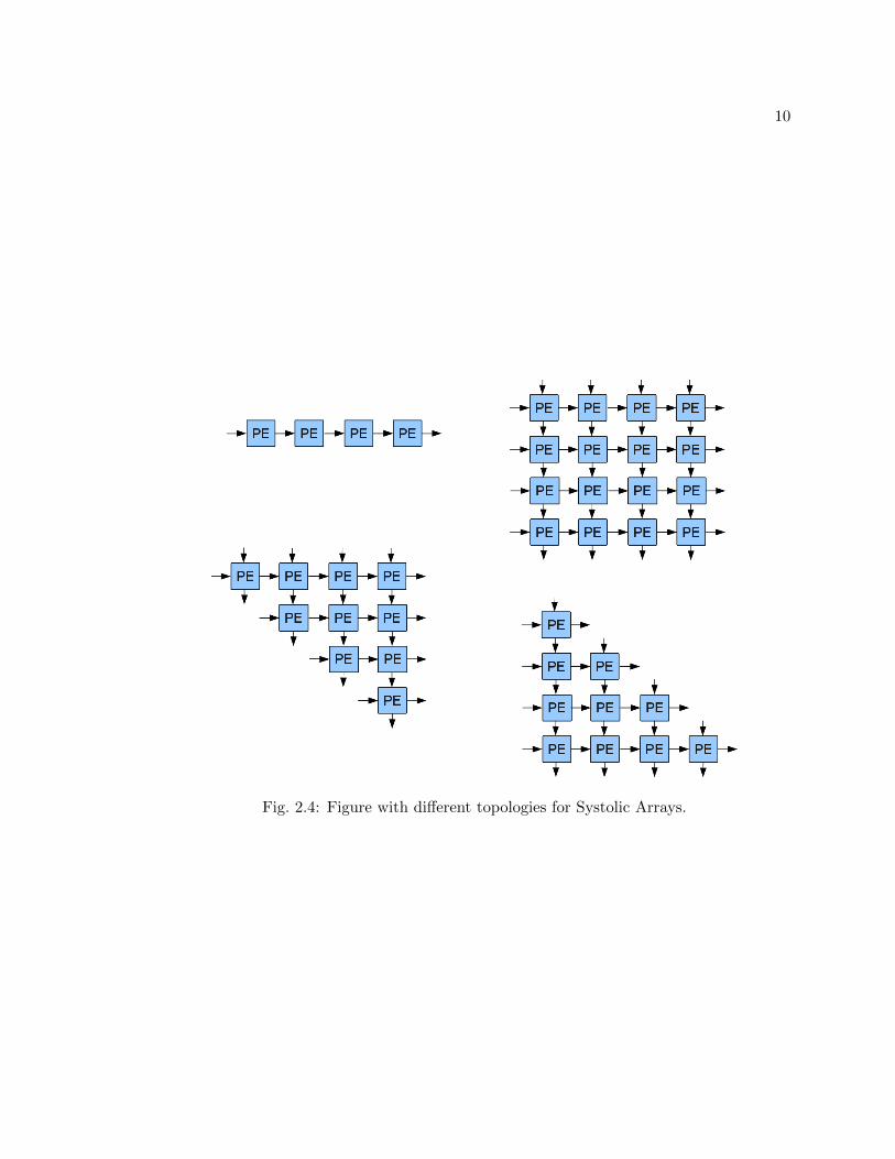
The type of PE is not the only variable when designing a Systolic Array; there are
also different topologies that can be implemented depending on the particular application.
Figure 2.4 has some of the possible topologies for SAs: rectangular, triangular, and linear.
The basic assumption with an SA is that data flows synchronously across the structure.
Each node is assumed to use its inputs and storage to generate an output and store the
result if needed in the future. However, in some cases the outputs are not generated on every
time step, making the design a pseudo-SA. In the implementation described in this thesis,
the PE has a significant amount of storage to reduce the number of nodes, allowing for a
simplified structure (one-dimensional) with the same throughput as a more complex two-
dimensional implementation. It has to be mentioned that the storage size is independent
of the number of PEs instantiated in the design. This is because the total storage required
to hold an image row is distributed equivalently between nodes.
10
Fig. 2.4: Figure with different topologies for Systolic Arrays.

11
Chapter 3
Integral Image
This chapter contains information related to integral image calculation and previous
work in this area.
3.1 Integral Image Calculation
Integral image representation of a gray-scale image allows for the sum of pixels inside a
region delimited by a rectangle with corners A, B, C, and D to be computed in constant time,
regardless of the size of the rectangle. Calculating the sum in constant time provides for a
noticeable speed-up when running box filters and calculating features. This is mainly due to
their dependence on the sum of pixel values underneath the variable size filter window while
it is displaced across the image. Each pixel in an integral image representation contains the
sum of all gray-scale pixels above and to the left as described by equation (3.1), making the
computation time dependent on the number of pixels in the image.
IΣ(x, y) =
i≤x∑i=0
j≤y∑j=0
I(i, j) (3.1)
Integral image representation only has to be calculated once and can be used many
times afterwards, this is of great advantage for algorithms requiring multiple computations
on the same image. Having the integral image representation available makes obtaining the
sum under a region of interest a process that only involves three arithmetic operations and
four data loads. Consider Figure 3.1 to be the integral image representation of an image
I, and A, B, C, and D the corners of a rectangle marking the boundary of the region of
interest, then the sum under the rectangle is calculated with SUM = D − B − C + A in
constant time.
12
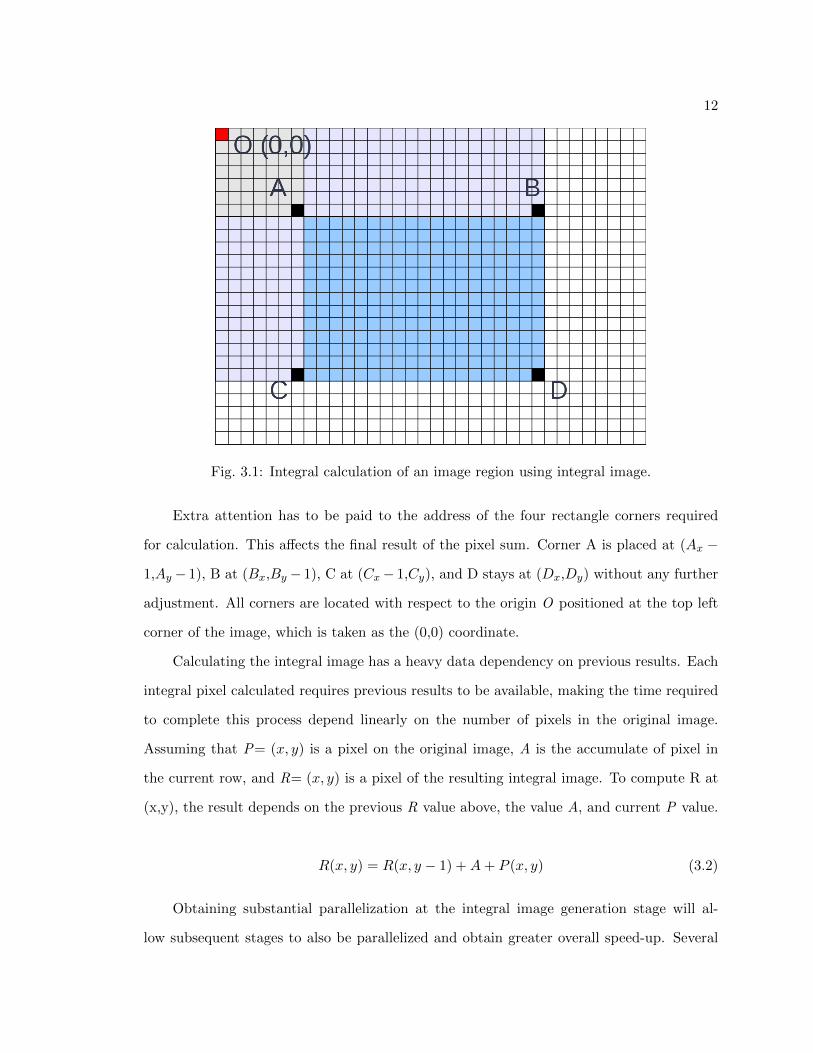
Fig. 3.1: Integral calculation of an image region using integral image.
Extra attention has to be paid to the address of the four rectangle corners required
for calculation. This affects the final result of the pixel sum. Corner A is placed at (Ax −
1,Ay − 1), B at (Bx,By − 1), C at (Cx− 1,Cy), and D stays at (Dx,Dy) without any further
adjustment. All corners are located with respect to the origin O positioned at the top left
corner of the image, which is taken as the (0,0) coordinate.
Calculating the integral image has a heavy data dependency on previous results. Each
integral pixel calculated requires previous results to be available, making the time required
to complete this process depend linearly on the number of pixels in the original image.
Assuming that P= (x, y) is a pixel on the original image, A is the accumulate of pixel in
the current row, and R= (x, y) is a pixel of the resulting integral image. To compute R at
(x,y), the result depends on the previous R value above, the value A, and current P value.
R(x, y) = R(x, y − 1) +A+ P (x, y) (3.2)
Obtaining substantial parallelization at the integral image generation stage will al-
low subsequent stages to also be parallelized and obtain greater overall speed-up. Several
13
approaches have been studied to efficiently make the integral image calculation parallel,
circumventing the data dependencies present in the purely sequential method.
3.2 Previous Work
The concept behind integral images is considered to be born with the work presented
by Crow [6] where the use of pre-calculated intensity tables was introduced. The tables
contained the sum of all the pixel intensities from any location on the table to the bottom left
corner, which was considered as the origin. Having this kind of table allowed for the average
of intensities to be found in constant time, regardless of size of the rectangle of interest.
This was specifically applied to make computational cost of texture-maps independent of
the texture density and to reduce computation cost.
The term integral image was not introduced until Viola and Jones [2] started using
an image representation that they applied to rapid object detection using boosted cascades
of simple features. Integral images allowed for Haar features to be evaluated faster and
in constant time. They achieved a speed-up of approximately 15 times compared to other
approaches by using gray-scale images and the integral image representation.
Many attempts have been made to optimize the performance of integral image com-
putation across a broad repertoire of systems and platforms. Messom and Barczak [7],
motivated by the importance of integral images and its use on many image processing algo-
rithms, took advantage of the stream processing capabilities of GPUs (Graphics Processing
Units) to improve its performance. The large number of processors on a GPU, compared
with the number of processors on a CPU (Central Processing Unit), was exploited to gain a
substantial increase in performance. Stream processing refers to the use of many processors
in a parallel implementation, where all of them work on a common task. This was used to
run a multi-pass prefix sum algorithm on all pixels in an image. The goal was to divide
the task into smaller tasks to reduce the total execution time of N log2N , where N is the
number of data elements to process and log2 is the number of passes required. By using
P number of processors, this is effectively reduced to N log2 NP , and achieving significant
improvement compared to a serial approach running on a CPU.
14
A more recent publication by Bilgic et al. [8] also targeted GPUs as a platform for
optimizing integral image computation. In this approach, the task of processing the integral
image was also delegated to the large quantity of processors in the Graphics Processing Unit
(GPU). The main idea behind this approach was to sum rows and columns independently.
Rows were first added and then the transpose of the results was obtained to process columns
using the same kernel. Images were divided into smaller blocks and distributed across thread
blocks on the GPU. The use of single precision floating-point computation has also been
evaluated, and achievements close to one order of magnitude improvement in speed are
claimed with respect to a sequential approach with a four mega-pixel image as input.
Terriberry et al. [9] introduced a novel approach based on Blelloch’s [10] approach and
extended it to compute multi-dimensional parallel prefix sums. The use of their novel two-
dimensional implementation and better cache handling, resulted in a 3.6 to 5.5 times speed
increase, and was used to accelerate SURF computation on GPU.
Other approaches focused on running the calculation on embedded systems with several
optimization techniques. Kisacanin [11] applied recursion and double buffering to the se-
quential implementation of the integral image calculation running on an embedded system.
The use of recursion allowed for the complexity of the algorithm to be reduced significantly,
and by using double buffering, data can be pulled from memory in to the first buffer while
the processor is working with data from the second buffer. Once the processing is done on
that buffer, the process can switch to the first buffer and start filling the second one. A
speed-up of five orders of magnitude is claimed using a 720 x 480 image size on a Texas
Instrument embedded media processor using this approach.
Multi-core implementations of the integral image computation have also been addressed
by several researchers. Zhang [12] studied the calculation of integral images in multi-core
processors by using a two-pass approach. First, rows are summed, and on a second pass
columns are summed in a parallel fashion, achieving double the speed of the best sequential
implementation. It has to be noted that one of the key contributions of this work was the
dependency of a chosen algorithm to the processor characteristics, e.g., bus speed, cache
15
effect, micro-architecture, and the topology of the processor.
Ehsan et al. [13] created a novel hardware algorithm capable of processing multiple
integral image rows in parallel. The main goal of this method was to save resources while
obtaining a significant increase in speed by starting multiple row processing in a cascaded
fashion. In theory they are able to compute four integral image pixels every clock cycle,
however, they had not yet implemented it in an FPGA at the moment of this publica-
tion. The results of using four simultaneous row processing on a 640 x 480 image can be
completed in 76800 clock cycles intead of the 307200 clock cycles required for a sequential
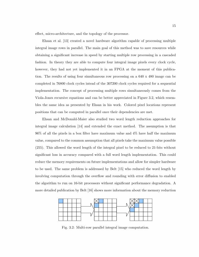
implementation. The concept of processing multiple rows simultaneously comes from the
Viola-Jones recursive equations and can be better appreciated in Figure 3.2, which resem-
bles the same idea as presented by Ehsan in his work. Colored pixel locations represent
positions that can be computed in parallel once their dependencies are met.
Ehsan and McDonald-Maier also studied two word length reduction approaches for
integral image calculation [14] and extended the exact method. The assumption is that
96% of all the pixels in a box filter have maximum value and 4% have half the maximum
value, compared to the common assumption that all pixels take the maximum value possible
(255). This allowed the word length of the integral pixel to be reduced to 21-bits without
significant loss in accuracy compared with a full word length implementation. This could
reduce the memory requirements on future implementations and allow for simpler hardware
to be used. The same problem is addressed by Belt [15] who reduced the word length by
involving computation through the overflow and rounding with error diffusion to enabled
the algorithm to run on 16-bit processors without significant performance degradation. A
more detailed publication by Belt [16] shows more information about the memory reduction
Fig. 3.2: Multi-row parallel integral image computation.
16
he achieved.
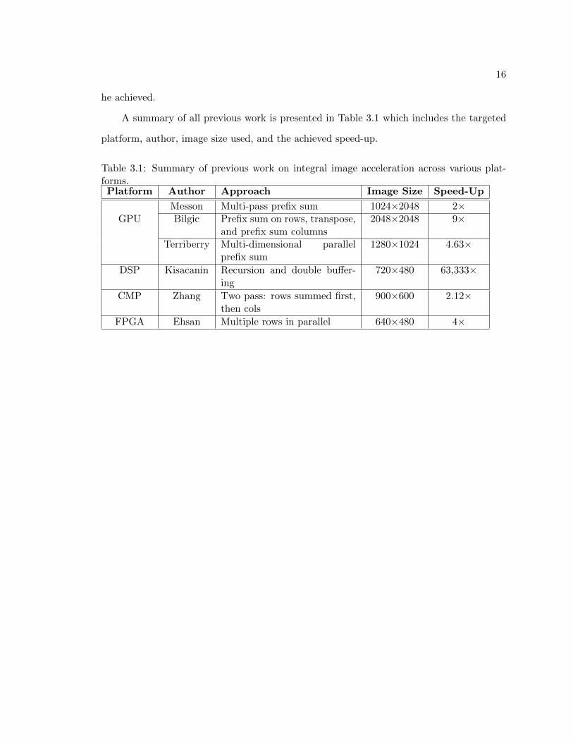
A summary of all previous work is presented in Table 3.1 which includes the targeted
platform, author, image size used, and the achieved speed-up.
Table 3.1: Summary of previous work on integral image acceleration across various plat-forms.Platform Author Approach Image Size Speed-Up
Messon Multi-pass prefix sum 1024×2048 2×GPU Bilgic Prefix sum on rows, transpose,
and prefix sum columns2048×2048 9×
Terriberry Multi-dimensional parallelprefix sum
1280×1024 4.63×
DSP Kisacanin Recursion and double buffer-ing
720×480 63,333×
CMP Zhang Two pass: rows summed first,then cols
900×600 2.12×
FPGA Ehsan Multiple rows in parallel 640×480 4×
17
Chapter 4
Implementation
The proposed accelerator architecture is designed to target Field Programmable Gate
Arrays (FPGAs) or an Application Specific Integrated Circuit (ASIC). The concept behind
the architecture was inspired by the effectiveness of Systolic Arrays and how they are able to
process large quantities of data synchronously every clock cycle. To ensure an optimal use
of memory accesses, it was chosen to process data coming from memory in row major order,
which is the way images are commonly stored, therefore requiring no additional memory
manipulation. The original design was based on a two-dimensional triangular Systolic Array
approach, and was later optimized to just require a one-dimensional structure. The final
architecture is structured as a linear Systolic Array that obtains the same speed-up and
reduces on-chip resources previously required for a two-dimensional implementation.
The goal of this accelerator is to produce multiple integral pixel results on the edge of
every clock cycle if valid data is available to process. An increased throughput on the integral
image stage, compared to the naıve or sequential implementation, allows for subsequent
stages that depend on the integral image results to also execute in parallel if designed with
that purpose in mind. More information on both approaches (two-dimensional and one-
dimensional), and details on the processing nodes are presented throughout this chapter.
4.1 Sequential Implementation
The most common approach to compute integral image is the sequential approach;
it can be found on many applications that require feature evaluation and filtering. The
sequential approach is a simpler architecture and can be coded in a shorter time compared
to a parallel approach. However, computing the integral image using the sequential approach
brings the disadvantage that it is only capable of producing one integral pixel every clock

18
cycle. If utilized on low speed video feeds or only used on sets of small images, then
the pure sequential implementation will suffice to supply the required throughput. For
applications that demand real-time execution this might not be enough, therefore requiring
other approaches like the one proposed in this thesis. Understanding this architecture will
help to understand the parallel architecture proposed in this thesis.
The architecture of the sequential approach can appreciated in Figure 4.1. The input
of the system is a single gray-scale pixel every clock cycle, which by definition is an 8-
bit number representing a range of intensities from 0-255. The block diagram describes
the operation and the flow of control and data signals used to produce an integral pixel
every clock cycle. The main components are: the integral image controller (IIG Controller),
previous row of integral image pixels (prev row), accumulator of gray-scale pixels on current
row (Acc), and two adders. The output is a single integral pixel, represented by a 32-bit
number, available every clock cycle assuming that input data is also available on every clock.
The main element is the controller, which keeps track of the original image size, syn-
chronization of signals and provides control signals to the rest of the system in the form of
last row (last row) and last column (last col) signals. As their names suggest, the former
becomes high when the last row of the original image is being processed and the latter
when the last column is reached. Both control signals in a high state indicate the end of
the image and that the integral image calculation is complete.
Input gray-scale pixel is summed with the content of an accumulator and is then added
with the integral pixel located above the current one to produce the integral pixel result.
The result from the first adder is further stored in the accumulator to be used on subsequent
cycles and the result from the second adder is used as a replacement for the previous row
pixel at the current index. Therefore, indexing the previous row provides the integral pixel
to be added and at the same time serves to store the result of given addition.
Control signals interact with the rest of the modules by reseting the accumulator once
the last column flag is set and the previous row array starts filling positions with zeros
instead of saving the integral pixel result when the last row flag is set high. Clearing the

19
Fig. 4.1: Pure sequential integral image implementation.
previous row to zero sets the conditions for the next image to start processing without
delays. It has to be noted that input pixels have to feed in row major order as stored in
memory, one row at a time going through all columns before passing to the next row.
4.2 Two-dimensional Systolic Array Accelerator
The first approach towards a parallel implementation of an integral image accelerator
was inspired by two-dimensional Systolic Arrays. A common SA structure is the rectangular
one, however for our purposes, the triangular one proved to be more appropriate based on
the way data has to flow and the operations involved in the computation of integral images.
With some analysis of the data and the way systolic arrays synchronously process data,
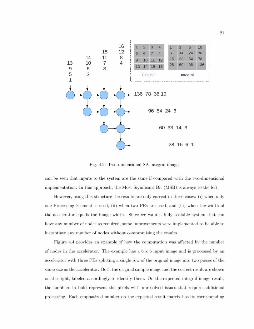
a two-dimensional implementation was designed. The architecture, as shown in Figure 4.2,
has two types of processing elements or nodes. The edge node is always the leftmost node
in the structure and only passes its results to the node on the right. The other type of node
is a regular Processing Element which takes an input from the top and the left, passing
results to the node on its right, and propagating the unaltered input to the one beneath.
By using a triangular structure, it is assured that memory is distributed across all nodes
and a node is only entitled to store a single previous integral pixel result before handing it

20
to its neighbors.
The sample image in Figure 4.2 is 4 x 4 pixels and is assumed to have pixel values from
1 - 16 for demonstration purposes only. It is appreciated how the data is placed on the
inputs at the top with a skew-like organization to ensure consistency and timing. Observe
that the inputs are to be placed in reverse order for the system to produce the correct
results. Outputs are also out of order; rows are actually the columns of the output integral
image representation, where the first element out of each row forms the first row of the
result, the second of each row belong to the second row and so on. Reorganizing the output
data is required to maintain addressing consistency along stages.
Data to the Systolic Array has to be provided in a synchronized manner to ensure that
data reaches the correct nodes at the right time to produce the correct result. Therefore,
data has to be skewed before passing it to the inputs of the Systolic Array. Skewing has to
be done in such a way that the first node to the left receives data first, and in the next clock
cycle its result has to reach the next node simultaneously with the corresponding input to be
processed together. The same propagation behavior happens along the complete structure.
4.3 One-dimensional Systolic Array Accelerator
After having designed the two-dimensional SA accelerator concept and simulated differ-
ent sizes of images, it was noticed that the same processing could be achieved with a fraction
of the resources previously used. This was achieved with the use of a one-dimensional sys-
tolic array approach capable of providing the same results with a L+12 % reduction in the
number of nodes required. Instead of using L2+L2 processing elements or nodes in the two-
dimensional architecture, it can be reduced to just L nodes (where L is the length of the
SAII accelerator). The reduction of nodes does not reduce the amount of inner memory
required by the system, therefore the resource savings are not linear with the number of
nodes eliminated. Memory actually depends on the width of the image to be processed,
this is because the previous row of integral results needs to be kept available to process the
rest of the image regardless of the number of PEs.
A representation of the one-dimensional SA implementation is shown in Figure 4.3. It
21
Fig. 4.2: Two-dimensional SA integral image.
can be seen that inputs to the system are the same if compared with the two-dimensional
implementation. In this approach, the Most Significant Bit (MSB) is always to the left.
However, using this structure the results are only correct in three cases: (i) when only
one Processing Element is used, (ii) when two PEs are used, and (iii) when the width of
the accelerator equals the image width. Since we want a fully scalable system that can
have any number of nodes as required, some improvements were implemented to be able to
instantiate any number of nodes without compromising the results.
Figure 4.4 provides an example of how the computation was affected by the number
of nodes in the accelerator. The example has a 6 x 6 input image and is processed by an
accelerator with three PEs splitting a single row of the original image into two pieces of the
same size as the accelerator. Both the original sample image and the correct result are shown
on the right, labeled accordingly to identify them. On the expected integral image result,
the numbers in bold represent the pixels with unresolved issues that require additional
processing. Each emphasized number on the expected result matrix has its corresponding

22
Fig. 4.3: One-dimensional SA implementation.
erroneous value marked on the output of the nodes. For example, {10, 15, 21} are the
expected values; however, {4, 9, 15} are the actual values produced by the nodes. The same
happens with the sets {44, 60, 78} and {14, 30, 48}. The second set needs to be normalized
with an offset of 30 and the first with 6. A trend was observed on the erroneous stream
of data produced, and it was noticed that erroneous sets were missing an offset value that
happens in the future. In the case of 4, 9, and 15, they all require the rightmost value
from the previous result row (6) to produce the correct set 4 + 6 = 10, 9 + 6 = 15, and
15 + 10 = 21. On the same figure, offsets have been identified with a bounding box; this
allows us to compare the time when this value is produced and the time step when it is
needed.
The offset value at the rightmost position of the output vector is separated from T0
by N − 1 clock cycles, where T0 is the time step when the value is expected to be available
and N is the number of PEs in the accelerator. To compensate for this problem, an extra
stage was added before outputs from the accelerator are final. Data coming out of the
PEs requires additional processing (DeSkew) such that data comes out aligned instead of

23
Fig. 4.4: Incorrect results when number of PEs /∈ {1, 2, image width}.
having a diagonal arrangement of data. When output data is aligned, the offset required to
normalize the current vector of results is only one clock cycle away, making this the optimum
point to correct the values produced before. The correction is achieved with a simple array
of 32-bit adders (one for each PE lane of results) and a single 32-bit accumulator to store
the previous row rightmost value. The only exception to this correction is when the current
vector of data is the first set of data of an integral row, as is shown in Figure 4.4; the first
elements of every row have the expected values and require no adjustment. It is not shown,
however, that exercising the node equations will demonstrate that the first set is always
correct regardless of the width of the accelerator. To account for this, the array of adders
at the end of the process will skip the beginning of every row of results to maintain the
consistency.
PEs are ruled by two different sets of equations listed in Table 4.1, which define the
results for each type of node in the accelerator.
As was mentioned before, the number of nodes can be adjusted to control the amount

24
Table 4.1: Set of equations for SAII accelerator PE nodes.Node Type Equations
Master NodeOutput = Inner mem(Index) + InputInner mem(Index) = Inner mem(Index) + InputFeed Out = Inner mem(Index) + Input
Helper NodeOutput = Inner mem(Index) Feed In + InputInner mem(Index) = Inner mem(Index) + InputFeed Out = Inner mem(Index) Feed In + Input
of resources dedicated to the accelerator, but the amount of memory required is constant for
the same size of the input image. equation (4.1) gives the amount of memory required per
node in the SA. More nodes in the system means that the inner memory will be smaller for
each node. The total memory depends on the input image width as described by equation
(4.2), where requirement is given in bytes assuming a 32-bit integral image result. Attempts
to reduce memory requirements exist [14, 16], and could bring this requirement down by
having a shorter integral pixel word length.
Node memory size =Image width
Number of PE∗ 4bytes (4.1)
Total memory size = Image width ∗ 4bytes (4.2)
With the proposed adjustments, the correct output is produced at all times at the cost
of an extra clock cycle without depending on the number of nodes in the SA structure. In
the next section the linear Systolic Array Integral Image (SAII) architecture is detailed as
a whole, including the control signals that arbiter the computation of the integral image,
ensuring the correct results are produced.
4.4 Integral Image Accelerator Architecture
Having a working Systolic Array architecture correctly processing data individually was
the first step; now it needs to be integrated into a system that a user would use and interact
with. The proposed core system will be in charge of arranging the input data, arbitrating

25
PE nodes, preparing results to be presented on the outputs, and adjusting results to obtain
the desired results. Having this level of abstraction is important to produce an efficient
interface for end users of this type of module. The simplified block diagram for the final
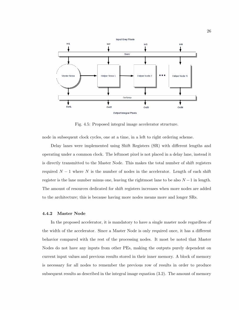
architecture is presented in Figure 4.5, where the different components can be appreciated.
The proposed architecture is composed of (i) a Skew block, where the input data is
arranged in the correct order for the PEs to process the data synchronously; (ii) a Master
Node; (iii) N − 1 Helper Nodes, where N is the number of nodes in the accelerator; and
(iv) a DeSkew block, which has to ensure that data produced by the nodes arrives to the
output in the correct order and also has to perform an offset adjustment before presenting
the results to the output of the accelerator.
Each component of the final architecture will be detailed separately in subsequent
sections of this chapter, including the controller which is not shown in the main block
diagram.
4.4.1 Skew - Data Preparation
Prior to any computation, it is of great importance that input data needing to be
processed arrives in the correct order to the processing nodes. This will ensure a synchronous
and correct operation. If input data was to arrive with wrong timing, the result would not
be reliable and subsequent results would also be affected.
To ensure that data is always delivered to the PEs synchronously, a Skew module was
designed to properly arrange input data without having the host system worry about input
data ordering to use this integral image accelerator. Input data vector contains multiple
gray-scale pixel values; each of them needs to be delayed differently such that when the
rightmost pixel is processed by its corresponding processing node, the result of all previous
pixels are already available for it to use. A graphical representation of this skewed delay
method can be appreciated in Figure 4.6. Input data, as labeled in the aforementioned
figure, can have N pixels, and each one is placed in a delay lane with increasing length up
to N − 1. The leftmost pixel is passed to the Master Node without further delay to start
the processing sequence. The rest of the pixels will arrive at their corresponding processing
26
Fig. 4.5: Proposed integral image accelerator structure.
node in subsequent clock cycles, one at a time, in a left to right ordering scheme.
Delay lanes were implemented using Shift Registers (SR) with different lengths and
operating under a common clock. The leftmost pixel is not placed in a delay lane, instead it
is directly transmitted to the Master Node. This makes the total number of shift registers
required N − 1 where N is the number of nodes in the accelerator. Length of each shift
register is the lane number minus one, leaving the rightmost lane to be also N −1 in length.
The amount of resources dedicated for shift registers increases when more nodes are added
to the architecture; this is because having more nodes means more and longer SRs.
4.4.2 Master Node
In the proposed accelerator, it is mandatory to have a single master node regardless of
the width of the accelerator. Since a Master Node is only required once, it has a different
behavior compared with the rest of the processing nodes. It most be noted that Master
Nodes do not have any inputs from other PEs, making the outputs purely dependent on
current input values and previous results stored in their inner memory. A block of memory
is necessary for all nodes to remember the previous row of results in order to produce
subsequent results as described in the integral image equation (3.2). The amount of memory

27
Fig. 4.6: Skew module inner diagram.
required is ImagewidthNumberofNodes and it only holds results generated by itself. Lets assume that
the input image has a width of 24 pixels and the accelerator has four processing nodes; this
leaves every node holding 244 = 6 integral pixels. With a memory size of six integral pixels
(32-bits), the Master Node would hold integral pixel results at positions 1, 5, 9, 13, 17, 21.
The behavior of this node is described by the set of equations (4.3), (4.4), and (4.5).
Output = Inner mem(Index) + Input (4.3)
Inner mem(Index) = Inner mem(Index) + Input (4.4)
Feed Out = Inner mem(Index) + Input (4.5)
A visual representation of a Master Node is given in Figure 4.7, where all interface ports
and basic inner component representations can be appreciated for a better understanding of
the implementation. The node has the typical clk, rst, and ce signals to maintain synchro-
nization with the rest of the system. Besides that, it has an 8-bit input port and a done flag,
which tells the Node to clear its memory and outputs in preparation for a new image frame

28
Fig. 4.7: Master node inner diagram.
once the current image has finished processing. On the outputs, it has a 32-bit output and
feed out signals, along with a single valid bit that indicates when a valid value is produced
by the node. The abstract representation includes some components that help visualize
the operations the node undertakes. It has two 32-bit adders and a 32-bit memory block
holding previous results as mentioned before. The multiplexer activated by the Done signal
allows for the system to start filling the SA with zeros to avoid perturbing the calculations
in other nodes.
The naming of both types of nodes comes from the first stages of the design when the
Master Node had additional logic that made it more complex. Names stayed unaltered when
the Master Node was simplified and the data offset adjustment was moved to a posterior
stage of the processing pipeline. The change was due to an inconsistency and incapacity of
the system to compute the integral image with accelerator sizes other than 1, 2, and N.

29
4.4.3 Helper Node
The accelerator is composed of two types of processing nodes. Since only one Master
Node is allowed in the proposed design, the rest of the processing power is provided by
multiple Helper Nodes. There can be any number of Helper Nodes in the design to expand
the accelerator, the only constraint is that there must always be a total number of PEs that
exactly divide the width of the image.
A Helper Node is ruled by a different set of equations than the Master Node because
of its additional input from neighbor nodes. The set of equations (4.6), (4.7), and (4.8)
describe how the outputs and inputs interact to generate the pre-integral pixels. Just as
a reminder to the reader, the output from the PEs need further offset adjustment before
representing the actual integral image.
Output = Inner mem(Index)Feed In+ Input (4.6)
Inner mem(Index) = Inner mem(Index) + Input (4.7)
Feed Out = Inner mem(Index)Feed In+ Input (4.8)
By observing Figure 4.8, the reader could be under the impression that a Helper Node
takes less resources than a Master Node, but is actually the opposite, as it has more inputs
to process. Having an additional input automatically instantiates a three input 32-bit adder
instead of a two input one like in the case of a Master Node. The rest of the components
are considered to be the same, including the inner memory block, which is the same size on
all nodes of an accelerator.
4.4.4 DeSkew - Data Normalization
This module does the opposite of the Skew; it removes the skewed look of the data
coming out of the nodes. It also has the task of adjusting the offset of the data going out

30
Fig. 4.8: Helper node inner diagram.
of the accelerator. The operation is split in two phases; the one that will ensure that the
output of each PE is placed in its corresponding delay lane. The other, which is the offset
adjustment, was accomplished with aid of an array of adders and a 32-bit accumulator which
stores the previous rightmost output for subsequent additions. Figure 4.9 tries to throw
more light on this, to help us understand the final adjustment and the correctly ordered
results.
The reordering of results is achieved in the same manner as the input data was prepared
for the nodes to process with help of a different length shift register in each lane to serve
as a controlled delay. Shift registers are ordered in decrementing length from left to right,
and the rightmost has no delay at all. After the values have been restored to proper order,
the data is handed to an offset adjustment module that will add the missing offset to each
set of data. Offset is taken from the rightmost value of each data set generated by the
DeSkew stage and stored in a local register to use on the next iteration. The local register
has a storage capacity of 32-bits, assuming that the integral pixel is that size, but it can be
reduced if a word length reduction method is used on the integral pixel.

31
Offset adjustments consist of adding the local register value to all the elements in the
output data set and refreshing the value of the register with the most recent result produced.
The operation is applied to all outputs with the exception of the first element of each image
row which does not need adjustment. Arbitration of the outputs that require adjustment
is managed by the controller who emits a bypass signal indicating that the current data
requires no further adjustment. The system skips the addition when it sees the bypass flag;
however, it does refresh the local register value for future use.
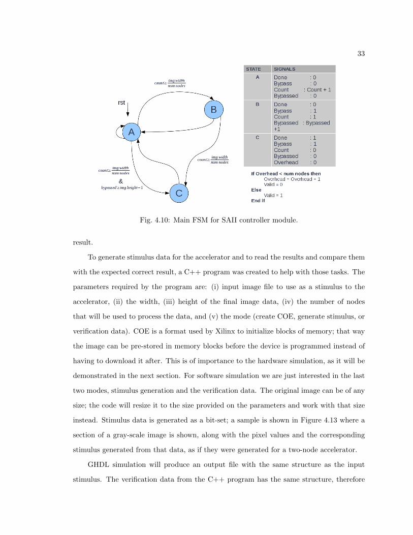
4.4.5 Controller
This is the module that carries the burden of synchronizing the accelerator by using a
set of control signals at the appropriate time. The easiest way to explain this controller is
to show the Finite State Machine (FSM) diagrams involved in the system behavior. The
FSM diagram is presented in Figure 4.10, where all states and their transition conditions
are displayed along with the state of control signals.
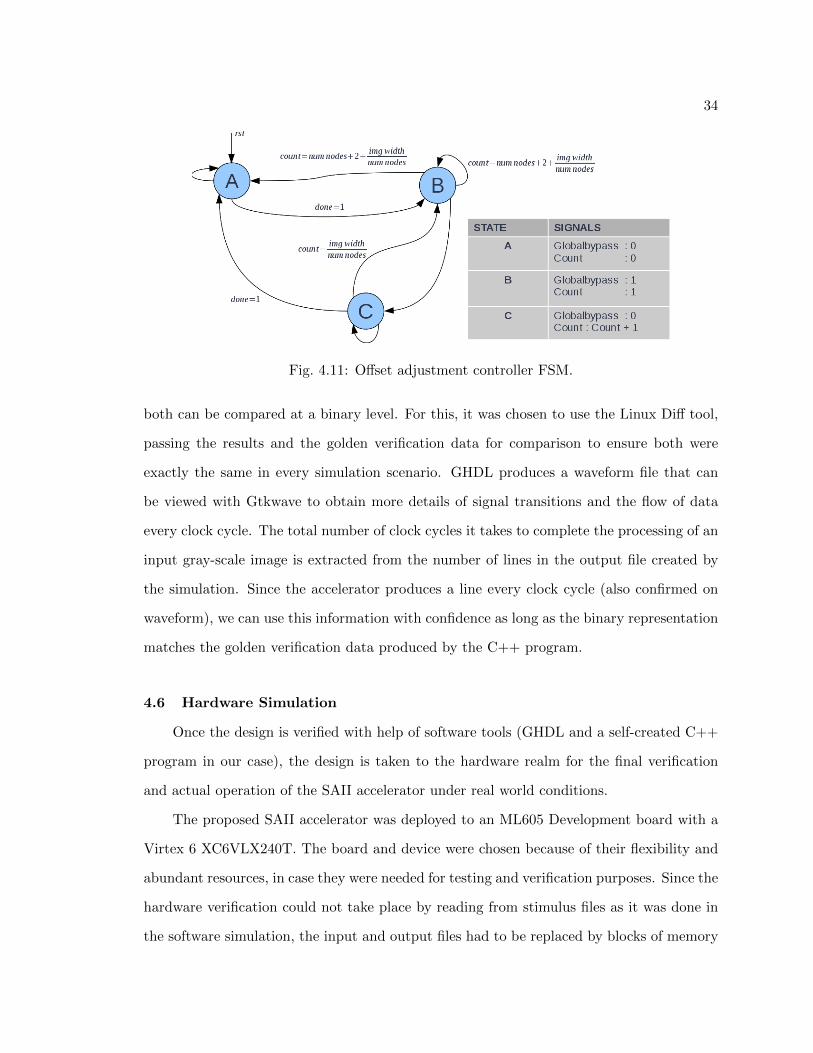
There is also the requirement to control the offset adjustment module to skip the
addition of the register value to the first set of data of each integral image row. The FSM
that generates the globalbypass signal, as it is called, is described in Figure 4.11.
4.5 Software Simulation
Verification of the design was first completed using a software simulator, and once it
was confirmed that all parts of the design worked as expected, the design was implemented
on a Virtex 6 device to ensure actual hardware acceleration beyond software simulations.
The simulation software used for verification was GHDL, which is an open source
tool developed and maintained by Tristan Gingold [17]. This tool is perfectly capable of
simulating complex designs in VHDL language, even if Xilinx Libraries and Primitives are
used in the design. However, advanced knowledge and skills are required to setup and use
the mentioned libraries due to the fact that it is an open source and Xilinx libraries are
proprietary. The SAII accelerator proposed in this thesis makes use of some generated cores
32
Fig. 4.9: DeSkew module inner diagram.
by the CoreGen tool provided by Xilinx with their development suite and is important that
the simulator handles them accordingly.
Every module was designed and tested independently until each behaved according to
design specifications and requirements for the accelerator. More detailed information is
provided for the top module simulation, which covers the overall behavior of the system
after all submodules are interconnected. Top module interface is represented by the block
diagram in Figure 4.12, where basic inputs clk, rst, and ce are present, along with the more
specialized inputs and outputs required for the task. Inputs to the top-level module include
the input data as a vector of bits, configuration inputs (image width, image height), and
the usual clock/reset/enable signals; outputs are the integral image data also as a vector of
bits, a valid flag, and a done signal.
For software simulation, input data was fed to the accelerator from a file containing
pixel values from a real gray-scale image. The size of the image and the number of nodes
were manipulated to explore a broad spectrum of possible scenarios and results. Results
produced by the accelerator were written to a file for further comparison with the expected
33
Fig. 4.10: Main FSM for SAII controller module.
result.
To generate stimulus data for the accelerator and to read the results and compare them
with the expected correct result, a C++ program was created to help with those tasks. The
parameters required by the program are: (i) input image file to use as a stimulus to the
accelerator, (ii) the width, (iii) height of the final image data, (iv) the number of nodes
that will be used to process the data, and (v) the mode (create COE, generate stimulus, or
verification data). COE is a format used by Xilinx to initialize blocks of memory; that way
the image can be pre-stored in memory blocks before the device is programmed instead of
having to download it after. This is of importance to the hardware simulation, as it will be
demonstrated in the next section. For software simulation we are just interested in the last
two modes, stimulus generation and the verification data. The original image can be of any
size; the code will resize it to the size provided on the parameters and work with that size
instead. Stimulus data is generated as a bit-set; a sample is shown in Figure 4.13 where a
section of a gray-scale image is shown, along with the pixel values and the corresponding
stimulus generated from that data, as if they were generated for a two-node accelerator.
GHDL simulation will produce an output file with the same structure as the input
stimulus. The verification data from the C++ program has the same structure, therefore
34
Fig. 4.11: Offset adjustment controller FSM.
both can be compared at a binary level. For this, it was chosen to use the Linux Diff tool,
passing the results and the golden verification data for comparison to ensure both were
exactly the same in every simulation scenario. GHDL produces a waveform file that can
be viewed with Gtkwave to obtain more details of signal transitions and the flow of data
every clock cycle. The total number of clock cycles it takes to complete the processing of an
input gray-scale image is extracted from the number of lines in the output file created by
the simulation. Since the accelerator produces a line every clock cycle (also confirmed on
waveform), we can use this information with confidence as long as the binary representation
matches the golden verification data produced by the C++ program.
4.6 Hardware Simulation
Once the design is verified with help of software tools (GHDL and a self-created C++
program in our case), the design is taken to the hardware realm for the final verification
and actual operation of the SAII accelerator under real world conditions.
The proposed SAII accelerator was deployed to an ML605 Development board with a
Virtex 6 XC6VLX240T. The board and device were chosen because of their flexibility and
abundant resources, in case they were needed for testing and verification purposes. Since the
hardware verification could not take place by reading from stimulus files as it was done in
the software simulation, the input and output files had to be replaced by blocks of memory

35
Fig. 4.12: Block diagram of top model along with stimulus file read and write results.
Fig. 4.13: Gray-scale portion of an image along with its pixel values and stimulus represen-tation in bit-set form.
instantiated using BRAMS in the FPGA as shown in Figure 4.14. Additional memory
addressing modules were added to control the loads and stores to outer memory blocks
containing the original image and to store the results. Since the focus of this thesis is a
novel integral image accelerator, memory interfaces are not of interest and are not discussed
in this document. Due to the lack of an interface to fill memory with the original image from
outside the FPGA, it was chosen to have memory pre-initialized with the image data before
programming the device. Our C++ program has the ability to take the original image file
on the host computer and produce a COE compliant file that serves as initialization data

36
for the block of memory generated with Xilinx CoreGen.
The results from the accelerator are stored in an output memory block comprised of
multiple Brams. However, reading that output memory is not possible without additional
interface to the host computer. Therefore, Chipscope was used instead to monitor the
output of the accelerator and other critical signals that reflect the status of the accelerator.
Chipscope is a tool similar to common logic analyzers; however, it currently has a key
benefit of being able to debug signals that have no physical connection. Since Chipscope is
a module sitting in the inside of the FPGA, it can capture signals that otherwise would be
impossible to reach from outside the chip.
Information captured by Chipscope is of great value when looking for timing issues
and verifying correct execution of the inner modules of the design. Data can be represented
in many formats and plotted in waveform style for a more efficient inspection and better
readability.
Fig. 4.14: Hardware simulation flow showing input and output memory along with Chip-Scope capturing results.

37
Chapter 5
Results
This chapter presents the results of the proposed Systolic Array Integral Image (SAII)
accelerator and comparisons with the purely sequential approach as described in Chapter 3.
Based on the fact that the parallel approach by Ehsan et al. [13] to accelerate integral image
computation as described in their publication was not implemented in hardware, it can
not be compared beyond the number of clock cycles required to complete the calculation.
The proposed design is instead compared with the sequential approach running on the
same FPGA device as the proposed SAII accelerator. Comparison between approaches
considers the number of clock cycles required to process the input image and the maximum
frequency achieved by each design after Place and Route (PAR). From those two values, the
processing speed is estimated. This is because the purely sequential approach has a different
clock frequency than the proposed design due to differences in the design complexity. The
difference in clock frequency across implementations affects the outcome of the comparison.
The proposed design will only be compared with the sequential approach as they are
the only implementations that share a common target platform (FPGA). However, fps can
be easily calculated using the equations provided in this chapter to compare with other
platforms. The proposed accelerator was not compared with other target platforms besides
FPGAs because of their differences in footprint, power consumption, and other factors that
defeat the purpose of having an embedded image processing solution.
The SAII accelerator was implemented in VHDL and synthesized using Xilinx ISE 12.1.
The specific target platform for comparisons is a Virtex 6 LX240T FPGA.
5.1 Execution Time
Verification of the design took place with different image sizes (1280x960, 640x480,

38
320x240, 160x120, 80x60, and 40x30 pixels) and a subset of all the possible number of PEs
that the SAII accelerator can have (2, 4, 8, 16, 32 nodes). Various combinations of these
parameters were made to analyze the performance of the proposed integral image accelerator
under several scenarios. It is already known from Chapter 4 that the purely sequential
implementation of an integral image architecture is capable of processing a single gray-scale
pixel every clock cycle. Therefore, the total execution time in clock cycles can be calculated
with (ImageWidth) ∗ (ImageHeight) for the sequential implementation. Conversion from
total clock cycles to execution time was required to fairly compare the sequential approach
and the different sizes of the proposed design (differences exist in the maximum frequency
achievable by each approach). Execution times for the sequential and the proposed SAII
architecture are listed in Table 5.1 for comparison purposes. It can be seen that execution
time (in microseconds) of the proposed design is lower on all test cases and for all sizes
of the SAII accelerator being the difference more pronounced at larger number of PEs as
expected.
5.2 Speed-Up
Based on the execution time previously presented, speed-up of the proposed acceler-
ator compared with the sequential approach under different scenarios is shown in Figure
5.1. Speed-up is obtained by using the execution time of the sequential implementation as
reference. Results not plotted correspond to test scenarios where the input image width
Table 5.1: Total execution time estimate for the sequential implementation and varioussizes of the SAII accelerator. Time estimate based on total clock cycles required to processan image and the maximum clock frequency achievable after synthesis.
Execution Time (µs)
Approach\Image Size 1280x960 640x480 320x240 160x120 80x60 40x30
SequentialCPU 15361 4570 1652 239 117 49
SequentialFPGA 8610.167 2152.542 538.135 134.534 33.633 8.408
2 PEs 4331.554 1082.915 270.755 67.715 16.955 4.265
4 PEs 2132.345 533.123 133.317 33.366 8.378 2.131
8 PEs 1066.225 266.613 66.711 16.735 4.241 1.118
16 PEs 533.206 133.400 33.449 8.461 2.214 NA
32 PEs 266.780 66.877 16.902 4.408 NA NA

39
was not exactly divisible by the number of nodes in the accelerator.
Figure 5.1 includes a range of image sizes used for the design verification where each
integral image was calculated with different numbers of processing elements in the SAII
accelerator. It can be appreciated that by using the SAII approach, an average speedup
between 1.987 - 32.27X is obtained, depending on the number of processing elements used
(2 - 32, respectively). Under some conditions, the proposed accelerator achieves a speed-up
greater than the number of PEs used because of the higher operational frequency it achieves
over the sequential implementation.
The number of PEs can be increased to further demonstrate the speedup that can be
obtained with the proposed accelerator; however, performance is susceptible to a constant
overhead delay that depends on the number of PEs in the accelerator. Figure 5.2 shows
how the measured overhead is constant for the same number of PEs across all image sizes.
Overhead is dependent on the number of nodes in the accelerator, the time it takes to
propagate input data from the first node to the last one, and the time it takes to produce
the first valid data on the output.
Because of the aforementioned constant overhead for each accelerator size, performance
drops when the image width gets closer in size to the overhead value. An example can be
observed in Figure 5.3, where an 8 PE accelerator (with an overhead of 11 clock cycles)
starts losing performance when the size of the input image starts decreasing, making itself
more pronounced as the size approaches 40 x 30 pixels. Small images are frequently used in
image processing when working with reduced regions of interest; therefore, it is important
to achieve an acceptable speed-up across a wide range of image sizes, including smaller
ones. Although performance shows a slight drop with smaller images, the speed-up is
still several times higher than with the sequential implementation. Even compared with
Ehsan’s approach, where a 4X speed-up is claimed prior to implementation in hardware,
almost 8 times more speed-up than Ehsan’s approach is obtained by using the proposed
SAII accelerator with 32 PEs when processing small images.

40
Fig. 5.1: Speed-up obtained by the proposed SAII accelerator compared to the pure sequen-tial implementation.
5.3 Resources
Resource utilization was quantized for each SAII accelerator size and is presented in
Table 5.2 for further analysis. Included in that table are the number of Look Up Tables
(LUTs) and Flip Flops (FFs) used by sequential implementation, as well as different sizes
of the proposed architecture. Additionally, the maximum frequency that each design can
achieve was extracted from ISE to fairly compare both approaches. As the number of PEs
in the proposed architecture increases, the number of FF also increases. LUT utilization
has a different behavior; as the number of PEs increases, the number of LUTs used drops
until it reaches eight nodes, then it increases afterwards. This behavior might be due
to the effectiveness of PAR tools and the efficient filling of FPGA slices when using key
accelerator sizes. The maximum frequency that each design can achieve shows that the
proposed architecture is capable of achieving higher operational frequencies compared to
the sequential approach on all accelerator sizes, except with two nodes.
To further understand the resource utilization of the proposed accelerator, every module

41
Fig. 5.2: Visible overhead on the output of the SAII accelerator before first valid output.
Table 5.2: FPGA resources utilized by the sequential approach and the proposed SAII withdifferent number of PEs.
Implementation
Resources Sequential 2 4 8 16 32
FFs 42047 41401 41710 42261 43397 45653
LUTs 34289 45573 41363 34201 39638 40783
Max. Freq. (Mhz) 142.715 141.844 144.07 144.07 144.07 144.07
was analyzed independently. It was observed in Table 5.2 that the LUT utilization was
decreasing as the number of nodes increased. Having individual resource measurements
allowed for trends to be extracted based on the number of PEs in the accelerator. Results
are presented in Figure 5.4 for all major modules of the SAII accelerator. From the obtained
trends several facts can be deduced: (i) Since arithmetic inside both processing elements
(PEs) is constant regardless of the size of the accelerator, the reduction of resources is only
due to the reduction of inner storage as it becomes distributed across more nodes; (ii) The
controller is completely independent of the accelerator size; (iii) Skew and DeSkew resources
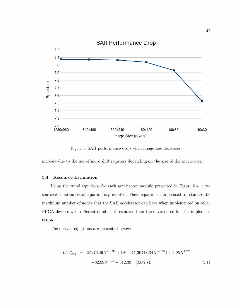
42
Fig. 5.3: SAII performance drop when image size decreases.
increase due to the use of more shift registers depending on the size of the accelerator.
5.4 Resource Estimation
Using the trend equations for each accelerator module presented in Figure 5.4, a re-
source estimation set of equation is presented. These equations can be used to estimate the
maximum number of nodes that the SAII accelerator can have when implemented on other
FPGA devices with different number of resources than the device used for this implemen-
tation.
The derived equations are presented below:
LUTreq = 55276.49N−0.99 + (N − 1)(30478.34N−0.94) + 3.95N1.22
+82.99N1.05 + 512.39 (LUTs), (5.1)

43
(a) Skew module resource utilization and estimation equation.
(b) Master Node resource utilization and estimation equation.
(c) Helper Node resource utilization and estimation equation.
(d) DeSkew module resource utilization and estimation equation.
(e) Controller resource utilization and estimation equation.
Fig. 5.4: Detailed resource usage by individual modules in the SAII architecture.

44
FFreq = 40970.19N−0.99 + (N − 1)(40809.12N−0.98) + 3.95N1.22
+64N1 + 181 (FFs), (5.2)
NumberOfNodesaprox =LUTavail − 55875.33
102.28, (5.3)
NumberOfNodesaprox =FFavail − 41219.14
102.23. (5.4)
Using this estimation method, Table 5.3 is presented as an example of how the SAII
would look on different FPGA devices. The calculations were made under the assumption
that all resources are devoted to the accelerator, which rarely will be the case in a real-world
application. However, resources used for estimation can be the ones available for integral
image purposes when other designs are also to be placed in the same device.
5.5 SAII Accelerator Model
Based on results and design characteristics, a model of the proposed SAII accelerator
was extracted. Using the given set of equations, it is possible to extrapolate the design
Table 5.3: Maximum number of PE nodes that can be instantiated across several devices.Negative estimations refer to non-capable devices. The minimum of LUT and FF nodesestimates is considered.
FFs Nodes LUTs Nodes Estimated Nodes
Spartan 3 XC3S1600E 29,504 -69 29,504 -138 -138
Spartan 6 XC6SLX100 126,576 503 63,288 39 39
Spartan 6 XC6SLX150 184,304 843 92,152 190 190
Virtex 4 XC4VLX40 53,248 71 106,496 266 71
Virtex 4 XC4VLX200 178,176 806 356,352 1577 806
Virtex 6 XC6VLX130T 160,000 699 80,000 127 127
Virtex 6 XC6VLX240T 301,440 1532 150,720 498 498
Virtex 6 XC6VLX760 948,480 5342 474,240 2196 2196
Artix 7 XC7A105 129,600 520 64,800 47 47
Artix 7 XC7A335T 440,400 2351 220,200 862 862

45
to other devices that might have different resource counts, different clock frequencies, or
just another performance requirement. MaxFrequencySAII is the maximum frequency at
which the accelerator can run on a particular device. Overhead is the number of clock cycles
required until the first valid data is presented to the output. The rest of the parameters
should have names clearly related to their meaning, and should not cause confusion.
Overhead = NumberOfNodes+ 3 (cycles) (5.5)
TimeSAII =Cyclestotal
MaxFrequencySAII(seconds) (5.6)
Cyclestotal = Overhead+
[ImageWidth
NumberOfNodes∗ ImageHeight
](cycles) (5.7)
Speedup =
(ImageWidth∗ImageHeight)MaxFrequencyseq
TimeSAII(X) (5.8)
fps = (TimeSAII)−1 (fps) (5.9)
NumberOfNodesaprox =Cyclestotal
ImageWidth ∗ ImageHeight
−1
(elements) (5.10)
46
Chapter 6
Conclusions and Future Work
This chapter contains the conclusions obtained from simulation results of the proposed
architecture and some future work for upcoming research opportunities.
6.1 Summary
A novel scalable integral image accelerator was proposed based on systolic array ar-
chitectures. Simulations that involved multiple input image sizes and different number of
nodes in the accelerator were used to validate the design. The SAII accelerator is capable
of achieving a speed-up that depends almost linearly on the number of processing elements
instantiated in the architecture having as a limit the availability of resources. Based on the
results, an average speed-up of 1.98X 32.27X was obtained by the proposed architecture
over the basic sequential approach when using 2 - 32 PEs in the SAII accelerator.
The system offers scalability by allowing for the number of processing elements in the
accelerator to be adjusted as needed. Speed-up is dependent on the number of nodes on the
system, assuming that there is enough memory bandwidth to feed all processing nodes with
data every clock cycle and resources to instantiate them. In some cases memory bandwidth
is not a constraint. For example, images can be entirely downloaded to inner memory blocks
and then processing can begin with a larger number of PEs. This is very similar to what
a GPU approach does, where the host computer transfers the input image to the GPU’s
shared memory and then processes it, and writes it back.
A set of parameterized equations were derived to model the proposed architecture
under various scenarios. The model was parameterized with respect to the size of the input
image (width and height), total clock cycles, frames per second, desired speed-up, number
of Processing Elements (PE), and overhead to first valid data.
47
By using those equations, it is possible to estimate the maximum speed-up obtainable
on FPGAs with different amounts of resources available. A sample of such a projection was
shown on previous chapter.
6.2 Future Work
The accelerator proposed in this thesis was designed static in nature and is only viable
for known maximum image sizes prior to implementation, as the number of nodes cannot be
changed during runtime. Having a static implementation means additional work is needed
to determine the optimal number of nodes that can solve all the cases while satisfying
the resource constrains established by the design requirements. Extra functionality can be
obtained from this design if the accelerator is converted into a dynamic implementation,
meaning that the system could adapt the number of nodes to the conditions of a particular
task or field application dynamically.
A dynamic implementation would not affect resource utilization, but it would require
restructuring memory locations and control signals. In order to make such an approach
viable, it would be required that the disabled nodes resources be used for other tasks (for
example, Box Filtering) when they were not in use for integral image calculation. This could
be done by either having polymorphic nodes or by using Partial Dynamic Reconfiguration
(PDR). By using polymorphic nodes, nodes can be instructed to do different tasks while
keeping all their inherent functionalities, just using the fraction intended for the active task.
Using PDR has its advantages and disadvantages. No resources are wasted by reconfiguring
a section of the FPGA for the intended task; however, it takes longer to reconfigure a portion
of the FPGA than it takes to just instruct a node to switch tasks. Additionally, PDR
requires advanced knowledge in dynamic partial reconfiguration to design interchangeable
nodes that can fit in the same footprint.
It would be interesting to see an accelerator like this that is capable of dynamically
controlling its throughput based on the demand and priorities of the host system. This
would allow for a more flexible and more usable implementation of embedded systems that
have a reduced amount of resources but still need the high throughput required to process

48
real-time video sources. A scheduler that decides which process has higher priority and
resizes the integral image accelerator accordingly to share its resources when needed would
be required to control the dynamic resizing of the accelerator.
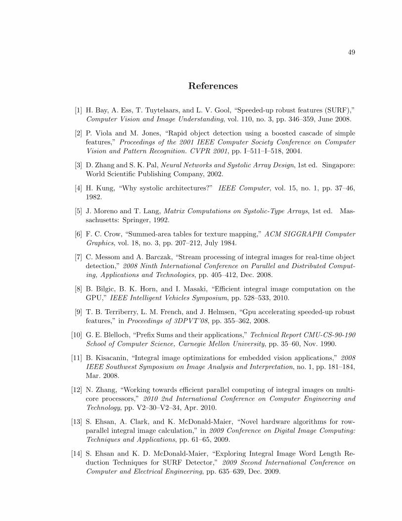
49
References
[1] H. Bay, A. Ess, T. Tuytelaars, and L. V. Gool, “Speeded-up robust features (SURF),”Computer Vision and Image Understanding, vol. 110, no. 3, pp. 346–359, June 2008.
[2] P. Viola and M. Jones, “Rapid object detection using a boosted cascade of simplefeatures,” Proceedings of the 2001 IEEE Computer Society Conference on ComputerVision and Pattern Recognition. CVPR 2001, pp. I–511–I–518, 2004.
[3] D. Zhang and S. K. Pal, Neural Networks and Systolic Array Design, 1st ed. Singapore:World Scientific Publishing Company, 2002.
[4] H. Kung, “Why systolic architectures?” IEEE Computer, vol. 15, no. 1, pp. 37–46,1982.
[5] J. Moreno and T. Lang, Matrix Computations on Systolic-Type Arrays, 1st ed. Mas-sachusetts: Springer, 1992.
[6] F. C. Crow, “Summed-area tables for texture mapping,” ACM SIGGRAPH ComputerGraphics, vol. 18, no. 3, pp. 207–212, July 1984.
[7] C. Messom and A. Barczak, “Stream processing of integral images for real-time objectdetection,” 2008 Ninth International Conference on Parallel and Distributed Comput-ing, Applications and Technologies, pp. 405–412, Dec. 2008.
[8] B. Bilgic, B. K. Horn, and I. Masaki, “Efficient integral image computation on theGPU,” IEEE Intelligent Vehicles Symposium, pp. 528–533, 2010.
[9] T. B. Terriberry, L. M. French, and J. Helmsen, “Gpu accelerating speeded-up robustfeatures,” in Proceedings of 3DPVT’08, pp. 355–362, 2008.
[10] G. E. Blelloch, “Prefix Sums and their applications,” Technical Report CMU-CS-90-190School of Computer Science, Carnegie Mellon University, pp. 35–60, Nov. 1990.
[11] B. Kisacanin, “Integral image optimizations for embedded vision applications,” 2008IEEE Southwest Symposium on Image Analysis and Interpretation, no. 1, pp. 181–184,Mar. 2008.
[12] N. Zhang, “Working towards efficient parallel computing of integral images on multi-core processors,” 2010 2nd International Conference on Computer Engineering andTechnology, pp. V2–30–V2–34, Apr. 2010.
[13] S. Ehsan, A. Clark, and K. McDonald-Maier, “Novel hardware algorithms for row-parallel integral image calculation,” in 2009 Conference on Digital Image Computing:Techniques and Applications, pp. 61–65, 2009.
[14] S. Ehsan and K. D. McDonald-Maier, “Exploring Integral Image Word Length Re-duction Techniques for SURF Detector,” 2009 Second International Conference onComputer and Electrical Engineering, pp. 635–639, Dec. 2009.

50
[15] H. Belt, “Word length reduction for the integral image,” in 15th IEEE InternationalConference on Image Processing, 2008., pp. 805–808, 2008.
[16] H. Belt and F. De Bruijn, “Storage size reduction for the integral image,” TechnicalNote TN-2007/00784, Phillips Research, p. 32, 2007.
[17] T. Gingold, “GHDL GNU VHDL simulator” [Online]. Available: http:
//ghdl.free.fr/.