Embed Size (px)
Citation preview
Field-enhancement of photoemission from cesium telluride
C. 1. Coleman
The responsive quantum efficiency of semitransparent cesium telluride photocathodes has been found to
be significantly increased by the application of high electric fields (a few MV m-1 ) such as are encounteredin proximity-focused image converters. Measurements of the magnitude of the effect are presented as func-
tions of applied field and of wavelength over the 120-800 nm range. An interesting anomaly was found in
the pair-production region in the vacuum uv; otherwise, the results are fairly consistent with the effects of
a simple Schottky lowering of the surface potential barrier of the photoemitter.
1. Introduction
The television camera detectors for the InternationalUltraviolet Explorer (IUE) satellite' use as input stagea proximity-focused uv-to-visible image converter(UVC). The UVC (ITT, type F4122) has a magnesiumfluoride entrance window on which is deposited a cesi-um telluride photocathode; useful response extends overthe 115-320-nm spectral range. The responsivequantum efficiency (QE), defined as the photoelectricyield in photoelectrons per incident photon, is of theorder of 0.15 over much of this range.
During the calibration of the IUE detectors, it wasnoticed that the shapes of the QE vs wavelength curvesinferred from the calibration data were different fromthose orginally obtained for the UVCs alone before theywere built into the cameras. Although the camerameasurements were subject to several inaccuracies, theyindicated a systematic trend toward an increase in theresponse at long wavelengths and a modification of theshape of the QE dip centered at -150 nm. As the UVCQE measurements are made using a low bias voltage (50V or 100 V, sufficient for saturation from the spacecharge point of view) while the cameras are operatedwith 5 kV between the photocathode and anode of theUVC, it seemed likely that field-enhancement effectsmight be responsible for the discrepancy. Some initialtests confirmed this hypothesis, and an extensive in-vestigation was then undertaken, the results of whichare reported below.
The author is with University College London, Department ofPhysics & Astronomy, London WC1E 6 BT, England.
Received 1 July 1977.0003-6935/78/0601-1789$0.50/0,© 1978 Optical Society of America.
Field-enhanced photoemission from metals (e.g.,potassium2) has been known for some time. More re-cently, these effects have been studied on the commonbialkali3 and trialkali4 6 photocathodes and also onsilicon and gallium arsenide negative-electron-affinitymaterials,7 The field enhancement in these casesreaches a maximum near the long-wavelength responsethreshold; typical peak enhancement factors over thelow-voltage QE for bialkali and trialkali photocathodesare about 5 at an applied field strength of 4 X 10⁶ Vm-1 .
11. The Cesium Telluride Photocathode
Cesium telluride is a solar-blind photoemissive ma-terial which has high QE in the uv combined with arelative insensitivity to visible light; its dark current(thermionic emission) is extremely low, and its long-term stability is excellent. The solar-blind character-istic is important in experiments such as IUE, wherestudies of faint uv spectra are to be carried out in thepresence of long-wavelength scattered light.
The responses of a large number of semitransparentCs2Te photocathodes in UVCs purchased for the IUEproject are remarkably similar to each other. A typicalmeasured QE curve (plotted on logarithmic axes) isshown in Fig. 1. The steep short-wavelength cutoff at-115 nm is due solely to the fall-off in transmission ofthe MgF2 window. At the long-wavelength limit of thehigh sensitivity region in the uv (the principal thresholdat around 330 nm), the response also decreases sharply,in this case because Cs2 Te is a semiconductor with acomparatively narrow bandgap.8 With increasingphoton energy (hv) above the principal threshold, theQE remains high (0.15-0.2, or sometimes greater, butnot as high as is achievable with an opaque Cs2 Te pho-tocathode) and is only slowly varying until a point isreached where hv is twice the bandgap energy and anadditional photoelectron energy loss mechanism,
1 June 1978 / Vol. 17, No. 11 / APPLIED OPTICS 1789
10
lo-l
QE
lo-4
Photon
10 8 6
100 120 150
energy (eV)
2
200 250 300
Wavelength Inm)
Fig. 1. Typical spectral response of a semitraluride photocathode on a magnesium flu
pair-production, becomes possible. yield then falls as the scattered elecbelow the photoemission threshold.crease in hp (i.e., towards even shorterincreasing number of scattered prima]electrons possess enough energy tophotocathode, and the QE starts to imechanism accounts for the pronouspectral response centered on -150 formation on Cs2Te and its band stru]from photoelectron energy distributicas a function of photon energy is given iof Taft and Apker9 and in more detail ipair-production energy loss effects are,photocathodes10"'. A consequenceportance in photoemissive imaging de,at high photon energies the emitteenergies are generally concentrated beand image resolution is not therefore sat short wavelengths. For Cs2Te, thi]ularly pronounced1 2 ; image resolution
with decreasing wavelength toward -150 nm and then,with the onset of pair-production, increases toward stillshorter wavelengths.
The Cs2Te response does not drop to zero in thevisible but exhibits a shoulder of finite sensitivity ex-tending to quite long wavelengths, as illustrated in Fig.1. The magnitude of this shoulder can be variable fromone sample to another and is reported to be correlatedwith the conditions of photocathode manufacture andresulting nonstoichiometry or the presence of more thanone phase of Cs2 Te.5 "3 QE measurements for thephotocathodes of the ITT F4122 tubes are typically 4X 10⁻⁴ at 400 nm, 6 X 10⁻⁵ at 550 nm, and fall fairlysteeply to 10-8 or less at the secondary threshold be-tween 700 nm and 850 nm. (Note that the term sec-ondary threshold, applied here to describe the long-wavelength cutoff, should not be confused with thethreshold for secondary electron production, whichoccurs at much higher photon energies.)
Uniformity of response is of importance in manyapplications. In these tubes, remotely processed andtransferred photocathodes are used, and the QE uni-formity is normally better than 5%. However, intubes where the photocathode processing was defectiveor where damage has been caused by contamination orby light overload, much larger wavelength-dependentnonuniformities become apparent; this point will bereturned to in Sec. V.
I I Illl. Experimental Procedure
400 500 600 70 0 The plane-parallel geometry of a proximity-focusedUVC provides an ideal experimental configuration forstudies of field-enhanced photoemission. The Cs2Tephotocathode, on an optically polished plane MgF2
nsparent cesiumtel- substrate, is spaced 1.3 mm from the anode. Theoride substrate. photocathode and anode surfaces are 40 mm in diame-
ter; thus, provided the illuminated area is less than -35mm in diameter, the electric field in the active volumeis perfectly uniform. At the usual operating voltage of5 kV, the field in the gap is 3.85 X 10⁶ V m-1 . The
'he photoelectric measured expansion of the gap for two UVCs whentron energies lie placed in an evacuated enclosure was 16.5 1 m (11/4%With further in- expansion); this necessitates a very small correctionwavelengths), an when comparing field enhancement measurementsries or secondary taken with the UVC in air (X > 194 nm) and in vacuoescape from the with a fixed applied voltage.rise again. This The experimental investigation was carried out.nced dip in the principally on two flight-standard UVCs (serial num-im. Further in- bers 11 75 04 and 12 75 05) and was divided into twocture as derived distinct parts: first, the determination of the absolutein measurements QE of the photocathodes at a low bias voltage over then the initial work 120-800-nm wavelength range and, second, relativen Ref. 8. Similar measurements of QE as a function of applied electricobserved in other field at a large number of points in the same wavelengthof practical im- range.vices is that evend photoelectron!low 2 eV or 3 eV,everely degradeds effect is partic-decreases slowly
A. Absolute QE Measurements
Ultraviolet QE measurements were made, at theScience Research Council's Culham Laboratory, bycomparison of UVC response with that of a standarddiode at 23 wavelengths between 120 nm and 337 nm.
1790 APPLIED OPTICS / Vol. 17, No. 11 / 1 June 1978
I I I I I I I I I
7
I I I I Il l
The light source was an air discharge, and a mono-chromator was used for wavelength selection. EachUVC was biased at 50 V (at the photocurrent levelsencountered, space-charge-saturated operation isachieved at 30-V bias or less); and a central 7-mm diamcircular area of the photocathode was illuminated. Thestandard diode was a Cs2Te cell originating fromStanford Electronics Laboratories (SEL)13 and cali-brated at the National Physical Laboratory (NPL)against two further SEL diodes, which had in turn beencalibrated at the U.S. National Bureau of Standards.The SEL diodes have been specially developed as uvradiation standards,13 and three out of four held by theIUE project in the U.K. are unchanged in relative sen-sitivity since their calibration in November 1974. Thereproducibility of the QE determinations for the UVCsin the uv is generally about 3%, but is nearer 10% at 130nm and 149 nm, where the Culham Laboratory's lightsource emits rather weak lines of somewhat variableintensity. The over-all accuracy of the absolute QEdetermination at short wavelengths, including theprobable error of the NPL calibration of the SEL diode,is thus about 7% over most of the wavelength range, butnearer to 12% in the region of the QE dip around 150nm. The wavelengths in this region at which QE canbe measured are 124 nm, 130 nm, 149 nm, 162 nm, and168 nm; thus, the detailed shape of the QE dip is notprecisely defined.
For wavelengths between 337 nm and 650 nm, in theshoulder region of the Cs2 Te response, QEs were mea-sured by comparison with an NPL-calibrated bialkaliphotodiode (EMI, type D127); this work was carried outat University College London (UCL). The UVC biasvoltage was 100 V, and the illuminated area was was acentral circle of 8-mm diam. A quartz-halogen lampwas used, and interference filters (AX = 6 nm FWHM;adequately suppressed outside the desired passband)were used for wavelength selection. Accuracy in thisregion was limited only by the calibration of the refer-ence photodiode, i.e., -2% at most wavelengths.
A few additional long-wavelength QE measurementswere made using the equipment designed by Wilcock1 4
at Imperial College. Here, the diameter of the illumi-nated area was 5.1 mm, and a 100-V bias was used. Thesystem is based on an NPL-calibrated standard tung-sten filament lamp and uses fairly broadband filters (AX-80 nm FWHM); this gives very accurate results pro-vided that the QE of the photocathode being measuredvaries only slowly over the filter bandpass. Because ofthe steeply falling QE characteristic of Cs2 Te at wave-lengths greater than 600 nm, the effective wavelengthat which the response is measured is shorter than thenominal wavelength of peak transmission of the filter;a first-order calculation gave corrected effective wave--lengths for the nominal 644-nm, 743-nm, and 795-nmfilters as 610-nm, 710-nm, and 755-nm, respectively.Because of this correction and because the photocur-rents were in any case so small, the accuracy of themeasurements was estimated as 30% at 710 nm and 50%at 755 nm. These measurements served as a check onthe earlier measurements at 455 nm, 525 nm, and 610
nm and enabled the range of the measurements to beextended beyond 650 nm, although with reduced ac-curacy.
It will be noted that QEs were measured over differ-ent areas of the photocathodes in the different wave-length regions. This, however, has negligible effect onthe results because of the uniformity of photocathoderesponse.
B. Field Enhancement Measurements
Field enhancement measurements in the uv (122-302nm) were carried out using the IUE vacuum opticalcalibration facility1 at UCL. The optical system con-sists of a light source feeding into a monochromator,which illuminates a small aperture; the aperture thenacts as a point source of monochromatic illuminationfor the UVC photocathode, which is situated about 1.5m away. Baffles in the optical system limited the illu-minated area of the UVC to a circle of 32-mm diam.There is a plane mirror in the optical path between theaperture and the UVC; by rotating the mirror (drivenby a stepper motor) through 900, the light may be-de-flected alternatively to a standard SEL photodiode.1 3
The mirror drive and the shutters in front of UVC andreference diode are normally computer controlled, butfor this experiment it was more convenient to operatethe mechanisms in a manual control mode. For shortwavelengths (up to 174 nm), the light source was a mi-crowave-excited hydrogen discharge; at longer wave-lengths, a high-pressure mercury discharge source withquartz envelope was used.
To measure small photocurrents with high biasvoltages on the UVC (up to 5 kV), a stable and noise-freeEHT supply was required; careful design of EHT wiringand connectors was necessary to minimize corona dis-charges. The EHT was continuously monitored usinga Fluke -100 high-voltage probe and digital voltmeter.The UVC photocurrent (typically 10-11 A) was mea-sured by a Keithley picoammeter (type 410A) whoseoutput was fed to a chart recorder; the latter made iteasy to average over the residual system noise so steadyphotocurrents could be determined to an accuracy of-10-13 A.
The procedure for taking a series of measurementsat any one wavelength was as follows. After setting thebias voltage and allowing the necessary settling time(about 3 min after a large voltage change), a reading wastaken from the reference photodiode. Simultaneously,the UVC dark current was recorded. The light wasthen switched from the photodiode to the UVC, and thephotocurrent (including dark current) was recorded forabout 1 min. The light was then switched back to thephotodiode, and another reading was taken togetherwith a second recording of the UVC dark current. Theinitial bias voltage setting at each wavelength was 100V; the sequence was repeated at 200 V, 500 V, 1 kV, 2kV, 3 kV, 4 kV, and 5 kV, giving a total of eight sets ofreadings at each wavelength. At each voltage, themeasured photocurrent was corrected by subtractingthe dark current and then normalized to a standardreference photodiode reading to account for any fluc-
1 June 1978 / Vol. 17, No. 11 / APPLIED OPTICS 1791
6 4 3.5 3
Photon energy (eV)
2.5 2.2 2 1.8 1.6 1 55 10-3
200 300 400 500 600 700 800
Wavelength (nm)
200 300 400 500 600 700 800
lo-6
10-,
lo-8
Wavelength (nm)
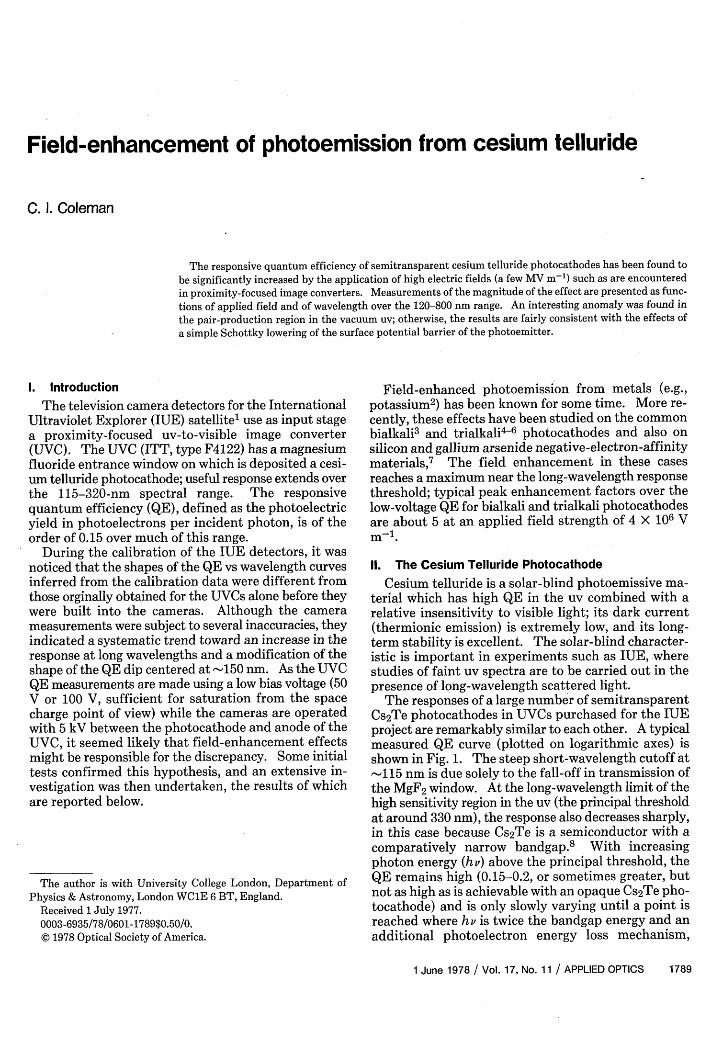
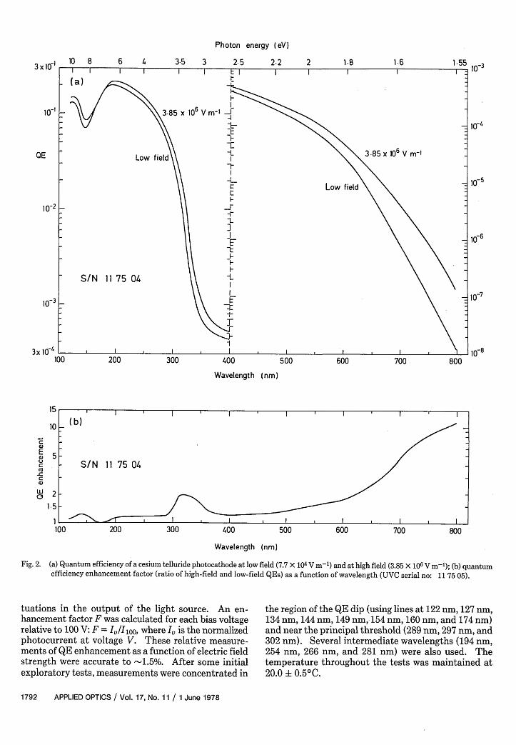
Fig. 2. (a) Quantum efficiency of a cesium telluride photocathode at low field (7.7 X 10⁴ V m-1 ) and at high field (3.85 X 10⁶ V m-'); (b) quantumefficiency enhancement factor (ratio of high-field and low-field QEs) as a function of wavelength (UVC serial no: 11 75 05).
tuations in the output of the light source. An en-hancement factor F was calculated for each bias voltagerelative to 100 V: F = v/I100, where I is the normalizedphotocurrent at voltage V. These relative measure-ments of QE enhancement as a function of electric fieldstrength were accurate to -1.5%. After some initialexploratory tests, measurements were concentrated in
the region of the QE dip (using lines at 122 nm, 127 nm,134 nm, 144 nm, 149 nm, 154 nm, 160 nm, and 174 nm)and near the principal threshold (289 nm, 297 nm, and302 nm). Several intermediate wavelengths (194 nm,254 nm, 266 nm, and 281 nm) were also used. Thetemperature throughout the tests was maintained at20.0 I 0.50 C.
1792 APPLIED OPTICS / Vol. 17, No. 11 / 1 June 1978
3 x 1-l-,
QE
10-2
lo-3
3 x lo-4
10 8
100
15
10
54EUC(U_-_C63
w03 2-
1 0100
Photon energy
4 3.5 3 25
200 300 400
2.2 2 18
500 600
Wavelength (nm)
15
z
c
63
EUC
C63
wC
Wavelength (nm)
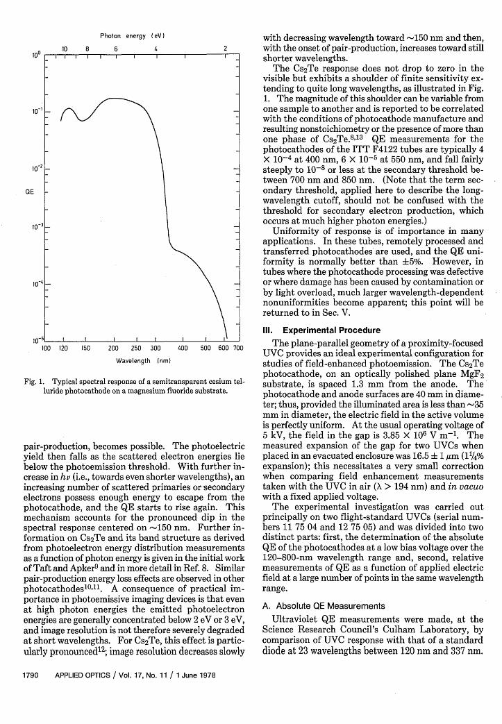
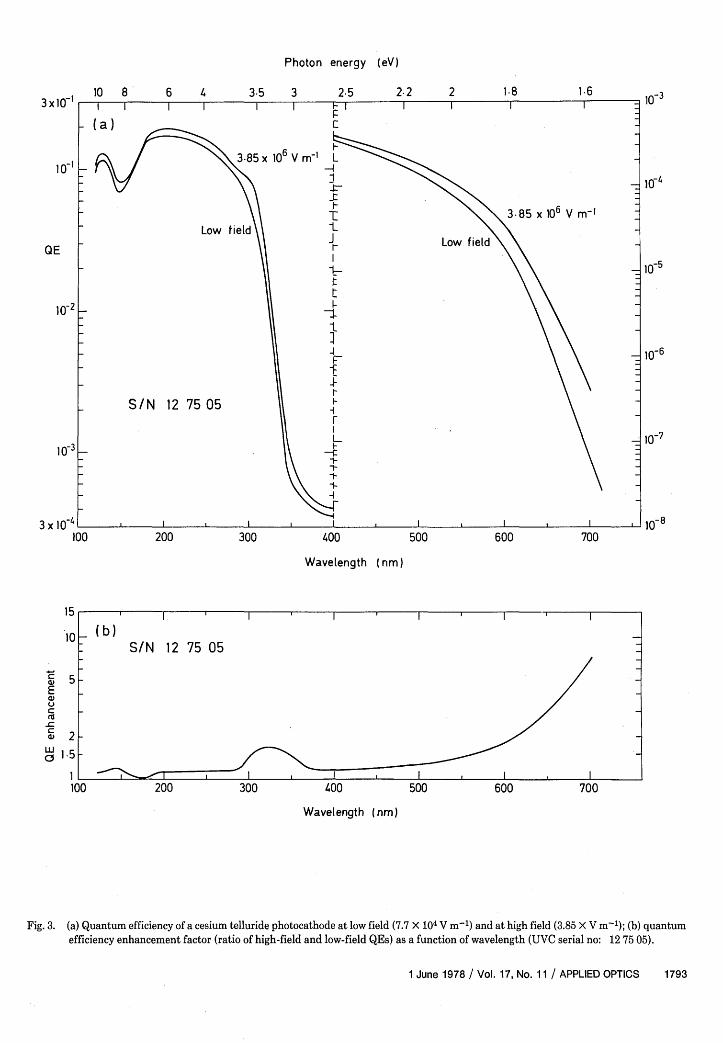
Fig. 3. (a) Quantum efficiency of a cesium telluride photocathode at low field (7.7 X 10⁴ V m-1) and at high field (3.85 X V m-1 ); (b) quantumefficiency enhancement factor (ratio of high-field and low-field QEs) as a function of wavelength (UVC serial no: 12 75 05).
1 June 1978 / Vol. 17, No. 11 / APPLIED OPTICS 1793
10 8 63 x 10-
10-1
QE
10-2
10-3
3 x 10⁻⁴
Xa g > \ :b~3. x 6 V m-1 L
Low field\t\\\ ~~~~~~~~Low f ield
S/N 12 75 05 F\
-\ V \\ L
l l l l l l l l l l l~~~~~~~~~~~~~~~~~~~~~-
1 .6
700
10-3
1o0L
lo-7
10-8100
_ , , , , , , - T
(eV)
Measurements at longer wavelengths were carried outusing a similar experimental setup, but with a simpleroptical system. Narrowband interference filters wereused instead of a monochromator, and there was noreference photodiode. To obtain accurate results, it wastherefore necessary to repeat several readings in eachseries to check that the light source output remainedconstant. It is estimated that the residual error in Ffrom light source instability was 4% using a mercurysource and 2% using a quartz-halogen lamp. Consis-tency between the results obtained with this setup(where the illuminated area of the UVC was 20 mm indiameter) and those obtained with the vacuum opticalsystem was confirmed by repeating the work at 194 nmand 254 nm. The measurements in the region of theprincipal threshold were completed using furthermercury arc lines at 313 nm and 334 nm. Measure-ments in the shoulder region were carried out at thefollowing wavelengths: 385,408,418,457,499,546,589,602, 655, 698, and 798 nm; these were mostly with thequartz-halogen source, and the FWHM bandwidth wastypically 6 nm.
IV. Results and Discussion
A. Absolute Quantum Efficiency
The absolute low-field QEs for the two UVCs whichwere the principal subjects of this investigation areshown in Figs. 2(a) and 3(a). Note that because of theseven-decade range of QE values, the graphs are dividedinto two portions with different scales for wavelengthson either side of 400 nm. The two UVCs have fairlysimilar QE curves, although that for S/N 12 75 05 hasa slightly steeper principal threshold, and a shoulderwhich is only marginally lower up to 600 nm, but is lowerby a factor of 10 at 700 nm. The quantum yields forthese two photocathodes are typical of those for the UEflight-standard tubes.
As was pointed out in Sec. III. A, the shape of the QEdip is not well defined by the Culham Laboratorymeasurements. Some additional uv QE data were ob-tained by using the reference photodiode readings fromthe measurements in the UCL vacuum optical calibra-tion facility. The results for the several wavelengthsavailable with the UCL system in the region of the dip
1 2 3 4
1 2 3 4
1.3
1.2 1
1.1
1.01
1.6
1.4
1 .2
1 .0
i :
J 1 2 3 4
,* 0
1.4
1.2.
1.0
1 2 3
I.
1 .;
1.1
1 *(4
1. 3
1.2
1.1
0
n
) 1 2 3 4
1 2 3
I I '
385 nm
, ,
0 1 2 3 i
7
5
3
0 1 2 3 4 0 1 2 3
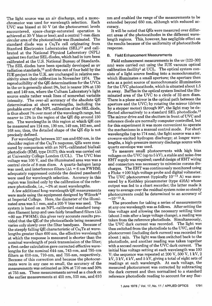
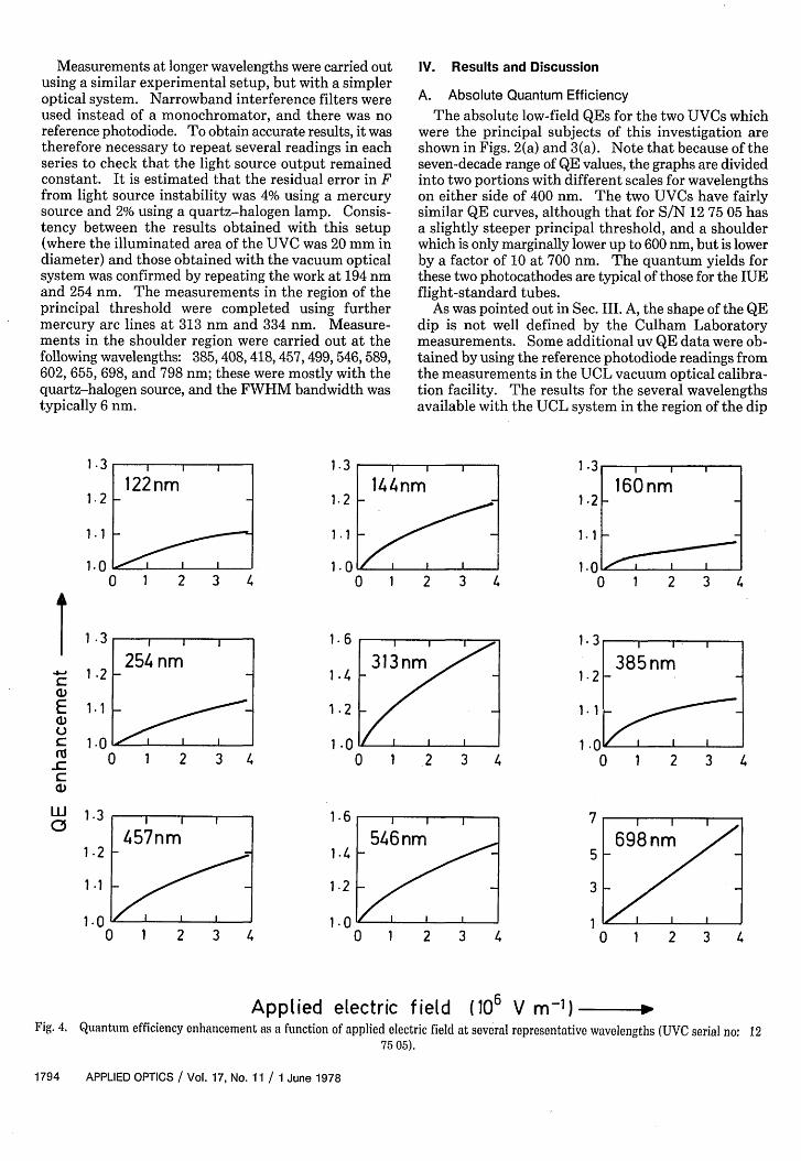
Applied electric field (106 V m ) -Fig. 4. Quantum efficiency enhancement as a function of applied electric field at several representative wavelengths (UVC serial no: 12
75 05).
1794 APPLIED OPTICS / Vol. 17, No. 11 / 1 June 1978
1.1 I
122nm
1 2 I
1.3
1 21
C
1 .3
1 n m144nm
I, I
I I I
254 nmA, ,~~~~~~~~~~~~~~~~~~~~~~21t60 nm
l6Onrn
313 nm
/, I
.4-,C:a)Ea)UC-c-Ca)
LUa3
4
.21
1.1
.0 C
1.3
1.2
1 .1
1.0
457nm
- I
546nm
_
698 nm I_ I
4
I
1 *:
To To
1
1I
1I 4
I
suggest that, for UVC 12 75 05 only, the minimum of thecurve should be shifted by about +3 nm with respect tothat shown in Fig. 3(a) and that the QE at the minimumwas over-estimated by about 10%. Any uncertainty inthe absolute QE does not, of course, affect the validityof the relative enhancement measurements reportedbelow. At all other wavelengths up to 300 nm, there wasexcellent agreement between the Culham QEs for bothphotocathodes and those inferred from the UCL stan-dard photodiode readings.
B. Field Enhancement of Quantum Efficiency
The magnitude of the enhancement factor F and theform of its dependence on applied electric field E aredifferent at different wavelengths. F vs E plots atseveral representative wavelengths are shown in Fig. 4for UVC S/N 12 75 05. Broadly similar results wereobtained for UVC S/N 11 75 04. There is no enhance-ment whatsoever at 174 nm for either UVC. At allother wavelengths (Fig. 4, and other plots too numerousto be reproduced here), the dependence of enhancementon applied field at wavelength X can be reasonably welldescribed by functions of the form: F = 1 + axE/ 2 +bxE, as suggested by Guth and Mullin'5 for metallicphotoemitters. Note that at the secondary threshold(698 nm for S/N 12 75 05; 798 nm for S/N 11 75 04), theenhancement is greater than at any other wavelengthand F is linearly related to E (bottom right graph in Fig.4). Periodic deviations'5 from the straight line de-pendence at the secondary threshold do not exist at the2-3% level (the scatter of the experimental points); itmight be interesting to repeat this part of the experi-ment with higher precision (with a monitor for the lightsource output).
The QE enhancement factor at the highest field used(3.85 X 10⁶ V m-1) is plotted as a function of wavelengthfor both photocathodes in Figs. 2(b) and 3(b); the curvesare qualitatively very similar. In Figs. 2(a) and 3(a), thehigh-field QE curves (the product of the low-field ab-solute QE and the enhancement factor) have beenplotted as well as those for low field. The increasedenhancement factor in the region of both the principaland secondary thresholds is readily understandable interms of a simple shift of threshold caused by a Schottkylowering of the surface potential barrier by the appliedelectric field, thereby increasing the escape probabilityof photoelectrons generated in the Cs2Te layer. Thereduction AO (in volts) of the potential barrier is easilyshown to be AO = (qE/47re0)"/2 , where q is the electroniccharge and E0 is the permittivity of free space. For E= 3.85 X 10⁶ V m-1 , the value of AO is 0.074 V. By in-spection of Figs. 2(a) and 3(a), using the upper photonenergy scale, it may be seen that the magnitude of theshift at both thresholds and indeed over most of theshoulder region is in reasonable agreement with thesimple calculation.
While the field enhancement is fairly constant (F1.16) over much of the range of useful sensitivity in theuv, an anomaly is apparent in the region of the QE dip.At the point where the QE starts to rise on the short-
wavelength side of the dip (145 nm), the enhancementpeaks at a value of F 1.22; this is qualitatively expli-cable again in terms of the reduction of the surface po-tential barrier with consequent increase in the escapeprobability of both scattered primaries and secondaryphotoelectrons. On the long-wavelength side of the QEdip (-174 nm), no enhancement whatsoever is observed(F = 1.005 ±0.01 for both photocathodes).
The following explanation of this anomalous behaviorhas been proposed by Spicer and Powell.'6 In additionto decreasing the potential barrier height, the high field(which can penetrate into the semiconductor) deflectsthe trajectories of primary electrons toward the surface.Thus, a percentage of primary electrons which wouldnot have been in the escape cone before the high fieldwas applied is now able to escape; this effect may beresponsible for most of the 16% field enhancement ofQE observed in the near uv. The increased trajectoryalso results in a greater probability of scattering withvalence-band electrons; this is of no consequence below6.8 eV, but above 6.8 eV the onset of inelastic scatteringcould remove more primaries from the yield than areadded due to the deflecting effect of the high field. Thiswould account for the net decrease in F at around 174nm.
It is worth mentioning that, even in the absence ofexternal field, photoelectrons with insufficient mo-mentum normal to the surface can be scattered into theescape cone by successive phonon collisions. In thinsemitransparent photocathodes, photoelectrons canreach the interface with the substrate and be lost beforea sufficient number of phonon collisions have been ex-perienced. Hence, the yield of semitransparent Cs2Te(typically <20% in the near uv-Fig. 1) is considerablyless than found for opaque Cs2Te (50% in the samespectral range'3 ) because of the greater opportunity forphonon scattering in the latter case. One mighttherefore expect the anomalous behavior in Cs2Te near7 eV to be less pronounced in opaque films since, in thiscase, a large fraction of primaries have already beenscattered into the escape cone by phonon collisionsalone.
C. Dark Emission of Cs2Te
The dark currents measured during the experimentsdescribed above are predominantly leakage currents inthe UVC and its encapsulation; they vary approximatelylinearly with applied voltage, amounting to about 10-"1A at 5 kV. The true dark emission of the Cs2Te pho-tocathode is very much smaller than this value. Thereis a dearth of information on this subject in the litera-ture. The data of Williams and Feibelman' 7 yield anupper limit of 25 electrons cm-' sec' in a Bendixproximity-focused converter at room temperature andwith an applied field of 3.0 X 10⁶ V m-1 . Stephan andSamuelsson1 8 give a figure of 80 electrons cm- 2 sec1for the dark current of a Cs2Te photocathode in a de-velopmental English Electric triode image converter.From published information on this latter tube,' 9 it is
1 June 1978 / Vol. 17, No. 11 / APPLIED OPTICS 1795
estimated that the field strength at the photocathodewas only 1-2 X 10⁵ V m-1 , and it is surprising that thedark emission should have been so very high.
The dark emission of the ITT F4122 tubes is assessedroutinely at UCL by measuring the photon flux from theUVC's phosphor screen with a calibrated photomulti-plier in the absence of any light input to the UVC pho-tocathode. As the phosphor screen gain (photons perelectron) as a function of applied voltage is also mea-sured for each UVC, it is a simple matter to calculate theelectron flux from the photocathode. The dark emis-sion measurements are carried out at 200C and with anapplied voltage of 5.9 kV (field strength 4.54 X 10⁶ Vm-1), and typical emission currents are between 1-3electrons cm-1 sec-1. An analysis of data for elevenUVCs has shown that there is no correlation betweenthe measured thermionic emission of these photocath-odes and their QEs at either the principal or the sec-ondary threshold. Measurements have been made fortwo UVCs at 5 kV as well as at 5.9 kV, and the emissionis less by a factor of -1.3 at the lower voltage. This isconsistent with the emission being a field-enhancedthermionic current. If the work function 0 in theRichardson equation for thermionic emission I = AT2
exp(-O/kT) is modified to 0 - AO5 [where AO = (qE/47re,, )1/2 is the reduction in surface potential barrier byan applied electric field E, as in Sec. IV.B above], it iseasily shown that the field-enhanced thermionic emis-sion I(E) is proportional to exp(0.44E'/ 2/T). Onewould therefore expect the low-field thermionic emis-sion to be less than the 5.9-kV value by a factor of about25. These very low thermionic emission figures forCs2 Te at room temperature (about a factor of 100 lowerthan for a bialkali photocathode) are as would be ex-pected for a photoemitter which is insensitive to longwavelength light.
V. Conclusion
There is good agreement between the results obtainedwith the two UVCs; spot tests on other UVCs togetherwith the trends indicated by the IUE camera calibrationdata all suggest that the results are fully representativefor semitransparent Cs2Te photocathodes of the samemanufacture. There is no reason to believe that theresults should not be applicable at least qualitativelyto other Cs2Te photocathodes except that, in the caseof opaque photocathodes, the contribution to F due toelectron deflection (and hence the anomalous behavioraround 174 nm) would be expected to be less pro-nouned, as discussed in Sec. IV.B.
It is interesting to note that there is a striking corre-lation between the field enhancement curves [Figs. 2(b)and 3(b)] and the wavelength dependence of photo-cathode nonuniformity. The latter has been measured,above 254 nm, on two Cs 2Te photocathodes. In one ofthese, there was evidence of partial shadowing duringmanufacture; and, in the other, the nonuniformity wasdue to excessive illumination of one-half of the photo-cathode area. In both cases, the nonuniformity peakedat a value of 40% in the region of the principalthreshold, fell to less than 10% around 400 nm, and then
gradually rose to greater than 50% near the secondarythreshold. According to Fisher et al.,'1 it is commonalso to see a peak in the nonuniformity at 8.5 eV; thiscorresponds to the wavelength (145 nm) at which fieldenhancement reaches a maximum in the QE dip region.The dependence of photoelectric yield on potentialbarrier height explains why both nonuniformity (arisingfrom spatial variations in barrier height due to slightchanges in photocathode structure or composition) andfield enhancement (variation of barrier height throughapplication of electric field) should behave so similar-ly.
In summary, it has been shown that the QE of a Cs2Tephotocathode, as used in the IUE cameras, is usefullyenhanced by about 16% over most of its working rangein the uv. The thermionic dark current remains neg-ligible at high field, but the solar blindness is reducedby large factors at long wavelengths.
Many colleagues in the IUE project team renderedinvaluable assistance at various stages of this work; theauthor particularly thanks B. Anderson, M. Courthold,D. John, M. Trower, R. Webster, and U. Yilmaz.Thanks are also due to R. Airey of the Blackett Labo-ratory, Imperial College of Science and Technology, forhis help in providing additional long-wavelength QEmeasurements.
References1. K. G. R. Allen, B. E. Anderson, A. Boksenberg, and M. B. Oliver,
Adv. Electron. Electron Phys. 40A, 223 (1976).2. E. 0. Lawrence and L. B. Linford, Phys. Rev. 36, 482 (1930).3. J. A. Cochrane, English Electric Valve Company; private comg-
munication (1977).4. K. R. Crowe and J. L. Gumnick, Appl. Phys. Letter. 11, 249
(1967).5. R. S. Florek and L. 0. Owen, Bendix report OSD 1366 (1970).6. J. A. Cochrane and R. F. Thumwood, Adv. Electron. Electron
Phys. 40A, 441 (1976).7. J. R. Howorth, A. L. Harmer, E. W. L. Trawny, R. Holtom, and
C. J. R. Sheppard, Appl. Phys. Lett. 23, 123 (1973).8. R. A. Powell, W. E. Spicer, G. B. Fisher, and P. Gregory, Phys.
Rev. B. 8, 3987 (1973).9. E. Taft and L. Apker, J. Opt. Soc. Am. 43, 81 (1953).
10. L. Apker, E. Taft, and J. Dickey, J. Opt. Soc. Am. 43, 78(1953).
11. W. E. Spicer, J. Phys. Chem. Solids 22,365 (1961) and referencescited therein.
12. A. Boksenberg, in Astronomical Observations with Television-Type Sensors (Institute of Astronomy and Space Science, U.British Columbia, Vancouver, 1973) p. 311.
13. G. B. Fisher, W. E. Spicer, P. C. McKernan, V. F. Pereskok, andS. J. Wanner, Appl. Opt. 12, 799 (1973).
14. W. L. Wilcock, Adv. Electron. Electron Phys. 22A, 535 (1966).15. E. Guth and C. J. Mullin, Phys. Rev. 59, 867 (1941).16. W. E. Spicer and R. A. Powell, Stanford Electronics Laboratories;
private communication (1977).17. J. T. Williams and W. A. Feibelman, Appl. Opt. 12, 2832
(1973).18. K. H. Stephan and H. Samuelsson, Appl. Opt. 14, 2668 (1975).19. B. R. Garfield, European Space Research Organisation Contractor
Report ESRO CR-217 (1974).
1796 APPLIED OPTICS / Vol. 17, No. 11 / 1 June 1978