Embed Size (px)
Citation preview

VLA Electronics Memo # 244
Fiber Optic Transmitter/Receiver Duplication for the Pie Town Link
Kurt Caviggia August 15, 2002

Caviggia9/10/2002
Page 2 o f 33
Abstract: In this National Radio Astronomy Observatory Co-op project, completed during the summer of 2002, two spare modules were constructed for the Very Large Array Pie Town link. The Pie Town Optic link combines astronomy data from the Very Long Baseline Array with the VLA to give increased resolution. An optical transmitter and receiver pair were constructed to provide support to the existing modules. The transmission system uses a 50 mW laser and an external modulator to transmit four IF signals a distance of 104 km. In this report module design is covered along with artwoik, drawings, and schematics used in the construction. Troubleshooting setups and methods are discussed. Finally, a detailed list of parts and prices are included along with datasheets.

Caviggia9/10/2002
Page 3 of 33
Table o f Contents
1. Introduction.................................................................................. ... 51.1 Pie Town to VLA Fiber Optic Link..............................................51.2 Pie Town Link: Transmit and Receiver Modules........................6
2. Co-op Project................................................................................ ...82.1 Project Description...................................................................... ..82.2 Tasks and Goals.......................................................................... ...9
3. Module Design.............................................................................. ... 103.1 Analog Fiber Transmitter.............................................................. 103.2 Analog Receiver Unit................................................................. ...12
4. Module Construction..................................................................... ..144.1 Building the T203........................................................................ ..144.2 Building the T202........................................................................ ..17
5. Testing............................................................................................. .205.1 Bench Tests.....................................................................................205.2 Field Tests.......................................................................................23
6. Conclusions..................................................................................... .256.1 Final Results...................................................................................256.2 Comments..................................................................................... ..26
Appendix A: List of Parts and Prices............................................. ..27Appendix B: Schematics and Diagrams....................................... ...27Appendix C: Data Sheets............................................................... ....35

Caviggia9/10/2002
Page 4 o f 33
List o f Figures
Figure 1: Pie Town to VLA Block Diagram...................................................... 6Figure 2: Transmit and Receive Overview........................................................ 7Figure 3: Current Transmit/Receive pair at the site........................................... 8Figure 4: Determining the Dynamic Range....................................................... 11Figure 5: SBS Launch Power............................................................................ 12Figure 6: Typical Received VLA Signal............................................................ 13Figure 7:T203 Pins and Connections................................................................ 15Figure 8:Typical Losses for Coax..................................................................... 17Figure 9: T202 Pins and Connections................................................................ 19Figure 10: Test Setup Diagram.......................................................................... 21Figure 11: Laser Wavelength and Power............................................................ 22Figure 12: Received Signal Comparison............................................................ 24Figure 13 Constructed Spares............................................................................. 26

Caviggia9/10/2002
Page 5 o f 33
1. Introduction
This section describes the function of the entire Pie Town (PT) to Very Large Array
(VLA) link as well as how the transmitting and receiving is accomplished.
1.1 Pie Town to VLA Fiber Optic Link
The purpose of the Pie Town optic link was to combines the astronomy data of
Very Long Baseline Array (VLBA) with data from the VLA. The present
resolution in the VLA was increased to provide astronomers with a sharper
image. It should be noted that Pie Town link is only functional when the VLA is
in an “A” configuration. In other words, the VLA antennas are positioned to the
max distance on each arm (27 km). This link adds 27 Baselines to the array,
keeping the origin at the center of the VLA.
There are four IF signals generated in VLBA format (between 500 MHz - 1000
MHz) at the Pie Town Antenna. These signals are converted, at Pie Town, to a
50 MHz wide VLA signal. The four signals are multiplexed and then modulated
onto a single laser. The signal is transmitted over 104 km of fiber to the VLA
site. Once the signal arrives at the site, it is received and converted back into an
RF signal. The final RF signal is sent to the existing backend of the VLA.
A block diagram illustrating the PT to VLA link can be seen below in Figure 1.

S'rS
TfM
Caviggia9/10/2002
Page 6 o f 33
X:: fi.PIE TOWN to VLA Link
B ase lin e 5 2 km
BaikK v idMt 9X1MB* S'?;
(A/5
* s>
<8>
AJ2-5MJH£
J
m tea 1 \1425MMC
U G L J o £ l J > <8>
00*1 Oscdfatfwvtt
f t i.RxK 1.0CIWN
| Anaki*| Fiber Trau^miucr I Precision \I M Z m odulated 1 I>FB
12 0 0 M H z P TM a se r D e riv e d
i O P T IC A LX
| M U X
Datecoinm*FJhrrodI'thcmet
Fife*rPilitiiT h u itc n iv e r
M U X
D irectlyModulatedD F t t
SQGM b/sec
P I E T O W N
1 Q4Scm Standard Singiemosite Fiber D ~ \ 8?Op«/nm
Tr*M«*-«iv«r mdMUX
D irectly \*--------------------------Modwrtated \ ~
D F B j------ ‘Spare I/O800M h/*ec j
- VLA cjrete sync
L'UKomm*BlKIUttf.Sthcrwe*
V L AR o n B e re s to rd Sep9 9
Figure 1: Pie Town To VLA Block Diagram
1.2 Pie Town Link: Transmit and Receiver Modules
An essential part of the Pie Town Link is the Fiber Optic Transmitter and
Receiver Modules. The purpose of these modules is to take an Analog
multiplexed signal (Converted from VLBA format to VLA format) and
externally modulate the signal on to a laser (using DWDM). The laser operates
at a wavelength of 1555 nm, which can be tuned using a thermal controller. The
signal is then sent over 104 km of fiber, using fiber from Western New Mexico
Telephone Company (WNMT), to the VLA site.
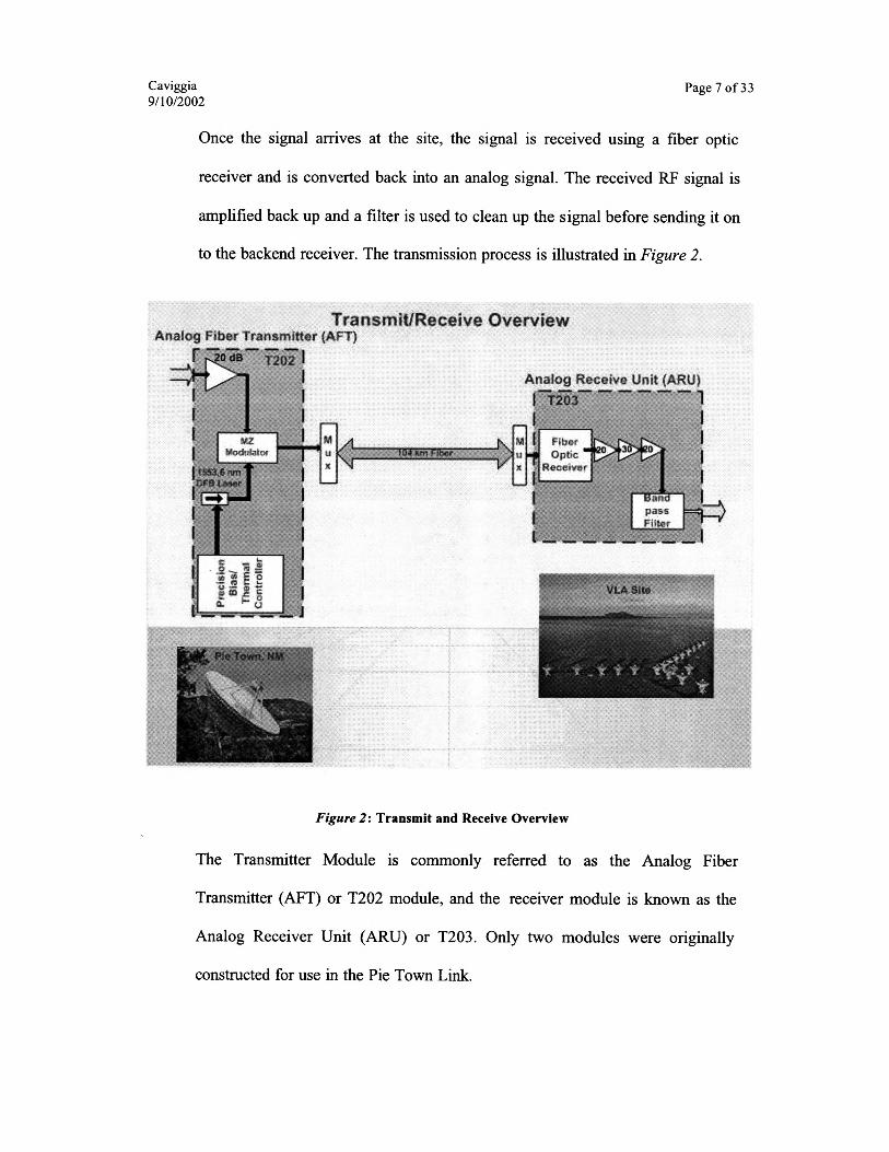
Once the signal arrives at the site, the signal is received using a fiber optic
receiver and is converted back into an analog signal. The received RF signal is
amplified back up and a filter is used to clean up the signal before sending it on
to the backend receiver. The transmission process is illustrated in Figure 2.
Caviggia Page 7 of 339/10/2002
Transmit/Receive Overview{AFT}
:
Figure 2: Transmit and Receive Overview
The Transmitter Module is commonly referred to as the Analog Fiber
Transmitter (AFT) or T202 module, and the receiver module is known as the
Analog Receiver Unit (ARU) or T203. Only two modules were originally
constructed for use in the Pie Town Link.

2. Co-Op Project
This section describes the project assigned and some of the required tasks and project
goals.
2.1. Project Description
The Pie Town link only has a single T202 and T203 module. Since there are no
spares for these modules, in the event of a failure in either module, the entire PT
link is shut down. Due to demand for less downtime, a spare for both modules
was required. Along with creating duplicate modules, documentation for each
part along with detailed schematics and pricing was required. Figure 3 shows a
picture of the insides of the T202 and T203.
Caviggia Page 8 of 3 39/10/2002
Figure 3: Current Transmit/Receive pair at the site.

2.2. Tasks and Goals
In order to get the most out of the project, the following set of tasks was defined:
improvements, time restraints, and budgeting issues. Also, there are certain goals that
must be completed. Therefore, a set of objectives was made and divided up in to
required tasks and project goals:
I. Required Tasks
> Use in-house parts to reduce costs.
> Spare must fit in a singlewide module slot.
> Provide documentation and testing procedures.
> Spares must be identical to the original modules.
> Order more replacement parts.
> Build both modules before the end of July 2002.
II. Project Goals
> Improve upon the existing design.
> Reduce future problems by extensive testing.
> Continual use of both spares after construction.
Caviggia Page 9 of 339/10/2002

3. Module Design
This section describes how the original modules were designed. The choice of
components and a characterizing of the current Pie Town Link Signals are included in
this section. The engineer in charge of this design was Ron Beresford.*
3.1. Analog Fiber Transmitter
The Optical Transmitter is designed to transmit four externally generated IF
signals over 104km of fiber. The method of external modulation with a high
power CW laser was chosen over direct modulation. “By externally modulating
an ultra-stable CW laser with an MZ modulator wavelength chirping is
eliminated. Increasing CW laser power will reduce the link noise figure” 1. A
problem with using external modulation is there is a high insertion loss (around
5 dB or greater). Initial tests were done with a 90 mW laser to provide sufficient
drive. Testing determined that a minimum power output from the transmitter is
8.8 dBm.
Choosing a dynamic range is an important factor in the design of the
transmitter. The signal to noise ratio (SNR) is around 20 dB, since this is
“adequate for digitization and good astronomy” 1. Also, headroom of 10 dB was
chosen to make “Dynamic Range as large as reasonable achievable” f. This
gives a required dynamic range of 30 dB (20 dB SNR + 10 dB headroom). A
graph showing the design of dynamic range is found in Figure 4.
* Information quoted in this essay conies from Ron Beresford’s report “RF Fiber Optic Link” found in the Pie Town Hand Book.
Caviggia Page 10 of 3 39/10/2002

Caviggia9/10/2002
Page 11 of 33
Modulation Ft* quency MHz
Figure 4: Determining the Dynamic Range
Another important design issue was the effects of the Stimulated Brillouin
Scatter (SBS). This effect, which is non-linear, happens in narrow line width,
high power systems over long distances. The forward wave interacts with
vibrating molecules in the glass causing a backward traveling wave, which
causes power losses and decreases the SNR. Figure 5 on the following page
shows the required launch power as a function of distance. Based on this plot, a
launch power of 8 dB was needed to ignore the effects of SBS. A 50 mW DFB
laser was bought with a Hybrid Temperature Controller (HTC) to stabilize and
adjust the frequency. Also, a PLD-500 was bought to control laser bias.

Caviggia9/10/2002
Page 12 of 33
u,$oPh
oah-i£Vis4>Ph
,.50.882 M 60
52.5
45
? cw1;1 37.5
30
22.5
15
7.5
0
J
SBS Profile
vi,2
-4.819,
••
••
••
•»
•
....
V ** . • « • • ♦ • • ♦ -------- • •
...........
. . . . . . . .
10 20 30 40 50 60 70 80 90 100 110 120 F i b e r L e n g h t •
Figure 5: SBS Launch Power
3.2. Analog Receiver Unit
Two important design considerations are low noise and receiver sensitivity. In
order to keep the SNR down, the first amplifier must always be a low noise
amplifier. “CAD modeling revealed that there is a one for one relationship
between the noise figure of the amplifier immediately proceeding the PIN
detector and the noise floor of the link”*. The first stage amplifier was chosen to
be a low noise amplifier from Mini-Circuits. The max power received in the
link is determined by the sensitivity of the photodiode. The receiver that is
currently used in Pie Town has a sensitivity of 0.8 mA/mW.
A problem in the original design was impedance matching. The output
im p e d a n c e o f th e p h o to -d e te c to r w a s 5 0 0 £2, w h ic h w a s m a tc h e d w ith a 5 0 £2

Caviggia Page 13 of 3 39/10/2002
input on the amplifier. This impedance mismatch might cause reflections and
losses. A solution would be to build a low-loss broadband transformer, but
“Vector analysis of the mismatched configuration revealed excellent 50 MHz
pass bands for A, B, C, and D channels. Resistive matching was not required”*.
A good received signal at the VLA site contains the proper phase delay and
amplitude. All four bands including the 1200 MHz syncing tone should be
received at levels around -25 dBm. The signal was found by characterizing the
receiver at the VLA site. Also, some tweaking of the L6 oscillators at Pie Town
was required. A spectrum capture a good of a Pie Town Transmitter/Receiver
signal is shown in Figure 6.
Figure 6: Typical Received VLA Signal

4. Module Construction
This section describes the construction of a two modules based on the current design in
use at Pie Town. Details on the construction and design choices involved are included.
4.1. Building the T203
A trip to the VLA and Pie Town was required to get information on how both
modules were built, and to acquire parts for building spares. Both modules were
designed for a singlewide VLA slot, with OSP RF connectors on the back for
simple connection. The hardware for building singlewide modules such as the
chassis and the railing was found at the VLA. Finally, a front panel for both
modules had to be drawn and sent to the machine shop.
The first module to be built was the T203. The chassis was assembled using
parts from the site and the Array Operations Center (AOC). A pin-out of the
back panel of the T203 chassis showing both connectors and wires can be found
in Figure 7. Once a chassis was built, a layout of components was devolved.
Appendix B, Figure 1 shows component arrangement. A 20 dB, low-noise, and
a 30 dB amplifier (all manufactured by Mini-Circuits) were taken to build this
module. Since these were the last amplifiers, an order for extras was placed.
Also, a different receiver was used in this project. A Small Integrated Receiver
Unit (SIRU) SIRU 2300 from JDS Uniphase was used instead of the SIRU
1114. The receiver has a sensitivity of .85 A/W compared to .8 A/W in the
original module. A problem presented by using the SIRU 2300 was it was a bit
bigger than the unit used in the original.
Caviggia Page 14 of 3 39/10/2002

Caviggia9/10/2002
Page 15 of 33
__Fiber Input- SC ConnectorDiamond, Inc.IIYB-S1L2 i.SH.’F C -lf {Kr> 0 -2 ram) Order Nmnbrn 1*5-311-W7V022
OSP RF Output NVA-COM PM 4503-7941-00
\ Black: GroundLocation B
\ Red: »15 Volts Power Location A
Power Input Shield Amp P/N 201350-2 Block Amp P/N 200838-3
Figure 7: T203 Pins and Connections
A front panel had to be constructed to hold a Digital Panel Meter (DPM) a
power LED, and a SMA test point. Both modules had the same setup; therefore
the front panel design was used for both modules. The lead-time on the front
panel construction was between two and three weeks. Appendix B, Figure 2
shows the final drawing used for the front panel.
The choice to use a terminal strip to power the amplifiers and the receiver was
made. A terminal strip can be easily modified if something fails. The panel
meter, which monitors the power received, requires a circuit card that controls a

DPM and the full-scale value. A 22kQ POT was used to adjust the full-scale
reading. The panel measures the voltage of the receiver monitor pin which,
based on the data sheet, is the microwatts of power (The voltage is roughly 85%
of the total power received). A circuit schematic used in the T203 module can
be found in Appendix A, Figure 3.
There were a few mechanical issues involved in the design as well. Since the
module has to fit neatly into a singlewide VLA slot, no screws from the
components mounted down to the chassis could stick out. A set of taps was used
to tap out holes for a 4-40 screws. Short screws were used so that the amplifiers
and other components could be mounted to the chassis and the screws would not
stick out the other side. The front panel needed some slight adjusting so that it
would not hit the modules in the adjacent spaces.
After components were mounted to the chassis and the DPM circuit card was
tested and completed, the task of building Rigid Coax connecting the
components arose. The process of building coax requires special tools: a tool to
cut and strip the copper, another for bending, a special soldering tip, and a
mount to keep the melting semiconductor from spilling out. A small nick in the
copper can cause suck-outs (a high frequency point of high losses and
reflections over the line). When adding a connector end, a bad solder re-flow
can cause suck-outs that tend to move around the desired band of frequency. In
order to keep the losses over these cables as low as possible, all cables were
Caviggia Page 16 of 3 39/10/2002

Caviggia9/10/2002
Page 17 of 33
tested for losses on the network analyzer. The frequencies used in this project
range from 1 GHz to 2 GHz, but the cables were swept from 2-18 GHz for
assurance. A graph showing typical loss over a cable made can be found in
Figure 8.
1l i . a SHfc
momam & iI
Figure 8: Typical Losses fo r Coax
4.2. Building the T202
The construction of the T202 Module required that the 50mW Laser and
Modulator be used for testing in the EVLA project. Therefore, a two-week
deadline was imposed. The laser card was already etched and built. The circuit
schematic and board artwork can be found in Appendix A, Figure 4 and Figure
5. For this module, the CQF938/50 Laser was chosen as the laser diode. Laser
power and current are controlled using a Laser Diode Driver, which is a PLD-
500, purchased from Wavelength Electronics. Adjusting two labeled POTs on
the side of the PLD-500 can change the output power and a power limit. Also

laser wavelength can be monitored and controlled using a Hybrid Temperature
Controller (HTC). An HTC-1500, also purchased from Wavelength Electronics,
was used to provide the laser with temperature stability. The HTC also provided
a POT to fine tune the frequency to the desired wavelength. A wavelength of
around 1554 nm was required, since there is less dispersion but more power
losses at this wavelength. The typical laser power output in the original T202
was measured to be around 9 dBm.
The laser diode was directly mounted to the chassis with thermal grease to
insure temperature stability. The Modulator used in this project was in OC-192
modulator from JDS Uniphase. The modulator was mounted to a small plate for
easy access to the RF input for EVLA testing. The -lOdB coupler and 20 dB
amplifier were also mounted down to the chassis. Space was left for winding the
fiber so that losses caused from bends would be kept to a minimum. The final
component layout for the T202 module is found in Appendix B, Figure 6.
A second DPM controller card needed to be built. The measured point was the
power monitor pin of the PLD-500 (pin 8). This pin out puts a voltage between
0 and 2.5 Volts based on the current/power being consumed by the laser. The
main differences between the circuit cards are the full-scale reading and the
reference voltage. The monitor pin on the T202 module has a full-scale reading
of around 2 volts that can be made with fixed resisters instead of a POT. Also,
the measurement is referenced to -5 volts as the lowest voltage and ground
Caviggia Page 18 of 3 39/10/2002

Caviggia9/10/2002
Page 19 of 33
being the highest voltage. Schematics for the DPM control circuit are found in
Appendix B, Figure 3.
After the circuit card and component mounting was complete, the final task was
wiring the active components. The voltages used in this module are +15 V, +5
V, -15 V, -5 V, and ground. The laser runs off of +5 V, -5 V, and ground. +15
and -15 volts are used for the amplifier and circuit card respectively. The
picture showing the backplane pins and connectors is found below in Figure 9.
__Fiber Input-SC ConnectorDiamond, Inc.HVB S&2 (K*> 0 - 2 mm)Ordrr Number; MMIt-WTVtt?
_____ OSP RF Output/ WA-COM “
P/N 4503-7341-00
Red: +15 Volts Power LocatkwA
\ ______ Black: GroundLocation B
Location E Orange: +5 Votts Power
Location C
Slack: -5 Volts Power I S o n H
Shield Amp PIN 201350-2 Block Amp Pj'N 200838-3
Figure 9: T202 Pins and Connections

5. Testing
This section describes, in detail, the testing process after creating the two modules.
Bench tests as well as field tests are described as well as some of the problems that
occurred in the design process.
5.1. Bench Tests
In order to see how well the modules will perform out in the field, several tests
were preformed on both modules. Questions such as: How long can the modules
operate? How hot do the modules get? How much power can the modules
handle? All these questions must be investigated before tests can be done in the
field. Also, a lot of issues can be dealt with in the lab. Before testing could
begin, two custom cables were made for each unit to provide easy plug
functionality. The cables are color-coded and labeled for each module. A RF
signal generator was used to provide a 1200 MHz tone input to the transmitter.
A spectrum analyzer was used to monitor the received tone. A 25 dB attenuator
was used to simulate the loss caused by 104km of fiber between the VLA and
Pie Town. The setup for this test is illustrated below in Figure 10.
Caviggia Page 20 of 339/10/2002

Caviggia9/10/2002
Page 21 of 33
Test Setup for Transmit/ Receive Modules Cable 2:
+15V,-15,+5,-5,GND Power Pjnwri
Figure 10: Test Setup Diagram.
After the units were set up, there were a few things that needed to be checked.
The laser output was hooked up to an optical spectrum analyzer to test for both
wavelength and power. The modules were left to run overnight to test for
durability in the field, heat problems, and wavelength drifting. The laser was
monitored overnight and maintained a constant wavelength of 1554.04 nm. A
capture of the optical wavelength can be seen in Figure 11.

Caviggia9/10/2002
Page 22 of 33
TUS PHOTONIC PH LK OCG TESTS Ju 16 2002 09:20
| Vp e a k V i 72 V2-V1! 1554.048nm B: FIX /BLK| -0.23d Brn C : FIX /BLK
5.0dB/D RES:0.05nm SENS:NORN HLD AUG: 1 SNPL: 501
Figure 11: Laser Wavelength and Power.
Problems with overheating occurred in the second-stage amplification in the
T203 module. The amplifier became noticeably hot, but the module did
continue to function. To solve this problem, the amplifier was remounted to the
chassis and thermal grease was added. Also, the attenuator was increased to 12
dB to insure that the input was not being overdriven. The wavelength of the
laser did remain constant at around 1554.04 nm. The output power of the T202
was tested with an optical power meter and measured 6.54 dBm. This did not
meet the requirement of 8.8 dBm drive power. The problem was dealt with at a
later time and is explained in the field test section.

Another problem that occurred during testing was that both LCD panel meters
failed to read the desired voltages. At first, the boards were assumed to be the
problem, but it was later determined that super glue had gotten into between the
pads on the PCB of the panel meter. The LCD meters were soaked over night in
a bath of 91% rubbing alcohol. This removed the glue and the DPM were re
assembled. The DPM proved to work and was mounted to the front panel.
5.2. Field Tests
After the bench test issues were resolved, further testing at both the VLA and
Pie Town was required. Modules would be tested for signal to noise ratio (SNR)
and compared to the characterized signal of the original modules. A technician
stayed behind at the VLA to record the received signal while the module was
switched at Pie Town.
First, the receiver was tested at the VLA site. The original module was hooked
up to a spectrum analyzer to monitor the signal. The signal was monitored under
the same settings on the spectrum analyzer. The spare module actually had a
higher dB level then the original. This level was adjusted by increasing the
attenuation in the module. The final resulting signal captures can be seen in
Figure 12.
Caviggia Page 23 of 339/10/2002

Caviggia9/10/2002
Page 24 of 33
Received Signal From the Original Received Signal From the Spare T203T203 before swapping with the spare after swapping
Figure 12: Received Signal Comparison.
Once the receiver signal was matched up, the laser in Pie Town had to be tested.
For this test, output power and external modulation are important. To test the
output power, an optical power meter was used to measure the power on the
output of the laser. Proper modulation would manifest itself in the received
signal at the VLA site. The original laser outputs about 9.3 dBm, but the power
output by the spare was around 6.5 dBm. This measurement was made after the
output current POT on the PLD-500 was adjusted until the power would not get
any higher. It was later determined that half of the power (~ 3 dBm) was lost
due to cracks in the fiber core on both the input and output of the modulator. A
new modulator was acquired and the old modulator was sent back to the back to
the manufacture for repairs.

To test the module, the received signal was monitored at the VLA. The signal
looked correct, but the power level was down due to the problems mentioned
above. Once these power level issues were dealt with, the modulator worked as
expected.
6. Conclusions
This section describes the final status of the project and provides a brief summary of the
project.
6.1. Final Results
After testing the project on the bench and in the field it is apparent that both
modules function correctly and can be used as spares. The final status of the
modules at the end of this project is working spares. It is recommended that
further testing into signal timing should be done if these modules are to be used
during observing. These modules should be periodically swapped out with the
originals in order to test functionality and part reliability. The modules should
be stored in a stable environment and handled with care. Also, the proper safety
equipment should be used when working with the laser, as lasers can cause
serious injuries. If any more modules are to be built or extra parts needed, a cost
summary for each module can be found in Appendix A, Figures 1 and Figure 2.
Spare parts are kept near where the modules are stored. Any information on
parts such as data sheets or purchase orders can be found in Appendix C or on
the CD, which is included with this paper.
Caviggia Page 25 of 339/10/2002

A picture showing off the spare modules is seen below on Figure 13.
Caviggia Page 26 of 339/10/2002
Figure 13: Constructed Spares.
6.2. Comments
This project has been successful, since all the required tasks have been
completed. If this project could be attempted again, more time would be spent
looking into adding additional options that were not attempted due to time
constraints. A feature that was not included was an optional adjustment to the
bias control on the modulator.

Caviggia9/10/2002
Page 27 of 33
Appendix A: List of Parts and Prices
This appendix includes a detailed list of parts used for construction of a T202 and T203 module. Minor parts, mostly found in house, were not included in the total budget. Some parts including amplifiers and couplers were found in house. Also found in this appendix is extra parts left over or orders for extra parts.
1. Expense Summary for the Analog Receiver Unit
Part List for the T203 Module8/5/02 9:17 AM
Part Number Description Qty Manufacturer CostSIRU2300 Fiber Optic Receiver Unit 1JDS Uniphase $2,750.00ZEL-1217LN Low Noise 20 Gain Amplifier 1 Mini-Circuits $274.95ZKL-2 Med. Power 30 Gain Amp. 1 Mini-Circuits $149.95ZFL-2500VH Broad-Band Amplifier 20dB 1Mini-Circuits $99.95UA7812 12 Volt Regulator 1Texas Inst. ------
2025-6002-10 -10 dBm Coupler 1M/A Comm $236.554B120-1500/1000-0 Band Pass Filter 1 K&L Microwave $305.00DPM 1S LCD Display 1 Martel Electronics $58.36
Construction Cost $3,874.76

Caviggia9/10/2002
Page 28 of 33
2. Expense Summary for the Analog Fiber Transmitter
Part List for the T202 Module8/8/02 8:19 AM
Part Number Description Qty. Manufacturer CostCQF938/50 1550nm DFB laser w/ PMF fiber 1JDS Uniphase $1,650.00ZFL-2500VH Broad-Band Amplifier 20dB 1 Mini Circuits $264.95HCT-15000 Hybrid Temperature Controller 1Wavelength Electronics $99.0CPLD-500 5 Volt Laser Diode Driver 1Wavelength Electronics $272.0026111:26112 Blue Polarization Main. Fiber 1Wave OpticsDPM 1S LCD Display 1 Martel Electronics $58.36FP-87 6 dBm Pad 8 GHz 1Texscan ____
2025-6002-10 -10 dBm Coupler 1 M/A-Com $236.55MC7905 5 volt Regulator 1 Motorola10150-002171 OC-192 External Modulator 1JDS Uniphase $3,836.00
Cost to construct $6,416.86

Caviggia9/10/2002
Page 29 of 33
Appendix B: Schematics and DiagramsThis appendix provides all the technical details of the project: this includes circuit schematics, block diagrams, spectrum analyzer captures, and testing information.
Figure 1: Component Layout

Caviggia9/10/2002
Page 30 of 33
Figure 2: Front Panel drawing for the T202

Caviggia Page 31 of 339/10/2002
Figure 3: DPM Control Circuit Schematics

Caviggia9/10/2002
Page 32 of 33
Figure 4: DFB laser Board Artwork.

Caviggia9/10/2002
Page 33 of 33
Figure 6: Component Layout for the T202 module.