Embed Size (px)
Citation preview
Band 5 Beam Scanner Test Source design description and test results
FEND-40.10.05.00-XXX-A-DSN
Version: A
Status: Draft
2010-07-22
Prepared By: Name(s) and Signature(s) Organization Date Ricardo Finger Nicolás Ramos
Department of Astronomy(DAS), University of Chile
2010-07-22

Band 5 Beam Scanner Test Source (BeaSTS)
Doc. #: FEND-40.10.05.00-XXX-A-DSN Date: 2010-07-22 Status: Draft Page: 2 of 21
Page 2 of 21
Table of Contents 1 INTRODUCTION .............................................................................................................................3
1.1 Purpose .......................................................................................................................................3 1.2 Scope ..........................................................................................................................................3 1.3 Applicable Documents List (ADL).............................................................................................3 1.4 Reference Documents List (RDL) ..............................................................................................3 1.5 Acronyms....................................................................................................................................4 1.6 Verb Convention.........................................................................................................................4
2 DESCRIPTION .................................................................................................................................5 2.1 Equipment Definition .................................................................................................................5 2.2 Block Diagram............................................................................................................................5
3 MECHANICAL DESIGN .................................................................................................................6 4 PERFORMANCE TESTS .................................................................................................................9
4.1 Single devices tests .....................................................................................................................9 4.1.1 YIG ......................................................................................................................................9 4.1.2 Quinstar Doubler................................................................................................................10 4.1.3 Quinstar Tripler..................................................................................................................11 4.1.4 Quinstar Tripler + mm-wave doubler (RAL).....................................................................12 4.1.5 Multiplier chain (Quinstar Doubler + Quinstar Tripler + RAL mm-wave doubler) ..........13 4.1.6 Waveguide Probe Beam Pattern ........................................................................................14 4.1.7 YIG Phase-Locking Test....................................................................................................15 4.1.8 RAL mm-doubler Bias Voltage .........................................................................................17 4.1.9 Mixer IF output..................................................................................................................18
4.2 Overall source tests...................................................................................................................20 4.2.1 Total Output Power............................................................................................................20
Band 5 Beam Scanner Test Source (BeaSTS)
Doc. #: FEND-40.10.05.00-XXX-A-DSN Date: 2010-07-22 Status: Draft Page: 3 of 21
Page 3 of 21
1 INTRODUCTION
1.1 Purpose This document provides the design description and test results of the Beam Scanner Test Source (BeaSTS) for Band 5.
1.2 Scope The information given in this document provides a summary of the tests performed to the main devices that form the RF source and tests performed to verify the performance of the entire BeaSTS. There is also a description of the mechanical design.
1.3 Applicable Documents List (ADL) The following documents are part of this document to the extent specified herein. If not explicitly stated differently, the latest issue of the document is valid. Reference Document title Document ID
In the event of a conflict between one of the before mentioned applicable documents and the contents of this document, the contents of this document shall be considered as a superseding.
1.4 Reference Documents List (RDL) The following documents contain additional information and are referenced in this document. Reference Document title Document ID
[RD1] Beam Scanner Test Source Technical Specifications
FEND-40.09.03.00-182-A-SPE
[RD2] Band 5 LO Design Report FEND-40.10.05.00-027-B-DSN[RD3] LabView Control Software for the
Cartridge Test M&C Module FEND-40.04.03.01-001-A-MAN

Band 5 Beam Scanner Test Source (BeaSTS)
Doc. #: FEND-40.10.05.00-XXX-A-DSN Date: 2010-07-22 Status: Draft Page: 4 of 21
Page 4 of 21
1.5 Acronyms A limited set of basic acronyms used in this document is given below.
AD Applicable Document ALMA Atacama Large MillimeterArray AMC Active Multiplier Chain BeaSTS Beam Scanner Test Source CAN Controller Area Network DAS Departamento de Astronomía, Universidad de Chile FE Front End FLOOG First Local Oscillator Offset Generator GUI Graphical User Interface ICD Interface ControlDocument IF Intermediate Frequency IR Infra Red LO Local Oscillator M&C Monitor &Control MMIC Monolithic Microwave Integrated Circuit PLL Phase-Locked Loop RAL Rutherford Appleton Laboratory RD Reference Document RF Radio Frequency SIF Sample Intermediate Frequency YTO YIG Tuned Oscillator
1.6 Verb Convention "Shall" is used whenever a specification expresses a provision that is binding. The verbs "should" and "may" express non-mandatory provisions. "Will" is used to express a declaration of purpose on the part of the design activity.

Band 5 Beam Scanner Test Source (BeaSTS)
Doc. #: FEND-40.10.05.00-XXX-A-DSN Date: 2010-07-22 Status: Draft Page: 5 of 21
2 DESCRIPTION
2.1 Equipment Definition The Band 5 BeaSTS is based in the Front End Local Oscillator configuration used by ALMA receivers but using only one of the two available channels. It consists of a YIG tuned oscillator (YTO) followed by a chain of frequency multipliers (x2 - x3 - x2) that ends in an open ended waveguide probe. To phase lock the local oscillator chain a fraction of the LO power is split off and mixed with a microwave reference provided by a photo-mixer (provided by others). The resulting IF signal and a 20-45 MHz signal from the FLOOG are compared in a digital PLL. The PLL correction signal is sent to the YTO, closing the phase-locked loop. The control and power signals to the YTO, PLL and photo-mixer come from the LO monitor and control module which resides in a box shared with the PLL (MCDPLL assembly). The MCDPLL is connected to the Front End Monitor and Control Module, which controls the different subsystems in the FE. The bias and monitor signals to the multipliers come from an interface manufactured by RAL which communicates with the MCDPLL. The desired frequency is set by applying the appropriate reference signal (via the photonic reference) and then sweeping the YTO under software control using a LabView GUI 1 and a CAN bus for the interaction between the computer and the FE M&C module. The unit phase-lock is acquired to the desired sideband above or below the reference by a frequency offset controlled by the FLOOG setting.
2.2 Block Diagram
Figure 1: Band 5 BeaSTS block diagram
1 The software used for this purpose is the Cartridge M&C v1.3.1.vi, and is available in: http://edm.alma.cl/forums/alma/dispatch.cgi/iptfedocs/docProfile/104362/d20071102152600
Page 5 of 21
Band 5 Beam Scanner Test Source (BeaSTS)
Doc. #: FEND-40.10.05.00-XXX-A-DSN Date: 2010-07-22 Status: Draft Page: 6 of 21
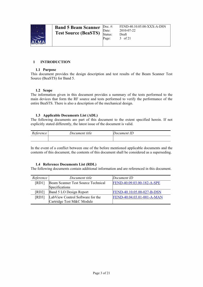
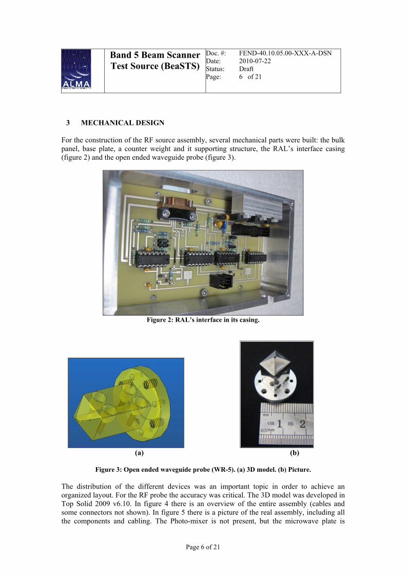
3 MECHANICAL DESIGN For the construction of the RF source assembly, several mechanical parts were built: the bulk panel, base plate, a counter weight and it supporting structure, the RAL’s interface casing (figure 2) and the open ended waveguide probe (figure 3).
Figure 2: RAL’s interface in its casing.
(a) (b)
Figure 3: Open ended waveguide probe (WR-5). (a) 3D model. (b) Picture.
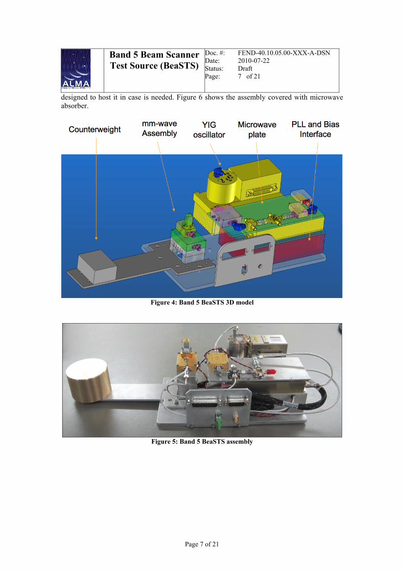
The distribution of the different devices was an important topic in order to achieve an organized layout. For the RF probe the accuracy was critical. The 3D model was developed in Top Solid 2009 v6.10. In figure 4 there is an overview of the entire assembly (cables and some connectors not shown). In figure 5 there is a picture of the real assembly, including all the components and cabling. The Photo-mixer is not present, but the microwave plate is
Page 6 of 21
Band 5 Beam Scanner Test Source (BeaSTS)
Doc. #: FEND-40.10.05.00-XXX-A-DSN Date: 2010-07-22 Status: Draft Page: 7 of 21
designed to host it in case is needed. Figure 6 shows the assembly covered with microwave absorber.
Figure 4: Band 5 BeaSTS 3D model
Figure 5: Band 5 BeaSTS assembly
Page 7 of 21

Band 5 Beam Scanner Test Source (BeaSTS)
Doc. #: FEND-40.10.05.00-XXX-A-DSN Date: 2010-07-22 Status: Draft Page: 8 of 21
Figure 6: Band 5 BeaSTS assembly covered with absorber.
Page 8 of 21
Band 5 Beam Scanner Test Source (BeaSTS)
Doc. #: FEND-40.10.05.00-XXX-A-DSN Date: 2010-07-22 Status: Draft Page: 9 of 21
Page 9 of 21
4 PERFORMANCE TESTS
4.1 Single devices tests Before to assembly the source every device was tested separately. Results are shown in this chapter.
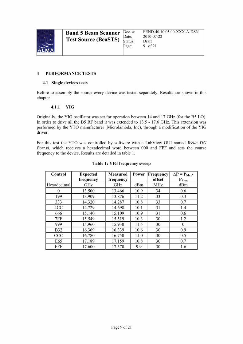
4.1.1 YIG Originally, the YIG oscillator was set for operation between 14 and 17 GHz (for the B5 LO). In order to drive all the B5 RF band it was extended to 13.5 - 17.6 GHz. This extension was performed by the YTO manufacturer (Microlambda, Inc), through a modification of the YIG driver. For this test the YTO was controlled by software with a LabView GUI named Write YIG Port.vi, which receives a hexadecimal word between 000 and FFF and sets the coarse frequency to the device. Results are detailed in table 1.
Table 1: YIG frequency sweep
Control Expected frequency
Measured frequency
Power Frequency offset
∆P = PMax- PFreq
Hexadecimal GHz GHz dBm MHz dBm 0 13.500 13.466 10.9 34 0.6
199 13.909 13.876 11.2 33 0.3 333 14.320 14.287 10.8 33 0.7 4CC 14.729 14.698 10.1 31 1.4 666 15.140 15.109 10.9 31 0.6 7FF 15.549 15.519 10.3 30 1.2 999 15.960 15.930 11.5 30 0 B32 16.369 16.339 10.6 30 0.9 CCC 16.780 16.750 11.0 30 0.5 E65 17.189 17.159 10.8 30 0.7 FFF 17.600 17.570 9.9 30 1.6

Band 5 Beam Scanner Test Source (BeaSTS)
Doc. #: FEND-40.10.05.00-XXX-A-DSN Date: 2010-07-22 Status: Draft Page: 10 of 21
Figure 7: YTO Output power
4.1.2 Quinstar Doubler A 10 dBm input signal was supplied to the Quinstar doubler and the output was measured for different frequencies. The instrument was an Agilent E4418B power meter. Results are detailed in table 2.
Table 2: Quinstar doubler output at 10 dB input
Input Frequency
Doubler input power
Doubler output power
GHz dBm dBm 13.50 10.10 20.50 13.91 10.00 21.00 14.32 10.00 20.00 14.73 10.00 20.90 15.14 10.00 20.00 15.55 10.00 19.90 15.96 9.90 20.10 16.37 10.00 >21 16.78 10.10 >21 17.19 10.00 >21 17.60 10.00 >21
Page 10 of 21

Band 5 Beam Scanner Test Source (BeaSTS)
Doc. #: FEND-40.10.05.00-XXX-A-DSN Date: 2010-07-22 Status: Draft Page: 11 of 21
Figure 8: Quinstar doubler output power
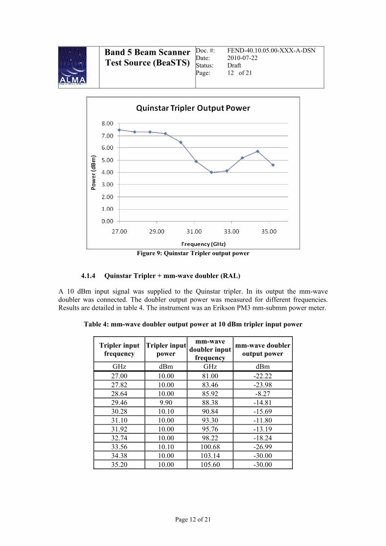
4.1.3 Quinstar Tripler A 10 dBm input signal was supplied to the Quinstar tripler and the total output was measured for different frequencies. Results are detailed in table 3. The instrument was an Erikson PM3millimeter-submillimeter power meter.
Table 3: Quinstar tripler output at 10 dBm input
Input Frequency
Tripler inputpower
Tripler output power
GHz dBm dBm 27.00 10.00 7.48 27.82 10.00 7.32 28.64 10.00 7.32 29.46 9.90 7.19 30.28 10.10 6.48 31.10 10.00 4.90 31.92 10.00 4.01 32.74 10.00 4.13 33.56 10.10 5.19 34.38 10.00 5.72 35.20 10.00 4.61
Page 11 of 21
Band 5 Beam Scanner Test Source (BeaSTS)
Doc. #: FEND-40.10.05.00-XXX-A-DSN Date: 2010-07-22 Status: Draft Page: 12 of 21
Figure 9: Quinstar Tripler output power
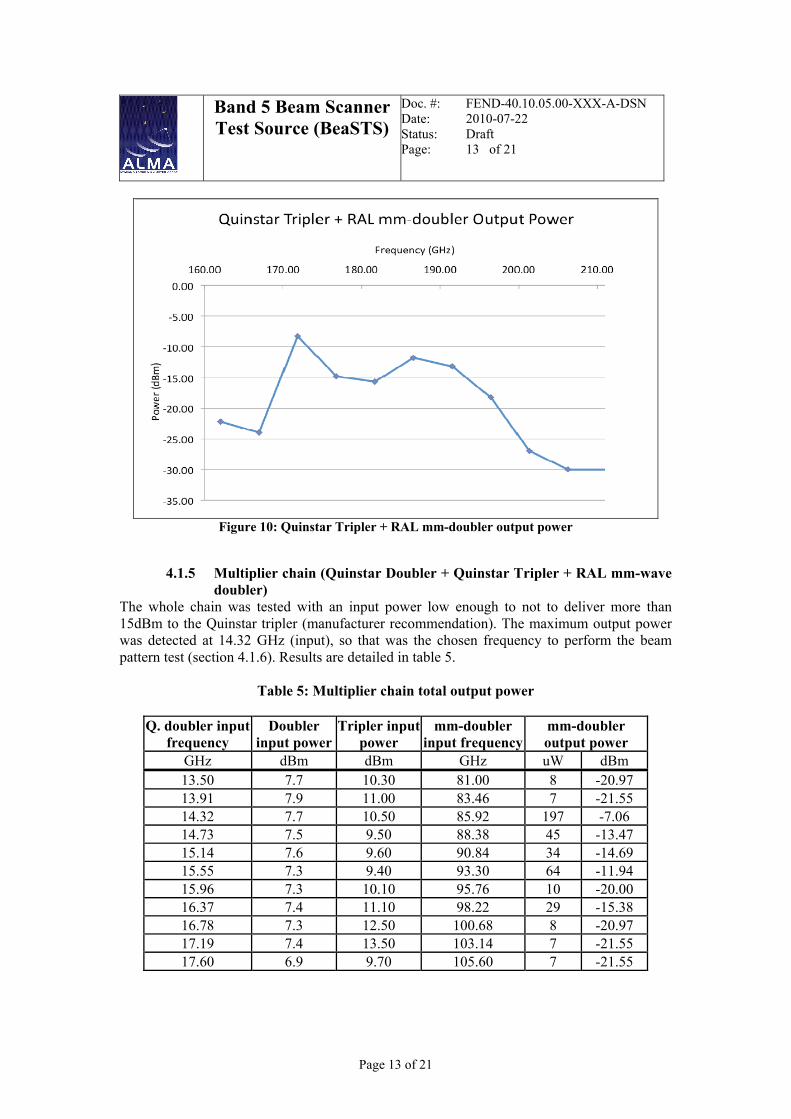
4.1.4 Quinstar Tripler + mm-wave doubler (RAL) A 10 dBm input signal was supplied to the Quinstar tripler. In its output the mm-wave doubler was connected. The doubler output power was measured for different frequencies. Results are detailed in table 4. The instrument was an Erikson PM3 mm-submm power meter.
Table 4: mm-wave doubler output power at 10 dBm tripler input power
Tripler input frequency
Tripler inputpower
mm-wave doubler input
frequency
mm-wave doubler output power
GHz dBm GHz dBm 27.00 10.00 81.00 -22.22 27.82 10.00 83.46 -23.98 28.64 10.00 85.92 -8.27 29.46 9.90 88.38 -14.81 30.28 10.10 90.84 -15.69 31.10 10.00 93.30 -11.80 31.92 10.00 95.76 -13.19 32.74 10.00 98.22 -18.24 33.56 10.10 100.68 -26.99 34.38 10.00 103.14 -30.00 35.20 10.00 105.60 -30.00
Page 12 of 21
Band 5 Beam Scanner Test Source (BeaSTS)
Doc. #: FEND-40.10.05.00-XXX-A-DSN Date: 2010-07-22 Status: Draft Page: 13 of 21
Figure 10: Quinstar Tripler + RAL mm-doubler output power
4.1.5 Multiplier chain (Quinstar Doubler + Quinstar Tripler + RAL mm-wave doubler)
The whole chain was tested with an input power low enough to not to deliver more than 15dBm to the Quinstar tripler (manufacturer recommendation). The maximum output power was detected at 14.32 GHz (input), so that was the chosen frequency to perform the beam pattern test (section 4.1.6). Results are detailed in table 5.
Table 5: Multiplier chain total output power
Q. doubler input frequency
Doubler input power
Tripler inputpower
mm-doubler input frequency
mm-doubler output power
GHz dBm dBm GHz uW dBm 13.50 7.7 10.30 81.00 8 -20.97 13.91 7.9 11.00 83.46 7 -21.55 14.32 7.7 10.50 85.92 197 -7.06 14.73 7.5 9.50 88.38 45 -13.47 15.14 7.6 9.60 90.84 34 -14.69 15.55 7.3 9.40 93.30 64 -11.94 15.96 7.3 10.10 95.76 10 -20.00 16.37 7.4 11.10 98.22 29 -15.38 16.78 7.3 12.50 100.68 8 -20.97 17.19 7.4 13.50 103.14 7 -21.55 17.60 6.9 9.70 105.60 7 -21.55
Page 13 of 21

Band 5 Beam Scanner Test Source (BeaSTS)
Doc. #: FEND-40.10.05.00-XXX-A-DSN Date: 2010-07-22 Status: Draft Page: 14 of 21
Figure 11: Multiplier chain output power
4.1.6 Waveguide Probe Beam Pattern The multiplier chain was mounted on an aluminium structure bolted to a rotary stage. In front of it, a standard gain horn connected to a power meter was used. The complete setup lies on an optic table. The setup is shown in figure 12.
Figure 12: Experimental setup for beam pattern measurement
Page 14 of 21
Band 5 Beam Scanner Test Source (BeaSTS)
Doc. #: FEND-40.10.05.00-XXX-A-DSN Date: 2010-07-22 Status: Draft Page: 15 of 21
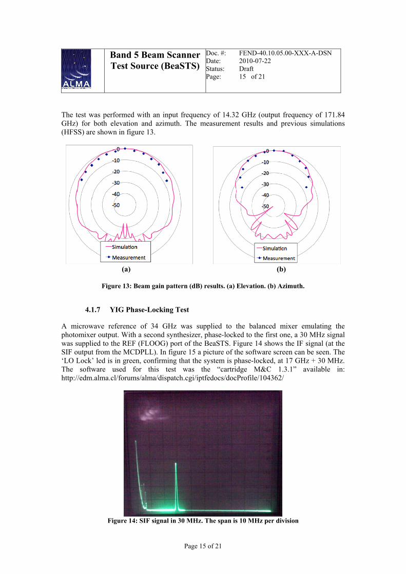
The test was performed with an input frequency of 14.32 GHz (output frequency of 171.84 GHz) for both elevation and azimuth. The measurement results and previous simulations (HFSS) are shown in figure 13.
(a) (b)
Figure 13: Beam gain pattern (dB) results. (a) Elevation. (b) Azimuth.
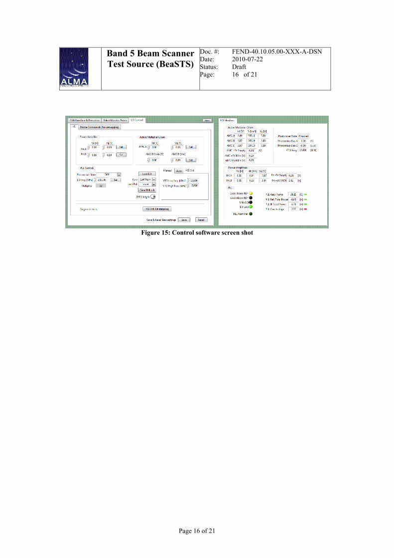
4.1.7 YIG Phase-Locking Test A microwave reference of 34 GHz was supplied to the balanced mixer emulating the photomixer output. With a second synthesizer, phase-locked to the first one, a 30 MHz signal was supplied to the REF (FLOOG) port of the BeaSTS. Figure 14 shows the IF signal (at the SIF output from the MCDPLL). In figure 15 a picture of the software screen can be seen. The ‘LO Lock’ led is in green, confirming that the system is phase-locked, at 17 GHz + 30 MHz. The software used for this test was the “cartridge M&C 1.3.1” available in: http://edm.alma.cl/forums/alma/dispatch.cgi/iptfedocs/docProfile/104362/
Figure 14: SIF signal in 30 MHz. The span is 10 MHz per division
Page 15 of 21
Band 5 Beam Scanner Test Source (BeaSTS)
Doc. #: FEND-40.10.05.00-XXX-A-DSN Date: 2010-07-22 Status: Draft Page: 16 of 21
Figure 15: Control software screen shot
Page 16 of 21

Band 5 Beam Scanner Test Source (BeaSTS)
Doc. #: FEND-40.10.05.00-XXX-A-DSN Date: 2010-07-22 Status: Draft Page: 17 of 21
Page 17 of 21
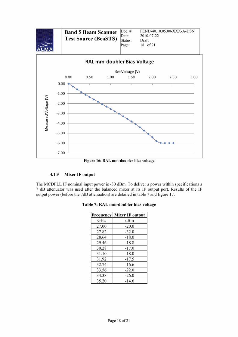
4.1.8 RAL mm-doubler Bias Voltage The RAL mm-doubler has a bias voltage range of 0 to -6V. To set this voltage the PA B Vd port is used. The software (originally design for NRAO’s PA) presents a scaling issue. The Bias interface sets a voltage equal to aprox. -2.6 times the voltage commanded at the software. The voltage output is limited by hardware by the bias interface so no danger for overvoltage is present. The bias voltage delivered to the mm-wave doubler was characterized for different set voltages on the software. Results are detailed in table 6.
Table 6: RAL mm-doubler bias voltage
Set Voltage
Monitor Voltage
Measured Voltage
V V V 0.0 0.01 0.00 0.1 -0.29 -0.29 0.2 -0.57 -0.57 0.3 -0.85 -0.86 0.4 -1.11 -1.11 0.5 -1.35 -1.35 0.6 -1.59 -1.59 0.7 -1.82 -1.83 0.8 -2.08 -2.08 0.9 -2.31 -2.31 1.0 -2.54 -2.55 1.1 -2.78 -2.79 1.2 -3.02 -3.03 1.3 -3.29 -3.29 1.4 -3.55 -3.55 1.5 -3.81 -3.82 1.6 -4.09 -4.10 1.7 -4.39 -4.40 1.8 -4.73 -4.74 1.9 -4.98 -5.07 2.0 -4.98 -5.42 2.1 -4.98 -5.81 2.2 -4.98 -5.99 2.3 -4.98 -6.00 2.4 -4.98 -6.00 2.5 -4.98 -6.00
Band 5 Beam Scanner Test Source (BeaSTS)
Doc. #: FEND-40.10.05.00-XXX-A-DSN Date: 2010-07-22 Status: Draft Page: 18 of 21
Page 18 of 21
Figure 16: RAL mm-doubler bias voltage
4.1.9 Mixer IF output The MCDPLL IF nominal input power is -30 dBm. To deliver a power within specifications a 7 dB attenuator was used after the balanced mixer at its IF output port. Results of the IF output power (before the 7dB attenuation) are detailed in table 7 and figure 17.
Table 7: RAL mm-doubler bias voltage
Frequency Mixer IF output
GHz dBm 27.00 -20.0 27.82 -32.0 28.64 -18.0 29.46 -18.8 30.28 -17.0 31.10 -18.0 31.92 -17.5 32.74 -16.6 33.56 -22.0 34.38 -26.0 35.20 -14.6

Band 5 Beam Scanner Test Source (BeaSTS)
Doc. #: FEND-40.10.05.00-XXX-A-DSN Date: 2010-07-22 Status: Draft Page: 19 of 21
Figure 17: Mixer IF output power
Page 19 of 21

Band 5 Beam Scanner Test Source (BeaSTS)
Doc. #: FEND-40.10.05.00-XXX-A-DSN Date: 2010-07-22 Status: Draft Page: 20 of 21
Page 20 of 21
4.2 Overall source tests
4.2.1 Total Output Power Using the configuration shown in figure 1, with the BeaSTS totally assembled, the total output power was measured using an Erickson mm-submm power meter (figure 19). The source was phase-locked for each frequency. For that purpose the photo-mixer input was connected to an Agilent E8257D synthesizer, which provided a 27 to 35.2 GHz signal to the balanced mixer. The 30 MHz FLOOG reference was provided by an Agilent N5181 signal generator phase-locked to the later. Total output power was measured at each frequency for different values of RAL’s mm-wave doubler bias voltage, which gives different levels of attenuation. Blank fields represent levels below the instrument detection threshold. Results are shown table 8 and figure 18.
Table 8: BeaSTS total output power (locked)
PA B Vd = 0 V
PA B Vd = 0.5
PA B Vd = 1.0 V
PA B Vd = 1.5 V
PA B Vd = 2.0 V
PA B Vd = 2.5 V
Frequency Output Power GHz uW uW uW uW uW uW
162.00 6.60 1.07 0.31 166.92 4.20 0.60 0.10 171.84 147.00 38.00 17.50 7.50 2.50 2.00 176.76 39.00 10.50 4.60 181.68 39.40 14.90 7.90 4.00 2.15 1.80 186.60 84.50 23.70 10.65 4.32 1.66 1.35 191.52 5.30 0.75 0.20 196.44 24.80 9.50 4.70 2.30 1.20 1.00 201.36 1.75 0.40 206.28 211.20

Band 5 Beam Scanner Test Source (BeaSTS)
Doc. #: FEND-40.10.05.00-XXX-A-DSN Date: 2010-07-22 Status: Draft Page: 21 of 21
Pow
er(u
W)
Pow
er(u
W)
Figure 18: BeaSTS total output power for 3 different attenuation levels (PA B Vd)
Figure 19: Total power measurement. Power meter connected to the output of the BeaSTS
Page 21 of 21