Embed Size (px)
Citation preview
CDCM61002
www.ti.com SCAS870F –FEBRUARY 2009–REVISED JUNE 2011
Two Output, Integrated VCO, Low-Jitter Clock GeneratorCheck for Samples: CDCM61002
• Divider Programming Using Control Pins:1FEATURES
– Two Pins for Prescaler/Feedback Divider2• One Crystal/LVCMOS Reference Input
– Three Pins for Output DividerIncluding 24.8832 MHz, 25 MHz, and26.5625 MHz – Two Pins for Output Select
• Input Frequency Range: 21.875 MHz to • Chip Enable Control Pin Available28.47 MHz • 3.3-V Core and I/O Power Supply
• On-Chip VCO Operates in Frequency Range of • Industrial Temperature Range: –40°C to +85°C1.75 GHz to 2.05 GHz
• 5-mm × 5-mm, 32-pin, QFN (RHB) Package• 2x Output Available:• ESD Protection Exceeds 2 kV (HBM)– Pin-Selectable Between LVPECL, LVDS, or
2-LVCMOS; Operates at 3.3 V APPLICATIONS• LVCMOS Bypass Output Available
• Low Jitter Clock Driver for High-End Datacom• Output Frequency Selectable by /1, /2, /3, /4, /6, Applications Including SONET, Ethernet, Fibre/8 from a Single Output Divider Channel, Serial ATA, and HDTV• Supports Common LVPECL/LVDS Output • Cost-Effective High-Frequency CrystalFrequencies: Oscillator Replacement
– 62.5 MHz, 74.25 MHz, 75 MHz, 77.76 MHz,100 MHz, 106.25 MHz, 125 MHz, 150 MHz,155.52 MHz, 156.25 MHz, 159.375 MHz,
DESCRIPTION187.5 MHz, 200 MHz, 212.5 MHz, 250 MHz,The CDCM61002 is a highly versatile, low-jitter311.04 MHz, 312.5 MHz, 622.08 MHz,frequency synthesizer that can generate two low-jitter625 MHzclock outputs, selectable between low-voltage• Supports Common LVCMOS Outputpositive emitter coupled logic (LVPECL), low-voltageFrequencies:differential signaling (LVDS), or low-voltage– 62.5 MHz, 74.25 MHz, 75 MHz, 77.76 MHz, complementary metal oxide semiconductor100 MHz, 106.25 MHz, 125 MHz, 150 MHz, (LVCMOS) outputs, from a low-frequency crystal or155.52 MHz, 156.25 MHz, 159.375 MHz, LVCMOS input for a variety of wireline and data187.5 MHz, 200 MHz, 212.5 MHz, 250 MHz communication applications. The CDCM61002
• Output Frequency Range: 43.75 MHz to features an onboard PLL that can be easily683.264 MHz (See Table 3) configured solely through control pins. The overall
• Internal PLL Loop Bandwidth: 400 kHz output random jitter performance is less than 1ps,RMS (from 10 kHz to 20 MHz), making this device a• High-Performance PLL Core:perfect choice for use in demanding applications such– Phase Noise typically at –146 dBc/Hz atas SONET, Ethernet, Fibre Channel, and SAN. The5-MHz Offset for 625-MHz LVPECL OutputCDCM61002 is available in a small, 32-pin, 5-mm ×– Random Jitter typically at 0.509 ps, RMS 5-mm QFN package.
(10 kHz to 20 MHz) for 625-MHz LVPECLOutput
• Output Duty Cycle Corrected to 50% (± 5%)• Low Output Skew of 20 ps on LVPECL Outputs
1
Please be aware that an important notice concerning availability, standard warranty, and use in critical applications of TexasInstruments semiconductor products and disclaimers thereto appears at the end of this data sheet.
2All trademarks are the property of their respective owners.
PRODUCTION DATA information is current as of publication date. Copyright © 2009–2011, Texas Instruments IncorporatedProducts conform to specifications per the terms of the TexasInstruments standard warranty. Production processing does notnecessarily include testing of all parameters.
f =IN
Output Divider
Feedback Divider( (fOUT
PFDCharge Pump
Loop Filter
FeedbackDivider
Pre
scale
r
Outp
ut D
ivid
er
CE
LVPECL/LVCMOS/LVDS
LVPECL/LVCMOS/LVDS
OS[1...0]
OD[2...0]PR[1...0]
2
2 3
RSTN
VCO
3.3 V
CDCM61002
Crystal/LVCMOS
OutputDriver
OutputDriver
LVCMOS
CDCM61002
SCAS870F –FEBRUARY 2009–REVISED JUNE 2011 www.ti.com
This integrated circuit can be damaged by ESD. Texas Instruments recommends that all integrated circuits be handled withappropriate precautions. Failure to observe proper handling and installation procedures can cause damage.
ESD damage can range from subtle performance degradation to complete device failure. Precision integrated circuits may be moresusceptible to damage because very small parametric changes could cause the device not to meet its published specifications.
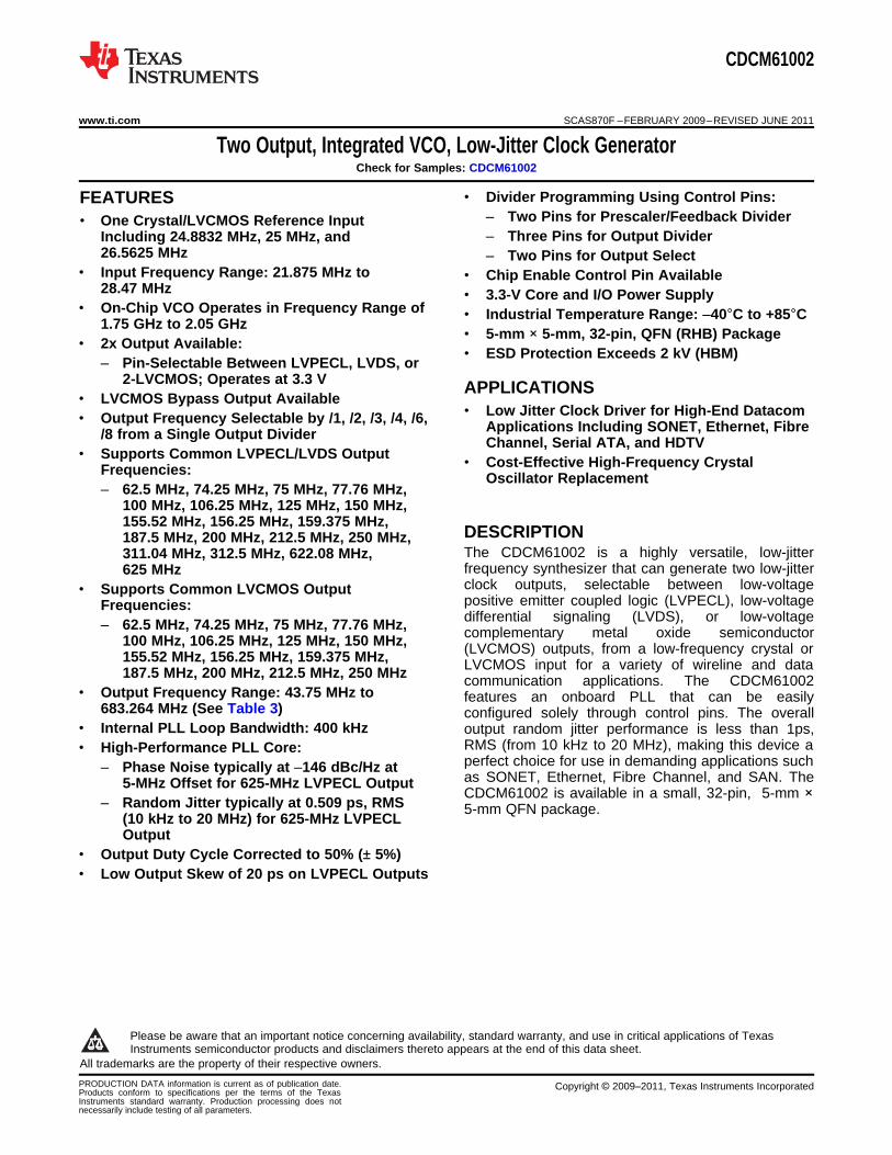
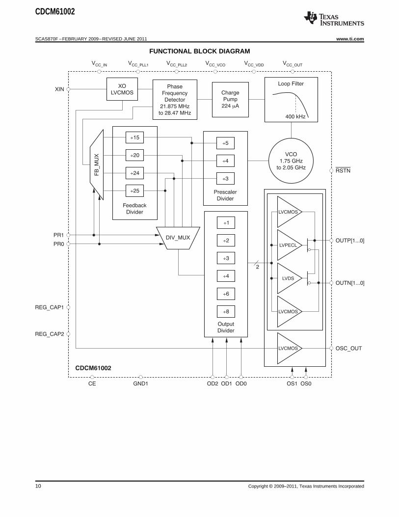
DESCRIPTION, CONTINUEDThe CDCM61002 is a high-performance, low phase noise, fully-integrated voltage-controlled oscillator (VCO)clock synthesizer with two universal output buffers that can be configured to be LVPECL, LVDS, or LVCMOScompatible. Each universal output can also be converted to two LVCMOS outputs. Additionally, an LVCMOSbypass output clock is available in an output configuration which can help with crystal loading in order to achievean exact desired input frequency. It has one fully-integrated, low-noise, LC-based VCO that operates in the 1.75GHz to 2.05 GHz range.
The phase-locked loop (PLL) synchronizes the VCO with respect to the input, which can either be alow-frequency crystal. The outputs share an output divider sourced from the VCO core. All device settings aremanaged through a control pin structure, which has two pins that control the prescaler and feedback divider,three pins that control the output divider, two pins that control the output type, and one pin that controls theoutput enable. Any time the PLL settings (including the input frequency, prescaler divider, or feedback divider)are altered, a reset must be issued through the Reset control pin (active low for device reset). The reset initiatesa PLL recalibration process to ensure PLL lock. When the device is in reset, the outputs and dividered are turnedoff.
The output frequency (fOUT) is proportional to the frequency of the input clock (fIN). The feedback divider, outputdivider, and VCO frequency set fOUT with respect to fIN. For a configuration setting for common wireline anddatacom applications, refer toTable 2. For other applications, use Equation 1 to calculate the exact crystaloscillator frequency required for the desired output.
(1)
The output divider can be chosen from 1, 2, 3, 4, 6, or 8 through the use of control pins. Feedback divider andprescaler divider combinations can be chosen from 25 and 3, 24 and 3, 20 and 4, or 15 and 5, respectively, alsothrough the use of control pins. Figure 1 shows a high-level block diagram of the CDCM61002.
The device operates in a 3.3-V supply environment and is characterized for operation from –40°C to +85°C.
Figure 1. CDCM61002 Block Diagram
2 Copyright © 2009–2011, Texas Instruments Incorporated
CDCM61002
www.ti.com SCAS870F –FEBRUARY 2009–REVISED JUNE 2011
AVAILABLE OPTIONS (1)
TA PACKAGED DEVICES FEATURES (2)
CDCM61002RHBT 32-pin QFN (RHB) package, small tape and reel–40°C to +85°C
CDCM61002RHBR 32-pin QFN (RHB) package, tape and reel
(1) For the most current specifications and package information, see the Package Option Addendum located at the end of this data sheet orrefer to our web site at www.ti.com.
(2) These packages conform to Lead (Pb)-free and green manufacturing specifications. Additional details including specific materialcontentcan be accessed at www.ti.com/leadfree. GREEN: TI defines Green to mean Lead (Pb)-Free and in addition, uses less packagematerials that do not contain halogens, including bromine (Br), or antimony (Sb) above 0.1%of total product weight. N/A: Not yetavailable Lead (Pb)-Free; for estimated conversion dates, go to www.ti.com/leadfree. Pb-FREE: TI defines Lead (Pb)-Free to meanRoHS compatible, including a lead concentration that does not exceed 0.1% of total product weight, and, if designed to be soldered,suitable for use in specified lead-free soldering processes.
ABSOLUTE MAXIMUM RATINGS (1)
Over operating free-air temperature range (unless otherwise noted).
PARAMETER VALUE UNIT
VCC_OUT,VCC_PLL1,VCC_PLL2, Supply voltage range (2) –0.5 to 4.6 VVCC_VCO,VCC_IN
VIN Input voltage range (3) –0.5 to (VCC_IN + 0.5) V
VOUT Output voltage range (3) –0.5 to (VCC_OUT + 0.5) V
IIN Input current 20 mA
IOUT Output current 50 mA
TSTG Storage temperature range –65 to +150 °C
(1) Stresses beyond those listed under absolute maximum ratings may cause permanent damage to the device. These are stress ratingsonly, and functional operation of the device at these or any other conditions beyond those indicated under recommended operatingcondition is not implied. Exposure to absolute-maximum-rated conditions for extended periods may affect device reliability.
(2) All supply voltages must be supplied simultaneously.(3) Input and output negative voltage ratings may be exceeded if the input and output clamp-current ratings are observed.
RECOMMENDED OPERATING CONDITIONSOver operating free-air temperature range (unless otherwise noted).
PARAMETER MIN NOM MAX UNIT
VCC_OUT Output supply voltage 3.0 3.30 3.60 V
VCC_PLL1 PLL supply voltage 3.0 3.30 3.60 V
VCC_PLL2 PLL supply voltage 3.0 3.30 3.60 V
VCC_VCO On-chip VCO supply voltage 3.0 3.30 3.60 V
VCC_IN Input supply voltage 3.0 3.30 3.60 V
TA Ambient temperature –40 +85 °C
DISSIPATION RATINGS (1) (2)
VALUE
TEST 4 × 4 VIASPARAMETER CONDITIONS ON PAD UNIT
θJA Thermal resistance, junction-to-ambient 0 LFM 35 °C/W
θJP(3) Thermal resistance, junction-to-pad 4 °C/W
(1) The package thermal resistance is calculated in accordance with JESD 51 and JEDEC 2S2P (high-K board).(2) Connected to GND with nine thermal vias (0.3-mm diameter).(3) θJP (junction-to-pad) is used for the QFN package, because the primary heat flow is from the junction to the GND pad of the QFN
package.
Copyright © 2009–2011, Texas Instruments Incorporated 3
CDCM61002
SCAS870F –FEBRUARY 2009–REVISED JUNE 2011 www.ti.com
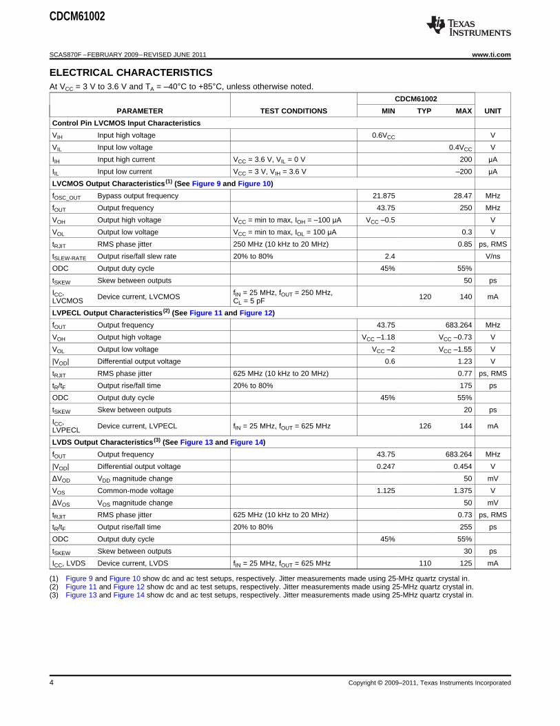
ELECTRICAL CHARACTERISTICSAt VCC = 3 V to 3.6 V and TA = –40°C to +85°C, unless otherwise noted.
CDCM61002
PARAMETER TEST CONDITIONS MIN TYP MAX UNIT
Control Pin LVCMOS Input Characteristics
VIH Input high voltage 0.6VCC V
VIL Input low voltage 0.4VCC V
IIH Input high current VCC = 3.6 V, VIL = 0 V 200 μA
IIL Input low current VCC = 3 V, VIH = 3.6 V –200 μA
LVCMOS Output Characteristics (1) (See Figure 9 and Figure 10)
fOSC_OUT Bypass output frequency 21.875 28.47 MHz
fOUT Output frequency 43.75 250 MHz
VOH Output high voltage VCC = min to max, IOH = –100 μA VCC –0.5 V
VOL Output low voltage VCC = min to max, IOL = 100 μA 0.3 V
tRJIT RMS phase jitter 250 MHz (10 kHz to 20 MHz) 0.85 ps, RMS
tSLEW-RATE Output rise/fall slew rate 20% to 80% 2.4 V/ns
ODC Output duty cycle 45% 55%
tSKEW Skew between outputs 50 ps
ICC, fIN = 25 MHz, fOUT = 250 MHz,Device current, LVCMOS 120 140 mALVCMOS CL = 5 pF
LVPECL Output Characteristics (2) (See Figure 11 and Figure 12)
fOUT Output frequency 43.75 683.264 MHz
VOH Output high voltage VCC –1.18 VCC –0.73 V
VOL Output low voltage VCC –2 VCC –1.55 V
|VOD| Differential output voltage 0.6 1.23 V
tRJIT RMS phase jitter 625 MHz (10 kHz to 20 MHz) 0.77 ps, RMS
tR/tF Output rise/fall time 20% to 80% 175 ps
ODC Output duty cycle 45% 55%
tSKEW Skew between outputs 20 ps
ICC, Device current, LVPECL fIN = 25 MHz, fOUT = 625 MHz 126 144 mALVPECL
LVDS Output Characteristics (3) (See Figure 13 and Figure 14)
fOUT Output frequency 43.75 683.264 MHz
|VOD| Differential output voltage 0.247 0.454 V
ΔVOD VDD magnitude change 50 mV
VOS Common-mode voltage 1.125 1.375 V
ΔVOS VOS magnitude change 50 mV
tRJIT RMS phase jitter 625 MHz (10 kHz to 20 MHz) 0.73 ps, RMS
tR/tF Output rise/fall time 20% to 80% 255 ps
ODC Output duty cycle 45% 55%
tSKEW Skew between outputs 30 ps
ICC, LVDS Device current, LVDS fIN = 25 MHz, fOUT = 625 MHz 110 125 mA
(1) Figure 9 and Figure 10 show dc and ac test setups, respectively. Jitter measurements made using 25-MHz quartz crystal in.(2) Figure 11 and Figure 12 show dc and ac test setups, respectively. Jitter measurements made using 25-MHz quartz crystal in.(3) Figure 13 and Figure 14 show dc and ac test setups, respectively. Jitter measurements made using 25-MHz quartz crystal in.
4 Copyright © 2009–2011, Texas Instruments Incorporated
CDCM61002
www.ti.com SCAS870F –FEBRUARY 2009–REVISED JUNE 2011
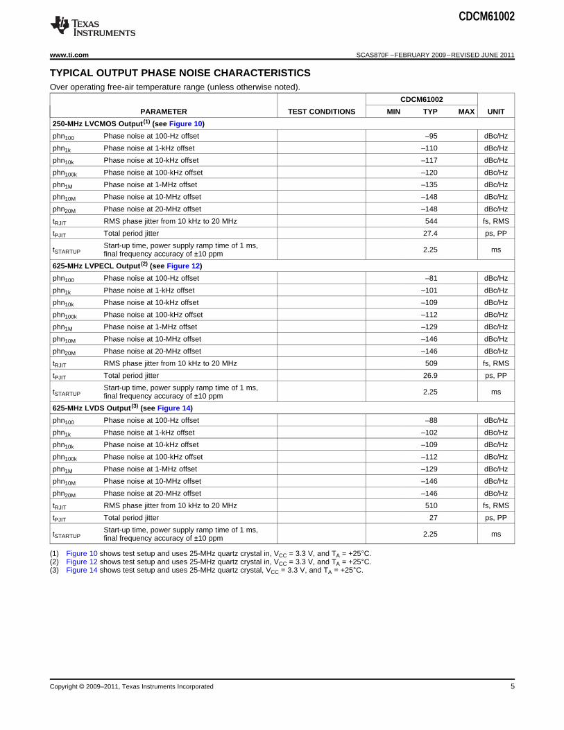
TYPICAL OUTPUT PHASE NOISE CHARACTERISTICSOver operating free-air temperature range (unless otherwise noted).
CDCM61002
PARAMETER TEST CONDITIONS MIN TYP MAX UNIT
250-MHz LVCMOS Output (1) (see Figure 10)
phn100 Phase noise at 100-Hz offset –95 dBc/Hz
phn1k Phase noise at 1-kHz offset –110 dBc/Hz
phn10k Phase noise at 10-kHz offset –117 dBc/Hz
phn100k Phase noise at 100-kHz offset –120 dBc/Hz
phn1M Phase noise at 1-MHz offset –135 dBc/Hz
phn10M Phase noise at 10-MHz offset –148 dBc/Hz
phn20M Phase noise at 20-MHz offset –148 dBc/Hz
tRJIT RMS phase jitter from 10 kHz to 20 MHz 544 fs, RMS
tPJIT Total period jitter 27.4 ps, PP
Start-up time, power supply ramp time of 1 ms,tSTARTUP 2.25 msfinal frequency accuracy of ±10 ppm
625-MHz LVPECL Output (2) (see Figure 12)
phn100 Phase noise at 100-Hz offset –81 dBc/Hz
phn1k Phase noise at 1-kHz offset –101 dBc/Hz
phn10k Phase noise at 10-kHz offset –109 dBc/Hz
phn100k Phase noise at 100-kHz offset –112 dBc/Hz
phn1M Phase noise at 1-MHz offset –129 dBc/Hz
phn10M Phase noise at 10-MHz offset –146 dBc/Hz
phn20M Phase noise at 20-MHz offset –146 dBc/Hz
tRJIT RMS phase jitter from 10 kHz to 20 MHz 509 fs, RMS
tPJIT Total period jitter 26.9 ps, PP
Start-up time, power supply ramp time of 1 ms,tSTARTUP 2.25 msfinal frequency accuracy of ±10 ppm
625-MHz LVDS Output (3) (see Figure 14)
phn100 Phase noise at 100-Hz offset –88 dBc/Hz
phn1k Phase noise at 1-kHz offset –102 dBc/Hz
phn10k Phase noise at 10-kHz offset –109 dBc/Hz
phn100k Phase noise at 100-kHz offset –112 dBc/Hz
phn1M Phase noise at 1-MHz offset –129 dBc/Hz
phn10M Phase noise at 10-MHz offset –146 dBc/Hz
phn20M Phase noise at 20-MHz offset –146 dBc/Hz
tRJIT RMS phase jitter from 10 kHz to 20 MHz 510 fs, RMS
tPJIT Total period jitter 27 ps, PP
Start-up time, power supply ramp time of 1 ms,tSTARTUP 2.25 msfinal frequency accuracy of ±10 ppm
(1) Figure 10 shows test setup and uses 25-MHz quartz crystal in, VCC = 3.3 V, and TA = +25°C.(2) Figure 12 shows test setup and uses 25-MHz quartz crystal in, VCC = 3.3 V, and TA = +25°C.(3) Figure 14 shows test setup and uses 25-MHz quartz crystal, VCC = 3.3 V, and TA = +25°C.
Copyright © 2009–2011, Texas Instruments Incorporated 5
CDCM61002
SCAS870F –FEBRUARY 2009–REVISED JUNE 2011 www.ti.com
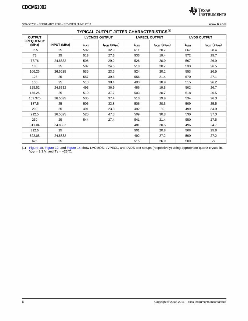
TYPICAL OUTPUT JITTER CHARACTERISTICS (1)
OUTPUT LVCMOS OUTPUT LVPECL OUTPUT LVDS OUTPUTFREQUENCY
(MHz) INPUT (MHz) tRJIT tPJIT (psPP) tRJIT tPJIT (psPP) tRJIT tPJIT (psPP)
62.5 25 592 32.9 611 20.7 667 28.4
75 25 518 27.5 533 19.4 572 25.7
77.76 24.8832 506 29.2 526 20.9 567 26.9
100 25 507 24.5 510 20.7 533 26.5
106.25 26.5625 535 23.5 524 20.2 553 26.5
125 25 557 39.6 556 21.4 570 27.1
150 25 518 38.4 493 18.9 515 26.2
155.52 24.8832 498 36.9 486 19.8 502 26.7
156.25 25 510 37.7 503 20.7 518 26.5
159.375 26.5625 535 37.4 510 19.9 534 26.3
187.5 25 506 32.8 506 20.3 509 25.5
200 25 491 23.3 492 30 499 34.9
212.5 26.5625 520 47.8 509 30.8 530 37.3
250 25 544 27.4 541 21.4 550 27.5
311.04 24.8832 481 20.5 496 24.7
312.5 25 501 20.8 508 25.8
622.08 24.8832 492 27.2 500 27.2
625 25 515 26.9 509 27
(1) Figure 10, Figure 12, and Figure 14 show LVCMOS, LVPECL, and LVDS test setups (respectively) using appropriate quartz crystal in,VCC = 3.3 V, and TA = +25°C.
6 Copyright © 2009–2011, Texas Instruments Incorporated
NCV _OUTCC
OUTN1
V _OUTCC
V_V
CO
CC
NC
V_P
LL2
CC
PR
0
NC
OUTP1
1
2
3
4
5
6
7
8
24
23
22
21
20
19
18
17
CDCM61002
32 31 30 29 28 27 26 25
9
Thermal Pad
(must be soldered to ground)
10 11 12 13 14 15 16
OUTN0
OUTP0
CE
OS
1N
C
OS
0N
C
RS
TN
NC
OD
0N
C
OD
1N
C
OD
2P
R1
OSC_OUT
GND1
XIN
V _INCC
REG_CAP1
V _PLL1CC
REG_CAP2
CDCM61002
www.ti.com SCAS870F –FEBRUARY 2009–REVISED JUNE 2011
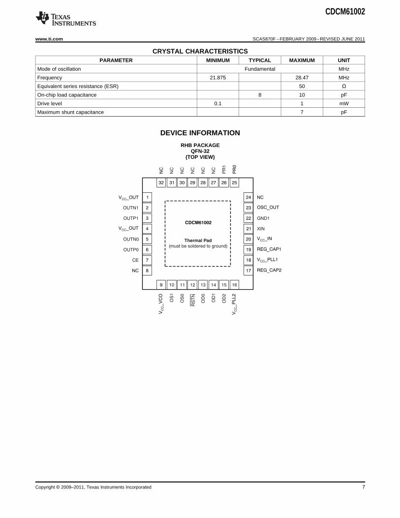
CRYSTAL CHARACTERISTICSPARAMETER MINIMUM TYPICAL MAXIMUM UNIT
Mode of oscillation Fundamental MHz
Frequency 21.875 28.47 MHz
Equivalent series resistance (ESR) 50 ΩOn-chip load capacitance 8 10 pF
Drive level 0.1 1 mW
Maximum shunt capacitance 7 pF
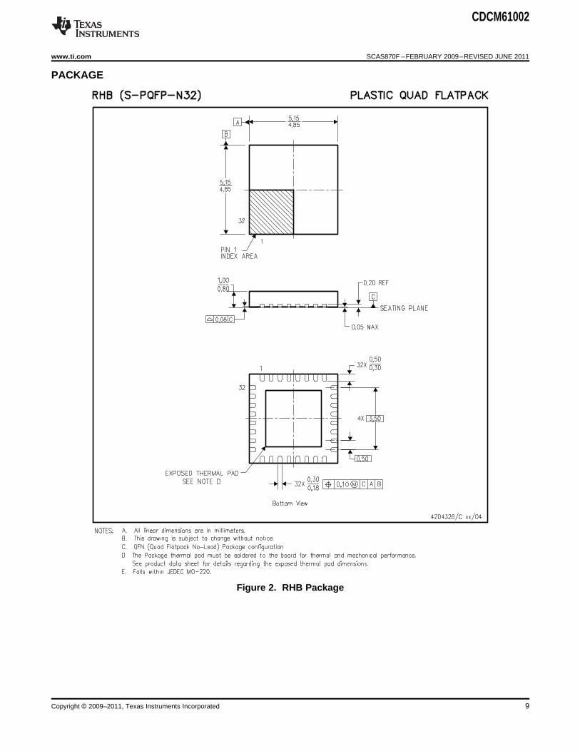
DEVICE INFORMATION
RHB PACKAGEQFN-32
(TOP VIEW)
Copyright © 2009–2011, Texas Instruments Incorporated 7
CDCM61002
SCAS870F –FEBRUARY 2009–REVISED JUNE 2011 www.ti.com
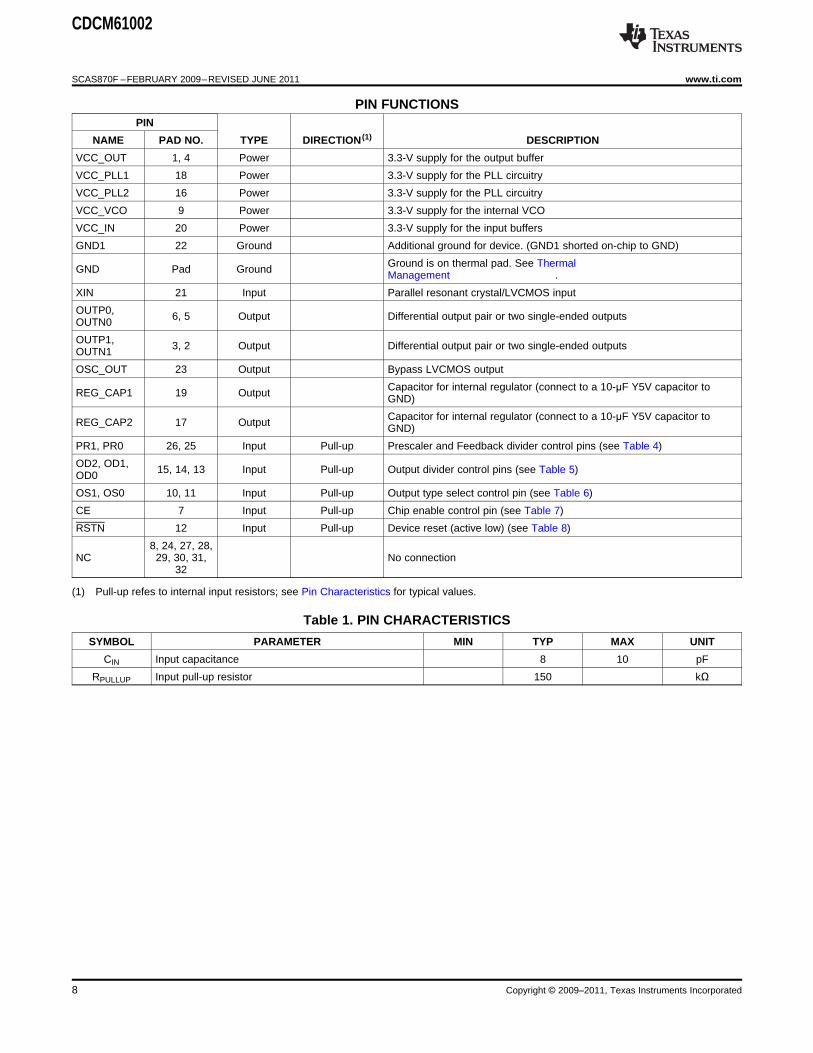
PIN FUNCTIONSPIN
NAME PAD NO. TYPE DIRECTION (1) DESCRIPTION
VCC_OUT 1, 4 Power 3.3-V supply for the output buffer
VCC_PLL1 18 Power 3.3-V supply for the PLL circuitry
VCC_PLL2 16 Power 3.3-V supply for the PLL circuitry
VCC_VCO 9 Power 3.3-V supply for the internal VCO
VCC_IN 20 Power 3.3-V supply for the input buffers
GND1 22 Ground Additional ground for device. (GND1 shorted on-chip to GND)
Ground is on thermal pad. See ThermalGND Pad Ground Management .
XIN 21 Input Parallel resonant crystal/LVCMOS input
OUTP0, 6, 5 Output Differential output pair or two single-ended outputsOUTN0
OUTP1, 3, 2 Output Differential output pair or two single-ended outputsOUTN1
OSC_OUT 23 Output Bypass LVCMOS output
Capacitor for internal regulator (connect to a 10-μF Y5V capacitor toREG_CAP1 19 Output GND)
Capacitor for internal regulator (connect to a 10-μF Y5V capacitor toREG_CAP2 17 Output GND)
PR1, PR0 26, 25 Input Pull-up Prescaler and Feedback divider control pins (see Table 4)
OD2, OD1, 15, 14, 13 Input Pull-up Output divider control pins (see Table 5)OD0
OS1, OS0 10, 11 Input Pull-up Output type select control pin (see Table 6)
CE 7 Input Pull-up Chip enable control pin (see Table 7)
RSTN 12 Input Pull-up Device reset (active low) (see Table 8)
8, 24, 27, 28,NC 29, 30, 31, No connection
32
(1) Pull-up refes to internal input resistors; see Pin Characteristics for typical values.
Table 1. PIN CHARACTERISTICS
SYMBOL PARAMETER MIN TYP MAX UNIT
CIN Input capacitance 8 10 pF
RPULLUP Input pull-up resistor 150 kΩ
8 Copyright © 2009–2011, Texas Instruments Incorporated
CDCM61002
www.ti.com SCAS870F –FEBRUARY 2009–REVISED JUNE 2011
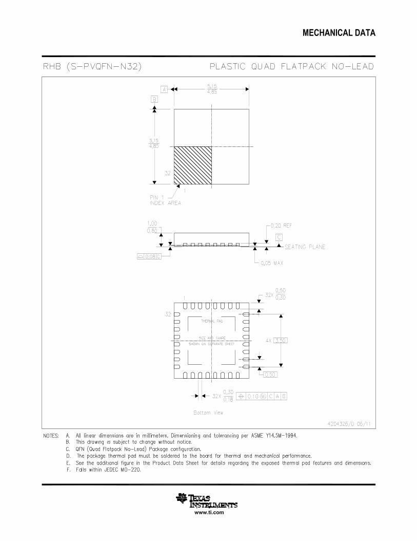
PACKAGE
Figure 2. RHB Package
Copyright © 2009–2011, Texas Instruments Incorporated 9
ChargePump
224 Am
PhaseFrequencyDetector
21.875 MHzto 28.47 MHz
XOLVCMOS
Loop Filter
400 kHz
¸15
¸20
¸24
¸25
FeedbackDivider
¸1
¸2
¸3
¸4
¸6
¸8
OutputDivider
¸5
¸4
¸3
PrescalerDivider
FB
_M
UX
DIV_MUX
VCO1.75 GHz
to 2.05 GHz
PR1
XIN
VCC_IN
CE GND1
RSTN
OUTP[1...0]
OUTN[1...0]
OSC_OUT
OD2 OD1 OD0 OS1 OS0
VCC_PLL1 VCC_PLL2 VCC_VDDVCC_VCO VCC_OUT
PR0
REG_CAP1
REG_CAP2
2
LVCMOS
LVPECL
LVDS
LVCMOS
LVCMOS
CDCM61002
CDCM61002
SCAS870F –FEBRUARY 2009–REVISED JUNE 2011 www.ti.com
FUNCTIONAL BLOCK DIAGRAM
10 Copyright © 2009–2011, Texas Instruments Incorporated
CDCM61002
www.ti.com SCAS870F –FEBRUARY 2009–REVISED JUNE 2011
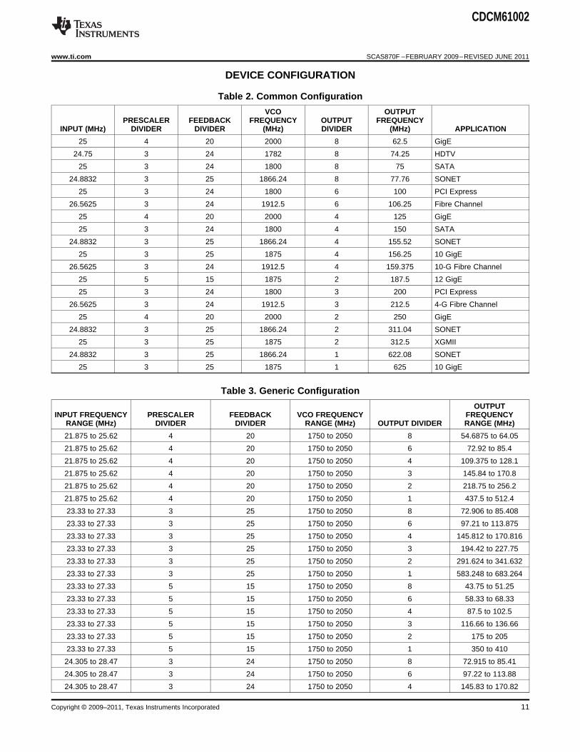
DEVICE CONFIGURATION
Table 2. Common Configuration
VCO OUTPUTPRESCALER FEEDBACK FREQUENCY OUTPUT FREQUENCY
INPUT (MHz) DIVIDER DIVIDER (MHz) DIVIDER (MHz) APPLICATION
25 4 20 2000 8 62.5 GigE
24.75 3 24 1782 8 74.25 HDTV
25 3 24 1800 8 75 SATA
24.8832 3 25 1866.24 8 77.76 SONET
25 3 24 1800 6 100 PCI Express
26.5625 3 24 1912.5 6 106.25 Fibre Channel
25 4 20 2000 4 125 GigE
25 3 24 1800 4 150 SATA
24.8832 3 25 1866.24 4 155.52 SONET
25 3 25 1875 4 156.25 10 GigE
26.5625 3 24 1912.5 4 159.375 10-G Fibre Channel
25 5 15 1875 2 187.5 12 GigE
25 3 24 1800 3 200 PCI Express
26.5625 3 24 1912.5 3 212.5 4-G Fibre Channel
25 4 20 2000 2 250 GigE
24.8832 3 25 1866.24 2 311.04 SONET
25 3 25 1875 2 312.5 XGMII
24.8832 3 25 1866.24 1 622.08 SONET
25 3 25 1875 1 625 10 GigE
Table 3. Generic Configuration
OUTPUTINPUT FREQUENCY PRESCALER FEEDBACK VCO FREQUENCY FREQUENCY
RANGE (MHz) DIVIDER DIVIDER RANGE (MHz) OUTPUT DIVIDER RANGE (MHz)
21.875 to 25.62 4 20 1750 to 2050 8 54.6875 to 64.05
21.875 to 25.62 4 20 1750 to 2050 6 72.92 to 85.4
21.875 to 25.62 4 20 1750 to 2050 4 109.375 to 128.1
21.875 to 25.62 4 20 1750 to 2050 3 145.84 to 170.8
21.875 to 25.62 4 20 1750 to 2050 2 218.75 to 256.2
21.875 to 25.62 4 20 1750 to 2050 1 437.5 to 512.4
23.33 to 27.33 3 25 1750 to 2050 8 72.906 to 85.408
23.33 to 27.33 3 25 1750 to 2050 6 97.21 to 113.875
23.33 to 27.33 3 25 1750 to 2050 4 145.812 to 170.816
23.33 to 27.33 3 25 1750 to 2050 3 194.42 to 227.75
23.33 to 27.33 3 25 1750 to 2050 2 291.624 to 341.632
23.33 to 27.33 3 25 1750 to 2050 1 583.248 to 683.264
23.33 to 27.33 5 15 1750 to 2050 8 43.75 to 51.25
23.33 to 27.33 5 15 1750 to 2050 6 58.33 to 68.33
23.33 to 27.33 5 15 1750 to 2050 4 87.5 to 102.5
23.33 to 27.33 5 15 1750 to 2050 3 116.66 to 136.66
23.33 to 27.33 5 15 1750 to 2050 2 175 to 205
23.33 to 27.33 5 15 1750 to 2050 1 350 to 410
24.305 to 28.47 3 24 1750 to 2050 8 72.915 to 85.41
24.305 to 28.47 3 24 1750 to 2050 6 97.22 to 113.88
24.305 to 28.47 3 24 1750 to 2050 4 145.83 to 170.82
Copyright © 2009–2011, Texas Instruments Incorporated 11
CDCM61002
SCAS870F –FEBRUARY 2009–REVISED JUNE 2011 www.ti.com
Table 3. Generic Configuration (continued)
OUTPUTINPUT FREQUENCY PRESCALER FEEDBACK VCO FREQUENCY FREQUENCY
RANGE (MHz) DIVIDER DIVIDER RANGE (MHz) OUTPUT DIVIDER RANGE (MHz)
24.305 to 28.47 3 24 1750 to 2050 3 194.44 to 227.76
24.305 to 28.47 3 24 1750 to 2050 2 291.66 to 341.64
24.305 to 28.47 3 24 1750 to 2050 1 583.32 to 683.28
Table 4. Programmable Prescaler and Feedback Divider Settings
CONTROL INPUTS PFD FREQUENCYPRESCALER FEEDBACKPR1 PR0 DIVIDER DIVIDER MINIMUM MAXIMUM
0 0 3 24 24.305 28.47
0 1 5 15 23.33 27.33
1 0 3 25 23.33 27.33
1 1 4 20 21.875 25.62
Table 5. Programmable Output Divider
CONTROL INPUTS
OD2 OD1 OD0 OUTPUT DIVIDER
0 0 0 1
0 0 1 2
0 1 0 3
0 1 1 4
1 0 0 Reserved
1 0 1 6
1 1 0 Reserved
1 1 1 8
Table 6. Programmable Output Type
CONTROL INPUTS
OS1 OS0 OUTPUT TYPE
0 0 LVCMOS, OSC_OUT Off
0 1 LVDS, OSC_OUT Off
1 0 LVPECL, OSC_OUT Off
1 1 LVPECL, OSC_OUT On
Table 7. Output Enable
CONTROL INPUT OPERATINGCE CONDITION OUTPUT
0 Power Down Hi-Z
1 Normal Active
Table 8. Reset
CONTROL INPUT OPERATINGRSTN CONDITION OUTPUT
0 Device Reset Hi-Z
0 → 1 PLL Recalibration Hi-Z
1 Normal Active
12 Copyright © 2009–2011, Texas Instruments Incorporated
145
140
135
130
125
120
Supply
CU
rrent (m
A)
0 200 400 600 800
Output Frequency (MHz)
Output-divide-by-8
Output-divide-by-6
Output-divide-by-4
Output-divide-by-3
Output-divide-by-2
Output-divide-by-1
130
125
120
115
110
105
Supply
CU
rrent (m
A)
0 200 400 600 800
Output Frequency (MHz)
Output-divide-by-8
Output-divide-by-6
Output-divide-by-4
Output-divide-by-3
Output-divide-by-2
Output-divide-by-1
CDCM61002
www.ti.com SCAS870F –FEBRUARY 2009–REVISED JUNE 2011
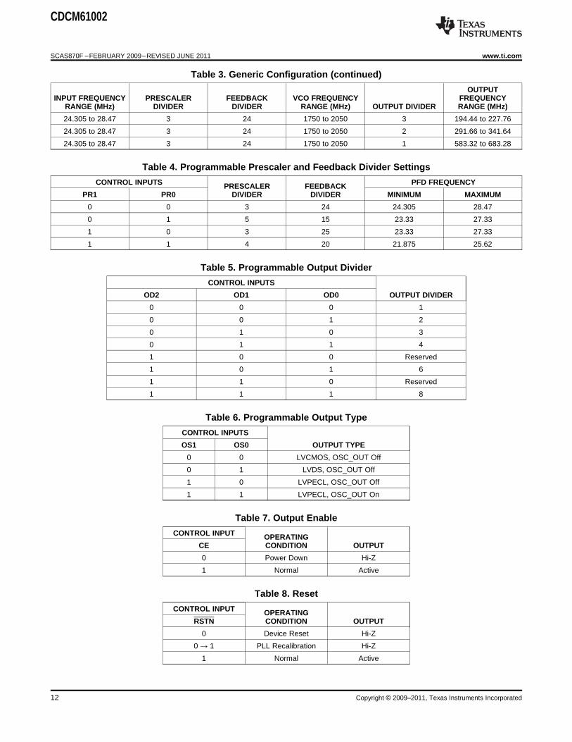
TYPICAL CHARACTERISTICSOver operating free-air temperature range (unless otherwise noted).
TYPICAL CURRENT CONSUMPTION FOR LVPECL OUTPUTvs OUTPUT FREQUENCY
Figure 3.
TYPICAL CURRENT CONSUMPTION FOR LVDS OUTPUTvs OUTPUT FREQUENCY
Figure 4.
Copyright © 2009–2011, Texas Instruments Incorporated 13
130
125
120
115
110
105
100
95
90
Supply
Curr
ent (m
A)
0 50 100 150 200 250 300
Output Frequency (MHz)
Output-divide-by-8
Output-divide-by-6
Output-divide-by-4
Output-divide-by-3
Output-divide-by-2
0.77
0.76
0.75
0.74
0.73
0.72
0.71
0.70
Diffe
rential O
utp
ut V
oltage, V
(V)
OD
0 100 200 300 400 500 600 700
Output Frequency (MHz)
CDCM61002
SCAS870F –FEBRUARY 2009–REVISED JUNE 2011 www.ti.com
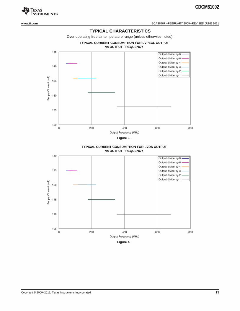
TYPICAL CHARACTERISTICS (continued)Over operating free-air temperature range (unless otherwise noted).
TYPICAL CURRENT CONSUMPTION FOR LVCMOS OUTPUTWITH 5-pF LOAD vs OUTPUT FREQUENCY
Figure 5.
TYPICAL LVPECL DIFFERENTIAL OUTPUT VOLTAGEvs OUTPUT FREQUENCY
Figure 6.
14 Copyright © 2009–2011, Texas Instruments Incorporated
0.42
0.40
0.38
0.36
0.34
0.32
0.30
Diffe
ren
tia
l O
utp
ut
Vo
lta
ge
, V
(V)
DO
0 100 200 300 400 500 600 700
Output Frequency (MHz)
3.30
3.25
3.20
3.15
3.10
3.05
3.00
Ou
tpu
t V
olta
ge
, V
(V)
OU
T
50 100 150 200 250
Output Frequency (MHz)
CDCM61002
www.ti.com SCAS870F –FEBRUARY 2009–REVISED JUNE 2011
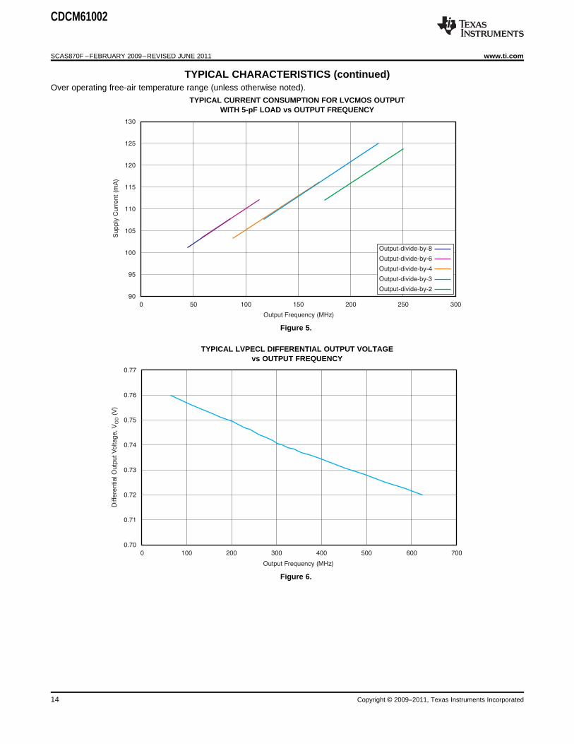
TYPICAL CHARACTERISTICS (continued)Over operating free-air temperature range (unless otherwise noted).
TYPICAL LVDS DIFFERENTIAL OUTPUT VOLTAGEvs OUTPUT FREQUENCY
Figure 7.
TYPICAL LVCMOS OUTPUT VOLTAGE WITH 5-pF LOADvs OUTPUT FREQUENCY
Figure 8.
Copyright © 2009–2011, Texas Instruments Incorporated 15
5 pF
LVCMOS
LVCMOSPhase Noise
Analyzer
LVPECL Oscilloscope
50 W50 W
VCC 2V-
LVPECL
150 W 50 W
Phase Noise
Analyzer
150 W
CDCM61002
SCAS870F –FEBRUARY 2009–REVISED JUNE 2011 www.ti.com
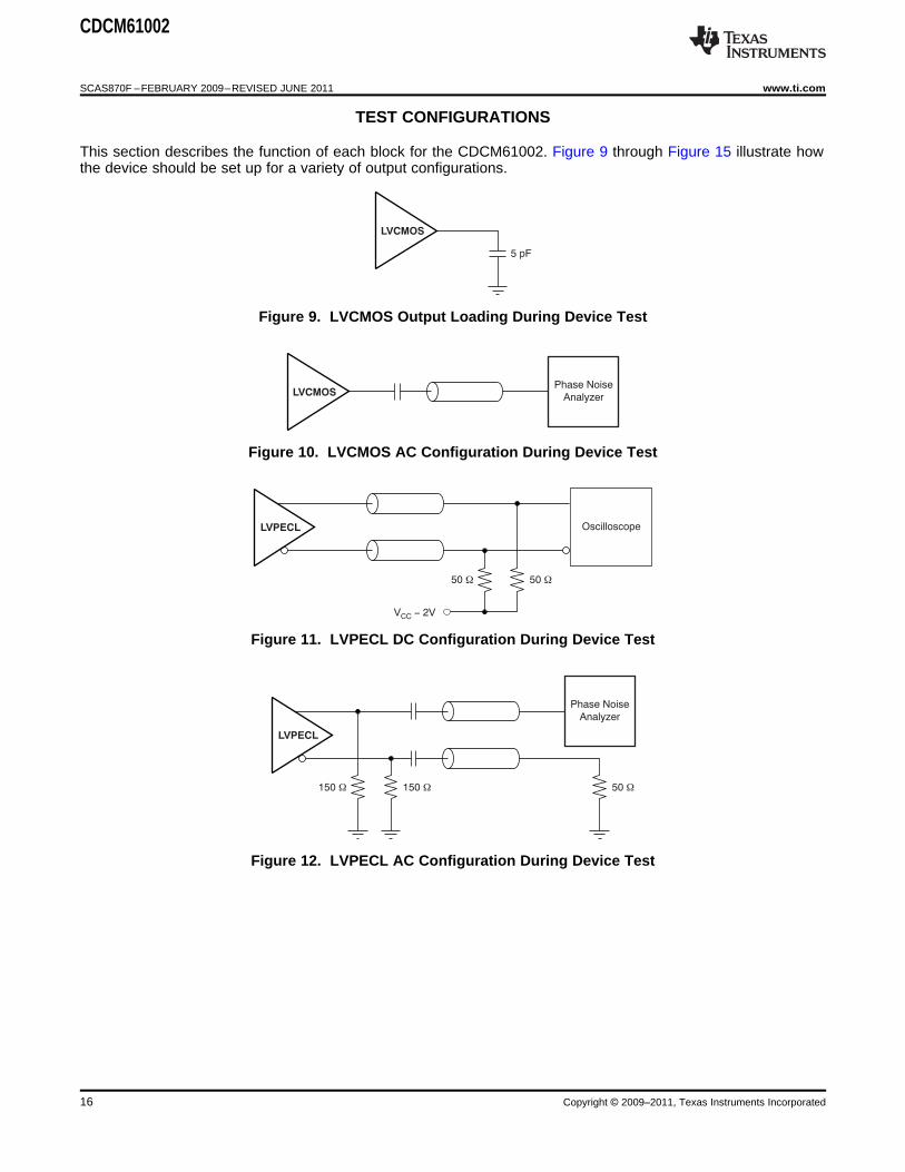
TEST CONFIGURATIONS
This section describes the function of each block for the CDCM61002. Figure 9 through Figure 15 illustrate howthe device should be set up for a variety of output configurations.
Figure 9. LVCMOS Output Loading During Device Test
Figure 10. LVCMOS AC Configuration During Device Test
Figure 11. LVPECL DC Configuration During Device Test
Figure 12. LVPECL AC Configuration During Device Test
16 Copyright © 2009–2011, Texas Instruments Incorporated
LVDS 100 W Oscilloscope
LVDS
Phase Noise
Analyzer
50 W
Yx
Yx VOL
VOH
VOD
0 V
80%
20%
tr tf
VOUTpp
CDCM61002
www.ti.com SCAS870F –FEBRUARY 2009–REVISED JUNE 2011
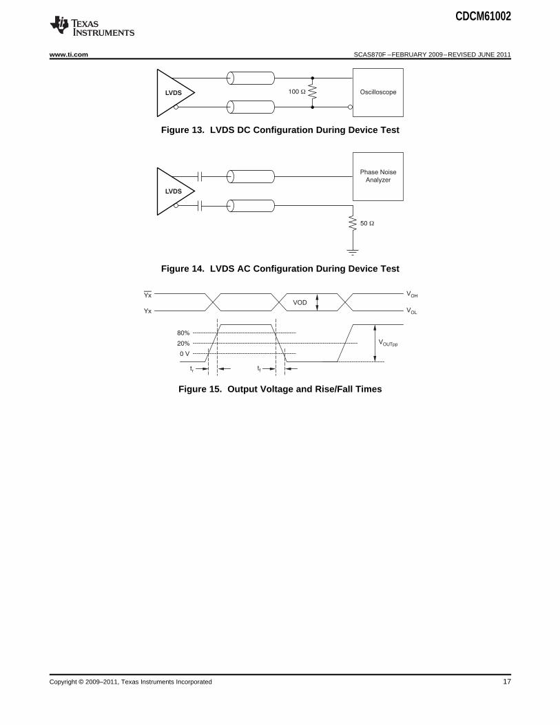
Figure 13. LVDS DC Configuration During Device Test
Figure 14. LVDS AC Configuration During Device Test
Figure 15. Output Voltage and Rise/Fall Times
Copyright © 2009–2011, Texas Instruments Incorporated 17
Df
f
CS
2(C + C )L,R O
=CS
2(C + C )L,A O
-
CDCM61002
SCAS870F –FEBRUARY 2009–REVISED JUNE 2011 www.ti.com
FUNCTIONAL DESCRIPTION
Phase-Locked Loop (PLL)
The CDCM61002 includes an on-chip PLL with an on-chip VCO. The PLL blocks consist of a crystal inputinterface, which can also accept an LVCMOS signal, a phase frequency detector (PFD), a charge pump, anon-chip loop filter, and prescaler and feedback dividers. Completing the CDCM61002 device are the outputdivider and universal output buffer.
The PLL is powered by on-chip, low-dropout (LDO) linear voltage regulators. The regulated supply network ispartitioned such that the sensitive analog supplies are powered from separate LDOs rather than the digitalsupplies which use a separate LDO regulator. These LDOs provide isolation for the PLL from any noise in theexternal power-supply rail. The REG_CAP1 and REG_CAP2 pins should each be connected to ground by 10-μFcapacitors to ensure stability.
Configuring the PLL
The CDCM61002 permits PLL configurations to accommodate the various input and output frequencies listed inTable 2 and Table 3. These configurations are accomplished by setting the prescaler divider, feedback dividerand output divider. The various dividers are managed by setting the device control pins as shown in Table 4 andTable 5.
Crystal Input Interface
Fundamental mode is the recommended oscillation mode of operation for the input crystal and parallelresonance is the recommended type of circuit for the crystal.
A crystal load capacitance refers to all capacitances in the oscillator feedback loop. It is equal to the amount ofcapacitance seen between the terminals of the crystal in the circuit. For parallel resonant mode circuits, thecorrect load capacitance is necessary to ensure the oscillation of the crystal within the expected parameters.
The CDCM61002 implements an input crystal oscillator circuitry, known as the Colpitts oscillator, and requiresone pad of the crystal to interface with the XIN pin; the other pad of the crystal is tied to ground. In this crystalinterface, it is important to account for all sources of capacitance when calculating the correct value for thediscrete capacitor component, CL, for a design.
The CDCM61002 has been characterized with 10-pF parallel resonant crystals. The input crystal oscillator stagein the CDCM61002 is designed to oscillate at the correct frequency for all parallel resonant crystals with low-pullcapability and rated with a load capacitance that is equal to the sum of the onchip load capacitance at the XINpin (10-pF), crystal stray capacitance, and board parasitic capacitance between the crystal and XIN pin.
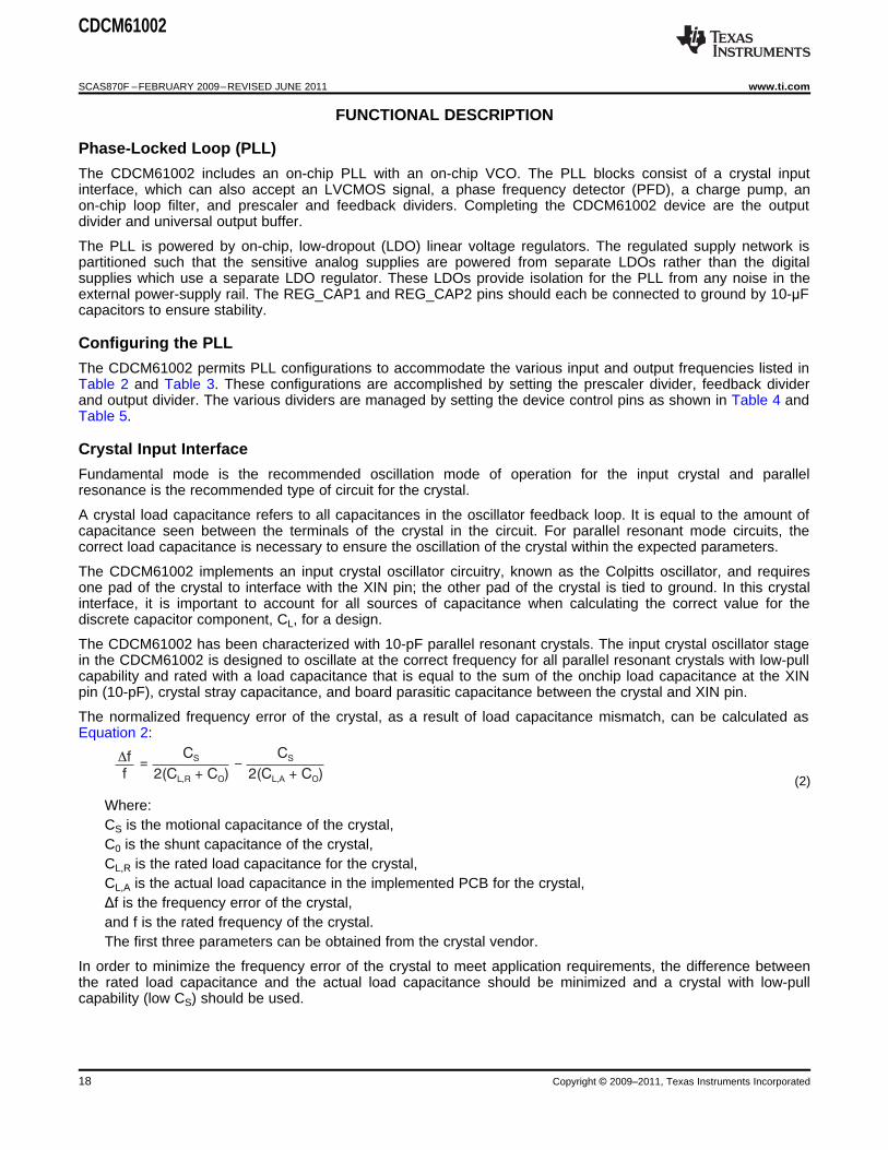
The normalized frequency error of the crystal, as a result of load capacitance mismatch, can be calculated asEquation 2:
(2)
Where:CS is the motional capacitance of the crystal,C0 is the shunt capacitance of the crystal,CL,R is the rated load capacitance for the crystal,CL,A is the actual load capacitance in the implemented PCB for the crystal,Δf is the frequency error of the crystal,and f is the rated frequency of the crystal.The first three parameters can be obtained from the crystal vendor.
In order to minimize the frequency error of the crystal to meet application requirements, the difference betweenthe rated load capacitance and the actual load capacitance should be minimized and a crystal with low-pullcapability (low CS) should be used.
18 Copyright © 2009–2011, Texas Instruments Incorporated
15 kW
20 kW473.5 pF
Charge Pump
OutputVCO Control
CDCM61002
www.ti.com SCAS870F –FEBRUARY 2009–REVISED JUNE 2011
For example, if an application requires less than ±50 ppm frequency error and a crystal with less than ±50 ppmfrequency tolerance is picked, the characteristics are as follows: C0 = 7 pF, CS = 10 fF, and CL,R = 12 pF. Inorder to meet the required frequency error, calculate CL,A using Equation 2 to be 17 pF. Subtracting CL,R fromCL,A, results in 5 pF; care must be taken during printed circuit board (PCB) layout with the crystal and theCDCM61002 to ensure that the sum of the crystal stray capacitance and board parisitic capacitance is less thanthe calculated 5 pF.
Good layout practices are fundamental to the correct operation and reliability of the oscillator. It is critical tolocate the crystal components very close to the XIN pin to minimize routing distances. Long traces in theoscillator circuit are a very common source of problems. Do not route other signals across the oscillator circuit.Also, make sure power and high-frequency traces are routed as far away as possible to avoid crosstalk andnoise coupling. Avoid the use of vias; if the routing becomes very complex, it is much better to use 0-Ω resistorsas bridges to go over other signals. Vias in the oscillator circuit should only be used for connections to theground plane. Do not share ground connections; instead, make a separate connection to ground for eachcomponent that requires grounding. If possible, place multiple vias in parallel for each connection to the groundplane. Especially in the Colpitts oscillator configuration, the oscillator is very sensitive to capacitance in parallelwith the crystal. Therefore, the layout must be designed to minimize stray capacitance across the crystal to lessthan 5 pF total under all circumstances to ensure proper crystal oscillation. Be sure to take into account bothPCB and crystal stray capacitance.
Table 9 lists several recommended crystals and the respective manufacturer of each.
Table 9. Recommended Crystal Manufacturers
MANUFACTURER PART NUMBER
Vectron VXC1-1133
Fox 218-3
Saronix FP2650002
Phase Frequency Detector (PFD)
The PFD takes inputs from the input interface and the feedback divider and produces an output that depends onthe phase and frequency differences between the two inputs. The allowable range of frequencies at the PFDinputs is 21.875 MHz to 28.47 MHz.
Charge Pump (CP)
The charge pump is controlled by the PFD, which dictates either to pump up or down in order to charge ordischarge the integrating section of the on-chip loop filter. The integrated and filtered charge pump current is thenconverted to a voltage that drives the control voltage node of the internal VCO through the on-chip loop filter. Thecharge pump current is preset to 224 μA and cannot be changed.
On-Chip PLL Loop Filter
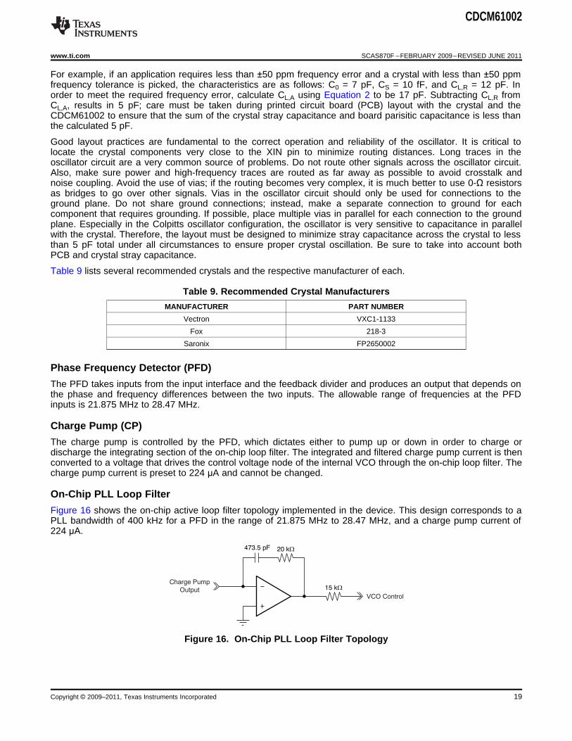
Figure 16 shows the on-chip active loop filter topology implemented in the device. This design corresponds to aPLL bandwidth of 400 kHz for a PFD in the range of 21.875 MHz to 28.47 MHz, and a charge pump current of224 μA.
Figure 16. On-Chip PLL Loop Filter Topology
Copyright © 2009–2011, Texas Instruments Incorporated 19
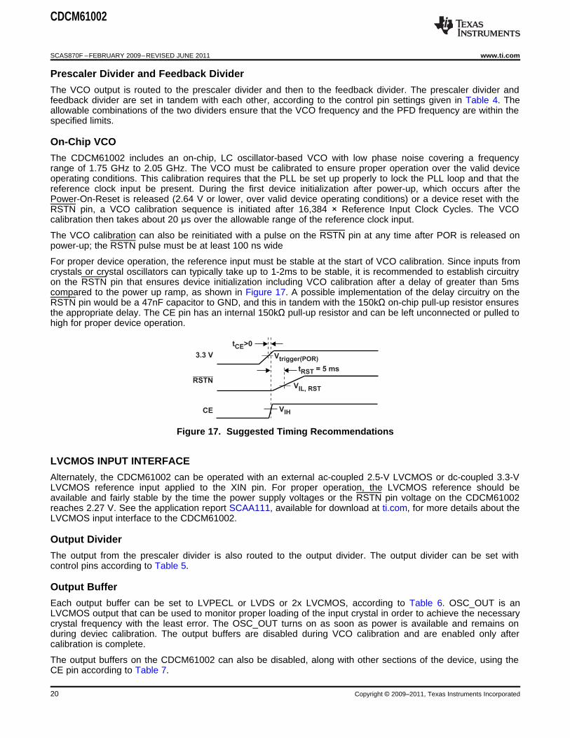
3.3 V
RSTN
CE
t >0CE
Vtrigger(POR)
t = 5 msRST
VIH
VIL, RST
CDCM61002
SCAS870F –FEBRUARY 2009–REVISED JUNE 2011 www.ti.com
Prescaler Divider and Feedback Divider
The VCO output is routed to the prescaler divider and then to the feedback divider. The prescaler divider andfeedback divider are set in tandem with each other, according to the control pin settings given in Table 4. Theallowable combinations of the two dividers ensure that the VCO frequency and the PFD frequency are within thespecified limits.
On-Chip VCO
The CDCM61002 includes an on-chip, LC oscillator-based VCO with low phase noise covering a frequencyrange of 1.75 GHz to 2.05 GHz. The VCO must be calibrated to ensure proper operation over the valid deviceoperating conditions. This calibration requires that the PLL be set up properly to lock the PLL loop and that thereference clock input be present. During the first device initialization after power-up, which occurs after thePower-On-Reset is released (2.64 V or lower, over valid device operating conditions) or a device reset with theRSTN pin, a VCO calibration sequence is initiated after 16,384 × Reference Input Clock Cycles. The VCOcalibration then takes about 20 µs over the allowable range of the reference clock input.
The VCO calibration can also be reinitiated with a pulse on the RSTN pin at any time after POR is released onpower-up; the RSTN pulse must be at least 100 ns wide
For proper device operation, the reference input must be stable at the start of VCO calibration. Since inputs fromcrystals or crystal oscillators can typically take up to 1-2ms to be stable, it is recommended to establish circuitryon the RSTN pin that ensures device initialization including VCO calibration after a delay of greater than 5mscompared to the power up ramp, as shown in Figure 17. A possible implementation of the delay circuitry on theRSTN pin would be a 47nF capacitor to GND, and this in tandem with the 150kΩ on-chip pull-up resistor ensuresthe appropriate delay. The CE pin has an internal 150kΩ pull-up resistor and can be left unconnected or pulled tohigh for proper device operation.
Figure 17. Suggested Timing Recommendations
LVCMOS INPUT INTERFACE
Alternately, the CDCM61002 can be operated with an external ac-coupled 2.5-V LVCMOS or dc-coupled 3.3-VLVCMOS reference input applied to the XIN pin. For proper operation, the LVCMOS reference should beavailable and fairly stable by the time the power supply voltages or the RSTN pin voltage on the CDCM61002reaches 2.27 V. See the application report SCAA111, available for download at ti.com, for more details about theLVCMOS input interface to the CDCM61002.
Output Divider
The output from the prescaler divider is also routed to the output divider. The output divider can be set withcontrol pins according to Table 5.
Output Buffer
Each output buffer can be set to LVPECL or LVDS or 2x LVCMOS, according to Table 6. OSC_OUT is anLVCMOS output that can be used to monitor proper loading of the input crystal in order to achieve the necessarycrystal frequency with the least error. The OSC_OUT turns on as soon as power is available and remains onduring deviec calibration. The output buffers are disabled during VCO calibration and are enabled only aftercalibration is complete.
The output buffers on the CDCM61002 can also be disabled, along with other sections of the device, using theCE pin according to Table 7.
20 Copyright © 2009–2011, Texas Instruments Incorporated
t =REF
1
fREF
Po
we
r S
up
ply
(V
)
Time (s)
2.27 V
2.64 V
tpul
tpuh
trsu
tdelay
tVCO_CAL
tPLL_LOCK
Power up
Reference
Startup Delay VCO Calibration PLL Lock
CDCM61002
www.ti.com SCAS870F –FEBRUARY 2009–REVISED JUNE 2011
APPLICATION INFORMATION
Start-up Time Estimation
The CDCM61002 startup time can be estimated based on the parameters defined in Table 10 and graphicallyshown in Figure 18.
Table 10. Start-up Time Dependencies
FORMULA/METHOD OFPARAMETER DEFINITION DESCRIPTION DETERMINATION
The reciprocal of the applied referencetREF Reference clock period frequency in seconds.
Power-supply rise time to low limit of Power Time required for powertpul Power-up time (low limit) On Reset (POR) trip point supply to ramp to 2.27 V
Power supply rise time to high limit of POR Time required for powertpuh Power-up time (high limit) trip point supply to ramp to 2.64 V
After POR releases, the Colpits oscillator isenabled. This start-up time is required for the 500 μs best-case and 800 μstrsu Reference start-up time oscillator to generate the requisite signal worst-caselevels for the delay block to be clocked bythe reference input.
Internal delay time generated from thetdelay Delay time reference clock. This delay provides time for tdelay= 16384 × tref
the reference oscillator to stabilize.
VCO Calibration Time generated from thereference clock. This process selects thetVCO_CAL VCO calibration time tVCO_CAL= 550 × trefoperating point for the VCO based on thePLL settings.
Based on the 400-kHz loopTime required for PLL to lock within ±10 ppmtPLL_LOCK PLL lock time bandwidth, the PLL settles inof fREF 5τ or 12.5 μs.
Figure 18. Start-up Time Dependencies
Copyright © 2009–2011, Texas Instruments Incorporated 21
CDCM61002
SCAS870F –FEBRUARY 2009–REVISED JUNE 2011 www.ti.com
The CDCM61002 start-up time limits, tMAX and tMIN, can be calculated as follows:
tMAX = tpuh + trsu + tdelay + tVCO_CAL + tPLL_LOCK
tMIN = tpul + trsu + tdelay + tVCO_CAL + tPLL_LOCK
Power Considerations
As a result of the different possible configurations of the CDCM61002, Table 11 is intended to provide enoughinformation on the estimated current consumption of the device. Unless otherwise noted, VCC = 3.3 V and TA =+25°C.
Table 11. Estimated Block Power Consumption
EXTERNALRESISTOR
POWERCURRENT CONSUMPTION IN-DEVICE POWER DISSIPATION DISSIPATION
BLOCK CONDITION (mA) (mW) (mW)
Entire device, Output off, no termination 65 214.5core current resistors
LVPECL output, active mode 28 42.4 50
LVCMOS output pair, static 4.5 14.85
LVCMOS output pair,Output buffertransient, 'CL' load, 'f' MHz V × fOUT × (CL + 20 × 10–12) × 103 V2 × fOUT × (CL + 20 × 10–12) × 103
output frequency
LVDS output, active mode 20 66
Divide enabled, divide = 1 5 16.5
Divide enabled, divide = 2 10 33Divide circuitry
Divide enabled, divide = 3, 4 15 49.5
Divide enabled, divide = 6, 8 20 66
From Table 11, the current consumption can be calculated for any configuration. For example, the current for theentire device with one LVPECL output in active mode can be calculated by adding up the following blocks: corecurrent, LVPECL output buffer current, and the divide circuitry current. The overall in-device power consumptioncan also be calculated by summing the in-device power dissipated in each of these blocks.
As an example scenario, let us consider the use case of a crystal input frequency of 25 MHz and device outputfrequency of 312.5 MHz in LVPECL mode. For this case, the typical overall power dissipation can be calculatedas:
3.3 V × (65 + 2 × 28 + 10) mA = 432.3 mW
Because the LVPECL output has external resistors and the power dissipated by these resistors is 50 mW, thetypical overall in-device power dissipation is:
432.3 mW – 2 × 50 mW = 332.3 mW
When the LVPECL output is active, the average voltage is approximately 1.9 V on each output as calculatedfrom the LVPECL VOH and VOL specifications. Therefore, the power dissipated in each emitter resistor isapproximately (1.9 V)2/150Ω = 25 mW.
When the LVCMOS output is active and drives a load capacitance, CL, the overall LVCMOS output currentconsumption is the sum of a static pre-driver current and a dynamic switching current (which is a function of theoutput frequency and the load capacitance).
Let us consider another use case of a crystal input frequency of 26.5625 MHz and device output frequency of212.5 MHz in LVCMOS mode and driving a 5-pF load capacitance. For this case, the typical overall powerdissipation can be calculated as:
3.3 V × (65 + 15 + 2 × 21.4) mA = 405.24 mW
22 Copyright © 2009–2011, Texas Instruments Incorporated
CDCM61002
www.ti.com SCAS870F –FEBRUARY 2009–REVISED JUNE 2011
Thermal Management
Power consumption of the CDCM61002 can be high enough to require attention to thermal management. Forreliability and performance reasons, the die temperature should be limited to a maximum of +125°C. That is, asan estimate, TA (ambient temperature) plus device power consumption times θJA should not exceed +125°C.
The device package has an exposed pad that provides the primary heat removal path as well as an electricalgrounding to the printed circuit board (PCB). To maximize the removal of heat from the package, a thermal landpattern including multiple vias to a ground plane must be incorporated on the PCB within the footprint of thepackage. The exposed pad must be soldered down to ensure adequate heat conduction out of the package.Check the mechanical data at the end of the data sheet for land and via pattern examples.
Power-Supply Filtering
PLL-based frequency synthesizers are very sensitive to noise on the power supply, which can dramaticallyincrease the jitter of the PLL. This characteristic is especially true for analog-based PLLs. Thus, it is essential toreduce noise from the system power supply, especially when jitter/phase noise is very critical to applications. APLL would have attenuated jitter as a result of power-supply noise at frequencies beyond the PLL bandwidthbecause of attenuation by the loop response.
Filter capacitors are used to eliminate the low-frequency noise from the power supply, where the bypasscapacitors provide the very low impedance path for high-frequency noise and guard the power-supply systemagainst the induced fluctuations. These bypass capacitors also provide instantaneous current surges as requiredby the device and should have low equivalent series resistance (ESR). To properly use these bypass capacitors,they must be placed very close to the power-supply pins and laid out with short loops to minimize inductance. Itis recommended to add as many high-frequency (for example, 0.1-μF) bypass capacitors as there are supplypins in the package.
The CDCM61002 power-supply requirements can be grouped into two sets: the analog supply line and theoutput/input supply line. The analog supply line consists of the following power-supply pins on the CDCM61002:VCC_PLL1, VCC_PLL2, and VCC_VCO. These pins can be shorted together. The output/input supply lineconsists of the VCC_OUT and the VCC_IN power-supply pins on the CDCM61002. These pins can be shortedtogether. Inserting a ferrite bead between the analog supply line and the output/input supply line isolates thehigh-frequency switching noises generated by the device input and outputs, preventing them from leaking intothe sensitive analog supply line. Choosing an appropriate ferrite bead with very low dc resistance is importantbecause it is imperative to provide adequate isolation between the sensitive analog supply line and the otherboard supply lines, and to maintain a voltage at the analog power-supply pins of the CDCM61002 that is greaterthan the minimum voltage required for proper operation.
Copyright © 2009–2011, Texas Instruments Incorporated 23
Analog
Supply
C
0.1 mF (x3)
C
10 FmC
10 Fm
C
0.1 F (x3)m
Ferrite Bead
Board/
Supply
Output/Input
CDCM61002 LVPECL
82 W82 W
130 W 130 W
VCC_OUT VCC_OUT
CDCM61002 LVPECL
50 W50 W150 W150 W
VBB
CDCM61002
SCAS870F –FEBRUARY 2009–REVISED JUNE 2011 www.ti.com
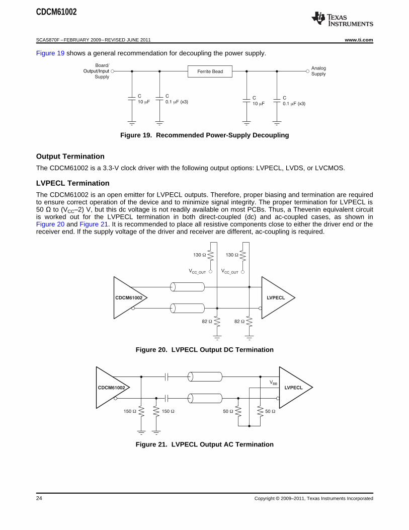
Figure 19 shows a general recommendation for decoupling the power supply.
Figure 19. Recommended Power-Supply Decoupling
Output Termination
The CDCM61002 is a 3.3-V clock driver with the following output options: LVPECL, LVDS, or LVCMOS.
LVPECL Termination
The CDCM61002 is an open emitter for LVPECL outputs. Therefore, proper biasing and termination are requiredto ensure correct operation of the device and to minimize signal integrity. The proper termination for LVPECL is50 Ω to (VCC–2) V, but this dc voltage is not readily available on most PCBs. Thus, a Thevenin equivalent circuitis worked out for the LVPECL termination in both direct-coupled (dc) and ac-coupled cases, as shown inFigure 20 and Figure 21. It is recommended to place all resistive components close to either the driver end or thereceiver end. If the supply voltage of the driver and receiver are different, ac-coupling is required.
Figure 20. LVPECL Output DC Termination
Figure 21. LVPECL Output AC Termination
24 Copyright © 2009–2011, Texas Instruments Incorporated
100 WCDCM61002 LVDS
100 WCDCM61002 LVDS
CDCM61002 LVCMOS
R = 22 WS
CDCM61002
www.ti.com SCAS870F –FEBRUARY 2009–REVISED JUNE 2011
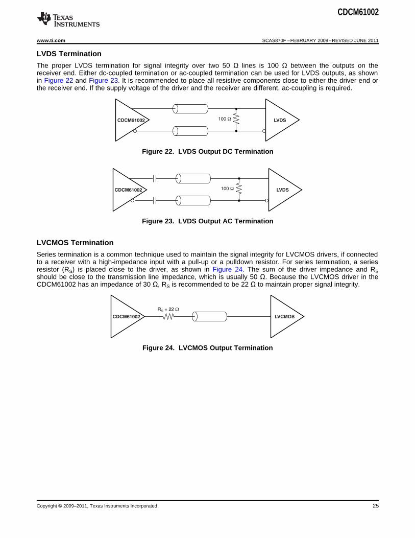
LVDS Termination
The proper LVDS termination for signal integrity over two 50 Ω lines is 100 Ω between the outputs on thereceiver end. Either dc-coupled termination or ac-coupled termination can be used for LVDS outputs, as shownin Figure 22 and Figure 23. It is recommended to place all resistive components close to either the driver end orthe receiver end. If the supply voltage of the driver and the receiver are different, ac-coupling is required.
Figure 22. LVDS Output DC Termination
Figure 23. LVDS Output AC Termination
LVCMOS Termination
Series termination is a common technique used to maintain the signal integrity for LVCMOS drivers, if connectedto a receiver with a high-impedance input with a pull-up or a pulldown resistor. For series termination, a seriesresistor (RS) is placed close to the driver, as shown in Figure 24. The sum of the driver impedance and RSshould be close to the transmission line impedance, which is usually 50 Ω. Because the LVCMOS driver in theCDCM61002 has an impedance of 30 Ω, RS is recommended to be 22 Ω to maintain proper signal integrity.
Figure 24. LVCMOS Output Termination
Copyright © 2009–2011, Texas Instruments Incorporated 25
HCSL
56 W56 W
471 W 471 W
CDCM61002
150 W150 W
0 W
0 W
VCC_OUT VCC_OUT
CDCM61002
SCAS870F –FEBRUARY 2009–REVISED JUNE 2011 www.ti.com
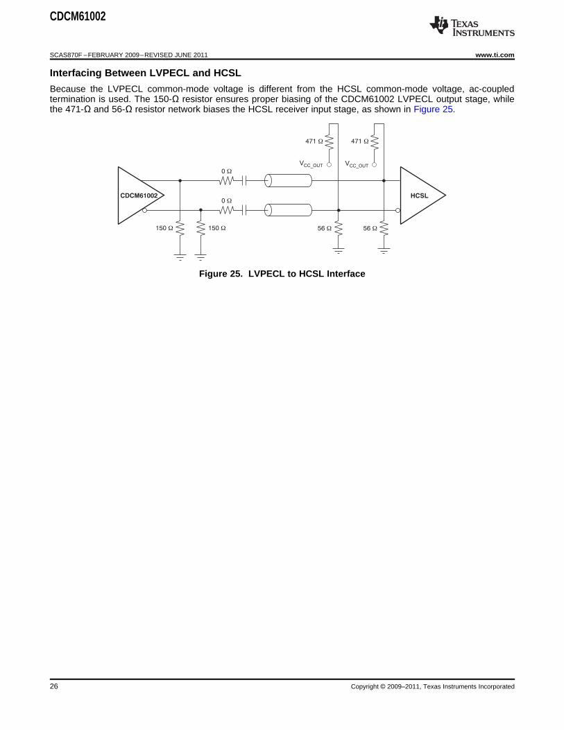
Interfacing Between LVPECL and HCSL
Because the LVPECL common-mode voltage is different from the HCSL common-mode voltage, ac-coupledtermination is used. The 150-Ω resistor ensures proper biasing of the CDCM61002 LVPECL output stage, whilethe 471-Ω and 56-Ω resistor network biases the HCSL receiver input stage, as shown in Figure 25.
Figure 25. LVPECL to HCSL Interface
26 Copyright © 2009–2011, Texas Instruments Incorporated
CDCM61002
www.ti.com SCAS870F –FEBRUARY 2009–REVISED JUNE 2011
REVISION HISTORY
NOTE: Page numbers for previous revisions may differ from page numbers in the current version.
Changes from Revision B (July, 2009) to Revision C Page
• Deleted references to Single-Ended and LVCMOS input throughout document ................................................................. 1
• Deleted fIN, ΔV/ΔT, and DutyREF parameters from Electrical Characteristics ..................................................................... 4
• Added LVCMOS Input Interface section ............................................................................................................................. 20
Changes from Revision C (February 2010) to Revision D Page
• Added reference to LVCMOS reference in first Features bullet ........................................................................................... 1
• Added reference to LVCMOS input in first paragraph of Description ................................................................................... 1
• Updated Figure 1 .................................................................................................................................................................. 2
• Changed name of Control Pin LVCMOS Input Characteristics section in Electrical Characteristics table .......................... 4
• Added reference to LVCMOS input in XIN parameter of Pin Functions table ...................................................................... 8
• Changed description of Crystal Input Interface section ...................................................................................................... 18
• Changed description of LVCMOS Input Interface section .................................................................................................. 20
Changes from Revision D (July 2010) to Revision E Page
• Changed Note 1 of the Pin Functions table From: Pull-up and Pull-down refer to...To:Pull-up refers to ............................. 8
• Deleted RPULLDOWN from Table 1 ........................................................................................................................................... 8
• Changed values in row 24.75 of Table 2 ............................................................................................................................ 11
• Changed the text of Configuring the PLL, deleted the last sentence ................................................................................. 18
• Changed the On-Chip VCO section .................................................................................................................................... 20
• Changed the Output Buffer section .................................................................................................................................... 20
• Changed the power dissipation equation From: 3.3 V × (65 + 2 × 28 + 10) mA = 429 mW To: 3.3 V × (65 + 2 × 28 +10) mA = 432.3 mW ............................................................................................................................................................ 22
• Changed the power dissipation equation From: 439 mW – 2 × 50 mW = 339 mW To: 432.3 mW – 2 × 50 mW =332.3 mW ............................................................................................................................................................................ 22
• Deleted figure "Recommended PCB Layout for CDCM61001" from the Thermal Management section. Added text"See the mechanical data at the end of the data sheet.." .................................................................................................. 23
Changes from Revision E (March 2011) to Revision F Page
• Changed the On-Chip VCO section .................................................................................................................................... 20
• Changed Figure 17 ............................................................................................................................................................. 20
• Moved the LVCMOS INPUT INTERFACE section prior to the Output Divider section ...................................................... 20
Copyright © 2009–2011, Texas Instruments Incorporated 27
PACKAGE OPTION ADDENDUM
www.ti.com 9-Aug-2017
Addendum-Page 1
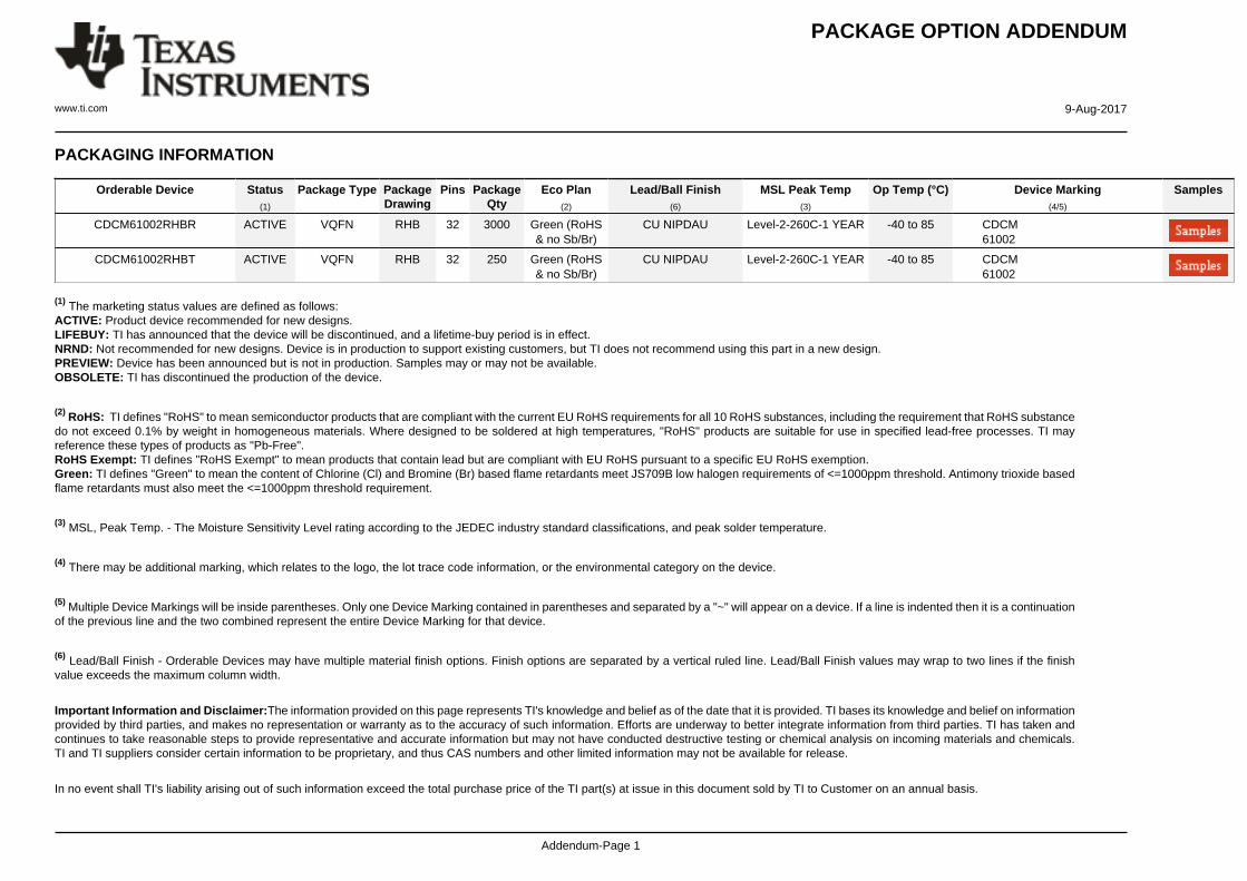
PACKAGING INFORMATION
Orderable Device Status(1)
Package Type PackageDrawing
Pins PackageQty
Eco Plan(2)
Lead/Ball Finish(6)
MSL Peak Temp(3)
Op Temp (°C) Device Marking(4/5)
Samples
CDCM61002RHBR ACTIVE VQFN RHB 32 3000 Green (RoHS& no Sb/Br)
CU NIPDAU Level-2-260C-1 YEAR -40 to 85 CDCM61002
CDCM61002RHBT ACTIVE VQFN RHB 32 250 Green (RoHS& no Sb/Br)
CU NIPDAU Level-2-260C-1 YEAR -40 to 85 CDCM61002
(1) The marketing status values are defined as follows:ACTIVE: Product device recommended for new designs.LIFEBUY: TI has announced that the device will be discontinued, and a lifetime-buy period is in effect.NRND: Not recommended for new designs. Device is in production to support existing customers, but TI does not recommend using this part in a new design.PREVIEW: Device has been announced but is not in production. Samples may or may not be available.OBSOLETE: TI has discontinued the production of the device.
(2) RoHS: TI defines "RoHS" to mean semiconductor products that are compliant with the current EU RoHS requirements for all 10 RoHS substances, including the requirement that RoHS substancedo not exceed 0.1% by weight in homogeneous materials. Where designed to be soldered at high temperatures, "RoHS" products are suitable for use in specified lead-free processes. TI mayreference these types of products as "Pb-Free".RoHS Exempt: TI defines "RoHS Exempt" to mean products that contain lead but are compliant with EU RoHS pursuant to a specific EU RoHS exemption.Green: TI defines "Green" to mean the content of Chlorine (Cl) and Bromine (Br) based flame retardants meet JS709B low halogen requirements of <=1000ppm threshold. Antimony trioxide basedflame retardants must also meet the <=1000ppm threshold requirement.
(3) MSL, Peak Temp. - The Moisture Sensitivity Level rating according to the JEDEC industry standard classifications, and peak solder temperature.
(4) There may be additional marking, which relates to the logo, the lot trace code information, or the environmental category on the device.
(5) Multiple Device Markings will be inside parentheses. Only one Device Marking contained in parentheses and separated by a "~" will appear on a device. If a line is indented then it is a continuationof the previous line and the two combined represent the entire Device Marking for that device.
(6) Lead/Ball Finish - Orderable Devices may have multiple material finish options. Finish options are separated by a vertical ruled line. Lead/Ball Finish values may wrap to two lines if the finishvalue exceeds the maximum column width.
Important Information and Disclaimer:The information provided on this page represents TI's knowledge and belief as of the date that it is provided. TI bases its knowledge and belief on informationprovided by third parties, and makes no representation or warranty as to the accuracy of such information. Efforts are underway to better integrate information from third parties. TI has taken andcontinues to take reasonable steps to provide representative and accurate information but may not have conducted destructive testing or chemical analysis on incoming materials and chemicals.TI and TI suppliers consider certain information to be proprietary, and thus CAS numbers and other limited information may not be available for release.
In no event shall TI's liability arising out of such information exceed the total purchase price of the TI part(s) at issue in this document sold by TI to Customer on an annual basis.
PACKAGE OPTION ADDENDUM
www.ti.com 9-Aug-2017
Addendum-Page 2
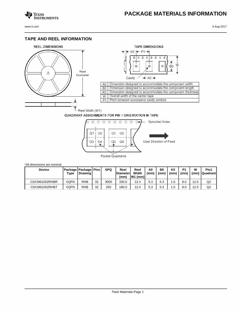
TAPE AND REEL INFORMATION
*All dimensions are nominal
Device PackageType
PackageDrawing
Pins SPQ ReelDiameter
(mm)
ReelWidth
W1 (mm)
A0(mm)
B0(mm)
K0(mm)
P1(mm)
W(mm)
Pin1Quadrant
CDCM61002RHBR VQFN RHB 32 3000 330.0 12.4 5.3 5.3 1.5 8.0 12.0 Q2
CDCM61002RHBT VQFN RHB 32 250 180.0 12.4 5.3 5.3 1.5 8.0 12.0 Q2
PACKAGE MATERIALS INFORMATION
www.ti.com 3-Aug-2017
Pack Materials-Page 1
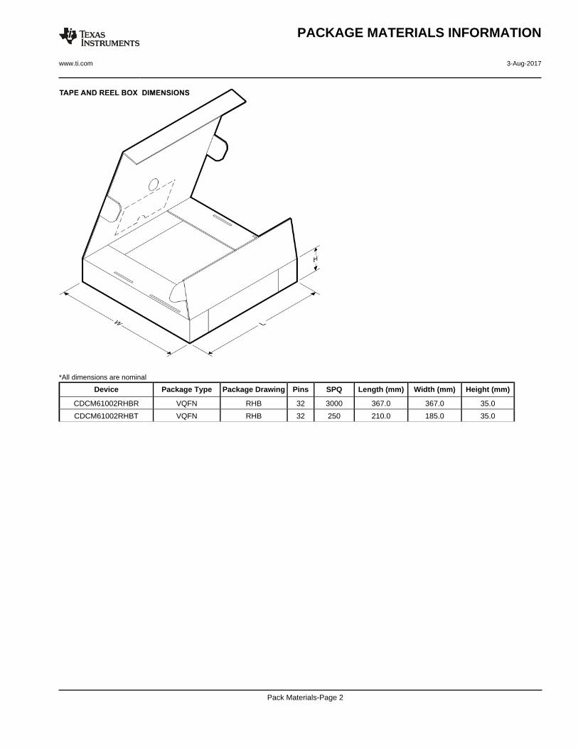
*All dimensions are nominal
Device Package Type Package Drawing Pins SPQ Length (mm) Width (mm) Height (mm)
CDCM61002RHBR VQFN RHB 32 3000 367.0 367.0 35.0
CDCM61002RHBT VQFN RHB 32 250 210.0 185.0 35.0
PACKAGE MATERIALS INFORMATION
www.ti.com 3-Aug-2017
Pack Materials-Page 2
IMPORTANT NOTICE
Texas Instruments Incorporated (TI) reserves the right to make corrections, enhancements, improvements and other changes to itssemiconductor products and services per JESD46, latest issue, and to discontinue any product or service per JESD48, latest issue. Buyersshould obtain the latest relevant information before placing orders and should verify that such information is current and complete.TI’s published terms of sale for semiconductor products (http://www.ti.com/sc/docs/stdterms.htm) apply to the sale of packaged integratedcircuit products that TI has qualified and released to market. Additional terms may apply to the use or sale of other types of TI products andservices.Reproduction of significant portions of TI information in TI data sheets is permissible only if reproduction is without alteration and isaccompanied by all associated warranties, conditions, limitations, and notices. TI is not responsible or liable for such reproduceddocumentation. Information of third parties may be subject to additional restrictions. Resale of TI products or services with statementsdifferent from or beyond the parameters stated by TI for that product or service voids all express and any implied warranties for theassociated TI product or service and is an unfair and deceptive business practice. TI is not responsible or liable for any such statements.Buyers and others who are developing systems that incorporate TI products (collectively, “Designers”) understand and agree that Designersremain responsible for using their independent analysis, evaluation and judgment in designing their applications and that Designers havefull and exclusive responsibility to assure the safety of Designers' applications and compliance of their applications (and of all TI productsused in or for Designers’ applications) with all applicable regulations, laws and other applicable requirements. Designer represents that, withrespect to their applications, Designer has all the necessary expertise to create and implement safeguards that (1) anticipate dangerousconsequences of failures, (2) monitor failures and their consequences, and (3) lessen the likelihood of failures that might cause harm andtake appropriate actions. Designer agrees that prior to using or distributing any applications that include TI products, Designer willthoroughly test such applications and the functionality of such TI products as used in such applications.TI’s provision of technical, application or other design advice, quality characterization, reliability data or other services or information,including, but not limited to, reference designs and materials relating to evaluation modules, (collectively, “TI Resources”) are intended toassist designers who are developing applications that incorporate TI products; by downloading, accessing or using TI Resources in anyway, Designer (individually or, if Designer is acting on behalf of a company, Designer’s company) agrees to use any particular TI Resourcesolely for this purpose and subject to the terms of this Notice.TI’s provision of TI Resources does not expand or otherwise alter TI’s applicable published warranties or warranty disclaimers for TIproducts, and no additional obligations or liabilities arise from TI providing such TI Resources. TI reserves the right to make corrections,enhancements, improvements and other changes to its TI Resources. TI has not conducted any testing other than that specificallydescribed in the published documentation for a particular TI Resource.Designer is authorized to use, copy and modify any individual TI Resource only in connection with the development of applications thatinclude the TI product(s) identified in such TI Resource. NO OTHER LICENSE, EXPRESS OR IMPLIED, BY ESTOPPEL OR OTHERWISETO ANY OTHER TI INTELLECTUAL PROPERTY RIGHT, AND NO LICENSE TO ANY TECHNOLOGY OR INTELLECTUAL PROPERTYRIGHT OF TI OR ANY THIRD PARTY IS GRANTED HEREIN, including but not limited to any patent right, copyright, mask work right, orother intellectual property right relating to any combination, machine, or process in which TI products or services are used. Informationregarding or referencing third-party products or services does not constitute a license to use such products or services, or a warranty orendorsement thereof. Use of TI Resources may require a license from a third party under the patents or other intellectual property of thethird party, or a license from TI under the patents or other intellectual property of TI.TI RESOURCES ARE PROVIDED “AS IS” AND WITH ALL FAULTS. TI DISCLAIMS ALL OTHER WARRANTIES ORREPRESENTATIONS, EXPRESS OR IMPLIED, REGARDING RESOURCES OR USE THEREOF, INCLUDING BUT NOT LIMITED TOACCURACY OR COMPLETENESS, TITLE, ANY EPIDEMIC FAILURE WARRANTY AND ANY IMPLIED WARRANTIES OFMERCHANTABILITY, FITNESS FOR A PARTICULAR PURPOSE, AND NON-INFRINGEMENT OF ANY THIRD PARTY INTELLECTUALPROPERTY RIGHTS. TI SHALL NOT BE LIABLE FOR AND SHALL NOT DEFEND OR INDEMNIFY DESIGNER AGAINST ANY CLAIM,INCLUDING BUT NOT LIMITED TO ANY INFRINGEMENT CLAIM THAT RELATES TO OR IS BASED ON ANY COMBINATION OFPRODUCTS EVEN IF DESCRIBED IN TI RESOURCES OR OTHERWISE. IN NO EVENT SHALL TI BE LIABLE FOR ANY ACTUAL,DIRECT, SPECIAL, COLLATERAL, INDIRECT, PUNITIVE, INCIDENTAL, CONSEQUENTIAL OR EXEMPLARY DAMAGES INCONNECTION WITH OR ARISING OUT OF TI RESOURCES OR USE THEREOF, AND REGARDLESS OF WHETHER TI HAS BEENADVISED OF THE POSSIBILITY OF SUCH DAMAGES.Unless TI has explicitly designated an individual product as meeting the requirements of a particular industry standard (e.g., ISO/TS 16949and ISO 26262), TI is not responsible for any failure to meet such industry standard requirements.Where TI specifically promotes products as facilitating functional safety or as compliant with industry functional safety standards, suchproducts are intended to help enable customers to design and create their own applications that meet applicable functional safety standardsand requirements. Using products in an application does not by itself establish any safety features in the application. Designers mustensure compliance with safety-related requirements and standards applicable to their applications. Designer may not use any TI products inlife-critical medical equipment unless authorized officers of the parties have executed a special contract specifically governing such use.Life-critical medical equipment is medical equipment where failure of such equipment would cause serious bodily injury or death (e.g., lifesupport, pacemakers, defibrillators, heart pumps, neurostimulators, and implantables). Such equipment includes, without limitation, allmedical devices identified by the U.S. Food and Drug Administration as Class III devices and equivalent classifications outside the U.S.TI may expressly designate certain products as completing a particular qualification (e.g., Q100, Military Grade, or Enhanced Product).Designers agree that it has the necessary expertise to select the product with the appropriate qualification designation for their applicationsand that proper product selection is at Designers’ own risk. Designers are solely responsible for compliance with all legal and regulatoryrequirements in connection with such selection.Designer will fully indemnify TI and its representatives against any damages, costs, losses, and/or liabilities arising out of Designer’s non-compliance with the terms and provisions of this Notice.
Mailing Address: Texas Instruments, Post Office Box 655303, Dallas, Texas 75265Copyright © 2017, Texas Instruments Incorporated