Embed Size (px)
Citation preview

Single Channel Single Phase Energy Metering IC
SPEC-1587 (REV. 5) 1/18 29-09-2017
SA4106A
FEATURES Meets the IEC62053, CBIP-88 and IS137799-1999
specification requirements for Class 1 AC static watt-
hour meters for active energy
Motor drive outputs (MOP, MON) provide average active
power information and can drive an electro-mechanical
counter or an impulse counter directly
LED pulse output for calibration purposes supplies
average active power information
Configurable for different meter ratings
Unidirectional or bidirectional power and energy
measurement
Precision on-chip oscillator (70ppm/°C drift)
Precision on-chip voltage reference (10ppm/°C drift)
Selectable on-chip anti-creep function (0.01% of FMAX,
0.004% of FMAX, disabled)
Anti-creep state indicator pin
Low power consumption (<20mW typical)
Measures AC inputs only
DESCRIPTION The SA4106A is an accurate single phase power/energy
metering integrated circuit providing a single chip solution for
single phase energy meters. Very few external components
are required and the chip includes a direct drive capability for
electro-mechanical counters. The SA4106A does not require
an external crystal or voltage reference. A precision oscillator
and a precision voltage reference to supply the circuitry with
a stable frequency and stable reference currents are
integrated on the chip.
The SA4106A metering integrated circuit generates a pulse
output, the frequency of which is proportional to the active
power consumption.
Programmable inputs allow the meter manufacturer to
configure the SA4106A for different meter maximum currents
(IMAX) and nominal voltages (VNOM) without having to change
the stepper motor counter or impulse counter gear ratio. The
LED pulse output follows the average active power
consumption measured and is intended for meter calibration
purposes. In fast calibration mode this output provides a high
frequency pulse rate following the average active power
consumption and can be used for fast calibration or to
interface with a microcontroller.
The SA4106A includes an anti-creep feature preventing any
creep effects in the meter under no-load conditions. The anti-
creep threshold can be set to 0.01% or 0.004% of FMAX. The
anti-creep function can also be disabled.
The SA4106A integrated circuit is available in a 20 pin small
outline (SOIC20) RoHS compliant package.
Figure 1: Block diagram
VREF VSS MON MOP
COUNTER
DRIVE
BUFFERS
DIVISION
FOR
COUNTER OUTPUT
OSCILLATOR
AND
TIMING
VOLTAGE REFERENCE
AND
CURRENT BIASING
VOLTAGE
CHANNEL
ADC
CURRENT
CHANNEL
ADC
AGND
IVP
IIN
IIP
VDD
POWER ON
RESET
DIGITAL
OUTPUT
DIGITAL
OUTPUT
Instantaneous
power
SIGNAL PROCESSING
Average
power
ACSELDIRIDIRO
DIVISION
FOR
CALIBRATION
LED OUTPUT
LED
R0
R1
R2
R3
FMS
PIN STATE
DETECTION
PULSE
GENERATION
ACST
LPF

SPEC-1587 (REV. 5) 2/18 29-09-2017
SA4106A
ELECTRICAL CHARACTERISTICS (VDD - VSS = 5V ± 10%, over the temperature range -40°C to +85°C, unless otherwise specified. Refer to Figure 2 “Test circuit for
electrical characteristics”.)
Parameter Symbol Min Typ Max Unit Condition
General
Supply Voltage: Positive
VDD 2.25 2.5 2.75 V With respect to AGND
Supply Voltage: Negative
VSS -2.75 -2.5 -2.25 V With respect to AGND
Supply Current: Positive
IDD 3.6 4.6 mA
Supply Current: Negative
ISS -3.6 -4.6 mA
Analog Inputs
Current Sensor Inputs (Differential)
Input Current Range IRIIP, IRIIN -25 25 μA Peak value
Offset Voltage VOIIP, VOIIN -4 4 mV With R = 4.7k connected to AGND
Voltage Sensor Inputs (Asymmetrical)
Input Current Range IRIVP -25 25 μA Peak value
Offset Voltage VOIVP -4 4 mV With R = 4.7k connected to AGND
Digital Inputs
Pull-up/down Current on FMS, ACSEL*
IPUD 1.5 5.5 mA
State Change Detection Time for Digital Inputs
TST 10 ms
R0, R1, R2, R3, FMS,
ACSEL
Input High Voltage
Input Low Voltage
VIH
VIL
VDD-1
VSS+1
V
V
Digital Outputs
LED Output Frequency in
FAST Mode FMAX 4.5 5 5.5 kHz
16μARMS input current per
channel
LED, DIRO, ACST
Output High Voltage
Output Low Voltage
VOH
VOL
VDD-1
VSS+1
V
V
ISOURCE = 5mA
ISINK = 5mA
MOP, MON
Output High Voltage
Output Low Voltage
VOH
VOL
VDD-1
VSS+1
V
V
ISOURCE = 10mA
ISINK = 10mA
* This is the actual pull-up/down current during pin state scanning which is active for 70μs every 10ms. The average pull-up/down
current is therefore between 10μA and 40μA.
During manufacturing, testing and shipment we take great care to protect our products against potential external environmental damage such as Electrostatic Discharge (ESD). Although our products have ESD protection circuitry, permanent damage may occur on products subjected to high-energy electrostatic discharges accumulated on the human body and/or test equipment that can discharge without detection. Therefore, proper ESD precautions are recommended to avoid performance degradation or loss of functionality during product handling.
ATTENTION: Electrostatic sensitive device. Requires special handling.

SPEC-1587 (REV. 5) 3/18 29-09-2017
SA4106A
ELECTRICAL CHARACTERISTICS (continued) (VDD - VSS = 5V ± 10%, over the temperature range -40°C to +85°C, unless otherwise specified. Refer to Figure 2 “Test circuit for
electrical characteristics”.)
Parameter Symbol Min Typ Max Unit Condition
On-chip Voltage Reference
Reference Voltage VR 1.15 1.20 1.25 V
Reference Current -IR 24.4 25.5 26.6 μA With R = 47k connected
to VSS
Temperature Coefficient TCR 10 70 ppm/ºC
On-chip Oscillator
Oscillator Frequency fOSC 3.15 3.57 4.00 MHz
Temperature Coefficient TCOSC 70 200 ppm/ºC
ABSOLUTE MAXIMUM RATINGS* Parameter Symbol Min Max Unit
Supply Voltage VDD - VSS 6 V
Current on any Pin IPIN -150 150 mA
Storage Temperature TSTG -60 +125 ºC
Specified Operating Temperature Range TO -40 +85 ºC
Limit Range of Operating Temperature Tlimit -40 +85 ºC
*Stresses above those listed under “Absolute Maximum Ratings” may cause permanent damage to the device. This is a stress
rating only. Functional operation of the device at these or any other condition above those indicated in the operational sections of
this specification, is not implied. Exposure to Absolute Maximum Ratings for extended periods may affect device reliability.
Figure 2: Test circuit for electrical characteristics
SA4106A
R6
R4
R10.2A
to 100A
50Hz AC
220V
50Hz AC
IIN
IIP
VREF VSS R0 R1 R2
VSS
MON
MOP
LED
VDD
VDD
R11
R10
+
-
+
-
GND
GND
VDD
VSS
GND
R1: 1.2
R2: 1.2
R3: 1.5k
R4: 1.5k
R5: 1.5k
R6: 1.5k
R7: 250k
R8: 1k
R9: 100k
R10: 47k
R11: 1k
CT1: TZ76V (2500:1)
P1: 1k
C1: 22nF
C2: 22nF
C3: 5.6nF
C4: 220nF
C5: 220nF
C6: 1µF
CT1
2.5V
DC
2.5V
DC
VDD
VSS
C4
C5
C6
Phase angle
between voltage
and current
-60 to 60
GND
IVP
N
N
Single Phase Source
AGND
R3
R5
C2
C1
R2
R9C3
GND GND
R7
R8
P1
R3
ACSEL
ACST
FMS
DIRO DIRI

SPEC-1587 (REV. 5) 4/18 29-09-2017
SA4106A
PIN DESCRIPTION Designation Pin No. Description
AGND 20 Analog Ground. This is the reference pin for the current and voltage signal sensing networks. The supply voltage to this pin should be mid-way between VDD and VSS.
VDD 8 Positive Supply Voltage. The voltage to this pin should be +2.5V ± 10% with respect to AGND.
VSS 14 Negative Supply Voltage. The voltage to this pin should be -2.5V ± 10% with respect to AGND.
IVP 19 Analog Input for Voltage. The maximum current into the voltage sense input IVP should be set at 16µARMS. The voltage sense input saturates at an input current of ±25µA peak.
IIP, IIN 2, 1 Analog Inputs for Current. The maximum current into the current sense inputs IIP/IIN should be set at 16µARMS. The current sense inputs saturate at an input current of ±25µA peak.
VREF 3 This pin provides the connection for the reference current setting resistor. A 47k resistor connected to VSS sets the optimum operating conditions.
R0, R1, R2, R3 6, 5, 4, 11 Rated Condition Select inputs. These input pins are used for selecting between the different rated condition configurations. Refer to the Rated Condition Select section.
FMS 7 Fast Mode Select input. This three state input is used to select between STANDARD and FAST mode and provides an extended selection of meter constants. Refer to the Rated Condition Select and Fast Mode Select sections.
DIRI 18 Direction Select input. This input is used to enable either bidirectional or unidirectional energy measurement.
ACSEL 9 Anti-Creep Threshold Select input. This three state input is used to select the anti-creep threshold. It is also used to deactivate the anti-creep feature. Refer to the Anti-Creep Threshold Select section.
ACST 16 Anti-Creep State output. This output pin indicates the state of the anti-creep circuit. Refer to the Anti-Creep State Output section.
DIRO 17 Direction Indicator output. This output indicates the direction of energy flow.
LED 13 Calibration LED output. Refer to the Rated Condition Select section for the pulse rate output options.
MON, MOP 15, 12 Motor pulse outputs. These outputs can drive an electro-mechanical counter directly. Refer to the Rated Condition Select section for the pulse rate output options.
NC 10 No connection, leave unconnected.
Figure 3: Pin connections
ORDERING INFORMATION Part Number Package
SA4106ASAR SOIC20 (RoHS compliant)
1
2
3
4
5
6
7
8
20
19
18
17
IIN
IIP
VREF
R2
R1
R0
FMS
VDD
IVP
DIRI
DIRO
9
10
16
15
ACSEL
NC
ACST
MON
AGND
14
13
VSS
LED
12
11
MOP
R3

SPEC-1587 (REV. 5) 5/18 29-09-2017
SA4106A
TERMINOLOGY Anti-Creep Threshold
The anti-creep threshold is defined as the minimum energy
threshold below which no energy is registered and therefore
no pulses are generated on the LED or motor drive outputs.
Positive Energy
Positive energy is defined when the phase difference
between the input signals IIP and IVP is less than 90 degrees
(-90..90 degrees).
Negative Energy
Negative energy is defined when the phase difference
between the input signals IIP and IVP is greater than 90
degrees (90..270 degrees).
Percentage Error*
Percentage error is given by the following formula:
%𝐸𝑟𝑟𝑜𝑟 =𝐸𝑛𝑒𝑟𝑔𝑦 𝑟𝑒𝑔𝑖𝑠𝑡𝑒𝑟𝑒𝑑 − 𝑇𝑟𝑢𝑒 𝐸𝑛𝑒𝑟𝑔𝑦
𝑇𝑟𝑢𝑒 𝐸𝑛𝑒𝑟𝑔𝑦× 100
NOTE: Since the true value cannot be determined, it is
approximated by a value with a stated uncertainty that can be
traced to standards agreed upon between manufacturer and
user or to national standards.
Rated Operating Conditions*
Set of specified measuring ranges for performance
characteristics and specified operating ranges for influence
quantities, within which the variations or operating errors of a
meter are specified and determined.
Specified Measuring Range*
Set of values of a measured quantity for which the error of a
meter is intended to lie within specified limits.
Specified Operating Range*
A range of values of a single influence quantity, which forms
a part of the rated operating conditions.
Limit Range of Operation*
Extreme conditions which an operating meter can withstand
without damage and without degradation of its metrological
characteristics when it is subsequently operated under its
rated operating conditions.
Maximum Rated Mains Current (IMAX)
Maximum rated mains current is the specified maximum
current flowing through the energy meter at rated operating
conditions.
Constant*
Value expressing the relation between the active energy
registered by the meter and the corresponding value of the
test output. If this value is a number of pulses, the constant
should be either pulses per kilowatt-hour (imp/kWh) or watt-
hours per pulse (Wh/imp).
Nominal Mains Voltage (VNOM)
Nominal mains voltage (VNOM) is the voltage specified for the
energy meter at rated operating conditions.
Maximum Output Frequency (FMAX)
The maximum output frequency (FMAX) is the output
frequency in FAST mode when 16µARMS input current with
zero phase shift are applied to the voltage and current inputs.
Both the voltage and current inputs saturate at an input
current magnitude of 25µA, or at 17.68µARMS when using sine
waves. The maximum input current on each channel is
therefore defined to be 16µARMS, which leaves about 10%
headroom to the saturation point. In FAST mode the nominal
maximum output frequency of 5kHz is achieved under such
conditions.
Repeatability of Error Test**
This test shall be carried out at 0.05Ib and Ib at UPF load
under reference test conditions. Twenty error samples shall
be taken at time intervals of 30 minutes. Identical test
conditions shall be maintained throughout the test. For an
acceptance test six error tests may be carried out at time
intervals of at least 5 minutes.
* IEC 62052-11, 2003. Electricity Metering Equipment (AC) – General Requirements, Test and Test Conditions
– Part 11: Metering Equipment
** IS13779-1999 Indian Standard AC Static Watt-hour Meters Class 1 and 2 Specification Rev 1

SPEC-1587 (REV. 5) 6/18 29-09-2017
SA4106A
PERFORMANCE GRAPHS
Figure 4: Test circuit for performance graphs
Graph 1: Freq = 50Hz, VMains = VNOM, Temp = 25°C,
VDD-VSS = 5.0V
Graph 3: PF = 1, VMains = VNOM, Temp = 25°C,
VDD-VSS = 5.0V
Graph 2: PF = 1, Freq = 50Hz, Temp = 25°C,
VDD-VSS = 5.0V
Graph 4: PF = 1, Freq = 50Hz, VMains = VNOM,
Temp = 25°C
SA4106A
R6
R4
R10.2A
to 100A
50Hz AC
220V
50Hz AC
IIN
IIP
VREF VSS R0 R1 R2
VSS
MON
MOP
LED
VDD
VDD
R11
R10
+
-
+
-
GND
GND
VDD
VSS
GND
R1: 1.2
R2: 1.2
R3: 1.5k
R4: 1.5k
R5: 1.5k
R6: 1.5k
R7: 250k
R8: 1k
R9: 100k
R10: 47k
R11: 1k
CT1: TZ76V (2500:1)
P1: 1k
C1: 22nF
C2: 22nF
C3: 5.6nF
C4: 220nF
C5: 220nF
C6: 1µF
CT1
2.5V
DC
2.5V
DC
VDD
VSS
C4
C5
C6
Phase angle
between voltage
and current
-60 to 60
GND
IVP
N
N
Single Phase Source
AGND
R3
R5
C2
C1
R2
R9C3
GND GND
R7
R8
P1
R3
ACSEL
ACST
FMS
DIRO DIRI
-0.5
-0.4
-0.3
-0.2
-0.1
0.0
0.1
0.2
0.3
0.4
0.5
0.1 1 10 100
%E
rro
r
%IMAX
PF = 1
PF = 0.5 LAG
PF = 0.5 LEAD
PF = -1
-0.5
-0.4
-0.3
-0.2
-0.1
0.0
0.1
0.2
0.3
0.4
0.5
0.1 1 10 100
%E
rro
r
%IMAX
Freq = 50Hz
Freq = 45Hz
Freq = 65Hz
-0.5
-0.4
-0.3
-0.2
-0.1
0.0
0.1
0.2
0.3
0.4
0.5
0.1 1 10 100
%E
rro
r
%IMAX
VMains = 100%VNOM
VMains = 50% VNOM
VMains = 130% VNOM
-0.5
-0.4
-0.3
-0.2
-0.1
0.0
0.1
0.2
0.3
0.4
0.5
0.1 1 10 100
%E
rro
r
%IMAX
VDD-VSS = 5.0V
VDD-VSS = 4.5V
VDD-VSS = 5.5V

SPEC-1587 (REV. 5) 7/18 29-09-2017
SA4106A
FUNCTIONAL DESCRIPTION Theory of Operation
The SA4106A includes all the required functions for single
channel single phase power and energy measurement. Two
AD converters sample the voltage and current input signals.
The two digital signals, accurately representing the voltage
and current inputs, are multiplied using digital multiplication.
The output of the multiplier represents the instantaneous
power, which is subsequently low pass filtered and integrated
over time to remove the instantaneous components forming
the averaged instantaneous energy. This energy is
accumulated over time to form the outputs of the device.
For given voltage and current signals the instantaneous
power is calculated by:
𝑝(𝑡) = 𝑣(𝑡) × 𝑖(𝑡)
𝑝(𝑡) = 𝑉𝑀 cos(𝜔𝑡 + 𝜃) × 𝐼𝑀 cos(𝜔𝑡 + 𝜓)
Let 𝜙 = 𝜃 − 𝜓, and 𝑉𝑅𝑀𝑆 =𝑉𝑀
√2 and 𝐼𝑅𝑀𝑆 =
𝐼𝑀
√2 then
𝑝(𝑡) = 𝑉𝑀 cos(𝜔𝑡 + 𝜃) × 𝐼𝑀 cos(𝜔𝑡 + 𝜃 − 𝜙)
𝑝(𝑡) = 𝑉𝑅𝑀𝑆𝐼𝑅𝑀𝑆(cos 𝜙 + cos(2(𝜔𝑡 + 𝜃) − 𝜙))
where
p(t) is the instantaneous power,
v(t) is the instantaneous voltage signal,
i(t) is the instantaneous current signal,
VM is the amplitude of the voltage signal,
IM is the amplitude of the current signal,
is the phase angle of the voltage signal and
is the phase angle of the current signal.
The instantaneous power is low pass filtered to remove the
double mains frequency component cos(2(t+)-) and is
then integrated over time to provide the average power
information
𝑃 =1
𝑇∫ 𝑝(𝑡)𝑑𝑡
𝑇
0
𝑃 = 𝑉𝑅𝑀𝑆𝐼𝑅𝑀𝑆 cos 𝜙
where
P is the average power and
cos is the power factor.
Linearity
The SA4106A is a CMOS integrated circuit, which performs
power/energy calculations across a dynamic range of 500:1
to an accuracy that exceeds the IEC62053 specification.
Analog Inputs
The input circuitry of the current and voltage sensor inputs is
illustrated in Figure 5. These inputs are protected against
electrostatic discharge through clamping diodes. The
feedback loops from the outputs of the amplifiers AI and AV
generate virtual short circuits between IIP and IIN as well as
IVP and AGND. The current sense inputs (IIP and IIN) are
identical and balanced. The AD converters convert the
signals on the voltage and current sense inputs to a digital
format for further processing. All internal offsets are
eliminated through the use of various cancellation
techniques.
Figure 5: Analog input configuration
Digital Outputs
The calculations required for power and energy are
performed and converted to pulses on the LED, MON and
MOP outputs. The complimentary output pins MON and MOP
are provided for driving a stepper motor counter directly. The
output frequency on the LED output is, in both STANDARD
and FAST mode, proportional to the average active power
consumption measured. The FAST mode is intended for fast
meter calibration and verification purposes or for interfacing
the SA4106A to a microcontroller.
Anti-Creep Threshold
An integrated anti-creep function prevents any output pulses
on the LED output and the MON/MOP motor drive outputs
when the level of measured energy is below the anti-creep
threshold. This threshold is selectable between 0.01% and
AI
IIN
IIP
VDD
VSS
VDD
VSS
AV
IVP
VDD
VSS
AGND
VOLTAGE
SENSOR
INPUT
CURRENT
SENSOR
INPUT
CURRENT
CHANNEL
ADC
VOLTAGE
CHANNEL
ADC

SPEC-1587 (REV. 5) 8/18 29-09-2017
SA4106A
0.004% of FMAX, where FMAX is the output frequency in FAST
mode when the input currents are IVPMAX = 16μARMS and
IIPMAX = 16μARMS. The anti-creep function can also be
disabled. The operation of the anti-creep function is fully
described in the Input Signals and Output Signals sections.
Reverse Energy Flow Indication
The SA4106A assesses the phase difference between the
voltage channel signal and the current channel signal. If this
phase difference is greater than 90 degrees then the DIRO
signal will become active. This facility is designed to detect
the wrongful connection of the meter. This operation is fully
described in the Output Signals section.
Starting Current
The SA4106A generates pulses on the LED and MON/MOP
outputs for an input power greater than 0.01% or 0.004% of
FMAX depending on the selected anti-creep threshold. This is
to comply with the IEC requirement where the meter is
required to generate pulses for currents greater than 0.4%Ib.
Calibration and Repeatability
The SA4106A provides an output (LED) that is used for
calibration of the meter. The meter is calibrated by comparing
the energy reading of the meter under test with the energy
reading of the reference meter. The reference meter should
have a considerably higher pulse rate than the meter under
test. The accuracy to which the meter has to be calibrated will
dictate how much higher the reference meter pulse rate has
to be. The SA4106A can be calibrated to specification with a
minimum of two pulses on the LED output whilst in
STANDARD mode and utilizing an appropriate reference
meter. This reading is independent of time and will be
repeatable so as to consistently achieve the required
accuracy for the full input current range that needs to be
measured to IEC62053 accuracy. In Figure 6 the reference
meter pulses are counted between two pulses of the meter
under test. The meter under test is then adjusted so as to
reflect the expected number of counted reference meter
pulses. A worst-case scenario is for measurements obtained
for only two pulses of the meter under test and N pulses from
the reference meter. In this case the measurement resolution
will be:
𝑀𝑒𝑎𝑠𝑢𝑟𝑒𝑚𝑒𝑛𝑡 𝑅𝑒𝑠𝑜𝑙𝑢𝑡𝑖𝑜𝑛 (%) =1
𝑁× 100
The corresponding calibration and repeatability results can
never be more accurate than this measurement resolution.
Power-On Reset
The SA4106A has a power-on reset circuitry that activates
whenever the voltage between VDD and VSS is less than
3.6V ± 8%.
Power Consumption
The power consumption of the SA4106A integrated circuit is
less than 30mW.
Figure 6: Calibration and repeatability setup
Reference
Meter
VIN N
IIN IOUT
Single
Phase
Test
Source
Voltage
Neutral
Current
……….
……….
N pulses
Pulse Out
Meter Under
Test
SA4106A
VIN N
IIN IOUT
LED

SPEC-1587 (REV. 5) 9/18 29-09-2017
SA4106A
INPUT SIGNALS Voltage Reference (VREF)
A bias resistor of 47k sets optimum bias and reference
conditions on chip. Calibration of the SA4106A should be
done on the voltage input and not on the VREF input.
Current Sense Inputs (IIP and IIN)
Figure 7 shows the typical connections for the current sensor
input when using a shunt or a current transformer as a current
sensing element. At maximum rated mains current (IMAX) the
resistor values should be selected for an input current of
16µARMS. The current sense inputs saturate at an input
current of ±17.6μARMS (±25μAPEAK), so this allows about 10%
headroom until saturation occurs.
The resistor RSH is the shunt resistor. The voltage drop
across RSH at maximum rated mains current (IMAX) should
not be less than 5mVRMS and not exceed 100mVRMS.
The resistors RA and RB form the current transformers
termination resistor. The reference level is connected in the
centre of the termination resistor to achieve purely differential
input currents. The voltage drop across the termination
resistors at maximum rated mains current (IMAX) should be in
the order of 100mVRMS. The termination resistance should
also be significantly smaller than the DC resistance of the
current transformers secondary winding.
The resistors R1 to R4 define the current flowing into the
device. For best performance the SA4106A requires anti-
alias filters on the current sense inputs. These filters are
realized by means of the capacitors C1 and C2. The typical
cut-off frequency of these filters should be between 10kHz
and 20kHz. The optimum input network is achieved by setting
the input resistors equal, i.e. setting R1 = R2 = R3 = R4 = RC.
This sets the equivalent resistance associated with each
capacitor to RC/2.
Figure 7: Current sense input configuration
Voltage Sense Input (IVP)
Figure 8 shows the voltage sense input configuration. The
voltage sense input saturates at an input current of
±17.6μARMS (±25μAPEAK). The current into the voltage sense
input should therefore be set between 11μARMS and 12μARMS
at nominal mains voltage (VNOM) to allow for a mains voltage
variation of up to +30% and –50% without saturating the
voltage sense input. Typical VNOM values and the
corresponding IVP input currents are shown in the following
table.
Table 1: IVP input current for typical values of VNOM
VNOM (V) IVP Input Current (μARMS)
110 / 220 11
115 / 230 11.5
120 / 240 12
For best performance the SA4106A also requires an anti-
alias filter on the voltage sense input. Referring to Figure 8,
the capacitor C1 is used to implement the anti-alias filter. If a
current transformer is used as a current sensing element then
C1 is also used to compensate for any phase shift caused by
the current transformer. The resistor R4 defines the input
current into the device. The optimum input network is
achieved by setting R4 smaller than 100k. If R4 is made too
large the capacitor C1 will be very small and the phase shift
of the input network could be affected by stray capacitances.
The potentiometer P1 is used for calibration purposes.
Figure 8: Voltage sense input configuration
R3
R1
IIN
IIP
GND
Current In
IMAX 16µARMS
R4
R2
Current Out
GND
GND
C1
C2
R3
R1
RA
IIN
IIP
GND
CT1Current In
IMAX
16µARMS
R4
R2
RBCurrent Out
C1
C2
RSH
R4
R3
IVP
GND
C1
R2R1
GND
VNOM (220V)
(11µARMS)
Voltage In
Neutral
GND
R5
P1
(P1 + R5) << R4 << (R1 + R2 + R3)
SPEC-1587 (REV. 5) 10/18 29-09-2017
SA4106A
Direction Select Input (DIRI)
Depending on the state of the DIRI pin the energy to be
measured can be positive energy only, negative energy only,
or both positive and negative energy. Connecting DIRI to VDD
will result in only positive energy being measured. Energy
flowing in the negative direction will not be measured.
Connecting DIRI to VSS will result in only negative energy
being measured. Energy flowing in the positive direction will
not be measured. Connecting the DIRI pin to the DIRO output
pin enables the bidirectional mode where energy is measured
regardless of direction.
Anti-Creep Threshold Select (ACSEL)
The Anti-Creep Threshold Select input (ACSEL) is used to
select between different anti-creep thresholds. The
thresholds that can be selected are shown in Table 2. The
anti-creep feature can also be disabled if required. In this
case an external microcontroller could be used to implement
any desirable anti-creep threshold.
Table 2: Anti-creep threshold selection via the ACSEL input
ACSEL Input Anti-Creep Threshold
VSS Disabled
VDD 0.01% FMAX
Floating 0.004% FMAX
The anti-creep threshold is defined as a percentage of the
maximum output frequency in FAST mode (FMAX). Any FAST
mode pulses that occur at a lower frequency are not passed
to the pulse dividers and pulse output circuits.
Fast Mode Select (FMS)
The Fast Mode Select input (FMS) is used to select between
STANDARD and FAST mode as well as to select between a
multitude of meter constants and motor drive dividing ratios.
Connecting this pin to VDD or VSS enables the STANDARD
mode of operation while leaving this pin floating enables the
FAST mode of operation. When STANDARD mode is
enabled the LED output pulses at a low frequency. This low
frequency allows a longer accumulation period and the output
pulse rate is therefore proportional to the average power
consumption measured.
The Rated Condition Select pins (R0, R1, R2, R3) together
with the FMS pin are used to select different LED output
frequencies which in turn determine the applications meter
constant. Refer to Figure 9 for the LED output timing diagram.
When the FAST mode is enabled the LED output generates
pulses at a nominal frequency of 5kHz at IMAX and VMAX. In
this mode the pulse frequency is proportional to the average
power consumption measured. This mode is useful when
interfacing to a microcontroller.
When FMS is floating the LED pin outputs fast mode pulses.
The motor pulses occur as usual based on the last FMS
before a floating condition was detected as well as the current
states of R0, R1, R2 and R3. If a floating condition on FMS is
detected at device start-up the motor pulses are generated
based on FMS set to VSS.
Rated Condition Select (R0, R1, R2, R3)
The Rated Condition Select inputs (R0, R1, R2 and R3) along
with the Fast Mode Select input (FMS) are used for obtaining
a multitude of meter constants and motor drive ratios. The
different LED and motor division factors (DF_LED and
DF_MO) that can be selected via R0, R1, R2, R3 and FMS
are shown Table 3.
To calculate the LED output pulse constant in STANDARD
mode and the motor drive pulse constant for any meter rating
(IMAX and VNOM) the following formulae can be used:
𝐿𝐸𝐷 𝑖𝑚𝑝/𝑘𝑊ℎ =𝐼𝑉𝑃
16×
5000
𝐷𝐹_𝐿𝐸𝐷×
1000 × 3600
𝑉𝑁𝑂𝑀 × 𝐼𝑀𝐴𝑋
...(1)
where
IMAX is maximum rated mains current,
VNOM is nominal mains voltage,
IVP is the analog input current on the voltage sense input at
VNOM as specified in Table 1 and
DF_LED is the dividing factor for the LED output that is set by
the combination of R0, R1, R2, R3 and FMS as specified in
Table 3.
Equation 1 is based on the assumption that the input current
into the IIP/IIN current sense input is set to 16μARMS at IMAX.
𝑀𝑜𝑡𝑜𝑟 𝑖𝑚𝑝/𝑘𝑊ℎ =𝐿𝐸𝐷 𝑖𝑚𝑝/𝑘𝑊ℎ
𝐷𝐹_𝑀𝑂
…(2)
where
LED imp/kWh is the LED constant as calculated using
Equation 1 and
DF_MO is the dividing factor for the motor output that is set
by the combination of R0, R1, R2, R3 and FMS as specified
in Table 3.
Table 4 illustrates some of the possible LED and motor
constants that are achievable for some common values of
IMAX using a VNOM between 220V and 240V.

SPEC-1587 (REV. 5) 11/18 29-09-2017
SA4106A
Table 3: LED and motor division factors
FMS R3 R2 R1 R0 DF_LED DF_MO
0 0 0 0 0 220 256
0 0 0 0 1 440 128
0 0 0 1 0 880 64
0 0 0 1 1 1760 32
0 0 1 0 0 220 128
0 0 1 0 1 440 64
0 0 1 1 0 880 32
0 0 1 1 1 1760 16
0 1 0 0 0 220 64
0 1 0 0 1 440 32
0 1 0 1 0 880 16
0 1 0 1 1 1760 8
0 1 1 0 0 220 32
0 1 1 0 1 440 16
0 1 1 1 0 880 8
0 1 1 1 1 1760 4
1 0 0 0 0 1464 64
1 0 0 0 1 2928 32
1 0 0 1 0 352 64
1 0 0 1 1 704 32
1 0 1 0 0 584 32
1 0 1 0 1 1168 16
1 0 1 1 0 352 32
1 0 1 1 1 704 16
1 1 0 0 0 584 16
1 1 0 0 1 1168 8
1 1 0 1 0 352 16
1 1 0 1 1 704 8
1 1 1 0 0 292 16
1 1 1 0 1 584 8
1 1 1 1 0 234 16
1 1 1 1 1 468 8
Note: Pin values defined as follows
0 pin is connected to VSS
1 pin is connected to VDD
Table 4: LED and motor constants achievable for some
common IMAX currents for VNOM = 220V to 240V
IMAX Dividing Factors LED Output Motor Output
(A) DF_LED DF_MO (imp/kWh) (imp/kWh)
6 1464 64 6400 100
6 2928 32 3200 100
10 220 256 25600 100
10 440 128 12800 100
10 880 64 6400 100
10 1760 32 3200 100
10 220 128 25600 200
10 440 64 12800 200
10 880 32 6400 200
10 1760 16 3200 200
10 220 64 25600 400
10 440 32 12800 400
10 880 16 6400 400
10 1760 8 3200 400
10 220 32 25600 800
10 440 16 12800 800
10 880 8 6400 800
10 1760 4 3200 800
20 220 128 12800 100
20 440 64 6400 100
20 880 32 3200 100
20 1760 16 1600 100
20 220 64 12800 200
20 440 32 6400 200
20 880 16 3200 200
20 1760 8 1600 200
20 220 32 12800 400
20 440 16 6400 400
20 880 8 3200 400
20 1760 4 1600 400
25 352 64 6400 100
25 704 32 3200 100
25 352 32 6400 200
25 704 16 3200 200
25 352 16 6400 400
25 704 8 3200 400
SPEC-1587 (REV. 5) 12/18 29-09-2017
SA4106A
Table 4: continued
IMAX Dividing Factors LED Output Motor Output
(A) DF_LED DF_MO (imp/kWh) (imp/kWh)
30 584 32 3200 100
30 1168 16 1600 100
30 584 16 3200 200
30 1168 8 1600 200
30 292 16 6400 400
30 584 8 3200 400
40 220 64 6400 100
40 440 32 3200 100
40 880 16 1600 100
40 1760 8 800 100
40 220 32 6400 200
40 440 16 3200 200
40 880 8 1600 200
40 1760 4 800 200
50 352 32 3200 100
50 704 16 1600 100
50 352 16 3200 200
50 704 8 1600 200
60 584 16 1600 100
60 1168 8 800 100
60 292 16 3200 200
60 584 8 1600 200
80 220 32 3200 100
80 440 16 1600 100
80 880 8 800 100
80 1760 4 400 100
100 352 16 1600 100
100 704 8 800 100
120 292 16 1600 100
120 584 8 800 100
150 234 16 1600 100
150 468 8 800 100
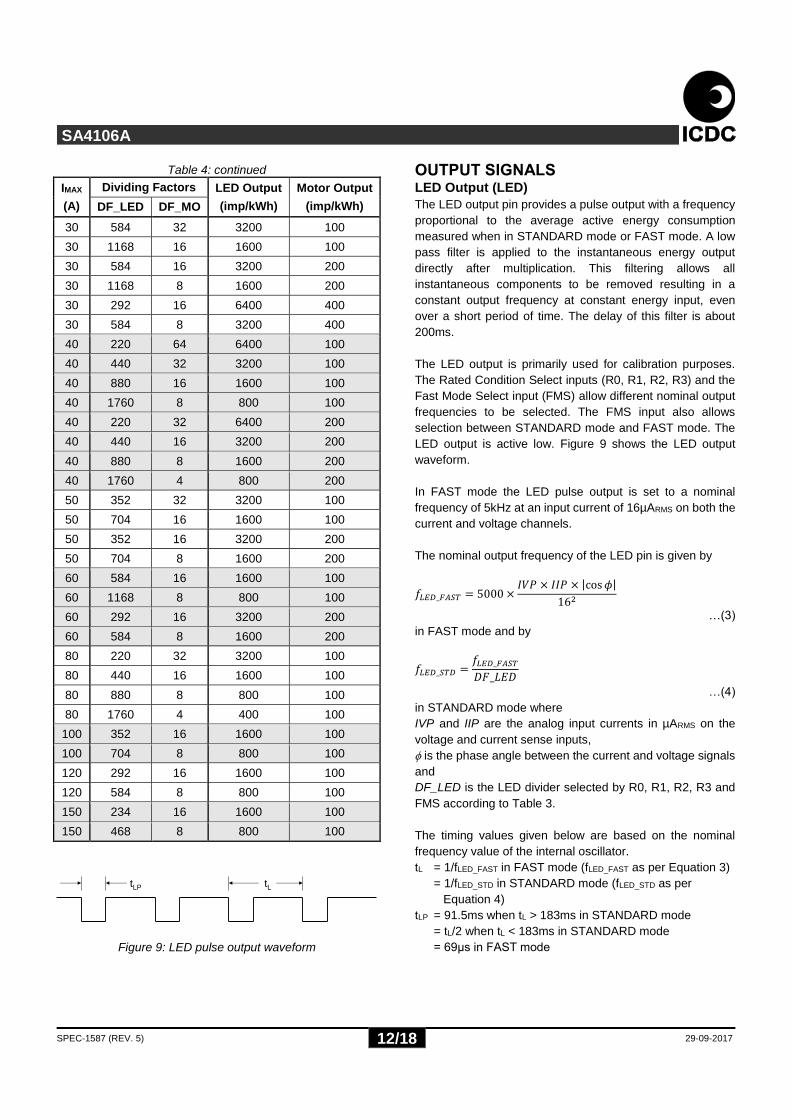
Figure 9: LED pulse output waveform
OUTPUT SIGNALS LED Output (LED)
The LED output pin provides a pulse output with a frequency
proportional to the average active energy consumption
measured when in STANDARD mode or FAST mode. A low
pass filter is applied to the instantaneous energy output
directly after multiplication. This filtering allows all
instantaneous components to be removed resulting in a
constant output frequency at constant energy input, even
over a short period of time. The delay of this filter is about
200ms.
The LED output is primarily used for calibration purposes.
The Rated Condition Select inputs (R0, R1, R2, R3) and the
Fast Mode Select input (FMS) allow different nominal output
frequencies to be selected. The FMS input also allows
selection between STANDARD mode and FAST mode. The
LED output is active low. Figure 9 shows the LED output
waveform.
In FAST mode the LED pulse output is set to a nominal
frequency of 5kHz at an input current of 16µARMS on both the
current and voltage channels.
The nominal output frequency of the LED pin is given by
𝑓𝐿𝐸𝐷_𝐹𝐴𝑆𝑇 = 5000 ×𝐼𝑉𝑃 × 𝐼𝐼𝑃 × |cos 𝜙|
162
…(3)
in FAST mode and by
𝑓𝐿𝐸𝐷_𝑆𝑇𝐷 =𝑓𝐿𝐸𝐷_𝐹𝐴𝑆𝑇
𝐷𝐹_𝐿𝐸𝐷
…(4)
in STANDARD mode where
IVP and IIP are the analog input currents in µARMS on the
voltage and current sense inputs,
is the phase angle between the current and voltage signals
and
DF_LED is the LED divider selected by R0, R1, R2, R3 and
FMS according to Table 3.
The timing values given below are based on the nominal
frequency value of the internal oscillator.
tL = 1/fLED_FAST in FAST mode (fLED_FAST as per Equation 3)
= 1/fLED_STD in STANDARD mode (fLED_STD as per
Equation 4)
tLP = 91.5ms when tL > 183ms in STANDARD mode
= tL/2 when tL < 183ms in STANDARD mode
= 69μs in FAST mode
tLP tL

SPEC-1587 (REV. 5) 13/18 29-09-2017
SA4106A
Motor Pulse Output (MON, MOP)
The MON and MOP pins are complimentary outputs with a
frequency proportional to the average active power
consumption measured. These active high outputs can be
used to either directly drive a stepper motor counter or an
electro-mechanical impulse counter. The Rated Condition
Select inputs (R0, R1, R2, R3) as well as the Fast Mode
Select input (FMS) allow the selection of different output
frequencies corresponding to different meter constants.
Figure 10 indicates the timing of these signals.
The nominal output frequency of each motor output is given
by:
𝑓𝑀𝑂𝑇 =𝑓𝐿𝐸𝐷_𝑆𝑇𝐷
𝐷𝐹_𝑀𝑂
where …(5)
fLED_STD is the output frequency of the LED output in
STANDARD mode as per Equation 4 and
DF_MO is the motor divider selected by R0, R1, R2, R3 and
FMS according to Table 3
When connecting a stepper motor counter between MON and
MOP the output pulse rate is effectively doubled because the
pulses on both MON and MOP contribute to incrementing the
counter.
The timing values given below are based on the nominal
frequency value of the internal oscillator.
tM = 1/fMOT (fMOT as per Equation 5)
tMP = 220ms when tM > 440ms
= tM/2 when tM < 440ms
tMS = tM/2
tMSP = tMS-tMP when tM > 440ms
= 6.7μs when tM < 440ms
Figure 10: Motor pulse output waveform
Anti-Creep State Output (ACST)
The state of the anti-creep circuit is available on the ACST
output pin. This pin allows the state of the anti-creep circuit to
be monitored. A low level on this pin indicates that the anti-
creep circuit has detected an energy level below the
threshold set by the ACSEL pin. In this state no pulses will be
emitted on the LED and the motor pulse outputs. A high level
indicates that the detected energy is above the anti-creep
threshold and pulses will be emitted on the LED and motor
pulse outputs. The ACST pin can be used to drive an LED to
indicate when the SA4106A has detected energy below or
above the anti-creep threshold. A power-on reset will set
ACST low and the pin will go high only once energy above
the anti-creep threshold has been detected. If the anti-creep
threshold is disabled the ACST pin will go high as soon as the
logic low on ACSEL has been detected and it will remain high,
regardless what level of energy is detected.
Direction Indicator Output (DIRO)
The direction of the energy flow may be ascertained by
monitoring the DIRO pin. A low level on this pin indicates
negative energy flow. Positive energy flow is indicated by a
high level. Should the energy (either negative or positive) be
less than the anti-creep threshold then this output will retain
its previous state. This prevents a flickering output in the case
of no or very low current flow. The DIRO pin may be used to
drive an LED. The state of the DIRO pin is updated on the
internal FAST mode pulses, regardless of whether the device
is set to FAST or STANDARD mode and what state DIRI is
set to. A power-on reset will set DIRO high and it will remain
high until negative energy above the anti-creep threshold is
detected. Table 5 illustrates the operation of the DIRO output.
Table 5: Operation of the DIRO output
Energy Level |Phase Angle| State of DIRO
< FMIN 0º - 360º Previous State
> FMIN < 90º HIGH
> FMIN > 90º LOW
Note: FMIN is the anti-creep threshold if enabled
tMP
tMS
tM
tMSPMON
MOP

SPEC-1587 (REV. 5) 14/18 29-09-2017
SA4106A
TYPICAL APPLICATION The following description outlines the basic process required
to design a typical single phase energy meter using the
SA4106A and a shunt resistor as a current sensing element.
The meter is capable of measuring 220V/40A/50Hz with a
precision better than Class 1. It uses a stepper motor counter
with 100imp/kWh and the calibration LED has a constant of
1600imp/kWh.
The most important external circuits required for the
SA4106A are the current input network, the voltage input
network as well as the bias resistor. All resistors should be
1% metal film resistors of the same type to minimize
temperature effects.
Bias Resistor
A bias resistor of R10 = 47k sets optimum bias and
reference currents on chip. Calibration of the meter should be
done using the voltage input and not by means of the bias
resistor.
Current Input Network
The voltage drop across the shunt resistor at maximum rated
current should not be less than 5mVRMS and not exceed
100mVRMS. A 320μ shunt is chosen which sets the voltage
drop at maximum rated current to 12.8mV and the maximum
power dissipation in the shunt to 0.5W. The voltage across
the shunt resistor is converted to the required differential
input currents through the current input resistors. Anti-alias
filters are incorporated on these input resistors to filter any
high frequency signal components that could affect the
performance of the SA4106A.
The four current input resistors (R1, R2, R3, R4) should be of
equal size to optimize the input networks low pass filtering
characteristics, so the values can be calculated as follows:
𝑅1 = 𝑅2 = 𝑅3 = 𝑅4 = 𝐼𝑀𝐴𝑋 ×𝑅𝑆𝐻
4 × 16𝜇𝐴= 200Ω = 𝑅𝐶
For optimum performance the cut-off frequency of the anti-
alias filter should be between 10kHz and 20kHz. The
equivalent resistance associated with each capacitor is RC/2
so the capacitor values should be in the order of
𝐶1 = 𝐶2 =1
𝜋𝑓𝐶𝐼𝑅𝐶=
1
𝜋 × 15𝑘𝐻𝑧 × 200Ω≈ 100𝑛𝐹 = 𝐶𝐶
where fCI is the cut-off frequency of the anti-alias filter of the
current input network.
Voltage Input Network
The voltage sense input requires an input current of 11μARMS
at VNOM (220V) according to Table 1. The mains voltage is
divided by means of a voltage divider to a lower voltage that
is converted to the required input current by means of the
input resistor. Once again an anti-alias filter is required to
remove any high frequency signals that could affect the
performance of the SA4106A. A shunt typically has very little
phase shift so phase compensation is not required.
The input resistor R8 sets the current input into the device.
This resistor should not be too large else the capacitor for the
anti-alias filter will be quite small which could cause
inaccurate phase shift due to parasitic capacitances.
Therefore R8 = 100k is chosen and the voltage at the centre
of the trimpot should be 1.1V (11μA x 100k). The calibration
range of the voltage input network should be about ±15% to
ensure that all component tolerances can be catered for, so
the total tuning range can be set to ±0.17V. Therefore the
voltage across the trimpot and R9 is 1.27V. Choosing a 1k
trimpot results in:
𝑅9 =1𝑘Ω
(2 × 0.17)× (1.27 − 2 × 0.17) ≈ 2.7𝑘Ω
The effect of R8 can be ignored in the above equation, given
the fact that R8 is significantly larger than P1 and R9. Now let
RA = R5 + R6 + R7 and
𝑅𝐴 = (𝑃1 + 𝑅9) × (220𝑉
1.27𝑉− 1) ≈ 637𝑘Ω
so choose R5 = 240k, R6 = 220k and R7 = 180k.
The cut-off frequency of the anti-alias filter is adjusted so that
it is identical to that of the current input network anti-alias
filters. This ensures that the phase shift caused by the anti-
alias filters is identical on the current and voltage input
networks. Therefore
1
𝜋𝐶𝐶 × 𝑅𝐶=
1
2𝜋(𝑃1 + 𝑅9) × 𝐶3
and so C3 = 2.7nF.

SPEC-1587 (REV. 5) 15/18 29-09-2017
SA4106A
Device Setup
The SA4106A has to be set to STANDARD mode. Using
Equations 1 and 2 in the Rated Condition Select section the
required LED and motor dividers for 1600imp/kWh and
100imp/kWh respectively are calculated as DF_LED = 880
and DF_MO = 16. Using Table 3 the device is set up using
FMS = VSS, R3 = VDD, R2 = VSS, R1 = VDD and R0 = VSS.
The lowest possible creep limit is chosen to allow the meter
to register energy at very low currents, so ACSEL is left
floating. In order to obtain the highest immunity against
tampering the SA4106A is set up to measure bidirectional
energy by connecting DIRI to DIRO.
Figure 11: Typical application circuit
Table 6: Component list for typical application
Symbol Description
U1 Energy metering device, SA4106ASAR
U2 Opto-coupler, 1N35
RSH Shunt Resistor, 40A, 320μ
R1, R21, R3,
R41 Resistor, 200, 1%, metal film
R5 Resistor, 240k, 1%, metal film
R6 Resistor, 220k, 1%, metal film
R7 Resistor, 180k, 1%, metal film
R81 Resistor, 100k, 1%, metal film
R9 Resistor, 2.7k, 1%, metal film
R101 Resistor, 47k, 1%, metal film
R11 Resistor, 680, 5%, carbon film
R12, R13 Resistor, 100, 5%, carbon film
Symbol Description
R14, R15 Resistor, 1k, 5%, carbon film
P1 Trim-pot, 25 turns, 1k
C1, C2 Capacitor, 100nF, ceramic
C3 Capacitor, 2.7nF, ceramic
C42, C52 Capacitor, 220nF, ceramic
C62 Capacitor, 1μF, ceramic
D1 Light emitting diode, pulse output
D2 Light emitting diode, anti-creep state
output
D3 Light emitting diode, energy direction
output
CNT1 Stepper motor counter, 100imp/kWh
Note 1: Resistors R2, R4, R8 and R10 must be positioned as close as possible to the respective device pins
Note 2: Capacitors C4, C5 and C6 must be positioned as close as possible to the VDD and VSS power supply pins
8
14
3
VDD
VSS
VREF
IIP
IIN
SA4106A
U1
LED
MON
MOP
IVP
AGND20
19
12
15
13
2
1
C2
R3 R4
R1 R2
200 200
200 200
C1 100nF
100nF
R10
47k-2.5V
+2.5V
R5
240k
R6
220k
R7
180k
R8
100k
P1 1k R9
2.7k
0V
0V
R13
100
R12
100
CNT1
7 6 5 4 3 2 . 1
D1
Pulse
+2.5V
R11
680
Pulse Out
U2
4N35
LIVE IN
NEUTRAL
0V
LIVE OUT
C32.7nF
0V
C4
220nF
C5
220nF
C6
1µF
+2.5V
-2.5V
0V
RSH
320µ0V
ACST16 R14
1k
D2
Creep
DIRO17 R15
1k
D3
Direction
+2.5V
R1
R3
5
11
6R0
R2
FMS
4
7
-2.5V
+2.5V
ACSEL9
DIRI18

SPEC-1587 (REV. 5) 16/18 29-09-2017
SA4106A
PACKAGE DIMENSIONS
SOIC20 Package Dimensions are shown in inches

SPEC-1587 (REV. 5) 17/18 29-09-2017
SA4106A
NOTES

SPEC-1587 (REV. 5) 18/18 29-09-2017
SA4106A
DISCLAIMER The information contained in this document is confidential and proprietary to Integrated Circuit Design Centre (Pty) Ltd ("ICDC"),
a division of South African Micro-Electronic Systems (Pty) Ltd ("SAMES"), and may not be copied or disclosed to a third party, in
whole or in part, without the express written consent of ICDC. The information contained herein is current as of the date of
publication; however, delivery of this document shall not under any circumstances create any implication that the information
contained herein is correct as of any time subsequent to such date. ICDC does not undertake to inform any recipient of this
document of any changes in the information contained herein, and ICDC expressly reserves the right to make changes in such
information, without notification, even if such changes would render information contained herein inaccurate or incomplete. ICDC
makes no representation or warranty that any circuit designed by reference to the information contained herein, will function
without errors and as intended by the designer.
Any sales or technical questions may be sent to our support e-mail address:
For the latest updates on datasheets, please visit our web site:
http://www.sames.co.za.
INTEGRATED CIRCUIT DESIGN CENTRE (PTY) LTD
a division of
SOUTH AFRICAN MICRO-ELECTRONIC SYSTEMS (PTY) LTD
Tel: 012 333 6021
Tel Int: 00 27 12 333 6021
Fax: 012 333 6393
Fax Int: 00 27 12 333 6393
PO BOX 15888
LYNN EAST 0039
REPUBLIC OF SOUTH AFRICA
UNIT 4, PERSEQUOR CLOSE
49 DE HAVILLAND CRESCENT
PERSEQUOR TECHNOPARK
LYNNWOOD, PRETORIA
REPUBLIC OF SOUTH AFRICA