Embed Size (px)
Citation preview
FEASIBILITY STUDY OF SECONDARY EMISSION ELECTRON MICROSCOPY FOR EXAMINING MATERIALS CONTAINING DISPERSED OXIDE PARTICLES
by L. Fredrick Norris und Wulter S. Cremens
Lewis Research Center CZeveZand, Ohio
I
1 N A T I O N A L AERONAUTICS AND SPACE A D M I N I S T R A T I O N WASHINGTON, D. C . OCTOBER 1966
i f
https://ntrs.nasa.gov/search.jsp?R=19660028388 2018-08-20T12:53:45+00:00Z
TECH LIBRARY KAFB. NM
0330257 NASA TN D-3650
FEASIBILITY STUDY O F SECONDARY EMISSION ELECTRON
MICROSCOPY FOR EXAMINING MATERIALS CONTAINING
DISPERSED OXIDE PARTICLES
By L. F r e d r i c k N o r r i s and Wal t e r S. C r e m e n s
Lewis R e s e a r c h Center Cleveland, Ohio
N A T I O N A L AERONAUTICS AND SPACE ADMINISTRATION
For sale by the Cleoringhouse for Federal Scientific and Technical Information Springfield, Virginia 22151 - Price 62.00

CONTENTS
Page SUMMARY . . . . . . . . . . . . . . . . . . . . . . . . . . . . . . . . . . . . . . . . 1
INTRODUCTION . . . . . . . . . . . 2
SECONDARY EMISSION ELECTRON MICROSCOPY . . . . . . . . . . . . . . . . . . 3
APPARATUS. MATERIALS. AND PROCEDURES . . . . . . . . . . . . . . . . . . . . 5 Description of Secondary Emission Electron Microscope (SEEM) . . . . . . . . . . 5 Operation of SEEM . . . . . . . . . . . . . . . . . . . . . . . . . . . . . . . . . . 7 Materials Examined . . . . . . . . . . . . . . . . . . . . . . . . . . . . . . . . . . 8 Specimen Preparation for SEEM Examination . . . . . . . . . . . . . . . . . . . . 10 Replication for Conventional Electron Microscopy . . . . . . . . . . . . . . . . . . 10 Particle Sizing and Counting . . . . . . . . . . . . . . . . . . . . . . . . . . . . . 10 Determination of SEEM Resolution Limit . . . . . . . . . . . . . . . . . . . . . . 11 Experiments for Explanation of "Volume Percent Anomaly'' . . . . . . . . . . . . 11 Investigation of Phase Discrimination . . . . . . . . . . . . . . . . . . . . . . . . . 11
RESULTS . . . . . . . . . . . . . . . . . . . . . . . . . . . . . . . . . . . . . . . . . 12 Secondary Electron Emission Microscope . . . . . . . . . . . . . . . . . . . . . . 12 Particle Size and Particle Image Enlargement . . . . . . . . . . . . . . . . . . . . 18 Results of Experiments to Determine Ion Beam Penetration . . . . . . . . . . . . 30 Results of Investigation into Irregular Ion Beam Etching . . . . . . . . . . . . . . . 30 Phase Discrimination inOxide/Oxide and Metal/MetalSystems . . . . . . . . . . . 31 Other Practical Examples of Dispersion Microstructures Viewed by SEEM and by CEM . . . . . . . . . . . . . . . . . . . . . . . . . . . . . . . . . 35
Nickel-base alloys . . . . . . . . . . . . . . . . . . . . . . . . . . . . . . . . . . 35 Aluminum -base alloys . . . . . . . . . . . . . . . . . . . . . . . . . . . . . . . 36 Tungsten-base alloys . . . . . . . . . . . . . . . . . . . . . . . . . . . . . . . . 36
DISCUSSION . . . . . . . . . . . . . . . . . . . . . . . . . . . . . . . . . . . . . . . 42 Resolution and Detection Limits of SEEM . . . . . . . . . . . . . . . . . . . . . . . 42 Distortion - Preferential Enlargement of Oxide-Particle Images . . . . . . . . . . 43 Phase Discrimination . . . . . . . . . . . . . . . . . . . . . . . . . . . . . . . . . 44
CONCLUSIONS . . . . . . . . . . . . . . . . . . . . . . . . . . . . . . . . . . . . . . 45
APPENDIX . QUALITATIVE EVIDENCE FOR IMAGE DISTORTION . . . . . . . . . . 47 REFERENCES . . . . . . . . . . . . . . . . . . . . . . . . . . . . . . . . . . . . . . 48
I
FEASIBILITY STUDY OF SECONDARY EMISSION ELECTRON
MICROSCOPY FOR EXAMINING MATERIALS CONTAINING
DISPERSED OXIDE PARTICLES
by L. Fredrick Norris and Walter S. Cremens
Lewis Research Center
SUMMARY
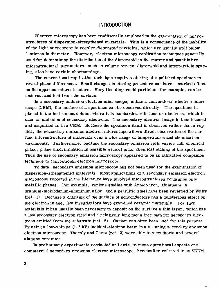
The feasibility of using a secondary emission electron microscope (SEEM) to examine dispersion-strengthened materials was explored. Nickel, tungsten, and aluminum con- taining submicron oxide dispersoids were examined and the results compared with micro- graphs from a conventional electron microscope. Because secondary electron emission varies with chemical phase, separate phases, such as metal and oxide in a microstruc- ture, can be differentiated because of different levels of brightness in the image.
in most of the materials examined, but an unexpected preferential enlargement of oxide particle images was discovered, which precluded the anticipated use of the SEEM for measurement of microstructural parameters. The image enlargement gives rise to a deteckion limit of 350 A (0.035 p ) for thoria particles in a nickel matrix, which value lies well below the measured resolution limit of 800 A (0.08 p ) .
Various levels of image brightness were also observed in a composite foil laminate of several metals. Phase discrimination between metals and between oxides was found to be limited to those combinations having substantially different yields of secondary electrons. However, discrimination between two different oxides in a metal matrix was not achieved under the various experimental conditions used.
For the specific purpose of examining ultrafine oxide dispersion microstructures, secondary emission electron microscopy does not provide important advantages over conventional electron microscopy. There are other applications, however , where the distortion associated with oxides may not limit the use of secondary emission micro- scopes.
A high metal/oxide contrast, desirable for quantitative metallography, was observed
INTRO D UCTlON
Electron microscopy has been traditionally employed in the examination of micro- structures of dispersion-strengthened materials. This is a consequence of the inability of the light microscope to resolve dispersoid particles, which are usually well below 1 micron in diameter. However , electron microscopy replication techniques generally used for determining the distribution of the dispersoid in the matrix and quantitative microstructural parameters, such as volume percent dispersoid and interparticle spac- ing, also have certain shortcomings.
The conventional replication technique requires etching of a polished specimen to reveal phase differences. Small changes in etching procedure can have a marked effect on the apparent microstructure. Very fine dispersoid particles, for example, can be undercut and lost from the surface.
In a secondary emission electron microscope, unlike a conventional electron micro- scope (CEM), the surface of a specimen can be observed directly. The specimen is placed in the instrument column where it is bombarded with ions or electrons, which in- duce an emission of secondary electrons. The secondary electron image is then focused and magnified as in a CEM. Because the specimen itself is observed rather than a rep- lica, the secondary emission electron microscope allows direct observation of the sur- face microstructure of materials over a wide range of temperatures and chemical en- vironments. Furthermore, because the secondary emission yield varies with chemical phase, phase discrimination is possible without prior chemical etching of the specimen. Thus the use of secondary emission microscopy appeared to be an attractive companion technique to conventional electron microscopy.
dispersion-strengthened materials. Most applications of a secondary emission electron microscope reported in the literature have involved microstructures containing only metallic phases. For example, various studies with Armco iron, aluminum, a uranium-molybdenum-aluminum alloy, and a pearlitic steel have been reviewed by Watts (ref. 1). Because a charging of the surface of nonconductors has a deleterious effect on the electron image, few investigators have examined ceramic materials. For such materials it has usually been necessary to deposit on the surface a thin layer, which has a low secondary electron yield and a relatively long mean free path for secondary elec- trons emitted from the substrate (ref. 2). Carbon has often been used for this purpose. By using a low-voltage (1.5 kV) incident-electron beam in a scanning secondary emission electron microscope, Thornly and Cartz (ref. 3) were able to view thoria and several alumina ceramics.
In preliminary experiments conducted at Lewis, various operational aspects of a commercial secondary emission electron microscope, hereinafter referred to as SEEM,
To date, secondary emission microscopy has not been used for the examination of
2

were investigated. Examination of a dispersion of coarse thoria particles in a tungsten matrix yielded micrographs characterized by extremely high oxide/matrix contrast. Specimens containing submicron oxide dispersoids in nickel also exhibited high contrast; however, quantitative metallography of micrographs of both materials revealed a major problem. It was found that the area fraction of oxide dispersoid observed in the micros- graphs was larger than the volume percent oxide known to be present in the sample. This "volume percent anomaly" necessarily became a subject of study since distorted values were obtained for microstructural parameters.
copy for the examination of dispersion-strengthened materials. In particular, the fea- sibility of using the SEEM for determining quantitative microstructural parameters (particle size, volume percent dispersoid, interparticle spacing) was to be determined by examining dispersion-strengthened materials with particle sizes and interparticle spac- ings of less than 1 micron. Comparison could then be made between parameters deter- mined by the SEEM and by a CEM. In addition, the sensitivity of phase discrimination was to be determined. An indication of whether the SEEM could be used to reveal the presence of additional metallic phases in a dispersion-strengthened alloy microstructure was also expected. the matrix in a metal/oxide dispersion product, that is, discriminating between two :;if- ferent oxide phases, was also to be determined.
Several dispersion-strengthened materials were examined in the SEEM and in a CEM under controlled conditions. These included three tungsten-thoria alloys, a nickel-thoria alloy (TD-Nickel), two nickel-alumina alloys, an aluminum-alumina alloy (Alcoa M-257), and a nickel - nickel oxide - alumina alloy. The last alloy and a multilayer foil laminate were used for part of the investigation of phase discrimination. The microstructures of tungsten-thoria and nickel-thoria alloys were utilized for quantitative metallography in solving the volume percent anomaly. Two unidirectionally solidified eutectics were also used, one in the measurement of the resolution limit of the SEEM, the other to reveal the ion-etching capabilities of the instrument.
This study explored the possibilities of utilizing secondary emission electron micros-
The possibility of detecting contamination consisting of an oxide of
SECONDARY EM1 S S ION ELECTRON MICROSCOPY
The theory and practice of electron emission microscopy have been reviewed recently by Moellenstedt and Lenz (ref. 2). Emission microscopy is characterized by the emission of imaging electrons directly from the specimen-cathode. tradistinction to reflection electron microscopy and electron mirror microscopy, where- in an external source of electrons is necessary (although the specimen itself is ob- served). The methods of inducing electron emission in emission microscopy include
This is in con-
3
photoemission, electron emission under ion, atom, or molecular bombardment, thermi- onic emission, and field emission.
Kaminsky (ref. 5). The physical basis for secondary emission microscopy is the yield of secondary electrons, that is, the number of secondary electrons emitted per incident primary electron or ion. The yield is a function of the target material and its crystal- lographic orientation, the angle of incidence of the primary ion beam, the ion species, ion discharge potential, and, to some extent, the target temperature.
Two types of microscopes based on secondary electron emission have been developed In one, a complete image of the cathode is formed at every instant on either a fluorescent screen or a photographic plate. A cone of ions sprayed onto the specimen by an ion gun induces the emission of secondary electrons, which is focused with a lens system. The instrument (SEEM) used in this study is an example.
In a second type, the specimen surface is scanned with a very small diameter elec- tron beam. The secondary electrons emitted are used to control the intensity of a syn- chronized beam scanning a display tube. No lenses are used to focus the complete image. Scanning microscopes have recently been made available commercially by Cambridge Instrument Company, Ltd., of England and by Westinghouse Electric Instrument Corpora- tion.
electron microscopes and optical microscopes. The scanning secondary-emission micro- scopes have been reported by the manufacturers to have a resolving power (100 to 600 A) somewhat superior to the SEEM (500 to 1000 A). The depth of field of the scanning secondary-emission microscope is also greater than that of the SEEM; thus relatively irregular surfaces can be examined.
The physics of secondary-electron emission has been treated by Bruining (ref. 4) and
Both types of instruments have resolving powers intermediate between conventional
Microstructural details in micrographs obtained with a SEEM arise in two different ways. The differences in secondary emission yields from various chemical phases may be sufficient to permit discrimination between these phases by differences in their bright- ness levels. Secondly, surface structures present initially from prior etching or devel- oped by ion etching during observation a re revealed by their topography.
With a specimen consisting of two phases, such as a metal and its oxide, the differ- ences in secondary electron emission between the phases, observed as differences in levels of brightness, allow these phases to be distinguished. The emission current from several metals of relevance to the present study are Listed in table I (obtained from ref. 6) for different types of discharge ions. to choose the bombarding ion so that maximum separation of the phases can be effected in the specimen on the basis of image intensity.
From such a tabulation it should be possible
Because the ion beam illuminates the specimen at shallow angles to the surface,
4
I
TABLE I. - EMISSION CURRENT I N NANOAMPERES FOR VARIOUS TARGET
MATERIALS AND IONS
[Specimen temperature, 300' C; discharge current, 50pA; discharge voltage, 25 kV; data from ref. 6. ]
Target material
Ions
Hydrogen Argon Nitrogen Oxygen A i r
- Aluminuma
160 57 90
105 90
Zirconium
100 66 52 60 54
aEmission enhanced by oxide layer.
Carbo:
40 28 23 22 24.5
ritanium
38 23 17.5 28 20
rantalum
28 17 17 19 18
Tungsten
24 13 14 14 15
10 .5
10.5 50
topogra, iical features of the surface are c-:arly revealec. At the highest angles [about 20') the rough features of the surface are emphasized while at the lowest angles (about 2') fine details become visible. Either high ion beam currents or long observation at low currents results in etching of the surface. Grain boundaries, deformation twins, and other surface features usually revealed in chemical etching are then displayed (ref. 1).
APPARATUS, MATERIALS, AND PROCEDURES
Description of Secondary Emission Electron Microscope (SEEM)
The secondary emission electron microscope used in this study is of the Moellenstedt- Dueker design and is commercially available from B a k e r s of Liechtenstein as the Metioscope (referred to as SEEM herein). A cross section through the vacuum column of the instrument is shown in figure l(a). An inverted specimen, serving as the cathode, is bombarded by positive ions from the ion gun, which may be adjusted to various angles of impingement (2' to 20'). The secondary electrons emitted from the specimen are focused and accelerated by an electrostatic immersion objective consisting of the cathode, Wehnelt (direct-current control electrode), and anode. The image passes through an aperture and two magnetic lenses to the fluorescent screen or photographic plates for observation. A detailed schematic of the imaging components is given in figure l(b). A telescope is used in final focusing. A tungsten wire resistance heater surrounding the specimen base allows heating to llOOo C. Temperature is measured by a thermocouple imbedded in the specimen base. change the area of the specimen viewed. Gases for a controlled chemical environment
The specimen head can be rotated or translated to
5
I
Specimen rl , y",,~( ;e; ,~ ,-Specimen rotation
r S p e c i m e n heater
(control electrode)
Fluorescent screen
-V
/ - :;;: ' ." ;, Ion beam ,,- ,::: . ?$:. . . Control electrode
:. . , .::' (We h ne1 t) . . . ,', . . . .
/ /
L5ssSx3 - V t A V
-4- - \'
Emitted secondary electrons
; Fluorescent screen
- - - CD-8396 ' '
(a) Sectional view of SEEM vacuum column. (b) Detailed schematic of principal components in image-forming section.
Figure 1. - Sectional view of vacuum column and detailed schematic of image-forming section of secondary emission electron microscope (SEEM).
can be admitted through a valve into the vacuum column.
Not shown in figure l(a) is the vacuum pumping system. The column is evacuated by a two-stage rotary pump coupled with a baffled three-stage oil diffusion pump and liquid-nitrogen cold trap. The photographic plate cassette air lock is evacuated by a separate rotary pump. Column vacuum is measured by a cold-cathode gage.
Thermocouple well For the present study, the SEEM speci- men was modified to serve as a specimen holder, as shown in figure 2. The materials to be examined, generally in the shape of small
holders, and then polished. 1 0 1 2 pellets, were machined, mounted in these l f l l l b l i , i , L I 1
cm
Figure 2. - Specimen holder and wedge-shaped specimen for SEEM.
Operation of SEEM
In common with conventional electron microscopes, the SEEM has basic operational features, such as evacuation of the column and alignment of the electron optics. With liquid nitrogen trapping, initial column pressures of to torr were achieved. During normal operation (with an ion beam current of 25 pA), the column pressure was of the order of 2 ~ l O - ~ torr .
Heating of the specimen was not generally necessary for the development of contrast between brightness levels of the metal and oxide phases. Exceptions were alloys contain- ing thoria for which heating to the range of 400' to 500' C resulted in a marked increase in oxide/metal contrast over that at room temperature. However, most specimens in this study were run in the temperature range 50' to 500' C to reduce contamination by organic residues from sources such as diffusion pump oil. temperatures, high voltage discharges, which contaminated the Wehnelt and anode, were minimized. Specimen heating rates of the order of 80' to 100' C per minute were em- ployed.
Both the ion discharge potential and the ion beam current in the SEEM can be con- trolled over ranges of 9 to 18 kilovolts and 0 to 100 microamperes, respectively. In practice, the discharge potential is fixed for a given experiment, and the ion current is varied in the range 25 to 50 microamperes for general observation or to 100 microamperes
By outgassing at somewhat elevated
7

if ion etching and simultaneous observation are desired. With the higher ion currents, ion etching is accompa'nied by erosion of the specimen surface along the direction of the beam. To simplify interpretation of the microstructure, it is therefore important to make observations quickly and to use ion beam currents as low as practicable, usually about 25 microamperes. Undesirable erosion of the specimen surface can also be mini- mized by using a light gas (such as hydrogen or helium) in the ion source and by using low ion potentials.
Materials Examined
Materials examined in this study are listed in table II. The main subjects of exami- nation were dispersion alloys with matrices of nickel, aluminum, and tungsten containing dispersions of thoria, alumina, or zirconia. Some all-metal composite materials, a foil laminate and two unidirectionally solidified eutectics, were included to illustrate particular points.
The most intensive study was done on TD-Nickel, nickel containing a fine dispersion of thoria, with a particle size range which was known to bracket the suspected resolution of the SEEM. The particular specimen used was a bar, identified as 53B, which was produced by du Pont during their early commercialization of the material. The bar was annealed at llOOo C for 1 hour in vacuum prior to examination. This material had an average particle size of about 0.03 micron, whereas currently produced TD-Nickel is said to have a finer particle size, of less than 0.02 micron (unpublished data from W. Pollock of du Pont).
Other nickel alloys examined were three compacted blends of nickel and alumina powders. One of the blends also had an admixture of nickel oxide. Two of the compacted blends were selected out of a large number which were examined in the SEEM as part of a study of blending techniques. For both blends, alumina of particle size 0.02 micron was used, but the nickel powder particle sizes were different, being 1 to 2 microns for one and 0.02 micron for the other. These two specimens were chosen to demonstrate the use of the SEEM as a screening test for evaluating blends of metal and oxide powders.
combinations of ion species, discharge voltages, and specimen temperatures in the SEEM to determine whether fine alumina could be distinguished from fine nickel oxide.
The aluminum alloy M-257, containing a nominal 5 weight percent of alumina, was included as representative of the sintered aluminum powder type.
The three tungsten-base alloys came from current work a t Lewis. Tungsten with coarse thoria particles was chosen to illustrate the sharp, high-contrast pictures obtain- able in the SEEM when particles are well above the resolution limit. Tungsten with fine thoria and a tungsten-tantalum alloy were examined in the SEEM because earlier examina- tion by etching, replication, and the use of the CEM had not given micrographs in which
A blend of nickel, nickel oxide, and alumina was made for exposure to a number of
8
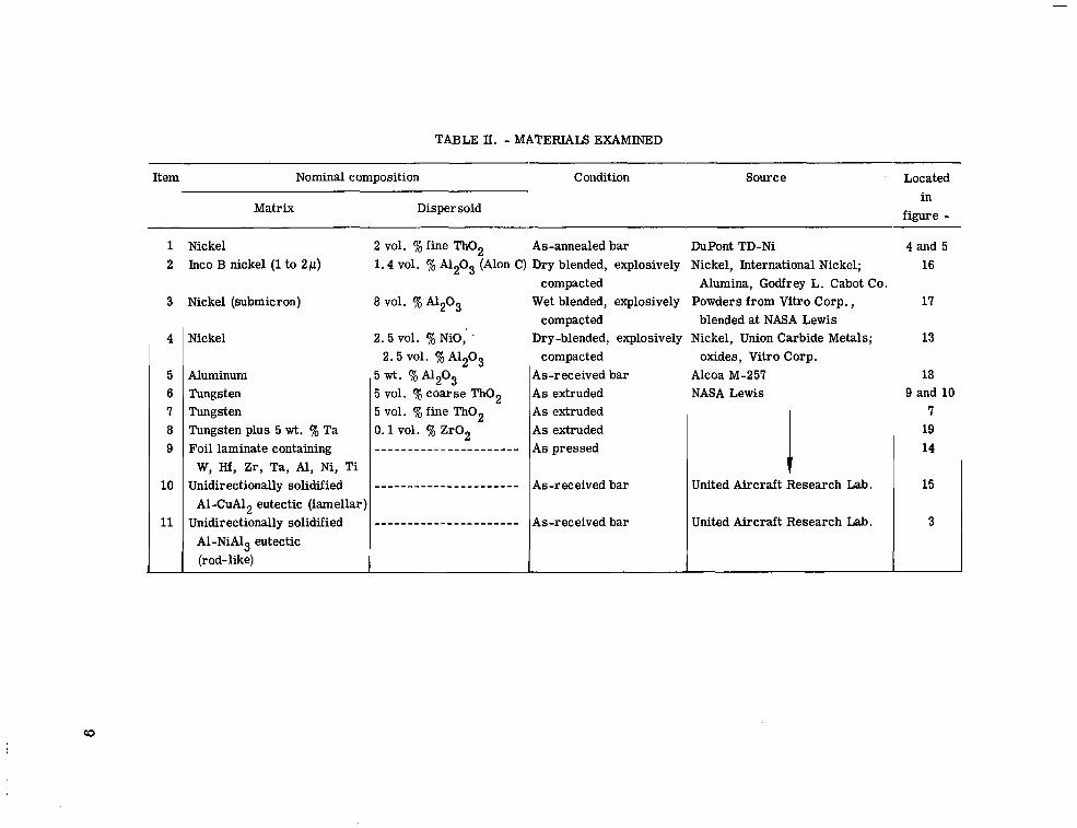
TABLE II. - MATERIALS EXAMINED
Located in
figure -
Item Nominal composition Condition Source
Dispersoid Matrix
1 2
3
4
5 6 7 8 9
10
11
Nickel Inco B nickel (1 to 2 p )
Nickel (submicron)
Nickel
Aluminum Tungsten Tungsten Tungsten plus 5 wt. % Ta Foil laminate containing
Unidirectionally solidified
Unidirectionally solidified
W, Hf, Z r , Ta, Al, Ni, Ti
A1-CuA12 eutectic (lamellar)
A1-NiA13 eutectic (rod-like)
2 vol. %fine Tho2 As-annealed bar DuPont TD-Ni 1.4 vol. % A1203 (Alon C) Dry blended, explosively Nickel, International Nickel;
compacted 8 V O ~ . % A1203
compacted blended at NASA Lewis 2 . 5 ~ 0 1 . %NiO, '
Alumina, Godfrey L. Cabot Co. Wet blended, explosively Powders from Vitro Corp.,
Dry-blended, explosively Nickel, Union Carbide Metals; compacted oxides, Vitro Corp.
As-received bar Alcoa M-257 A s extruded NASA Lewis A s extruded A s extruded A s pressed
As-received bar
A s -r eceived bar
United Aircraft Research Lab.
United Aircraft Research Lab.
4 a n d 5 16
17
13
18 9 and 10
7 19 14
15
3
phases were clearly distinguished.
nickel, and aluminum was prepared to show their relative "brightness" in the SEEM (for one operating condition).
The unidirectionally solidified eutectics, A1-CuA12 and A1-A13Ni were included to illustrate the appearance of two -phase all-metal microstructures and to allow measure - ments to be made on them for calculation of resolution limit.
A composite metal foil laminate of titanium, zirconium, tantalum, hafnium, tungsten,
Specimen Preparation for SEEM Examination
Preparation for fully dense materials, such as extruded bar stock and unidirectionally solidified eutectics, involved mounting in a specimen holder followed by polishing accord- ing to the following procedure. Materials received as powders were explosively com- pacted in a cartridge-actuated compaction press (ref. 7) and then mounted and polished. Only specimens whose density was in excess of 85 percent of theoretical were examined in this study. The foil laminate was prepared by encapsulating various metal foils in aluminum foil. After the capsule was imbedded in a conducting mounting powder and pressed in a metallographic mounting press, it was sectioned, cut to f i t a specimen holder, and then polished.
After the specimens were mounted in SEEM specimen holders, all samples were polished according to the following sequence: papers through number 600, white silk satin with 3-micron diamond compound, and gama1 cloth with 1/4-micron diamond com- pound. Polishing debris was removed by repeated alcohol washings. With compacts of relatively low density, ultrasonic cleaning of the polished specimens was found to be desirable.
Replication for Conventional Electron Microscopy
Replication was used in obtaining conventional electron micrographs. The preceding polishing procedure for specimens was followed and after etching with an appropriate etchant, two-stage carbon-Mowital replicas were prepared. Replicas were shadowed with urania. A Philips Electron Microscope (Model EM100B) was used.
Particle Sizing and Counting
A Zeiss Particle Size Analyzer (model TGZ-3), which can be used to record data on either a distributive or cumulative basis, was used to count and size dispersoid particles on electron micrographs (ref. 8). The "particles" so counted represent intercepts of
10
, .. . ~- . ..
I
the plane of polish with the three-dimensional dispersoid particles in the original speci- men. Throughout this paper, the two-dimensional intercepts observed in the micrographs will be referred to simply as particles.
The size distributions of particles were measured in micrographs of TD-Nickel and a tungsten-thoria dispersion alloy both as observed in the SEEM and in a conventional electron microscope. To insure that sufficient particles were counted to reduce effects of local inhomogeneities in the oxide distribution, several micrographs of each specimen were generally used. For example, 3 SEEM micrographs and 10 CEM micrographs of TD-Nickel were measured. These data were used to measure the preferential enlarge- ment of oxide particle images occurring in the SEEM.
Determination of SEEM Resolution Limit
In this study the resolution limit is defined as the minimum separation between two microstructural features clearly distinguishable as such in a photomicrograph. To avoid the distortion found in oxide images (which will be discussed in the following section), an all-metal system was examined. A rodlike unidirectionally solidified eutectic, supplied by United Aircraft Research Laboratories, was chosen on the basis of its unusually uni- form microstructure. Although the "rods" and their spacing proved to be too large to use directly, the separation of fine topographic features in the etched microstructure could be used to determine the resolution limit.
Experiments for Explanation of V o l u m e Percent Anomaly"
To determine the nature of the volume percent anomaly, a comparison was made between the particle densities (number of particles per unit area) and sizes measured by secondary emission microscopy and by conventional electron microscopy (replication). When it was determined that there was a selective enlargement of oxide particle images, particle sizing and counting measurements were made to explore the variability of this enlargement and to establish enlargement factors for selected materials.
to the specimen and the ion beam etching rate contributed to the volume percent anomaly. Additional experiments were run to determine whether penetration of the ion beam in-
Investigation of Phase Discrimination
In this study phase discrimination is defined as the ability to distinguish between two distinct phases in a microstructure. Three classifications of phase discrimination were investigated: metal/oxide, oxide/oxide, and metal/metal. Dispersions of alumina, thoria, and nickel oxide in nickel; thoria and zirconia in tungsten; and alumina in alumi-
11
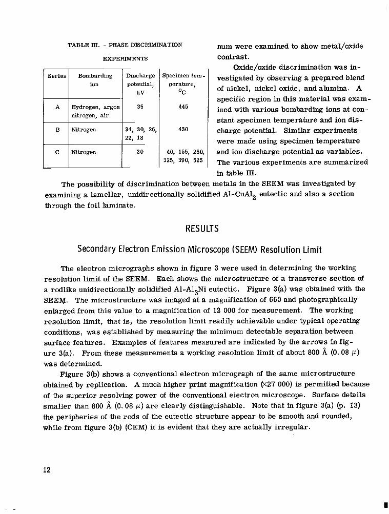
TABLE III. - PHASE DISCRIMINATION
Series Bombarding Discharge ion potential,
kV
A Hydrogen, argon
34, 30, 26, 22, 18
nitrogen, air
B Nitrogen
C Nitrogen
EXPERIMENTS
40, 155, 250,
Specimen tem- perature,
OC
445
430
num were examined to show metal/oxide contrast.
Oxide/oxide discrimination was in- vestigated by observing a prepared blend of nickel, nickel oxide, and alumina. A specific region in this material was exam- ined with various bombarding ions at con- stant specimen temperature and ion dis- charge potential. Similar experiments were made using specimen temperature and ion discharge potential as variables. The various experiments are summarized in table IU.
The possibility of discrimination between metals in the SEEM was investigated by examining a lamellar, unidirectionally solidified A1-CuA12 eutectic and also a section through the foil laminate.
RESULTS
Secondary Electron Emission Microscope (SEEM) Resolution Limit
The electron micrographs shown in figure 3 were used in determining the working resolution limit of the SEEM. Each shows the microstructure of a transverse section of a rodlike unidirectionally solidified A1-A13Ni eutectic. Figure 3(a) was obtained with the SEEM. The microstructure was imaged at a magnification of 660 and photographically enlarged from this value to a magnification of 12 000 for measurement. The working resolution limit, that is, the resolution limit readily achievable under typical operating conditions, was established by measuring the minimum detectable separation between surface features. Examples of features measured are indicated by the arrows in fig- ure 3(a). From these measurements a working resolution limit of about 800 A (0.08 p) was determined.
obtained by replication. A much higher print magnification (X27 000) is permitted because of the superior resolving power of the conventional electron microscope. Surface details smaller than 800 A (0.08 1-1) are clearly distinguishable. Note that in figure 3(a) (p. 13) the peripheries of the rods of the eutectic structure appear to be smooth and rounded, while from figure 3(b) (CEM) it is evident that they are actually irregular.
Figure 3(b) shows a conventional electron micrograph of the same microstructure
12
I
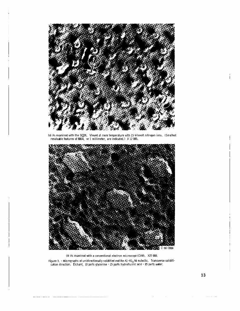
(a) As examined w i th t h e SEJM. Viewed at room temperature w i th 15-kilovolt n i t rogen ions. ISmallest resolvable features of NOA, or 1 mil l imeter, a re indicated.) X 12 000.
(b) As examined wi th a conventional electron microscope (CEM). X27 OOO.
Figure 3. - Micrographs of un id i rect ional ly solidified rodl ike A1-A13Ni eutectic. Transverse solidif i- cation direct ion. Etchant, 10 parts glycerine - 15 parts hydrof luor ic acid - 85 parts water.
13
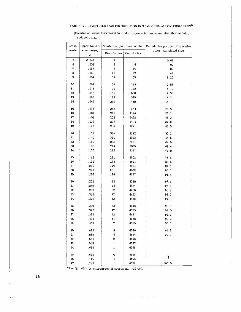
TABLE IV. - PARTICLE SIZE DISTRIBUTION IN TD-NICKEL ALLOY FROM SEEM^
[Counted on Ze i s s Instrument in mode: exponential response, dis t r ibut ive data, r e d u c e d r a n g e . ]
Ze i s s : ount e r
5 6 7 8 9
10 11 12 13 14
15 16 17 18 19
20 21 22 23 24
25 26 27 28 29
30 31 32 33 34
35 36 37 38 39
40 41 42 43 44
45 46 47
Jpper l imi t of s ize range,
Ir
0.049 .053 .056 .060 , 0 6 4
,069 .073 .078 .083 .089
. 094
. l o1 , 1 0 8 ,116 .123
, 1 3 1 .140 , 1 5 0 , 1 6 0 .170
.182 ,194 ,207 . 2 2 1 .236
.252
.269
.287 ,306 .327
.349
.372
.398
.424
.453
.483
.516 , 5 5 1 , 5 8 8 .628
,670 , 7 1 5 . I 6 3
Jumber of par t ic les counted
Distr ibut ive
1 3 6
12 37
59 74
146 181 200
235 240 234 276 287
301 301 268 224 212
211 183 170 201 125
93 74 52 47 32
33 17 12 11 7
5 4 2 1 1
0 0 1
3umulative
1 4
10 22 59
118 192 338 519 719
954 1194 1428 1704 199 1
2292 2593 2861 3085 3297
3508 3691 3861 4062 4187
4280 4354 4406 4453 4485
4518 4535 4547 4558 4565
4570 4574 4576 4577 4578
4578 4578 4579
h m u l a t i v e percent of particle! f iner than stated s ize
0. 02 . 09 . 2 2 . 4 8
1.29
2. 58 4.19 7 . 3 8
1 1 . 3 15 .7
20. 8 2 6 . 1 31.2 37.2 4 3 . 5
50. 1 56.6 62.5 67.4 7 2 . 0
76.6 80 .6 8 4 . 3 8 8 . 7 9 1 . 4
9 3 . 5 9 5 . 1 9 6 . 2 9 7 . 2 9 7 . 9
98.7 99 .0 9 9 . 3 99 .5 99.7
9 9 . 8 99.9
1 100 .0
‘See fig. 4(a) for micrograph of specimen. x12 000.
14
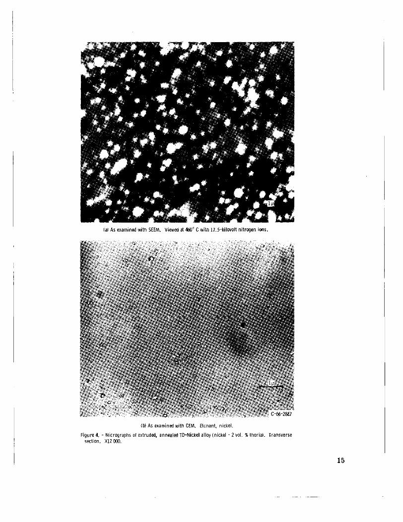
(a) As examined with SEEM. Viewed at 460" C with 17.5-kilovolt nitrogen ions.
(b) As examined with CEM. Etchant, nickel.
Figure 4. - Micrographs of extruded, annealed TD-Nickel alloy (nickel - 2 vol. 70 thoria). Transverse section. X12 000.
15
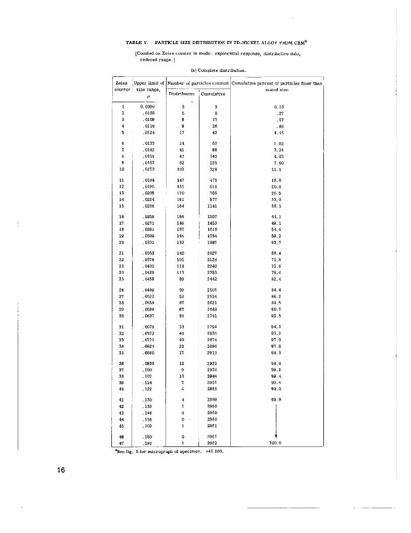
TABLE v. - PARTICLE SIZE DISTRIBUTION IN TD-NICKEL ALLOY FROM C E M ~
[Counted on Zeiss counter in mode: exponential response, distributive data, reduced range.]
(a) Complete distribution.
.0133
.0142 ,0151 .0162 ,0173
Zeiss counter
14 41 47 82
103
size range,
.0353 ,0378 ,0402 ,0429 ,0458
.0489 ,0522 .0558 .0596 .0637
0.0096 ,0102 .0109
4 ,0116 9 26 5 ,0124 17 43
140 101 112 113 89
59 53 67 67 53
6 7 8 9
10
.0678
.0722
.0771 ,0824 .0880
11 12 13 14 15
16 17 18 19 20
53 2794 40 2834 40 2874 22 2896 17 2913
21 22 23 24 25
.0938
. l o o
. lo7
. 114
.122
.130 ,139 ,148 .158 .169
26 27 28 29 30
12 9
10 7 4
4 1 0 0 1
31 32 33 34 35
46 47
36 37 38 39
.160 0 2961
.192 1 2962
I 40 41 42 43 44 45
.OW4
.0196
.0209 ,0224 ,0238
,0256 .0271 .0291 .0309 ,0331
147 131 170 191 164
166 146 157 144 133
57 96
143 225 328
475 616 786 977
1141
1307 1453 1610 1754 1887
2027 2128 2240 2353 2442
2501 2554 2621 2688 2741
2925 2934 2944 2951 2955
2959 2960 2960 2960 2961
Cumulative percent of particles finer than stated size
0.10 .27 .57 .88
1.45
1.92 3.24 4.83 7.60
11.1
16.0 20.8 26.5 33.0 38.5
44.1 49.1 54.4 59.2 63.7
68.4 71.8 75.6 79.4 82.4
84.4 86.2 88.5 90.7 92.5
94.3 95.7 97.0 97.8 98.3
98.8 99.1 99.4 99.6 99.8
99.9
1
100.0
16
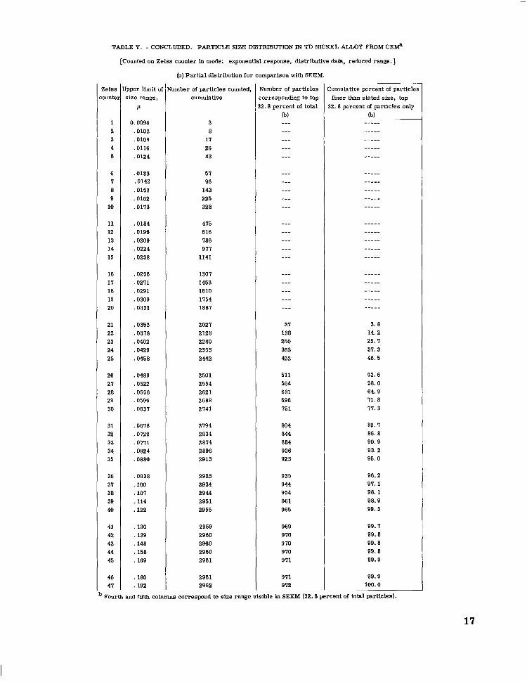
TABLE V. - CONCLUDED. PARTICLE SIZE DISTRIBUTION IN TD NICKEL ALLOY FROM CE+
[Counted on Zeiss counter in mode: exponential response, distributive data, reduced range. ]
(b) Partial distribution for comparison with SEEM.
Zeiss ounte
1 2 3 4 5
6 7 8 9 10
11 12 13 14 15
16 11 18 19 20
21 22 23 24 25
26 21 28 29 30
31 32 33 34 35
36 31 38 39 40
41 42 43 44 45
46 47
rpper limit of s u e range,
!J
0.0096 ,0102 ,0109 ,0116 ,0124
.0133 ,0142 ,0151 .0162 ,0113
,0184 .0196 ,0209 ,0224 ,0238
,0256 .0211 ,0291 ,0309 ,0331
.0353 ,0378 .0402 .0429 ,0458
,0489 .0522 ,0558 ,0596 ,0631
.0618
.0122
.0111 ,0824 .0880
.0938 ,100 ,107 .114 .122
,130 .139 ,148 .158 . 169
,180 .192
lumber of particles counted, cumulative
3 8 17 26 43
57 96 143 225 328
475 616 786 911 1141
1307 1453 1610 1754 1887
2027 2128 2240 2353 2442
2501 2554 2621 2888 2141
2794 2834 2814 2896 2913
2925 2934 2944 2951 2955
2959 2960 2960 2960 2961
2961 2962
Number of particles :orresponding to top #2. 8 percent of total
(b) --- --- -_- --_ ---
37 138 250 363 452
511 564 631 698 751
804 844 884 906 923
935 944 954 961 965
969 910 9 70 970 911
971 9 12
3umulative percent of finer than stated size
32.8 percent of particl
(b) - - -__ ---_- --_-- ---_- - -___
- -___ - -___
3. 8 14.2 25. I 31. 3 46.5
52.6 58.0 64.9 71.8 71.3
82. I 86.8 90.9 93.2 95.0
96.2 97.1 98.1 98.9 99.3
99. 7 99.8 99.8 99.8 99.9
99.9 100.0
Fourth and fifth columns correspond to size range visible in SEEM (32.8 percent of total particles'
17
Part icle Size and Part icle Image Enlargement
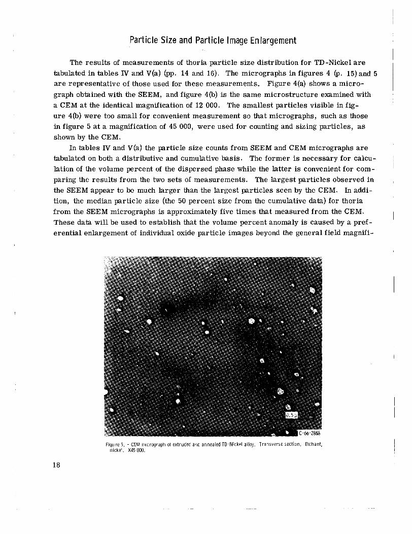
The results of measurements of thoria particle size distribution for TD-Nickel a r e tabulated in tables N and V(a) (pp. 14 and 16). The micrographs in figures 4 (p. 15) and 5 a r e representative of those used for these measurements. Figure 4(a) shows a micro- graph obtained with the SEEM, and figure 4(b) is the same microstructure examined with a CEM at the identical magnification of 12 000. The smallest particles visible in fig- ure 4(b) were too small for convenient measurement so that micrographs, such as those in figure 5 at a magnification of 45 000, were used for counting and sizing particles, as shown by the CEM.
In tables N and V(a) the particle size counts from SEEM and CEM micrographs a r e tabulated on both a distributive and cumulative basis. The former is necessary for calcu- lation of the volume percent of the dispersed phase while the latter is convenient for com- paring the results from the two sets of measurements. The largest particles observed in the SEEM appear to be much larger than the largest particles seen by the CEM. In addi- tion, the median particle size (the 50 percent size from the cumulative data) for thoria from the SEEM micrographs is approximately five times that measured from the CEM. These data will be used to establish that the volume percent anomaly is caused by a pref- erential enlargement of individual oxide particle images beyond the general field magnifi-
Figure 5. - CEM micrograph of extruded and annealed TD-Nickel alloy. Transverse section. Etchant, nickel. X45 000.
18
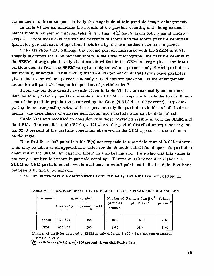
cation and to determine quantitatively the magnitude of this particle image enlargement. In table VI are summarized the results of the particle counting and sizing measure-
ments from a number of micrographs (e. g . , figs. 4(a) and 5) f rom both types of micro- scopes. From these data the volume percents of thoria and the thoria particle densities (particles per unit area of specimen) obtained by the two methods can be compared.
roughly six times the 1.62 percent shown in the CEM micrograph, the particle density in the SEEM micrographs is only about one-third that in the CEM micrographs. The lower particle density from the SEEM can give a higher volume percent only if each particle is individually enlarged. This finding that an enlargement of images from oxide particles gives rise to the volume percent anomaly raised another question: Is the enlargement factor for all particle images independent of particle size?
From the particle density results given in table VI, it can reasonably be assumed that the total particle population visible in the SEEM corresponds to only the top 32.8 per- cent of the particle population observed by the CEM (4.74/14.4XlOO percent). By com- paring the corresponding sets, which represent only the particles visible in both instru- ments, the dependence of enlargement factor upon particle size can be determined.
the CEM. The result is table V(b) (p. 17) where the partial distribution representing the top 32.8 percent of the particle population observed in the CEM appears in the columns on the right.
Note that the cutoff point in table V(b) corresponds to a particle size of 0.035 micron. This may be taken as an approximate value for the detection limit for dispersoid particles observed in the SEEM, at least for thoria in a nickel matrix. Note also that this value is not very sensitive to e r ro r s in particle counting. E r ro r s of *lo percent in either the SEEM or CEM particle counts would still leave a cutoff point and indicated detection limit between 0.03 and 0.04 micron.
The cumulative particle distributions from tables IV and V(b) are both plotted in
The data show that, although the volume percent measured with the SEEM is 9.51,
Table V(a) was modified to consider only those particles visible in both the SEEM and
Instrument
SEEM
CEM
Area counted Number of Particle density, a Volume particles particle/p percent counted
b Micrograph, Specimen field,
124 300 966 4579 4.74 9 .51
415 300 205 2962 14.4 1.62
I ' p 2
2 mm
19
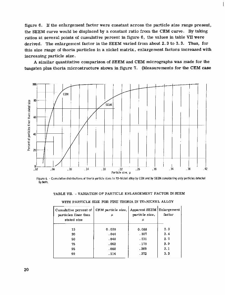
figure 6. If the enlargement factor were constant across the particle size range present, the SEEM curve would be displaced by a constant ratio from the CEM curve. By taking ratios at several points of cumulative percent in figure 6, the values in table VII were derived. The enlargement factor in the SEEM varied from about 2. 3 to 3 .3 . Thus, for this size range of thoria particles in a nickel matrix , enlargement factors increased with increasing particle size.
A similar quantitative comparison of SEEM and CEM micrographs was made for the tungsten plus thoria microstructure shown in figure 7. (Measurements for the CEM case
.02 .06 . I .22 .26 Part icle size, 1.1
T I 1 ..
Figure 6. - Cumulative d is t r ibut ions of thor ia particle sizes in TD-Nickel alloy by CEM and by SEEM considering on ly part icles detected by both.
TABLE VlI. - VARIATION OF PARTICLE ENLARGEMENT FACTOR IN SEEM
WITH PARTICLE SIZE FOR FINE THORIA IN TD-NICKEL ALLOY
particles finer than stated size
I
CEM particle size, I*
0.038 .044 .048 .062 .088 .114
Apparent SEEM particle size,
CL
0.088 .lo7 .131 .178 .269 .372
3 nlarge me nt factor
~
2.3 2.4 2.7 2.9 3.1 3.3
20
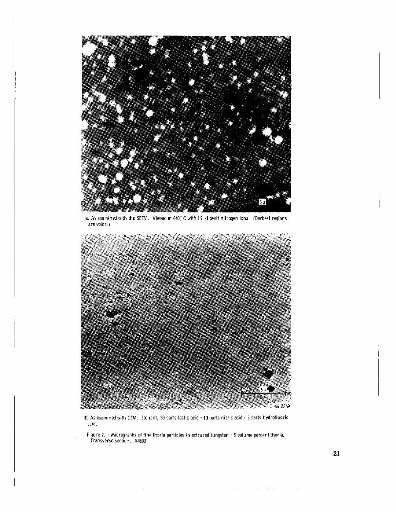
(a) As examined wi th the SEEM. Viewed at 440” C wi th 15-kilovolt nitrogen ions. (Darkest regions are voids.)
(b) As examined wi th CEM. Etchant, 30 parts lactic acid - 10 parts n i t r i c acid - 5 parts hydrofluoric acid.
Figure 7. - Micrographs of f ine thor ia particles in extruded tungsten - 5 volume percent thoria. Transverse section. X4800.
21
were made at X10 000, a higher magnification than that given in figure 7(b).) As is shown in table VIlI, the particle density, as viewed in both instruments, was approximately the same which indicated that all the particles present in this material were above the detec- tion limit of the SEEM. The particle size distributions measured *om the micrographs of figure 7 are tabulated in tables IX and X (pp. 23, 24, and 25). Particle size distribu- tions from both instruments are plotted in figure 8 (p. 26). Table XI (p. 26), which was constructed from figure 8, shows that the enlargement factor for particle images in this tungsten plus thoria material is 2 .3 at a true (CEM) particle size of 0.083 micron but drops to unity at a particle size of about 0.6 micron. This is contrary to the trend in TD -Nickel, where the enlargement factors increased with increasing particle size.
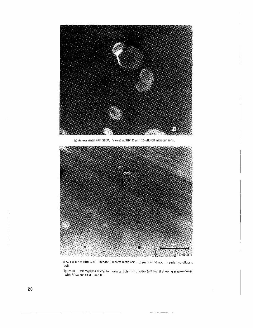
material with coarser thoria particles. The general microstructure of this material is shown in figure 9 (p. 27). By means of a scratch on the specimen and an odd "boomerang- shaped" marker particle, it was possible to locate the identical grouping of particles in both SEEM and CEM micrographs (figs lO(a) and (b) (p. 28), respectively). The diameter of the nearly circular particle image next to the boomerang marker was 4.3 microns when measured by the SEEM and 3.3 microns when measured by a CEM. The enlarge- ment factor here was 1.3.
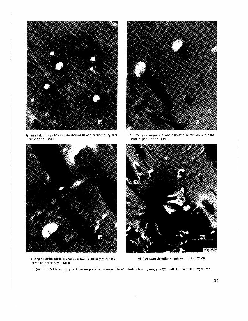
Particle enlargement was also observed but not measured for alumina particles in nickel. In figure 11 (p. 29), which shows shadows cast by the alumina surface particles, the mismatch between image size and width of shadow is taken as evidence of image enlargement, as discussed in the appendix.
Particle enlargement was also measured in another specimen of tungsten-thoria
TABLE VIII. - PARTICLE DENSITY IN TUNGSTEN PLUS 5 VOLUME
PERCENT THORIA AS VIEWED IN SEEM AND C E M ~
Instrument Area counted
(at ~4800)
127 900 (at x10 000)
aSee fig. 7 for micrograph of specimen.
Number of particles counted
1535
1044
Particle density, particle/p 2
0.83
.82
22

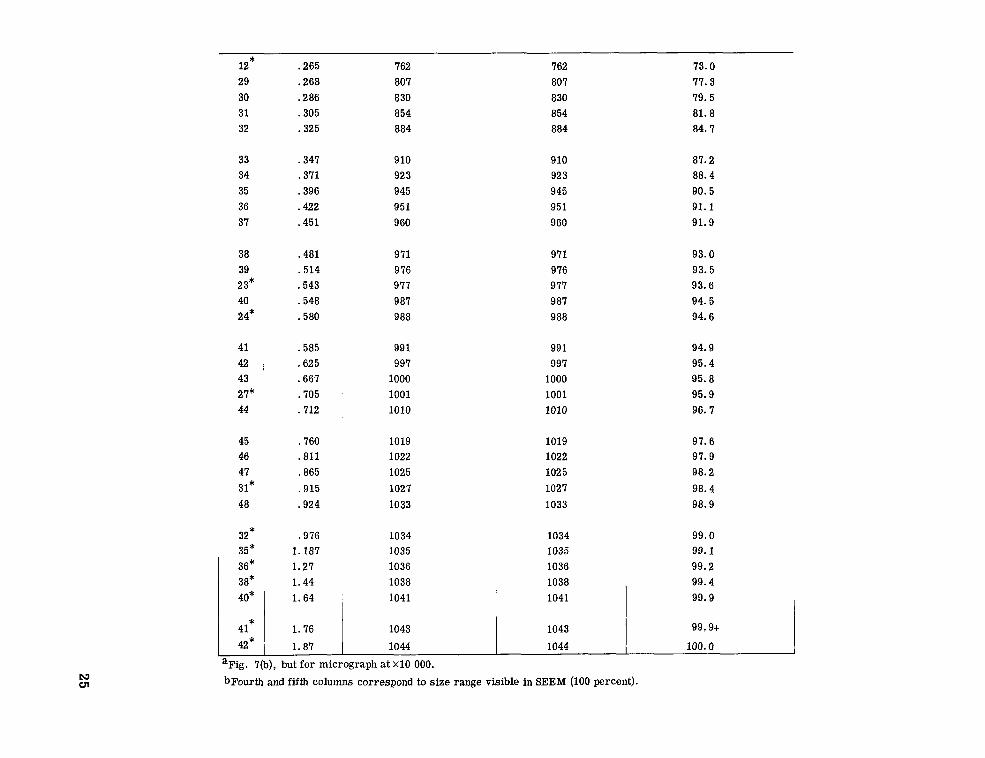
TABLE M. - PARTICLE SIZE DISTRIBUTION IN TUNGSTEN PLUS 5 VOLUME PERCENT
THORIA FROM SEEM. a
[Counted on Zeiss Instrument in mode: exponential response, cumulative data, reduced range. ]
Zeiss ounter
6 7 8 9
10
11 12 13 14 15
16 17 18 19 20
21 22 23 24 25
26 27 28 29 30
31 32 33 34 35
36 37 38 39 40
41 42 43 44 45
46
Jpper limit of s ize range P
0.125 .133 .142 .152 .163
.173
.183
.196
.210
.223
.240
.254
.273
.290
.310
.331
.354
.377
.402
.429
.458
.489
.523
.558
.595
,635 .677 . I 2 3 .772 .825
.879
.939 1.00 1.07 1.14
1.22 1.30 1.39 1.48 1.58
1.69
Jumber of particles counted cumulative
0 3 8
13 --
55 105 163 218 2 82
-__ 431 529 648 777
901 1020 1107 1187 1267
1324 1375 1401 1429 1447
1472 - _ _ _ 1494 1501 1508
1509 1513 1520 1524 1528
1529 1529 1532 1533 1534
1535
__ Cumulative percent of
par t ic les f iner than stated size
0 0.20
.52
.85 _ _ _ _
3.6 6.8 7.6
14.2 18.4
-__- 28.1 34.4 42.2 50.6
58.7 66.4 72.1 77.3 82.5
86.3 89. 6 91.3 93.1 94.3
95.9
97.3 97.8 98.2
98.3 98.6 99.0 99.3 99.5
99.6 99.6 99.8 99.9 99.9
100.0
- -__
aSee fig. 7 for micrograph of specimen. x4800.
23
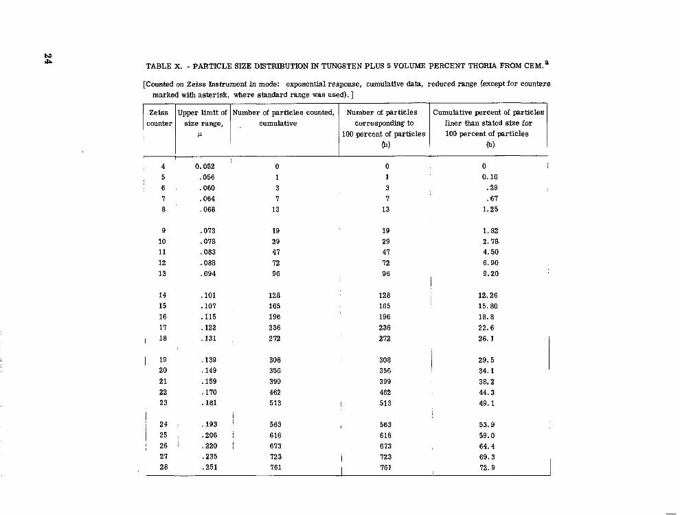
TABLE x. - PARTICLE SIZE DISTRIBUTION IN TUNGSTEN PLUS 5 VOLUME PERCENT THORIA FROM C E M . ~
Zeiss Upper limit of Number of particles counted, Number of particles counter size range, . cumulative corresponding to
!J 100 percent of particles (b)
Cumulative percent of particles finer than stated size for 100 percent of particles
(b)
I 4 0.052 0 0 0 11
5 .056 1 1 0.10 6 .060 3 3 .29 7 .064 7 7 .67 8 ,068 13 13 1.25
9 .073 19 10 .078 29 11 .083 47 12 .088 72 13 .094 96
14 15 16 17
I 18 ,
.lo1
.lo7
.115
.122
.131
128 165 196 236 2 72
19 1.82 29 2.78 47 4.50 72 6.90
I 96 9.20 I 128 12.26 165 I 15.80 196 18.8 236 22.6 272 26.1 ~
12* 29 30 31 32
33 34 35 36 37
38 39 23* 40 24*
41 42 I
43 27* 44
45 46 47 31* 48
32 *
36* 38*
35 *
41*
,265 .268 .286 .305 .325
.347
.371
.396
.422
.451
.481
.514
.543
.548
.580
.585
.625
.667
.705
. 712
.760
.811
.865
.915
.924
.976 1.187 I . 27 1.44 1. 64
1.76
42* 1 1.87
762 807 830 854 884
910 923 945 951 9 60
971 976 977 987 988
991 997
1000 1001 1010
1019 1022 1025 1027 1033
1034 1035 1036 1038 1041 I 1043
1044 I
‘Fig. 7(b), but for micrograph a t X10 000.
762 807 830 854 884
910 92 3 945 951 960
971 9 76 977 987 988
991 997
1000 1001 1010
1019 1022 1025 1027 1033
1034 1035 1036 1038 1041
1043
1044
bFourth and fifth columns correspond to size range visible in SEEM (100 percent).
73.0 77.3 79.5 81.8 84.7
87.2 88.4 90.5 91.1 91.9
93.0 93.5 93.6 94.5 94.6
94.9 95.4 95.8 95.9 96. 7
97.6 97.9 98.2 98.4 98.9
99.0 99.1 99.2 99.4 99.9
99.9+
100.0 I

TABLE XI. - VARIATION OF PARTICLE ENLARGEMENT FACTOR IN SEEM
WITH PARTICLE SIZE FOR FINE THORIA IN TUNGSTEN
Cumulative percent of particles finer than
stated size
5 15 30 50 75 95 99
Single measurement If coarse thoria prticle (fig. 10)
- .
ZEM particle size, !J
0.083 .lo8 .140 .183 .260 .585 .976
3.3
c
Apparent SEEM particle size,
P
0.190 .215 .258 .310 .390 .612
1.000 .-
4.3
.8 1.0 Particle size, p
3 nlar ge me nt factor
2.3 2.0 1.8 1.7 1.5 1.0 1.0
1.3
1. 2 1.4 1.6 1.8
Figure 8. - Cumulative distributions of thoria particle sizes in TD-Nickel alloy by CEM and by SEEM.
26

(a) A s examined wi th SEEM. Viewed at 450" C wi th 17.5-kilovolt nitrogen ions.
(b) A s examined with CEM. Etchant, 30 parts lactic acid - 10 parts n i t r i c acid - 5 parts hydro- f luor ic acid.
Figure 9. - Micrographs of coarse thor ia particles in extruded tungsten - 5 volume percent thoria. Transverse section. X4800.
27
I
(a) As examined wi th SEEM. Viewed at 390" C wi th 15-kilovolt nitrogen ions.
(b) As examined wi th CEM. Etchant, 30 parts lactic acid - 10 parts n i t r i c acid - 5 parts hydrof luor ic acid.
Figure 10. - Micrographs of coarse thor ia particles in tungsten (see fig. 9) showing area examined wi th SEEM and CEM. X4700.
28
(a) Small a lumina particles whose shadows l ie only outside the apparent part icle size. X4800.
(b) Larger a lumina particles whose shadows l ie part ial ly w i th in the apparent part icle size. X4800.
(c) Larger a lumina particles whose shadows l ie part ial ly w i th in the apparent part icle size. X4800.
(d) Persistent distort ion of unknown origin. X1850.
Figure 11. - SEEM micrographs of a lumina particles rest ing on f i l m of colloidal silver. Viewed at 440" C wi th 17.5-kilovolt nitrogen ions.
29
Results of Experiments to Determine Ion Beam Penetration
Additional experiments to solve the volume percent anomaly indicated that the ion beam in the SEEM did not penetrate the surface of a metal specimen to an appreciable depth. The ion beam etching rate was also very low. These results were taken as evi- dence that oxide particles lying below the specimen surface are not imaged.
interference microscope, was vacuum-evaporated onto the TD-Nickel specimen, the thoria dispersion was not visible in the SEEM; only the dark image characteristic of pure nickel was seen. On continuous observation with a low ion beam current, it was noted that the dispersion did not appear gradually in the image; rather the final number and size of thoria particles emerged suddenly when the ion beam had swept away much of the nickel layer.
ion etching rate (surface removal) is high o r that the ion penetration (subsurface illumi- nation) is small. If penetration were substantial, a gradually increasing amount of oxide would be expected in the image because removal of the deposited layer allows an increas- ing depth of the specimen to be illuminated; however, the observed rapid appearance of the oxide image indicates that the ion beam penetration is small.
Another possibility considered was that a rapid ion etching rate, combined with the long photographic exposure times required, might result in micrographs containing images of particles originally below the surface as well as those originally at the surface. If the etching rate by the ion beam were large, the specimen surface would be rapidly swept away. Then, in the 6 to 8 seconds that the shutter to the plate cassette is open in photographically recording the electron image, oxide particles at various depths would become exposed. Since the specimen structure appeared in about 4 minutes under the experimental conditions (0.03 p film of nickel on the surface, examination with 15-kV nitrogen ions at 25-PA beam current), the etching rate of nickel must be on the order of 0.0001 to 0.0002 micron per second (0.03 p/240 sec). The same rate was measured when gold rather than nickel was deposited. With an etching rate of 0.0002 micron per second, the surface of the specimen would be lowered 0.0014 micron during the 7-second exposure required for a typical photograph. This surface lowering represents less than 5 percent of the diameter of an average thoria particle in TD-Nickel (0.03 p ) and so could not account for the observed large increase in a rea fraction of dispersoid.
When a film of approximately 0.03 micron of nickel, as measured with a Zeiss
The sudden appearance of the complete specimen structure implies that either the
Results of Investigation into Irregular Ion Beam Etching
The extent to which irregular ion beam etching might contribute to the volume per-
30
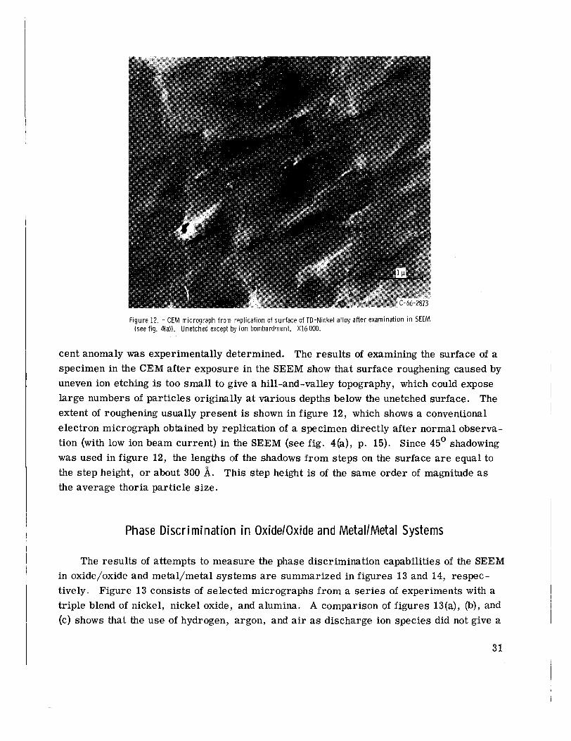
Figure 12. - CEM micrograph from replication of surface of TD-Nickel alloy after examination in SEEM (see fig. 4(a)). Unetched except by i o n bombardment. X16 000.
cent anomaly was experimentally determined. The results of examining the surface of a specimen in the CEM after exposure in the SEEM show that surface roughening caused by uneven ion etching is too small to give a hill-and-valley topography, which could expose large numbers of particles originally at various depths below the unetehed surface. The extent of roughening usually present is shown in figure 12, which shows a conventional electron micrograph obtained by replication of a specimen directly after normal observa- tion (with low ion beam current) in the SEEM (see fig. 4(a), p. 15). Since 45' shadowing was used in figure 12, the lengths of the shadows from steps on the surface a r e equal to the step height, o r about 300 b. This step height is of the same order of magnitude as the average thoria particle size.
Phase Discrimination in Oxideloxide and MetallMetal Systems
The results of attempts to measure the phase discrimination capabilities of the SEEM in oxide/oxide and metal/metal systems are summarized in figures 13 and 14, respec- tively. Figure 13 consists of selected micrographs from a ser ies of experiments with a triple blend of nickel, nickel oxide, and alumina. A comparison of figures 13(a), (b), and (c) shows that the use of hydrogen, argon, and air as discharge ion species did not give a
31

(a) Bombarding ion, hydrogen.
(b) Bombarding ion, argon.
Figure 13. - SEEM photomicrographs of t r ip le blend of nickel - 2.5 volume percent nickel oxide - 2.5 volume percent alumina, dry-blended and explosively compacted. Examined at 445" C wi th various ions at 17.5 kilovolts. X4800.
32
( c ) Bombarding ion, a i r
(d) Bombarding ion, hydrogen.
Figure 13. - Concluded.
33

,-Titanium
,-Zirconium
,- Tan ta I u m
,-Hafnium
,-Tungsten
,-Nickel
/ /
/
/
/ /
/
/
r A l u m i n u m /
/ /
Figure 14. - SEEM photomicrograph of pressed laminate of t i tanium, zirconium, tantalum, hafnium, tungsten, nickel, and a lum inum foils. Viewed at room temperature wi th 17.5-kilovolt nitrogen ions. X670.
clear separation between the two oxide dispersoids. Note that when air was used (fig. 13(c)) the general brightness level of the oxide particle images was higher than that obtained with the other two gases, but there was no apparent difference in brightness levels between the two oxides. The various micrographs in figure 13 a r e presented in the order in which the experiments were performed. Figures 13(a) and (d), both obtained with hydrogen ions, show that the same bombarding ion did not always give the same relative intensities of emission from oxide particles. Similar results (not pictured) were found in experiments where the specimen temperature and the discharge potential were independently varied (see table 111, p. 12). None of the combinations of ion species, discharge potentials, and specimen temperatures used allowed unambiguous discrimina - tion between these two oxides. Two phenomena were observed, which complicated inter- pretation when more than one of the oxide dispersoids was present. Although some oper- ating conditions did produce a variation in particle brightness, the variation appeared as a continuous gradation rather than as distinct steps. An additional problem noted was that the brightness of individual particles alternately increased and decreased with time.
The micrograph of the foil laminate (fig. 14) illustrates the intensity difference between several metals under nitrogen ion bombardment. Note that there appear to be only two general levels of brightness. Zirconium, tantalum, and aluminum a r e much brighter than the other metals. Of interest is the fact that the hafnium foil has an inten- sity gradient. On the left side of the micrograph the intensity closely matches that of the adjacent tungsten foil. On the right side, however, the intensity of hafnium is definitely
34

Figure 15. - SEEM photomicrograph of lamellae of un id i rect ional ly solidified Al-CuA12 eutectic. Viewed at 80" C w i th 15-kilovolt n i t rogen ions. X4700.
intermediate between the two general brightness levels. A secondary emission micrograph of the lamellae of the A1-CuA12 eutectic (fig. 15)
is an additional example of poor phase discrimination by intensity differences in an all- metal system. The image from the as-polished specimen initially showed no phase sepa- ration. Under ion bombardment the aluminum and CuA12 platelets were gradually r e - vealed by preferential ion etching, and their separation was enhanced by using the shal- lowest angle of impingement of the ions. Here the phases are distinguished by their ion- etched topographies rather than by their brightness levels.
Other Practical Examples of Dispersion Microstructures
Viewed by SEEM and by CEM
Micrographs of a number of dispersion alloys of practical interest were taken with both the SEEM and the CEM. The alloys examined included dispersions of thoria and alumina in nickel, alumina in aluminum, thoria in tungsten, and zirconia in a tungsten- tantalum alloy.
cles in TD-Nickel as observed in the SEEM and the CEM, respectively. Thoria particle Nickel-base alloys. - Figures 4(a) and (b) (p. 15) show the dispersion of thoria parti-
35
images are preferentially enlarged in the SEEM as noted in a previous section.
samples. Inspection of such samples can provide useful information for process control in the fabrication of dispersion alloys from powder. Figure 16(a) shows nickel powder with particle sizes of 1 to 2 microns blended with 1 .4 volume percent of a much finer alumina, nominal particle size of 0.02 micron. These powders and proportions were purposely chosen to illustrate poor blending practice. The total surface a rea of the fine alumina was approximately equal to that of the nickel powder. Blending has resulted in an almost continuous network of alumina instead of a dispersion of discrete particles. Note that the alumina network, so clearly visible in the SEEM micrograph in figure 16(a), can hardly be distinguished in the CEM comparison micrograph in figure 16(b).
a blend of 8 volume percent alumina with nickel powder of comparable particle size, both being about 0.02 micron. Although individual particles a r e not resolved, the contrast between phases gives an indication of intimate blending and shows fair uniformity. There a r e some black areas , which can be interpreted as containing few if any alumina particles. Comparison micrographs taken in a CEM are shown in figures 17(b) and (c). The latter has had an annealing treatment to eliminate the matrix roughness, which interferes with observation of particles in figure 17(b).
In the studies of compacted blends of nickel and alumina powders, it was noted that nickel oxide as well as alumina appeared as a bright phase in the SEEM. Figure 13 (pp. 32 and 33) illustrates the inconclusive results of experiments designed to differen- tiate two oxide phases.
Aluminum-base alloys. - A sample of M-257 alloy, aluminum plus 5 weight percent of alumina, was examined in both the SEEM and the CEM. Surprisingly, no bright oxide phase was observed in the polished condition in the SEEM. Subsequently, the specimen was chemically etched, as was done in the preparation for CEM replication, to give the result shown in figure 18(a) (p. 40), where particles a r e visible in relief but not by con- trast. A much clearer distribution was observed in the CEM, as shown in figure 18(b).
Tungsten-base alloys. - Three tungsten-base alloys were examined. Figure 9 (p. 27) shows a dispersion of coarse thoria particles with sizes up to 5 microns in a tungsten matrix. Note the high contrast that can be obtained when particles are well above the resolution limit of the SEEM.
(p. 21). These micrographs were used to determine the dependence of the particle-image enlargement factor on particle size.
powders: a tungsten-zirconium composite and a tantalum powder. The amount of zir- conium present was 0.5 weight percent, and the amount of tantalum, 5 weight percent.
Figures 16 and 17 illustrate the use of the SEEM to examine compacted powder blend
Better blending results are shown in figure 17(a), which is the SEEM micrograph of
A finer dispersion of thoria particles in a tungsten matrix is shown in figure 7
The third tungsten-base alloy examined had been fabricated from a blend of two
36
(a) As examined wi th SEEM. Viewed at 420" C wi th 17.5-kilovolt nitrogen ions.
(b) A s examined wi th CEM. Modified nickel etchant.
Figure 16. - Micrographs of explosively compacted, dryb lended alloy of nickel - 1.4 volume percent alumina. X4800.
37
(a) A s examined wi th SEEM. A s compacted. Viewed at 415" C wi th 17.5-kilovolt nitrogen ions,
(b) A s examined wi th CEM. As compacted, Modified nickel etthant. X6400. Figure 17. - Micrographs of explosively compacted wet-blended alloy of nickel - 8 volume percent
a lumina alloy.
38
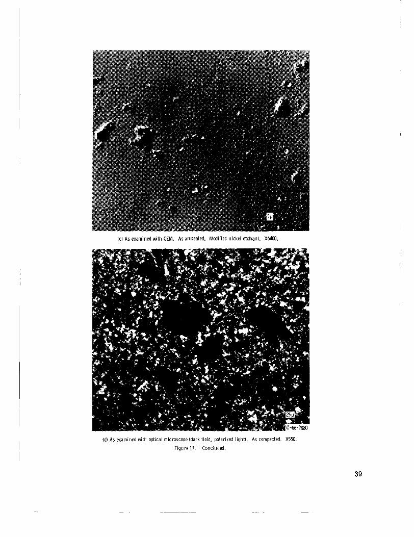
(c) As examined wi th CEM. As annealed. Modified nickel etchant. X6400.
(d) A s examined wi th optical microscope (dark field, polarized light). A s compacted. X550.
Figure 17. - Concluded.
39
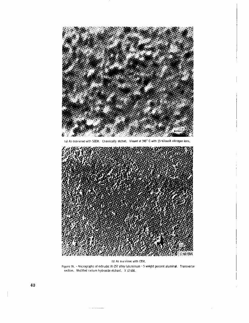
Ib) As examined wi th CEM. Figure 18. - Micrographs of extruded M-257 alloy (a lum inum - 5 weight percent alumina). Transverse
section. Modified sodium hydroxide etchant. X 12 000.
40
(a) As examined wi th SEEM. Chemically etched. Viewed at 390" C with 15-kilovolt n i t rogen ions.

(a) As examined wi th SEEM. Viewed at 410" C wi th 15-kilovolt n i t rogen ions.
(b) A s examined wi th CEM. Etchant, 1 gram sodium hydroxide - 3.5 grams potassium ferr icyanide - 50 mi l l i l i te rs water.
Figure 19. - Micrographs of extruded mult iphase alloy of tungsten - 5 weight percent tanta lum - 0.5 weight percent z i rconium. Longitudinal section. X 12 000. 1
41
Examination of this alloy in the polished condition in the SEEM revealed the mixture of large and small bright spots shown in figure 19(a). On the basis of the relative brightness levels of tungsten and tantalum established in the experiment with the foil laminate (fig. 14, p. 34), the large, bright regions in figure 19(a) were tentatively identified as tantalum-rich areas. Subsequent examination by a CEM using an etchant specific to tantalum (fig. 19(b)) and an electron beam microprobe verified these regions to be in fact tantalum rich. The smaller bright spots in figure 19(a) may be tantalum or zirconia particles.
DISCUSS ION
The usefulness of secondary emission microscopy in the study of dispersion- strengthened metals depends on the extent to which an image of the surface can be ob- tained in which discrete phases can be distinguished and their true size and shape accu- rately measured. This report shows that for the examination of oxides dispersed in metals, great difficulty can be expected in obtaining precise values for microstructural parameters. This section discusses three aspects of the interpretation problem with secondary emission micrographs: resolution, image distortion, and phase discrimina- tion.
Resolution and Detection Limits of SEEM
Although the theoretical resolution limit is about 80 A (ref. 2), the working reso- lution of a secondary emission electron microscope of the type used in this study is generally stated by the manufacturer to be in the range 500 to 1000 A.
During the study of the phenomenon of particle image distortion, it became apparent that dispersion microstructures could be used to obtain an indirect measure of the reso- lution limit of the SEEM. By this indirect measurement, a value of 350 8, which may be called a detection limit, was obtained for TD-Nickel.
That this value is more favorable than the 800-A resolution limit determined in an all-metal system (fig. 3(a), p. 13) is attributed to two factors: the high contrast of the dispersoid-bearing microstructure and the preferential enlargement of the oxide particle images. The detection limit of the SEEM is about one-sixth of the resolution limit ob- tainable in a good light-optical system (2000 A). Conventional electron microscopes, however, commonly have working resolution limits as low as 15 A.
42
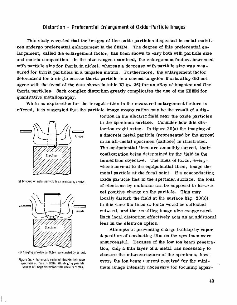
Distortion - Preferential Enlargement of Oxide-Particle Images
This study revealed that the images of fine oxide particles dispersed in metal matri- ces undergo preferential enlargement in the SEEM. The degree of this preferential en- largement, called the enlargement factor, has been shown to vary both with particle size and matrix composition. In the size ranges examined, the enlargement factors increased with particle' size for thoria in nickel, whereas a decrease with particle size was mea- sured for thoria particles in a tungsten matrix. Furthermore, the enlargement factor determined for a single coarse thoria particle in a second tungsten-thoria alloy did not agree with the trend of the data shown in table X I (p. 26) for an alloy of tungsten and fine thoria particles. Such complex distortion greatly complicates the use of the SEEM for quantitative metallography.
While no explanation for the irregularities in the measured enlargement factors is offered, it is suggested that the particle image exaggeration may be the result of a dis-
(a) Imaging of metal particle (represented by arrow).
(b) Imaging of oxide part ic le (represented by arrow).
Figure 20. - Schematic model of e lectr ic f ield near specimen surface in SEEM, i l l us t ra t ing possible source of image distort ion w i th oxide particles.
tortion in the electric field near the oxide particles in the specimen surface. Consider how this dis- tortion might arise. In figure 20(a) the imaging of a discrete metal particle (represented by the arrow) in an all-metal specimen (cathode) is illustrated. The equipotential lines are smoothly curved, their configuration being determined by the field in the immersion objective. The lines of force, every- where normal to the equipotential lines, image the metal particle at the focal point. If a nonconducting oxide particle lies in the specimen surface, the loss of electrons by emission can be supposed to leave a net positive charge on the particle. This may locally disturb the field at the surface (fig. 20(b)). In this case the lines of force would be deflected outward, and the resulting image size exaggerated. Each local distortion effectively acts as an additional lens in the electron optics.
deposition of conducting film on the specimen were unsuccessful. Because of the low ion beam penetra- tion, only a thin layer of a metal was necessary to obscure the microstructure of the specimen; how- ever, the ion beam current required for the mini- mum image intensity necessary for focusing appar-
Attempts at preventing charge buildup by vapor
43
ently removed this conducting layer before observations could be made. The possibility that this problem could be avoided by a particular combination of ion gun species and vapor-deposited film should not be overlooked.
Charging of nonconductors has been observed previously in studies of polycrystalline alumina by secondary emission microscopy (refs. 3 and 9). The distortion appeared first only on certain grains and then in the center of the grain, the grain boundaries remaining undistorted. With time, this charging extended over the whole surface. This effect is surprising, however , with the dilute dispersions of very fine oxide particles where the high surface-to-volume ratio might be expected to allow the charge to be bled off to the conducting matrix.
Phase Discrimination
Three kinds of phase discrimination by the SEEM were examined in this study: dis- crimination between metals and oxides, between oxides and other oxides, and between metals and other metals. The high degree of phase contrast obtained for oxide particles dispersed in metal matrices has been shown in figures 4, 7, 9, and 16. Such high con- trast and uniform intensity across individual particles (e. g. , fig. 9, p. 27) could be ideally adapted to automatic scanning for purposes of quantitative metallography. Unfor - tunately, particle image distortion and the limited resolving power of the SEEM offset the advantage of high contrast.
shows alumina particles in aluminum with minimum dimensions of up to 0.180 micron. The larger particles are well above the detection limit of 0.035 micron determined for the SEEM, and yet they could not be detected by brightness difference alone. Possibly the lack of phase contrast was due to the presence of a film of aluminum oxide over the entire specimen.
,Although the use of the SEEM for precise measurements of dispersion microstruc- tures was found to be greatly hampered by limitations of the instrument, it might be con- sidered as a tool for qualitative examination. For example, the differences between general fineness and uniformity of the dispersions in the compacted powder blends a re readily seen (figs. 16 and 17, pp. 37, 38 and 39). In these cases, however, the SEEM results can be closely approached by light-optical results, although at somewhat lower magnifications. This is shown in figure 17(d), which is a photomicrograph taken with dark-field, polarized light and which corresponds to the SEEM image in figure 17(a).
As was previously pointed out, one of the difficulties in interpreting such dispersion micrographs is the problem of deciding whether all the bright phase observed is in fact the added dispersoid, or whether some of it may represent intrinsic oxide. Experiments
Not all metal/oxide pairs exhibited high-phase contrast, however. Figure 18 (p. 40)
44
with two oxides in nickel indicated that phase discrimination between fine oxide particles in the size range near the resolution limit is unlikely to be achieved in the SEEM.
Brightness levels can often be used to discriminate between certain pairs of metals. With the exception of tantalum, the relative brightness levels of the foils in the foil com- posite of figure 14 (p. 34) were in accord with the relative secondary emission currents given in table I (p. 5). (Emission values for hafnium do not appear in table I. ) The con- trast between bright tantalum and dark tungsten was used to detect tantalum-rich areas in the microstructure shown in figure 19(a) (p. 41). That the areas were in fact rich in tantalum was subsequently confirmed by examination in an electron microprobe.
outside the scope of this study where the various limitations discussed may not preclude successful use of the instrument. Examples of such applications include studies of solid- state phase transformations at elevated temperatures and qualitative aspects of oxidation and reduction phenomena (ref. 1).
It is important to note, however, that there are potential applications of the SEEM
CONCLUSIONS
Various operational aspects of a commercial secondary-emission electron microscope (SEEM) including the working resolution limit and the detection limit were determined. The application of this instrument to the examination of dispersion-strengthened materi- als was investigated. The principal conclusions can be summarized as follows:
1. Secondary-emission microscopy did not appear to be suitable for the quantitative examination of ultrafine oxide dispersions in metal matrices. The advantages of direct examination of an unetched specimen and high matrix/dispersoid contrast were offset by limited resolution and considerable distortion of the images of oxide particles.
in this study was determined to be about 800 A (0.08 p ) ; however, oxide dispersoid particles of true size as small as 350 (0.035 p ) can be detected in the instrument. This more favorable value is believed to result from high matrix/dispersoid contrast and preferential enlargement of oxide images.
as much as three times actual size. This resulted in an abnormally high apparent volume percent of dispersoid. This complex distortion not only precludes direct determination of microstructural parameters, but also apparently rules out simple correction schemes. The distortion is believed to be due to a charging of the nonconducting oxide particles, which magnifies their electron images.
substantially different secondary emission yields. This was true not only for oxide/metal
2. The working resolution limit of the secondary-emission electron microscope used
3. Oxide particles dispersed in metals were imaged with linear dimensions enlarged
4. Useful phase discrimination was evident when phases in the microstructure had
45
composites but was also demonstrated with a laminate of foils of several different metals. An attempt to discriminate between two oxides intermixed in a metal matrix was unsuc- cessful. Under certain conditions the SEEM may reveal phases observable only with great difficulty when conventional etching techniques are employed. Such phases are distinguished either by their different secondary electron emission characteristics or by a topographic separation resulting from their different rates of ion etching.
Lewis Research Center, National Aeronautics and Space Administration,
Cleveland, Ohio, July 14, 1966, 129-03-01 -05-22.
I’
46
APPENDIX - QUALITATIVE RllDENCE FOR IMAGE DISTORTION
The quantitative results are supported by qualitative evidence for an exaggeration of the oxide particle size when viewed in the SEEM. In all the micrographs obtained in this study, the images from oxide particles were not sharp. Although the metal matrix was often etched into sharply defined contours, the oxide particles appeared without any topo- graphic detail. If the particles were imaged accurately, irregular oxide/matrix inter- faces as observed in conventional electron microscopy would be visible (especially with the largest particles).
Additional insight into the distortion phenomenon came from observing the shadows of particles lying on the surface of the specimens. With insufficient washing of the pol- ished specimen before examination or after a high-voltage discharge in the microscope during a run, oxide particles appeared resting on the surface. The shadows from these particles were invariably smaller than the particle image. The ratio of maximum shadow diameter to apparent particle diameter varied widely in a given specimen, which pro- vided further evidence for a variable enlargement factor. Figures l l (a ) to (c) (p. 29) illustrate the two types of shadows that were observed. With small alumina particles, shadows such as those in figures ll(a) and (b) were seen. The diameter of the shadow at its base is assumed to be approximately the true diameter of the particle. The length and shape of the shadow indicate the height and shape of the particle. With larger parti- cles (fig. l l(c)) , the shadow extends into the apparent particle area. This can be ex- plained by assuming that the ion beam did not completely penetrate the particle and that no emission therefore occurred on the dark side. With smaller particles there is suffi- cient emission from the whole surface to restrict the shadow to the region outside the apparent area of the particle. Figure l l (d) is an example of a persistent distortion that appears occasionally in SEEM micrographs. It is not clear what causes this effect.
47
REFERENCES
1. Watts, R. D. : Surface Electron Microscopy. Metallurgia, vol. 66, no. 394, Aug. 1962, pp. 98-102.
2. Moellenstedt, G. : and Lenz, F. : Electron Emission Microscopy. Vol. 18 of Advances in Electronics and Electron Physics, L. Marton, ed. , Academic Press, hc., 1963, pp. 251-329.
3. Thornley, R. F. M. ; and Cartz, L. : Direct Examination of Ceramic Surfaces with the Scanning Electron Microscope. Am. Ceramic SOC. J. , vol. 45, no. 9, Sept. 1962, pp. 425-428.
4. Bruining, H. : Physics and Applications of Secondary Electron Emission. Pergamon Press, 1954.
5. Kaminsky, Manfred: Atomic and Ionic Impact Phenomena on Metal Surfaces. Academic Press, 1965.
6. Gaukler, Karl H. : Messung der Elektronen-Emission im Metalloberfkkhenmikroskop. Z. Metallk., vol. 51, 1960, pp. 463-466.
7. Reinhardt, Gustav; Cremens, Walter S. ; and Weeton, John W. : Cold Consolidation of Metal plus Dispersoid Blends for Examination by Electron Microscopy. NASA TN D-3511, 1966.
8. Endter, F. ; and Gebauer, H. : Ein einfaches Gerat zur statistischen Auswertung von microskopischen bzw. elektronenmikroskopischen Aufnahmen. Optik, vol. 13, no. 3, 1956, pp. 97-101.
9. Cartz, L. ; Moellenstedt, G. ; and Septier, A. : Emission Electron Microscope Studies of Ceramic Materials. Transactions of the VIIIth International Ceramic Congress, Copenhagen, 1962, pp. 21-28.
48 NASA-Langley, 1966 E-3471
“The aeronautical and space activities of the United States shall be conducted so as to contribute . . . to the expansion of hzrman KnowI-
The Administration vhall provide for the widest practicable and appropriate dissemination of information concernitig its activities and the results thereof .”
%; edge of phenomena in the atmosphere and space.
-NATIONAL AERONAUTICS AND SPACE ACT OF 1958
NASA SCIENTIFIC AND TECHNICAL PUBLICATIONS
TECHNICAL REPORTS: important, complete, and a lasting contribution to existing knowledge.
TECHNICAL NOTES: of importance as a contribution to existing knowledge.
TECHNICAL MEMORANDUMS: Information receiving limited distri- bution because of preliminary data, security classification, or other reasons.
CONTRACTOR REPORTS: Technical information generated in con- nection with a NASA contract or grant and released under NASA auspices.
TECHNICAL TRANSLATIONS: Information published in a foreign language considered to merit NASA distribution in English.
TECHNICAL REPRINTS: Information derived from NASA activities and initially published in the form of journal articles.
SPECIAL PUBLICATIONS: Information derived from or of value to NASA activities but not necessarily reporting the results .of individual NASA-programmed scientific efforts. Publications include conference proceedings, monographs, data compilations, handbooks, sourcebooks, and special bibliographies.
Scientific and technical information considered
Information less broad in scope but nevertheless
Details on the availability o f these publications may be obtained from:
SCIENTIFIC AND TECHNICAL INFORMATION DIVISION
NATIONAL AERONAUTICS AND SPACE ADMl NlSTRATlO N
Washington, D.C. PO546