Embed Size (px)
Citation preview
Fault Tolerant Hierarchical Control Strategy for
Modular Multilevel Converter in HVDC Application
Paul Dan Burlacu
Master Thesis
Power Electronics and Drives
Department of Energy Technology, Aalborg University

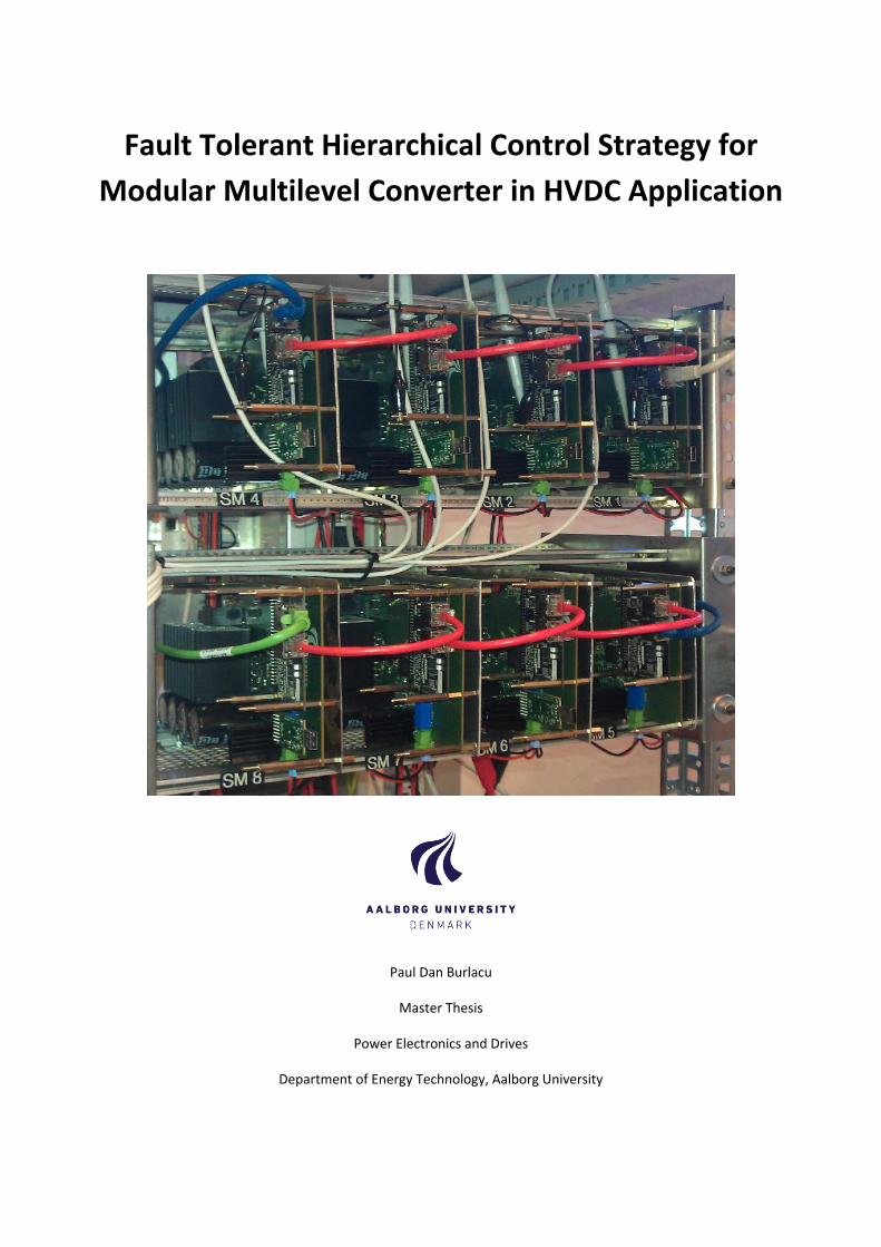
Title: [Fault Tolerant Hierarchical Control Strategy for Modular Multilevel Converter in HVDC
Application]
Semester: [9/10]
Semester theme: [Master Thesis]
Project period: [01/09/2013 – 26/6/2014]
ECTS: [50]
Supervisor: [Remus Teodorescu and Laszlo Mathe]
Project group: [PED4 - 1044]
_____________________________________
[Paul Dan Burlacu]
Copies: [3]
Pages, total: [95]
Appendix: [1]
Supplements: [1 CD]
By signing this document, each member of the group confirms that all group members have
participated in the project work, and thereby all members are collectively liable for the
contents of the report. Furthermore, all group members confirm that the report does not
include plagiarism.
SYNOPSIS:
The Modular Multilevel Converter (MMC) has
proven itself to be a good solution for High Voltage
Direct Current Applications due to its high
modularity, scalability and low output voltage
harmonic distortion.
One the main challenges of the MMC is the control. It
is known that commercially available solutions use a
centralized control topology, where a single controller
is used to perform all the necessary calculations and
processing of the MMC control.
The aim of this thesis is to develop a control strategy
using the hierarchical control topology approach.
Using EtherCAT communication network a method
for synchronizing the carrier waves of the MMC is
developed and the resampled phase shifted PWM
algorithm is implemented for different configurations
of the MMC.
In order to improve the reliability of the system an
algorithm is developed to reconfigure the system in
case of a fault in one of the MMC sub-modules. The
averaging and balancing control of the MMC is
studied through simulations.

Preface
The ‘Fault Tolerant Hierarchical Control Strategy for Modular Multilevel Converter in HVDC
Application’ master thesis was conducted at the Department of Energy Technology, Aalborg University,
between the 1st of September 2013 and 26th of May 2014 as the final part of the study curriculum
requirements for graduation of the two year Master program Power Electronics and Drives.
The thesis was followed by the supervisors Professor Remus Teodorescu and Associate Professor
Laszlo Mathe. I truly thank them both for their great support and supervision throughout the entire project
period.
I would also like to thank Emanuel-Petre Eni for his support and introduction to EtherCAT
communication protocol, Lorand Bede for his help regarding the CPLD programming, Marcos Rejas for
helping me with the hardware solder and Heverton Pereira for his support in the laboratory.
25 - 5 - 2014
Paul Dan Burlacu

Summary
The present work is divided in six main chapters and one appendix.
In chapter number one a small introduction to the modular multilevel converter (MMC) technology
for high voltage direct current is made. The evolution of the different converter types until the MMC is
given starting with line commutated converters. Problem formulation, problem objectives and project
limitations are also presented in this chapter.
In the second chapter the one phase MMC with eight half-bridge sub-modules is explained. The
phase shifted – PWM technique is explained and analyzed. The equations which model the behavior of the
MMC are derived and a small introduction to the different control topologies for MMC is given. At the end
of the chapter EtherCAT communication protocol and some of its feature are introduced.
The third chapter covers two of the main aspects developed throughout the project. The first aspect
is the development of a method to synchronize the carrier waves of the sub-modules controllers using
EtherCAT Distributed Clocks mechanism. The second aspect is the development of the resampled phase
shifted PWM algorithm for different MMC configurations employing 4, 6 and 8 sub-modules.
The fourth chapter of the project explains the philosophy of the system by means of different state
machine diagrams.
The fifth chapter covers the inner control of the MMC. The averaging capacitor voltage control and
individual balancing control are explained and simulation results are presented. At the end of the chapter
measurement of the upper and lower voltage waveforms using 3 and 4 sub-modules per arm are shown.
In the appendix a copy of the paper based on the work carried out during this project which was
published in 2014 OPTIM conference is attached.

Contents
Chapter 1: Introduction ....................................................................................................................................................... 1
1.1. High Voltage Direct Current. ............................................................................................................................ 1
1.2. Line Commutated Converters and Voltage Source Converters HVDC Technologies. ..................................... 2
1.3. Voltage Source Converter topologies for HVDC application. .......................................................................... 2
1.4. State of the art of MMC and project motivation. .............................................................................................. 3
1.5. Project formulation. ........................................................................................................................................... 5
1.6. Project objectives. ............................................................................................................................................. 5
1.7. Project limitations. ............................................................................................................................................ 6
Chapter 2: Introduction to the modular multilevel converter .............................................................................................. 7
2.1. MMC elements description. .............................................................................................................................. 7
2.2. MMC sub-module elements description. .......................................................................................................... 8
2.3. Phase shifted PWM and MMC operation principle. .......................................................................................... 9
2.3.1. Single sub-module analysis. .......................................................................................................................... 9
2.3.2. Upper arm series connected sub-modules analysis with no phase shift between the carrier waves. ........... 11
2.3.3. Upper arm series connected sub-modules analysis with phase shift between the carrier waves................. 12
2.3.4. Upper and lower arm series connected sub-modules analysis with phase shift between the carrier waves.14
2.4. MMC fundamental equations. ......................................................................................................................... 15
2.5. MMC control topologies. ................................................................................................................................ 16
2.6. EtherCAT. ....................................................................................................................................................... 18
2.6.1. Basic operation principle. ........................................................................................................................... 18
2.6.2. Distributed Clocks. ..................................................................................................................................... 18
2.6.3. Galvanic isolation. ...................................................................................................................................... 19
2.6.4. Integration of EtherCAT in the MMC design ............................................................................................. 19
Chapter 3: Resampled phase shifted PWM ...................................................................................................................... 21
3.1. Resampled phase shifted PWM for MMC. ..................................................................................................... 21
3.1.1. Sub-module counters synchronization. ....................................................................................................... 21
3.1.2. Resampled Phase Shifted PWM Carrier signal implementation. ................................................................ 23
3.2. Resampled PWM for MMC with 4 sub-modules. ........................................................................................... 28
3.2.1. Measured and simulated resampled PS PWM signals at 1.1818 kHz switching frequency. ....................... 30
3.3. Resampled PWM for MMC with 6 sub-modules. ........................................................................................... 31
3.3.1. Measured and simulated resampled PS PWM signals at 1kHz switching frequency.................................. 34
3.4. Resampled PWM for MMC with 8 sub-modules. ........................................................................................... 35
3.4.1. Measured and simulated resampled PS PWM signals at 1.1818kHz switching frequency. ........................ 38
Chapter 4: Description of the MMC system ..................................................................................................................... 39
4.1. Operator of the system. ................................................................................................................................... 39
4.2. Central Controller. ........................................................................................................................................... 40
4.3. Central controller state machine. ..................................................................................................................... 44
4.4. Sub-module local controller. ........................................................................................................................... 49
4.5. Sub - module controller state machine. ........................................................................................................... 51
Chapter 5: Control of the MMC ....................................................................................................................................... 57
5.1. MMC capacitor voltage unbalancing. ............................................................................................................. 57
5.2. Capacitor Voltage Averaging Control ............................................................................................................. 58
5.3. Individual capacitor voltage balancing control. .............................................................................................. 58
5.4. Simulation results 8 sub-module MMC. ......................................................................................................... 59
5.5. Simulation results 6 sub-module MMC. ......................................................................................................... 63
5.6. Measured results .............................................................................................................................................. 67
Chapter 6: Conclusions and future work .......................................................................................................................... 73
6.1. Conclusions ......................................................................................................................................................... 73
5.7. Future work. .................................................................................................................................................... 73
References ........................................................................................................................................................................ 75
Appendix A : OPTIM Conference 2014 Paper ................................................................................................................. 77
1
Chapter 1: Introduction
1.1. High Voltage Direct Current.
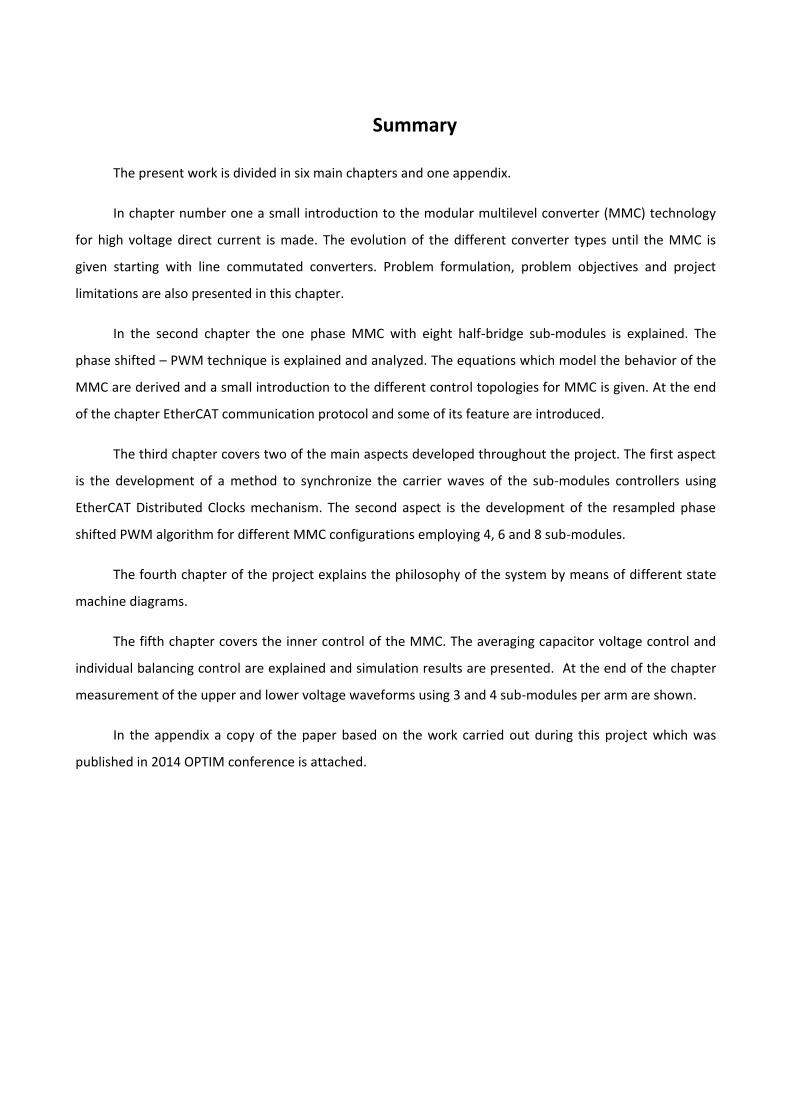
High Voltage Direct Current (HVDC) is, along with High-Voltage-Alternating-Current (HVAC), one of the two
technologies used for electric power transmission over long distances. When transmission distances of several
hundreds of kilometers are exceeded, the pertinent viability study is executed in order to decide between the HVDC
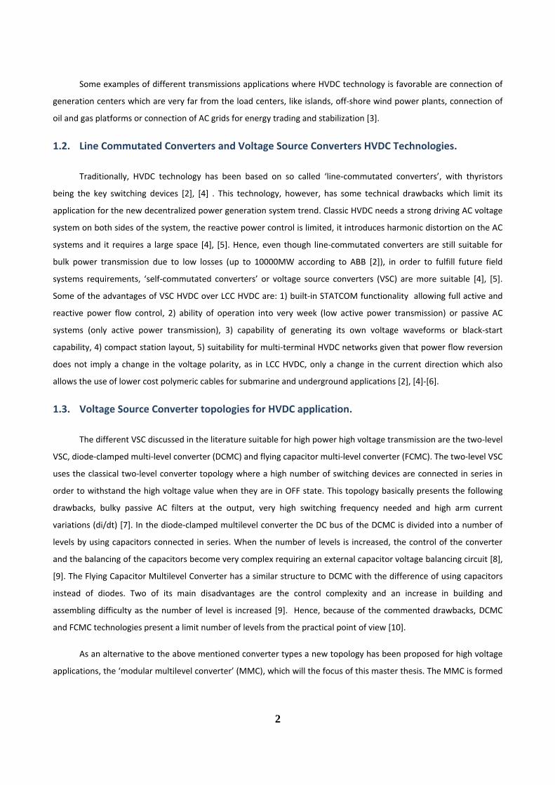
or HVAC implementation. In Figure 1 a typical cost comparison curve between the two technologies is shown taking
into account station terminal costs, line costs and losses costs [1].
DC Losses
AC Losses
Total AC CostTotal DC Cost
DC Line
DC Terminals
AC Line
AC Terminals
Break-EvenDistance
Transmission Distance
Costs
Figure 1. Typical HVDC and HVAC costs comparison curve [1].
The usage of HVDC starts being economically attractive when the break-even distance is exceeded. The reason
for this is that the capacitive and inductive losses associated with AC links become very large and the total costs are
higher than those of HVDC technology. This translates into more transmission lines needed and more land coverage
for AC systems. The break-even distance lays somewhere between 500 and 800km [1]. For underwater cables, this
range decreases to values between 50-100km, depending on the grid conditions and transmitted power. The main
advantages of HVDC technology over HVAC in long transmission distances are 1) lower costs due to lower losses, 2) no
cable length limit, 3) possibility of underground cables usage, 4) allows connections of asynchronous grids, 5) static
magnetic fields which no cause electromagnetic interference and 6) no need of intermediate stations [2].
2
Some examples of different transmissions applications where HVDC technology is favorable are connection of
generation centers which are very far from the load centers, like islands, off-shore wind power plants, connection of
oil and gas platforms or connection of AC grids for energy trading and stabilization [3].
1.2. Line Commutated Converters and Voltage Source Converters HVDC Technologies.
Traditionally, HVDC technology has been based on so called ‘line-commutated converters’, with thyristors
being the key switching devices [2], [4] . This technology, however, has some technical drawbacks which limit its
application for the new decentralized power generation system trend. Classic HVDC needs a strong driving AC voltage
system on both sides of the system, the reactive power control is limited, it introduces harmonic distortion on the AC
systems and it requires a large space [4], [5]. Hence, even though line-commutated converters are still suitable for
bulk power transmission due to low losses (up to 10000MW according to ABB [2]), in order to fulfill future field
systems requirements, ‘self-commutated converters’ or voltage source converters (VSC) are more suitable [4], [5].
Some of the advantages of VSC HVDC over LCC HVDC are: 1) built-in STATCOM functionality allowing full active and
reactive power flow control, 2) ability of operation into very week (low active power transmission) or passive AC
systems (only active power transmission), 3) capability of generating its own voltage waveforms or black-start
capability, 4) compact station layout, 5) suitability for multi-terminal HVDC networks given that power flow reversion
does not imply a change in the voltage polarity, as in LCC HVDC, only a change in the current direction which also
allows the use of lower cost polymeric cables for submarine and underground applications [2], [4]-[6].
1.3. Voltage Source Converter topologies for HVDC application.
The different VSC discussed in the literature suitable for high power high voltage transmission are the two-level
VSC, diode-clamped multi-level converter (DCMC) and flying capacitor multi-level converter (FCMC). The two-level VSC
uses the classical two-level converter topology where a high number of switching devices are connected in series in
order to withstand the high voltage value when they are in OFF state. This topology basically presents the following
drawbacks, bulky passive AC filters at the output, very high switching frequency needed and high arm current
variations (di/dt) [7]. In the diode-clamped multilevel converter the DC bus of the DCMC is divided into a number of
levels by using capacitors connected in series. When the number of levels is increased, the control of the converter
and the balancing of the capacitors become very complex requiring an external capacitor voltage balancing circuit [8],
[9]. The Flying Capacitor Multilevel Converter has a similar structure to DCMC with the difference of using capacitors
instead of diodes. Two of its main disadvantages are the control complexity and an increase in building and
assembling difficulty as the number of level is increased [9]. Hence, because of the commented drawbacks, DCMC
and FCMC technologies present a limit number of levels from the practical point of view [10].
As an alternative to the above mentioned converter types a new topology has been proposed for high voltage
applications, the ‘modular multilevel converter’ (MMC), which will the focus of this master thesis. The MMC is formed
3
by a number of sub-modules connected in series, which have exactly the same hardware configuration. The MMC has
proved to be superior to its competitors for HVDC applications presenting the following main advantages [10]:
hundreds of voltage levels can be achieved
easier voltage balancing control
no series-connected semiconductor switches
high modularity
easily scalability to different power and voltage levels
low total harmonic distortion and low switching frequencies which translates in small filters and low
switching losses
Although different MMC sub-module topologies for HVDC can be found in the literature, as ‘clamped-doubled
sub-module’, ‘five level cross connected sub-module’ or the ‘current source inductor’ sub-module, the most common
topologies are the ‘half bridge’ and ‘full-bridge’ sub-modules. Generally speaking, both full-bridge and half bridge
MMC offer similar performances for active and reactive power control in normal operation as well as transients.
However, even though the full bridge configuration is able to block the fault current during a DC short-circuit fault, it
utilizes the double of switching components which translates into higher switching losses and hence, an increase of
the converter costs [11]-[13]. This project is based on MMC with half-bridge sub-module configuration.
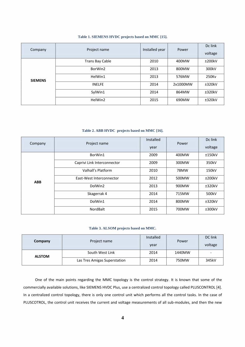
1.4. State of the art of MMC and project motivation.
High Voltage Direct Current systems based on half bridge MMC topology have become a commercially available
solution offered by different companies in the recent years under names like HVDC PLUS of SIEMENS and HVDC Light
of ABB. In the case of ALSTOM, even though they also have a prototype based on half-bridge MMC, they will use
hybrid topologies in the future [5], [14]. Some examples of real MMC based HVDC systems are given in Table 1, Table
2 and Table 3.
4
Table 1. SIEMENS HVDC projects based on MMC [15].
Company Project name Installed year Power Dc link
voltage
SIEMENS
Trans Bay Cable 2010 400MW ±200kV
BorWin2 2013 800MW 300kV
HelWin1 2013 576MW 250Kv
INELFE 2014 2x1000MW ±320kV
SylWin1 2014 864MW ±320kV
HelWin2 2015 690MW ±320kV
Table 2. ABB HVDC projects based on MMC [16].
Company Project name Installed
year Power
Dc link
voltage
ABB
BorWin1 2009 400MW ±150kV
Caprivi Link Interconnector 2009 300MW 350kV
Valhall’s Platform 2010 78MW 150kV
East-West Interconnector 2012 500MW ±200kV
DolWin2 2013 900MW ±320kV
Skagerrak 4 2014 715MW 500kV
DolWin1 2014 800MW ±320kV
NordBalt 2015 700MW ±300kV
Table 3. ALSOM projects based on MMC.
Company Project name Installed
year Power
DC link
voltage
ALSTOM South West Link 2014 1440MW -
Las Tres Amigas Superstation 2014 750MW 345kV
One of the main points regarding the MMC topology is the control strategy. It is known that some of the
commercially available solutions, like SIEMENS HVDC Plus, use a centralized control topology called PLUSCONTROL [4].
In a centralized control topology, there is only one control unit which performs all the control tasks. In the case of
PLUSCOTROL, the control unit receives the current and voltage measurements of all sub-modules, and then the new
5
references for the output and capacitors voltage control is performed at times intervals of a few microseconds [4]. The
requirements of the centralized control topology are the following:
Very high communication bandwidth given that hundreds of measurements need to be performed
Very high processing speed of the controller because hundreds of new switching states need to be
calculated in a very limited time of several microseconds
1.5. Project formulation.
The control of the MMC is not an easy task and it is known that a centralized control topology has been
successfully adopted for commercially available HVDC based on MMC products like SIEMENS HVDC PLUS. Besides this,
a different control topology has been proposed and needs further study and investigation; this is the hierarchical
control topology. The aims of this topology are:
To reduce the required processing speed by adding more processors to the system and distributing
the different control task between them. In addition to the main controller of the centralized control
topology each sub-module of the MMC will have its controller. The main or central controller will
perform the high level control tasks and the sub-modules processors the low level control tasks.
To reduce the required communication bandwidth. As the control tasks are split between the different
controllers, less data needs to be sent to the central controller.
1.6. Project objectives.
The main objective of the current project is to develop a new hierarchical control strategy based on EtherCAT
communication protocol. In order to achieve this, the following objectives need to be fulfilled:
Synchronization of the carrier signals of all the MMC sub-modules.
Implementation of Phase Shifted PWM based on resampled technique.
Implementation of system reconfiguration technique in case of communication or electric fault.
Implementation of arm voltage ‘averaging’ control.
Implementation of individual capacitor voltage balancing control.
Implementation of output current control.
6
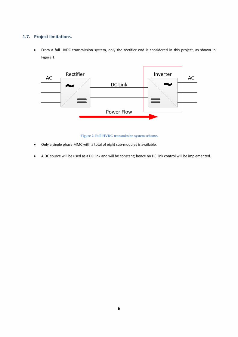
1.7. Project limitations.
From a full HVDC transmission system, only the rectifier end is considered in this project, as shown in
Figure 1.
DC Link
Rectifier Inverter
Power Flow
AC AC
Figure 2. Full HVDC transmission system scheme.
Only a single phase MMC with a total of eight sub-modules is available.
A DC source will be used as a DC link and will be constant; hence no DC link control will be implemented.
7
Chapter 2: Introduction to the modular multilevel converter
In this chapter a description of the modular multilevel converter is given. Its functionality is explained starting
with a general description of the elements of the MMC. Afterwards, the phase shifted PWM technique is also
explained starting from the most basic element of the MMC, a single sub-module, and adding different sub-modules
until the full design is obtained. All the descriptions given are focused only on the single phase MMC with a total of 8
sub-modules. The MMC is considered to be working only as an inverter; hence the power flow will always be
considered from the DC side to the AC side. A description of the suitable control topologies for MMC and EtherCAT
communication protocol are also given.
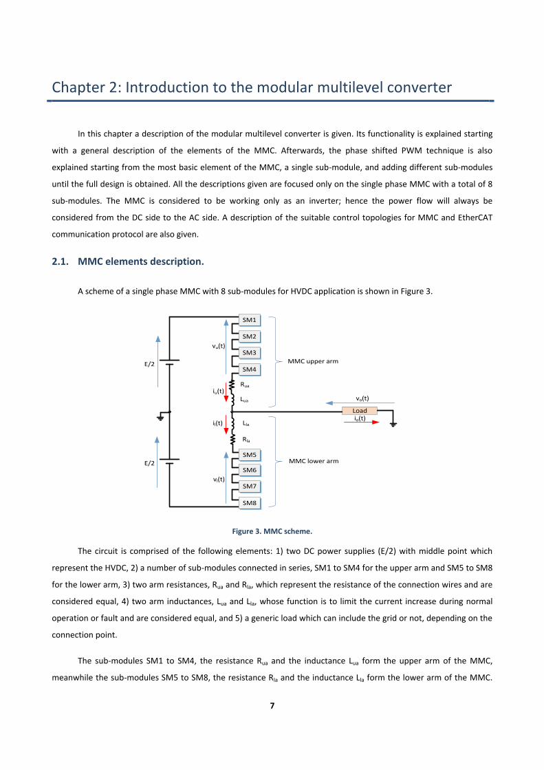
2.1. MMC elements description.
A scheme of a single phase MMC with 8 sub-modules for HVDC application is shown in Figure 3.
E/2
Lla
Lua
SM1
SM3
SM4
SM2
SM7
SM8
SM6
SM5E/2
Rla
Rua
Load
vu(t)
iu(t)
il(t)
vl(t)
io(t)
vo(t)
MMC upper arm
MMC lower arm
Figure 3. MMC scheme.
The circuit is comprised of the following elements: 1) two DC power supplies (E/2) with middle point which
represent the HVDC, 2) a number of sub-modules connected in series, SM1 to SM4 for the upper arm and SM5 to SM8
for the lower arm, 3) two arm resistances, Rua and Rla, which represent the resistance of the connection wires and are
considered equal, 4) two arm inductances, Lua and Lla, whose function is to limit the current increase during normal
operation or fault and are considered equal, and 5) a generic load which can include the grid or not, depending on the
connection point.
The sub-modules SM1 to SM4, the resistance Rua and the inductance Lua form the upper arm of the MMC,
meanwhile the sub-modules SM5 to SM8, the resistance Rla and the inductance Lla form the lower arm of the MMC.
8
The voltages vu(t) and vl(t) represent the voltages at the series-connected sub-modules terminals in the upper and
lower arm respectively. iu(t) and il(t) are the currents in the upper and lower arm. vo(t) and io(t) are the output voltage
and current of the MMC. The number of levels of the output voltage depends on the number of sub-modules and is
given by N+1, where N represents the total number of sub-modules in the MMC. Hence, if the total number of sub-
modules is 8, the output voltage will have 9 levels, as shown in the following sections.
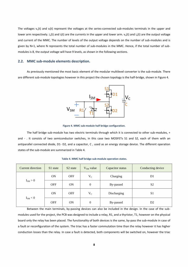
2.2. MMC sub-module elements description.
As previously mentioned the most basic element of the modular multilevel converter is the sub-module. There
are different sub-module topologies however in this project the chosen topology is the half-bridge, shown in Figure 4.
S1
S2
VC
VSM
C
D1
D2R1T1
ISM
Figure 4. MMC sub-module half bridge configuration.
The half bridge sub-module has two electric terminals through which it is connected to other sub-modules, +
and - . It consists of two semiconductor switches, in this case two MOSFETs S1 and S2, each of them with an
antiparallel connected diode, D1- D2, and a capacitor, C , used as an energy storage device. The different operation
states of the sub-module are summarized in Table 4.
Table 4. MMC half bridge sub-module operation states.
Current direction S1 state S2 state VSM value Capacitor status Conducting device
ISM > 0
ON OFF VC Charging D1
OFF ON 0 By-passed S2
ISM < 0
ON OFF VC Discharging S1
OFF ON 0 By-passed D2
Between the main terminals, by-passing devices can also be included in the design. In the case of the sub-
modules used for the project, the PCB was designed to include a relay, R1, and a thyristor, T1, however on the physical
board only the relay has been placed. The functionality of both devices is the same, by-pass the sub-module in case of
a fault or reconfiguration of the system. The triac has a faster commutation time than the relay however it has higher
conduction losses than the relay. In case a fault is detected, both components will be switched on, however the triac
9
will conduct only at the beginning until the relay is closed, then it will be turned off and only the relay will be
conducting.
In order to obtain a correct operation mode, the voltage in the capacitor must be kept to a relatively constant
value of Vc = 2E / N. For the present project, the voltage E has a value of 400V and N is equal to 8, hence the capacitor
voltage must be kept close to 100V. This is achieved through the capacitor voltage averaging control and capacitor
voltage balancing control which will be discussed in the following chapters.
2.3. Phase shifted PWM and MMC operation principle.
Different PWM techniques can be found in the literature for MMC. Some of these techniques, known as multi-
carrier PWM techniques, are based on comparing a sinusoidal reference signal with a triangular carrier signal. The
best known multi-carrier PWM techniques are Phase Disposition (PD), Phase Opposition Disposition (POD), Alternative
Phase Opposition Disposition (APOD) and Phase Shifted PWM technique (PS) [17], [18]. In this project Phase Shifted
PWM technique is used for the lower harmonic content generated at the output voltage and its easy usage for
hierarchical control [17] and because it presents the best natural performance for the capacitor voltage balancing of
the sub-modules [19], [20].
2.3.1. Single sub-module analysis.
In order to understand the operation principle of the MMC and the phase shifted PWM technique, a single half-
bridge sub-module as the one from Figure 4 is considered in first place. Considering that there is no current flowing
through the sub-module and that the capacitor voltage is kept at its nominal value, Vc = 100V, a general analysis of the
voltage waveform at the sub-module terminals is shown below by applying the classical PWM modulation technique.
Different figures showing the different wave forms are given below. The reference signal is a sinusoidal function with a
frequency of 50Hz and the carrier a triangular function with a frequency of 1kH. The equations describing the
reference signal, vref(t), the maximum value of the carrier signal, vcarpeak(t) and the modulation index ma are given
below:
( ) ( ) ( )
( )
ffdffdf
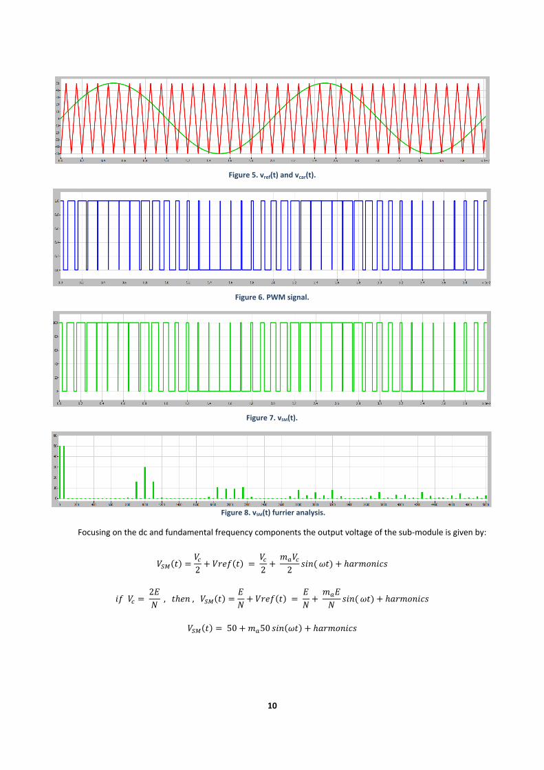
10
Figure 5. vref(t) and vcar(t).
Figure 6. PWM signal.
Figure 7. vSM(t).
Figure 8. vSM(t) furrier analysis.
Focusing on the dc and fundamental frequency components the output voltage of the sub-module is given by:
( ) ( )
( )
( )
( )
( )
( ) ( )
11
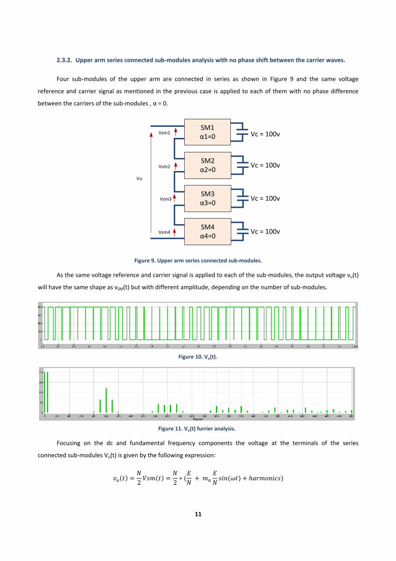
2.3.2. Upper arm series connected sub-modules analysis with no phase shift between the carrier waves.
Four sub-modules of the upper arm are connected in series as shown in Figure 9 and the same voltage
reference and carrier signal as mentioned in the previous case is applied to each of them with no phase difference
between the carriers of the sub-modules , α = 0.
SM1α1=0 Vc = 100v
SM2α2=0
SM3α3=0
SM4α4=0
Vsm1
Vsm2
Vsm3
Vsm4
Vu
Vc = 100v
Vc = 100v
Vc = 100v
Figure 9. Upper arm series connected sub-modules.
As the same voltage reference and carrier signal is applied to each of the sub-modules, the output voltage vu(t)
will have the same shape as vSM(t) but with different amplitude, depending on the number of sub-modules.
Figure 10. Vu(t).
Figure 11. Vu(t) furrier analysis.
Focusing on the dc and fundamental frequency components the voltage at the terminals of the series
connected sub-modules Vu(t) is given by the following expression:
( )
( )
(
( ) )
12
( )
( )
( ) ( )
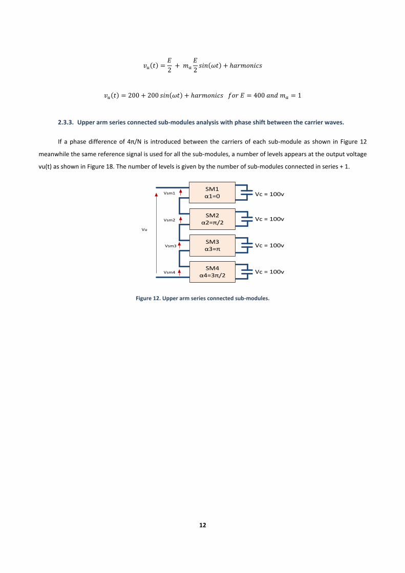
2.3.3. Upper arm series connected sub-modules analysis with phase shift between the carrier waves.
If a phase difference of 4π/N is introduced between the carriers of each sub-module as shown in Figure 12
meanwhile the same reference signal is used for all the sub-modules, a number of levels appears at the output voltage
vu(t) as shown in Figure 18. The number of levels is given by the number of sub-modules connected in series + 1.
SM1α1=0 Vc = 100v
SM2α2=π/2
SM3α3=π
SM4α4=3π/2
Vsm1
Vsm2
Vsm3
Vsm4
Vu
Vc = 100v
Vc = 100v
Vc = 100v
Figure 12. Upper arm series connected sub-modules.
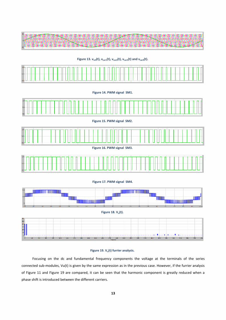
13
Figure 13. vref(t), vcar1(t), vcar2(t), vcar3(t) and vcar4(t).
Figure 14. PWM signal SM1.
Figure 15. PWM signal SM2.
Figure 16. PWM signal SM3.
Figure 17. PWM signal SM4.
Figure 18. Vu(t).
Figure 19. Vu(t) furrier analysis.
Focusing on the dc and fundamental frequency components the voltage at the terminals of the series
connected sub-modules, Vu(t) is given by the same expression as in the previous case. However, if the furrier analysis
of Figure 11 and Figure 19 are compared, it can be seen that the harmonic component is greatly reduced when a
phase shift is introduced between the different carriers.
14
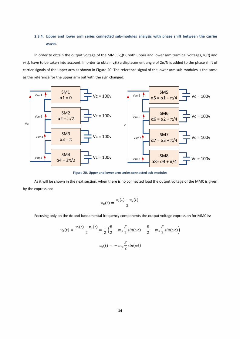
2.3.4. Upper and lower arm series connected sub-modules analysis with phase shift between the carrier
waves.
In order to obtain the output voltage of the MMC, vo(t), both upper and lower arm terminal voltages, vu(t) and
vl(t), have to be taken into account. In order to obtain vl(t) a displacement angle of 2π/N is added to the phase shift of
carrier signals of the upper arm as shown in Figure 20. The reference signal of the lower arm sub-modules is the same
as the reference for the upper arm but with the sign changed.
SM1α1 = 0 Vc = 100v
SM2α2 = π/2
SM3α3 = π
SM4α4 = 3π/2
Vsm1
Vsm2
Vsm3
Vsm4
Vu
Vc = 100v
Vc = 100v
Vc = 100v
SM5α5 = α1 + π/4 Vc = 100v
SM6α6 = α2 + π/4
SM7α7 = α3 + π/4
SM8α8= α4 + π/4
Vsm5
Vsm6
Vsm7
Vsm8
Vl
Vc = 100v
Vc = 100v
Vc = 100v
Figure 20. Upper and lower arm series connected sub-modules
As it will be shown in the next section, when there is no connected load the output voltage of the MMC is given
by the expression:
( ) ( ) ( )
Focusing only on the dc and fundamental frequency components the output voltage expression for MMC is:
( ) ( ) ( )
(
( )
( ))
( )
( )
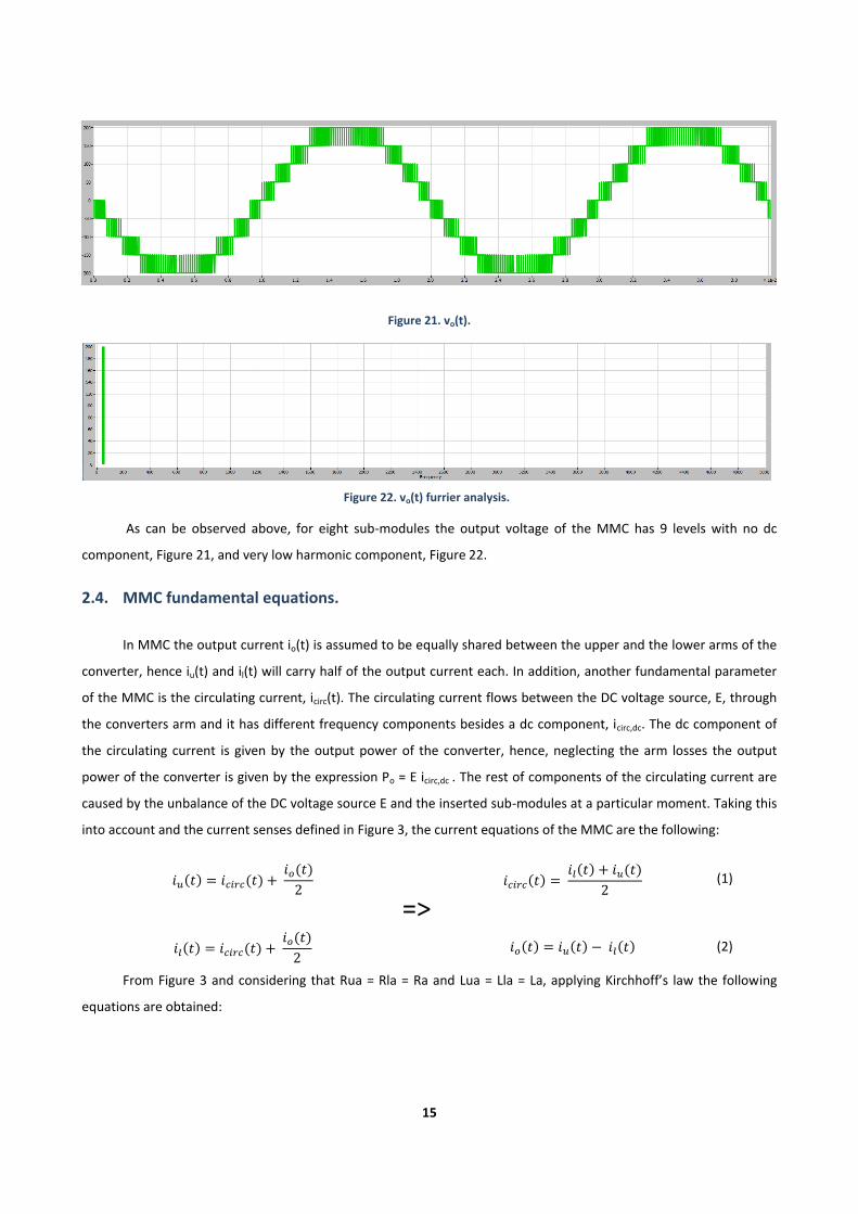
15
Figure 21. vo(t).
Figure 22. vo(t) furrier analysis.
As can be observed above, for eight sub-modules the output voltage of the MMC has 9 levels with no dc
component, Figure 21, and very low harmonic component, Figure 22.
2.4. MMC fundamental equations.
In MMC the output current io(t) is assumed to be equally shared between the upper and the lower arms of the
converter, hence iu(t) and il(t) will carry half of the output current each. In addition, another fundamental parameter
of the MMC is the circulating current, icirc(t). The circulating current flows between the DC voltage source, E, through
the converters arm and it has different frequency components besides a dc component, icirc,dc. The dc component of
the circulating current is given by the output power of the converter, hence, neglecting the arm losses the output
power of the converter is given by the expression Po = E icirc,dc . The rest of components of the circulating current are
caused by the unbalance of the DC voltage source E and the inserted sub-modules at a particular moment. Taking this
into account and the current senses defined in Figure 3, the current equations of the MMC are the following:
( ) ( )
( )
=> ( )
( ) ( )
(1)
( ) ( )
( )
( ) ( ) ( ) (2)
From Figure 3 and considering that Rua = Rla = Ra and Lua = Lla = La, applying Kirchhoff’s law the following
equations are obtained:
16
( ) ( ) ( ( ) ( ))
( ( ) ( )) (3)
( )
( )
( )
( ) (4)
( )
( )
( )
( ) (5)
From (1), (2) and (3) the equation which dictates the behavior of the circulating current is obtained:
( ) ( ( ) ( )) ( )
( )
(6)
From (1), (4) and (5) the output voltage equation of the MMC is obtained:
( ) ( ) ( )
( )
( )
( ) (7)
Combining (4), (5), (6) and (7) the equations shown below are obtained. These equations have a fundamental
importance for control purposes because they describe the reference signals for the upper and lower arm.
( )
( ) ( ) (8)
( )
( ) ( ) (9)
( )
( ) (10)
2.5. MMC control topologies.
The MMC control task for HVDC application can be very challenging due to the large number of sub-modules
present in the converter. The control tasks to be carried out for this project can be divided into the following
categories: 1) output current control in order to control active and reactive power, 2) average capacitor voltage level
control, 3) individual capacitor voltage balancing control and 4) fault tolerant control. Taking this into account two
different control approaches can be adopted: centralized control and hierarchical control [17].
The centralized control topology implies the usage of only one single controller, which is carrying out all the
needed processing and control operations. It is required to the controller to be very powerful in order to be able to
handle all the intense processing. Besides this, also a large amount of signals wires need be available [17], [21]. A
simplified scheme of the centralized control topology applied to a single phase MMC with eight sub-modules is shown
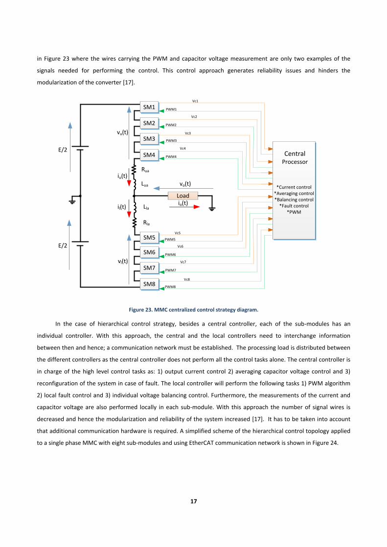
17
in Figure 23 where the wires carrying the PWM and capacitor voltage measurement are only two examples of the
signals needed for performing the control. This control approach generates reliability issues and hinders the
modularization of the converter [17].
PWM1
PWM2
PWM3
PWM4
PWM5
PWM6
PWM7
PWM8
Vc1
Vc2
Vc3
Vc4
Vc5
Vc6
Vc7
Vc8
*Current control*Averaging control*Balancing control
*Fault control*PWM
CentralProcessor
E/2
Lla
Lua
SM1
SM3
SM4
SM2
SM7
SM8
SM6
SM5E/2
Rla
Rua
Load
vu(t)
iu(t)
il(t)
vl(t)
io(t)
vo(t)
Figure 23. MMC centralized control strategy diagram.
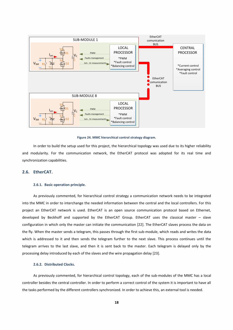
In the case of hierarchical control strategy, besides a central controller, each of the sub-modules has an
individual controller. With this approach, the central and the local controllers need to interchange information
between then and hence; a communication network must be established. The processing load is distributed between
the different controllers as the central controller does not perform all the control tasks alone. The central controller is
in charge of the high level control tasks as: 1) output current control 2) averaging capacitor voltage control and 3)
reconfiguration of the system in case of fault. The local controller will perform the following tasks 1) PWM algorithm
2) local fault control and 3) individual voltage balancing control. Furthermore, the measurements of the current and
capacitor voltage are also performed locally in each sub-module. With this approach the number of signal wires is
decreased and hence the modularization and reliability of the system increased [17]. It has to be taken into account
that additional communication hardware is required. A simplified scheme of the hierarchical control topology applied
to a single phase MMC with eight sub-modules and using EtherCAT communication network is shown in Figure 24.
18
PWM
Faults manegement
Ism , Vc measurements
SUB-MODULE 1
CENTRAL PROCESSOR
*Current control*Averaging control
*Fault control
LOCAL PROCESSOR
*PWM*Fault control
*Balancing control
PWM
Faults manegement
Ism , Vc measurements
SUB-MODULE 8
LOCAL PROCESSOR
*PWM*Fault control
*Balancing control
EtherCAT comunication
BUS
EtherCAT comunication
BUS
S1
S2
VC
VSM
Ism
C
D1
D2R1T1
S1
S2
VC
VSM
Ism
C
D1
D2R1T1
Figure 24. MMC hierarchical control strategy diagram.
In order to build the setup used for this project, the hierarchical topology was used due to its higher reliability
and modularity. For the communication network, the EtherCAT protocol was adopted for its real time and
synchronization capabilities.
2.6. EtherCAT.
2.6.1. Basic operation principle.
As previously commented, for hierarchical control strategy a communication network needs to be integrated
into the MMC in order to interchange the needed information between the central and the local controllers. For this
project an EtherCAT network is used. EtherCAT is an open source communication protocol based on Ethernet,
developed by Beckhoff and supported by the EtherCAT Group. EtherCAT uses the classical master – slave
configuration in which only the master can initiate the communication [22]. The EtherCAT slaves process the data on
the fly. When the master sends a telegram, this passes through the first sub-module, which reads and writes the data
which is addressed to it and then sends the telegram further to the next slave. This process continues until the
telegram arrives to the last slave, and then it is sent back to the master. Each telegram is delayed only by the
processing delay introduced by each of the slaves and the wire propagation delay [23].
2.6.2. Distributed Clocks.
As previously commented, for hierarchical control topology, each of the sub-modules of the MMC has a local
controller besides the central controller. In order to perform a correct control of the system it is important to have all
the tasks performed by the different controllers synchronized. In order to achieve this, an external tool is needed.
19
‘Distributed clocks’ is an EtherCAT protocol feature which can be used for generating of synchronous output
signals with very low jitter and high precision clock synchronization. Each of the EtherCAT slaves is equipped with an
internal clock. It is desired the time of these clocks to be the same; however differences between them may exist due
to the following reasons. In first place when the slaves are turned-on the register in which the current time is hold is
set to zero, however an initial offset between them will exist because the set to zero does not happen at the same
time in all slaves. In second place, the internal differences of the slave’s oscillators will lead to a drift between the
different clocks.
The Distributed Clocks algorithm is a mechanism to synchronize all the clocks of the sub-modules with a
reference clock, which is usually the clock of the first slave. In order to do this, the propagation delay of each slave,
the initial time offsets and the different local drifts are calculated and then compensated. By means of synchronizing
the internal clocks of the slaves the EtherCAT network is able to generate synchronized outputs with a jitter down to
nanoseconds. This is a key feature for the synchronization of the MMC sub-modules.
2.6.3. Galvanic isolation.
In case of a fault in the MMC a very potential difference could drop on one or more sub-modules. Without the
proper isolation this high voltage could cause serious damages in the different components of the system. As
EtherCAT uses optic fibers for communication instead or electric wires the different elements connected to the
network are galvanically isolated.
2.6.4. Integration of EtherCAT in the MMC design
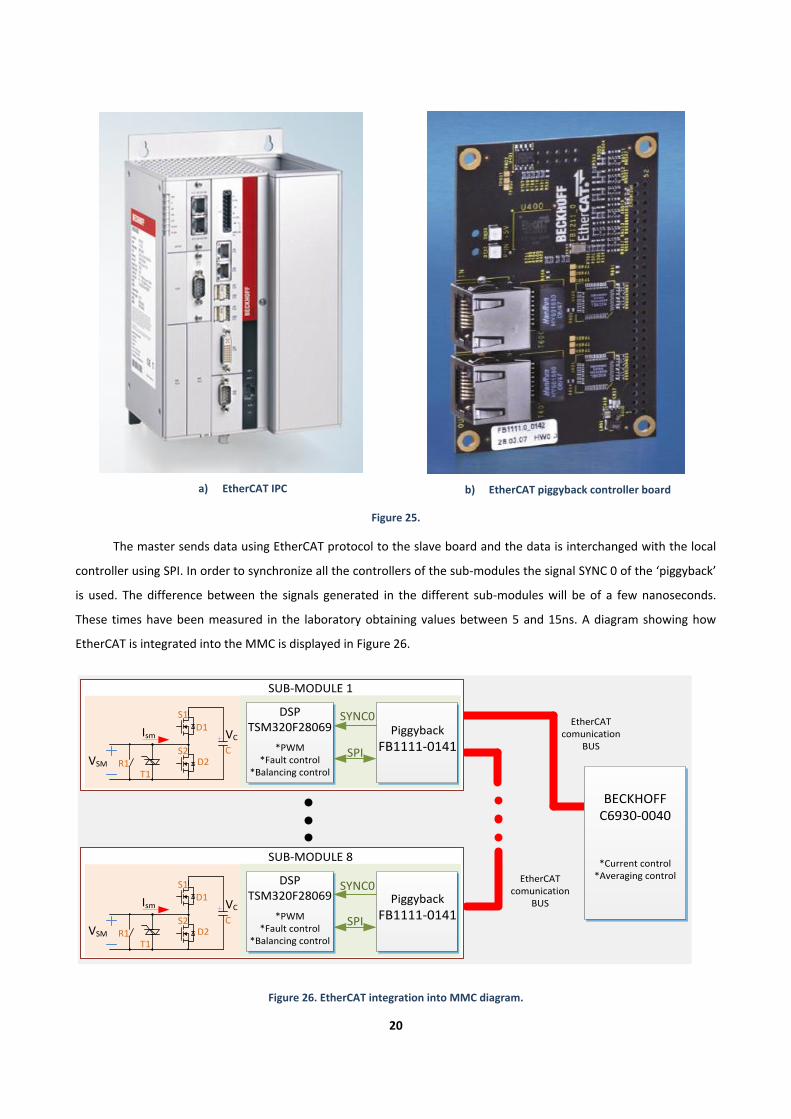
In order to integrate the EtherCAT communication network into the small scale MMC the following
commercially available products were used. As master of the network a ‘BECKHOFF C 9030-0040’ industrial PC, Figure
25 a, was employed along with the software TwinCAT 3.1 in order to program the high level control tasks. The
‘BECKHOFF piggyback FB1111-0141’, Figure 25 b, was utilized as a slave board. These boards allow SPI communication
with the local controller.
20
a) EtherCAT IPC
b) EtherCAT piggyback controller board
Figure 25.
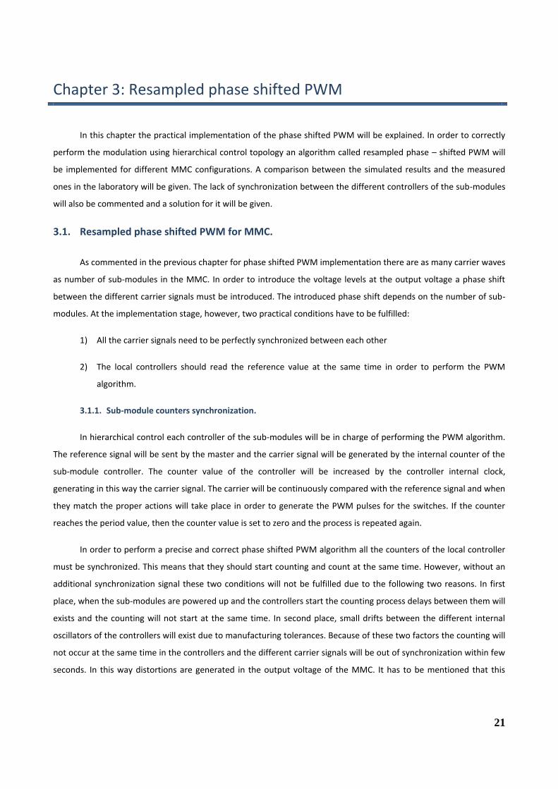
The master sends data using EtherCAT protocol to the slave board and the data is interchanged with the local
controller using SPI. In order to synchronize all the controllers of the sub-modules the signal SYNC 0 of the ‘piggyback’
is used. The difference between the signals generated in the different sub-modules will be of a few nanoseconds.
These times have been measured in the laboratory obtaining values between 5 and 15ns. A diagram showing how
EtherCAT is integrated into the MMC is displayed in Figure 26.
EtherCAT comunication
BUS
EtherCAT comunication
BUS
BECKHOFF C6930-0040
*Current control*Averaging control
SUB-MODULE 1
DSPTSM320F28069
*PWM*Fault control
*Balancing control
Piggyback
FB1111-0141SPI
SYNC0
SUB-MODULE 8
DSPTSM320F28069
*PWM*Fault control
*Balancing control
Piggyback
FB1111-0141SPI
SYNC0
S1
S2
VC
VSM
Ism
C
D1
D2R1T1
S1
S2
VC
VSM
Ism
C
D1
D2R1T1
Figure 26. EtherCAT integration into MMC diagram.
21
Chapter 3: Resampled phase shifted PWM
In this chapter the practical implementation of the phase shifted PWM will be explained. In order to correctly
perform the modulation using hierarchical control topology an algorithm called resampled phase – shifted PWM will
be implemented for different MMC configurations. A comparison between the simulated results and the measured
ones in the laboratory will be given. The lack of synchronization between the different controllers of the sub-modules
will also be commented and a solution for it will be given.
3.1. Resampled phase shifted PWM for MMC.
As commented in the previous chapter for phase shifted PWM implementation there are as many carrier waves
as number of sub-modules in the MMC. In order to introduce the voltage levels at the output voltage a phase shift
between the different carrier signals must be introduced. The introduced phase shift depends on the number of sub-
modules. At the implementation stage, however, two practical conditions have to be fulfilled:
1) All the carrier signals need to be perfectly synchronized between each other
2) The local controllers should read the reference value at the same time in order to perform the PWM
algorithm.
3.1.1. Sub-module counters synchronization.
In hierarchical control each controller of the sub-modules will be in charge of performing the PWM algorithm.
The reference signal will be sent by the master and the carrier signal will be generated by the internal counter of the
sub-module controller. The counter value of the controller will be increased by the controller internal clock,
generating in this way the carrier signal. The carrier will be continuously compared with the reference signal and when
they match the proper actions will take place in order to generate the PWM pulses for the switches. If the counter
reaches the period value, then the counter value is set to zero and the process is repeated again.
In order to perform a precise and correct phase shifted PWM algorithm all the counters of the local controller
must be synchronized. This means that they should start counting and count at the same time. However, without an
additional synchronization signal these two conditions will not be fulfilled due to the following two reasons. In first
place, when the sub-modules are powered up and the controllers start the counting process delays between them will
exists and the counting will not start at the same time. In second place, small drifts between the different internal
oscillators of the controllers will exist due to manufacturing tolerances. Because of these two factors the counting will
not occur at the same time in the controllers and the different carrier signals will be out of synchronization within few
seconds. In this way distortions are generated in the output voltage of the MMC. It has to be mentioned that this
22
problem is only given in hierarchical control. When using centralized control topology a single oscillator is used to
generate all the PWM outputs and hence, the signals will be synchronized.
In order to synchronize the counters of all the local controllers a method based on the usage of EtherCAT
‘Distributed Clocks’ mechanism has been implemented. The local controller used for MMC system is a TMS320F28069
Texas Instruments MCU which is connected to the ‘piggyback’ EtherCAT slave board. The slave board digital pin for
generating synchronized events, SYNC0, is connected to one of the local controller inputs. Because of the ‘Distributed
Clocks’ feature, each slave is able to generate a synchronized cyclic event through the SYNC0 pin. The differences
between the generated signals have been measured in the laboratory obtaining values in the range of 5 to 15ns. In
order to correctly perform the synchronization, the cycle period of the SYNCH0 event has to match the local controller
counter period. SYNC0 will usually be at a high state, however when a cycle period is completed it will go to a low
state for a very short time. This falling edge will generate an external interrupt in the local controller and the value of
the counter will be set to 0.
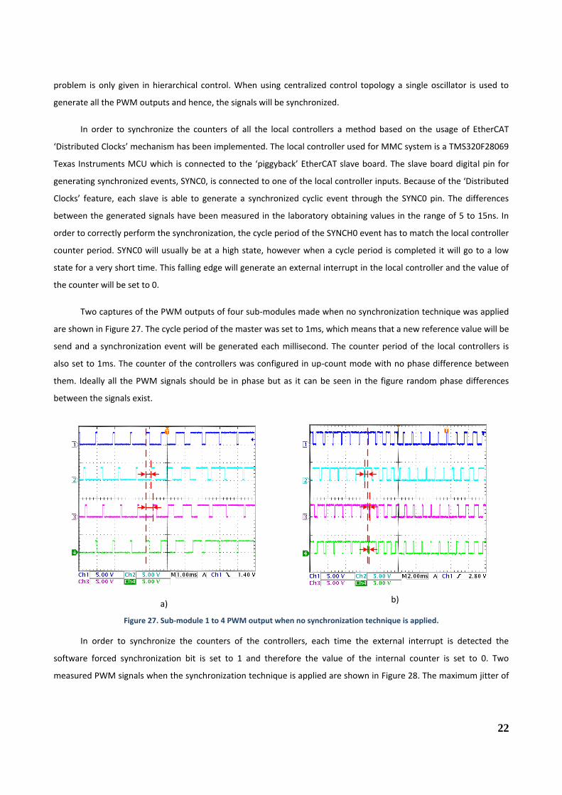
Two captures of the PWM outputs of four sub-modules made when no synchronization technique was applied
are shown in Figure 27. The cycle period of the master was set to 1ms, which means that a new reference value will be
send and a synchronization event will be generated each millisecond. The counter period of the local controllers is
also set to 1ms. The counter of the controllers was configured in up-count mode with no phase difference between
them. Ideally all the PWM signals should be in phase but as it can be seen in the figure random phase differences
between the signals exist.
a)
b)
Figure 27. Sub-module 1 to 4 PWM output when no synchronization technique is applied.
In order to synchronize the counters of the controllers, each time the external interrupt is detected the
software forced synchronization bit is set to 1 and therefore the value of the internal counter is set to 0. Two
measured PWM signals when the synchronization technique is applied are shown in Figure 28. The maximum jitter of
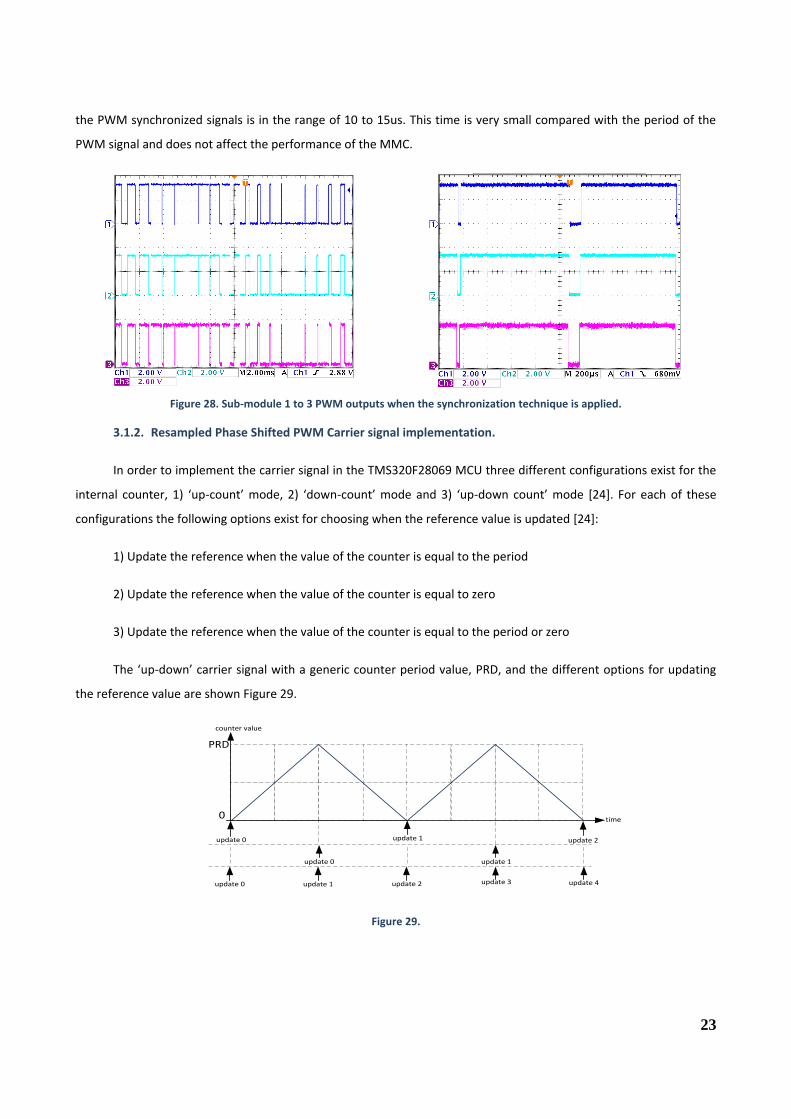
23
the PWM synchronized signals is in the range of 10 to 15us. This time is very small compared with the period of the
PWM signal and does not affect the performance of the MMC.
Figure 28. Sub-module 1 to 3 PWM outputs when the synchronization technique is applied.
3.1.2. Resampled Phase Shifted PWM Carrier signal implementation.
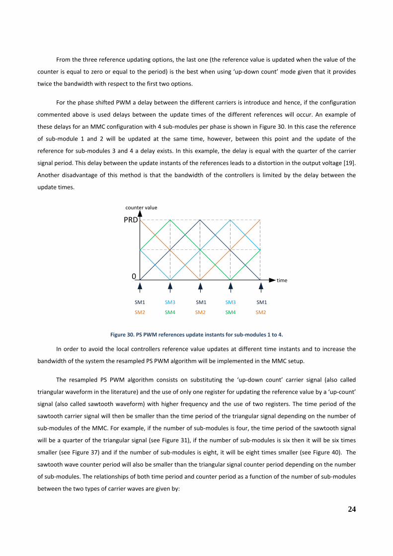
In order to implement the carrier signal in the TMS320F28069 MCU three different configurations exist for the
internal counter, 1) ‘up-count’ mode, 2) ‘down-count’ mode and 3) ‘up-down count’ mode [24]. For each of these
configurations the following options exist for choosing when the reference value is updated [24]:
1) Update the reference when the value of the counter is equal to the period
2) Update the reference when the value of the counter is equal to zero
3) Update the reference when the value of the counter is equal to the period or zero
The ‘up-down’ carrier signal with a generic counter period value, PRD, and the different options for updating
the reference value are shown Figure 29.
PRD
0
update 0 update 1 update 2
update 0 update 1
update 0 update 1 update 2 update 3 update 4
counter value
time
Figure 29.
24
From the three reference updating options, the last one (the reference value is updated when the value of the
counter is equal to zero or equal to the period) is the best when using ‘up-down count’ mode given that it provides
twice the bandwidth with respect to the first two options.
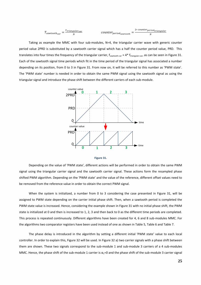
For the phase shifted PWM a delay between the different carriers is introduce and hence, if the configuration
commented above is used delays between the update times of the different references will occur. An example of
these delays for an MMC configuration with 4 sub-modules per phase is shown in Figure 30. In this case the reference
of sub-module 1 and 2 will be updated at the same time, however, between this point and the update of the
reference for sub-modules 3 and 4 a delay exists. In this example, the delay is equal with the quarter of the carrier
signal period. This delay between the update instants of the references leads to a distortion in the output voltage [19].
Another disadvantage of this method is that the bandwidth of the controllers is limited by the delay between the
update times.
PRD
0
SM1
SM2
SM1
SM2
SM1
SM2
SM3 SM3
SM4 SM4
counter value
time
Figure 30. PS PWM references update instants for sub-modules 1 to 4.
In order to avoid the local controllers reference value updates at different time instants and to increase the
bandwidth of the system the resampled PS PWM algorithm will be implemented in the MMC setup.
The resampled PS PWM algorithm consists on substituting the ‘up-down count’ carrier signal (also called
triangular waveform in the literature) and the use of only one register for updating the reference value by a ‘up-count’
signal (also called sawtooth waveform) with higher frequency and the use of two registers. The time period of the
sawtooth carrier signal will then be smaller than the time period of the triangular signal depending on the number of
sub-modules of the MMC. For example, if the number of sub-modules is four, the time period of the sawtooth signal
will be a quarter of the triangular signal (see Figure 31), if the number of sub-modules is six then it will be six times
smaller (see Figure 37) and if the number of sub-modules is eight, it will be eight times smaller (see Figure 40). The
sawtooth wave counter period will also be smaller than the triangular signal counter period depending on the number
of sub-modules. The relationships of both time period and counter period as a function of the number of sub-modules
between the two types of carrier waves are given by:
25
Taking as example the MMC with four sub-modules, N=4, the triangular carrier wave with generic counter
period value 2PRD is substituted by a sawtooth carrier signal which has a half the counter period value, PRD. This
translates into four times the frequency of the triangular carrier, fsawtooth-car = 4* ftriangular-car, as can be seen in Figure 31.
Each of the sawtooth signal time periods which fit in the time period of the triangular signal has associated a number
depending on its position, from 0 to 3 in Figure 31. From now on, it will be referred to this number as ‘PWM state’.
The ‘PWM state’ number is needed in order to obtain the same PWM signal using the sawtooth signal as using the
triangular signal and introduce the phase shift between the different carriers of each sub-module.
PRD
2PRD 0 1 2 3
0
PRD
00 1 2 3
counter value
counter value
time
time
Figure 31.
Depending on the value of ‘PWM state’, different actions will be performed in order to obtain the same PWM
signal using the triangular carrier signal and the sawtooth carrier signal. These actions form the resampled phase
shifted PWM algorithm. Depending on the ‘PWM state’ and the value of the reference, different offset values need to
be removed from the reference value in order to obtain the correct PWM signal.
When the system is initialized, a number from 0 to 3 considering the case presented in Figure 31, will be
assigned to PWM state depending on the carrier initial phase shift. Then, when a sawtooth period is completed the
PWM state value is increased. Hence, considering the example shown in Figure 31 with no initial phase shift, the PWM
state is initialized at 0 and then is increased to 1, 2, 3 and then back to 0 as the different time periods are completed.
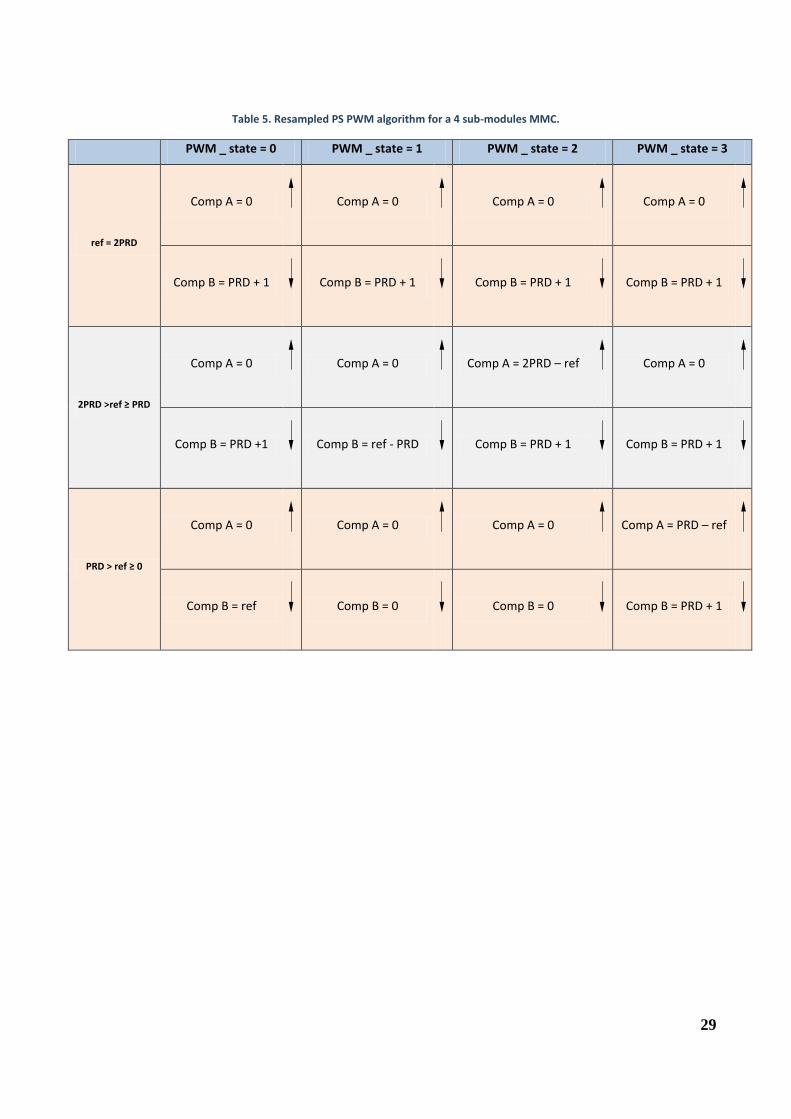
This process is repeated continuously. Different algorithms have been created for 4, 6 and 8 sub-modules MMC. For
the algorithms two comparator registers have been used instead of one as shown in Table 5, Table 6 and Table 7.
The phase delay is introduced in the algorithm by setting a different initial ‘PWM state’ value to each local
controller. In order to explain this, Figure 32 will be used. In Figure 32 a) two carrier signals with a phase shift between
them are shown. These two signals correspond to the sub-module 1 and sub-module 3 carriers of a 4 sub-modules
MMC. Hence, the phase shift of the sub-module 1 carrier is α1=0 and the phase shift of the sub-module 3 carrier signal
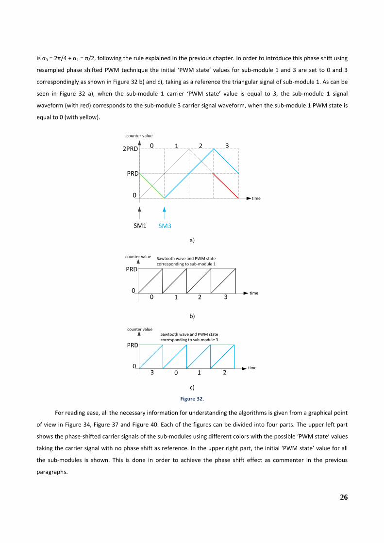
26
is α3 = 2π/4 + α1 = π/2, following the rule explained in the previous chapter. In order to introduce this phase shift using
resampled phase shifted PWM technique the initial ‘PWM state’ values for sub-module 1 and 3 are set to 0 and 3
correspondingly as shown in Figure 32 b) and c), taking as a reference the triangular signal of sub-module 1. As can be
seen in Figure 32 a), when the sub-module 1 carrier ‘PWM state’ value is equal to 3, the sub-module 1 signal
waveform (with red) corresponds to the sub-module 3 carrier signal waveform, when the sub-module 1 PWM state is
equal to 0 (with yellow).
PRD
2PRD 0 1 2 3
0
SM1 SM3
counter value
time
a)
PRD
00 1 2 3
time
Sawtooth wave and PWM state corresponding to sub-module 1
counter value
b)
PRD
03 0 1 2
time
Sawtooth wave and PWM state corresponding to sub-module 3
counter value
c)
Figure 32.
For reading ease, all the necessary information for understanding the algorithms is given from a graphical point
of view in Figure 34, Figure 37 and Figure 40. Each of the figures can be divided into four parts. The upper left part
shows the phase-shifted carrier signals of the sub-modules using different colors with the possible ‘PWM state’ values
taking the carrier signal with no phase shift as reference. In the upper right part, the initial ‘PWM state’ value for all
the sub-modules is shown. This is done in order to achieve the phase shift effect as commenter in the previous
paragraphs.
27
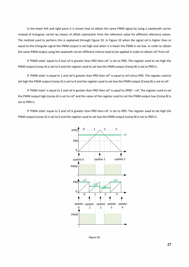
In the lower left and right parts it is shown how to obtain the same PWM signal by using a sawthooth carrier
instead of triangular carrier by means of offset subtraction from the reference value for different reference values.
The method used to perform this is explained through Figure 33. In Figure 33 when the signal ref is higher than or
equal to the triangular signal the PWM output is set high and when it is lower the PWM is set low. In order to obtain
the same PWM output using the sawtooth carrier different criteria need to be applied in order to obtain ref’ from ref.
If ‘PWM state’ equal to 0 and ref is greater than PRD then ref´ is set to PRD. The register used to set high the
PWM output (comp A) is set to 0 and the register used to set low the PWM output (Comp B) is set to PRD+1.
If ´PWM state’ is equal to 1 and ref is greater than PRD then ref’ is equal to ref minus PRD. The register used to
set high the PWM output (comp A) is set to 0 and the register used to set low the PWM output (Comp B) is set to ref’.
If ‘PWM state’ is equal to 2 and ref is greater than PRD then ref’ is equal to 2PRD – ref. The register used to set
the PWM output high (comp A) is set to ref’ and the value of the register used to set the PWM output low (Comp B) is
set to PRD+1.
If ‘PWM state’ equal to 3 and ref is greater than PRD then ref´ is set to PRD. The register used to set high the
PWM output (comp A) is set to 0 and the register used to set low the PWM output (comp B) is set to PRD+1.
PRD
PRD
2PRD
ref
PWM
0 1 2 3
0
0
ref'
ref'ref'
ref'
0 1 2 3
PWM
update 0 update 1 update 2
update 0
update 1
update 2
update3
update4
Figure 33.
28
The same procedure as commented above is used for different reference values and for different number of
sub-module obtaining the resampled PS PWM algorithm. The algorithms are given in Table 5, Table 6 and Table 7.
After each explanation of the algorithm a capture of the PMM signal measured in the laboratory using the resampled
method is presented and compared with the PS PWM signals obtained by simulations. As it can be observed in those
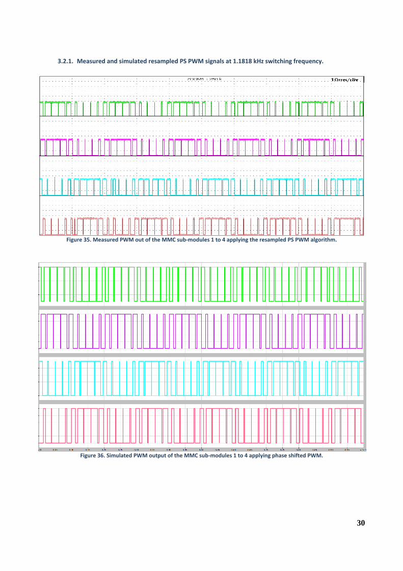
plots, besides small differences in certain cases, the results obtained in the laboratory are the same as the results
obtained in the simulations.
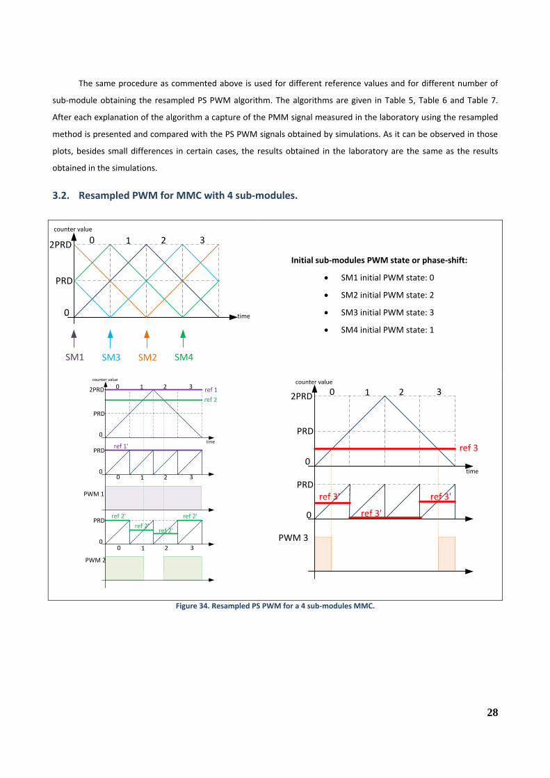
3.2. Resampled PWM for MMC with 4 sub-modules.
PRD
2PRD 0 1 2 3
0
SM1 SM3 SM2 SM4
counter value
time
Initial sub-modules PWM state or phase-shift:
SM1 initial PWM state: 0
SM2 initial PWM state: 2
SM3 initial PWM state: 3
SM4 initial PWM state: 1
PRD
PRD
2PRD
ref 2
PWM 2
0 1 2 3
0
0
ref 1
ref 2'
ref 2'ref 2'
ref 2'
PRD
PWM 1
0
ref 1'
0 1 2 3
0 1 2 3
counter value
time
PRD
PRD
2PRD
ref 3
PWM 3
0 1 2 3
0
0
ref 3'ref 3'
ref 3'
counter value
time
Figure 34. Resampled PS PWM for a 4 sub-modules MMC.
29
Table 5. Resampled PS PWM algorithm for a 4 sub-modules MMC.
PWM _ state = 0 PWM _ state = 1 PWM _ state = 2 PWM _ state = 3
ref = 2PRD
Comp A = 0
Comp A = 0
Comp A = 0
Comp A = 0
Comp B = PRD + 1
Comp B = PRD + 1
Comp B = PRD + 1
Comp B = PRD + 1
2PRD >ref ≥ PRD
Comp A = 0
Comp A = 0
Comp A = 2PRD – ref
Comp A = 0
Comp B = PRD +1
Comp B = ref - PRD
Comp B = PRD + 1
Comp B = PRD + 1
PRD > ref ≥ 0
Comp A = 0
Comp A = 0
Comp A = 0
Comp A = PRD – ref
Comp B = ref
Comp B = 0
Comp B = 0
Comp B = PRD + 1
30
3.2.1. Measured and simulated resampled PS PWM signals at 1.1818 kHz switching frequency.
Figure 35. Measured PWM out of the MMC sub-modules 1 to 4 applying the resampled PS PWM algorithm.
Figure 36. Simulated PWM output of the MMC sub-modules 1 to 4 applying phase shifted PWM.
31
3.3. Resampled PWM for MMC with 6 sub-modules.
PRD
2PRD
0 1 2 33PRD
4 5
0
SM1SM4
SM2SM5
SM3SM6
SM1SM4
counter value
time
Initial sub-modules PWM state or phase-shift:
SM1 initial PWM state: 0
SM2 initial PWM state: 4
SM3 initial PWM state: 2
SM4 initial PWM state: 0
SM5 initial PWM state: 4
SM6 initial PWM state: 2
PRD
2PRD
0 1 2 33PRD
4 5
PWM 2
ref 2
PRD ref 2'
ref 2'ref 2'
ref 2'
0
00 1 2 3 4 5
ref 1
PWM 1
PRD ref 1'
00 1 2 3 4 5
counter value
time
PRD
PRD
2PRD
ref 4
PWM 4
0 1 2 33PRD
4 5
ref 4' ref 4'
ref 4'
0
00 1 2 3 4 5
PRD
ref 3
PWM 3
ref 3'
ref 3' ref 3'
ref 3' ref 3'
00 1 2 3 4 5
counter value
time
Figure 37. Resampled PS PWM for a 4 sub-modules MMC.
32
Table 6. Resampled PS PWM algorithm for a 6 sub-modules MMC.
PWM_state = 0 PWM_state = 1 PWM_state = 2 PWM_state = 3 PWM_state = 4 PWM_state = 5
ref = 3PRD
Comp A = 0
Comp A = 0
Comp A = 0
Comp A = 0
Comp A = 0
Comp A = 0
Comp B = PRD +1
Comp B = PRD+1
Comp B = PRD+1
Comp B PRD + 1
Comp B = PRD +1
Comp B = PRD +1
3PRD > ref ≥ 2PRD
Comp A = 0
Comp A = 0
Comp A = 0
Comp A = 3PRD – ref
Comp A = 0
Comp A = 0
Comp B = PRD +1
Comp B = PRD+1
Comp B = ref – 2PRD
Comp B = PRD + 1
Comp B = PRD +1
Comp B = PRD +1
2PRD > ref ≥ PRD
Comp A = 0
Comp A = 0
Comp A = 0
Comp A = 0
Comp A = 2PRD – ref
Comp A = 0
Comp B = PRD +1
Comp B = ref - PRD
Comp B = 0
Comp B = 0
Comp B = PRD +1
Comp B = PRD +1
33
PWM_state = 0 PWM_state = 1 PWM_state = 2 PWM_state = 3 PWM_state = 4 PWM_state = 5
PRD > ref ≥ 0
Comp A = 0
Comp A = 0
Comp A = 0
Comp A = 0
Comp A = 0
Comp A = PRD – ref
Comp B = ref
Comp B = 0
Comp B = 0
Comp B = 0
Comp B = 0
Comp B = PRD + 1
34
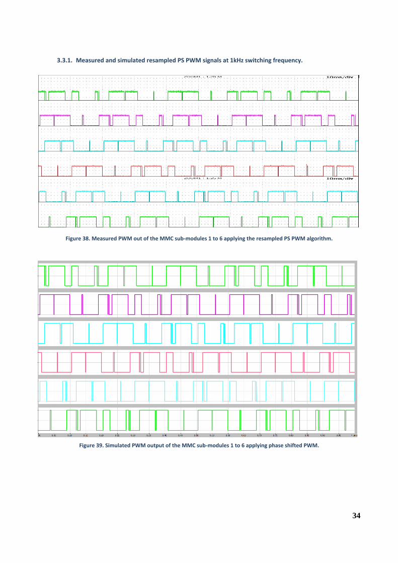
3.3.1. Measured and simulated resampled PS PWM signals at 1kHz switching frequency.
Figure 38. Measured PWM out of the MMC sub-modules 1 to 6 applying the resampled PS PWM algorithm.
Figure 39. Simulated PWM output of the MMC sub-modules 1 to 6 applying phase shifted PWM.
35
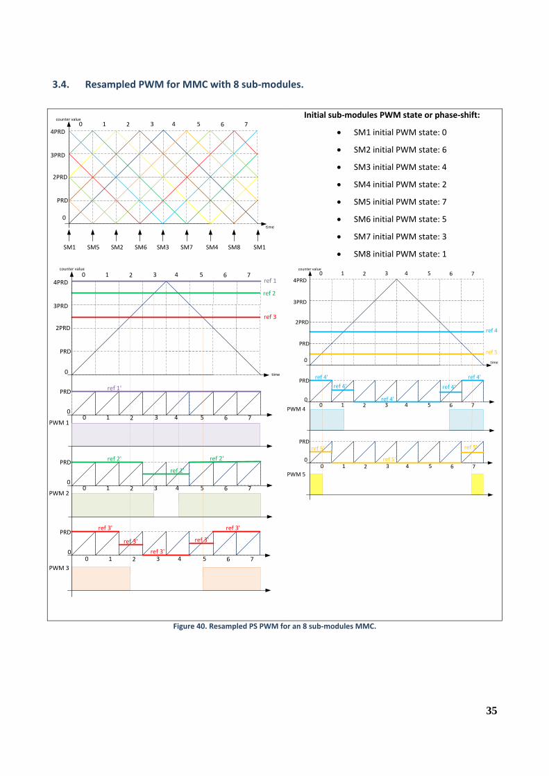
3.4. Resampled PWM for MMC with 8 sub-modules.
PRD
2PRD
0 1 2 3
3PRD
4 5 6 74PRD
0
SM1 SM5 SM2 SM6 SM3 SM7 SM4 SM8 SM1
counter value
time
Initial sub-modules PWM state or phase-shift:
SM1 initial PWM state: 0
SM2 initial PWM state: 6
SM3 initial PWM state: 4
SM4 initial PWM state: 2
SM5 initial PWM state: 7
SM6 initial PWM state: 5
SM7 initial PWM state: 3
SM8 initial PWM state: 1
PRD
PRD
2PRD
ref 3
PWM 3
0 1 2 3
3PRD
4 5
PWM 2
ref 2
PRD
6 74PRD
ref 2'
ref 2'
ref 2'
ref 3' ref 3'
ref 3'
0 1 2 3 4 5 6 7
0 1 2 3 4 5 6 7
0
0
0
ref 1
PWM 1
PRD ref 1'
0 1 2 3 4 5 6 70
counter value
time
ref 3' ref 3'
PRD
PRD
2PRD
ref 5
PWM 5
0 1 2 3
3PRD
4 5
PWM 4
ref 4
PRD
6 74PRD
ref 4'
ref 4'
ref 4'
ref 5'
ref 5'
ref 5'
0
0
00 1 2 3 4 5 6 7
0 1 2 3 4 5 6 7
ref 4'ref 4'
counter value
time
Figure 40. Resampled PS PWM for an 8 sub-modules MMC.
36
Table 7. Resampled PS PWM algorithm for an 8 sub-modules MMC.
PWM_state = 0 PWM_state = 1 PWM_state = 2 PWM_state = 3 PWM_state = 4 PWM_state = 5 PWM_state = 6 PWM_state = 7
ref = 4PRD
Comp A = 0
Comp A = 0
Comp A = 0
Comp A = 0
Comp A = 0
Comp A = 0
Comp A = 0
Comp A = 0
Comp B = PRD +1
Comp B = PRD +1
Comp B = PRD +1
Comp B = PRD +1
Comp B = PRD +1
Comp B = PRD +1
Comp B = PRD +1
Comp B = PRD +1
4PRD > ref≥ 3PRD
Comp A = 0
Comp A = 0
Comp A = 0
Comp A = 0
Comp A = 4PRD – ref
Comp A = 0
Comp A = 0
Comp A = 0
Comp B = PRD +1
Comp B = PRD+1
Comp B = PRD+1
Comp B = ref – 3PRD
Comp B = PRD +1
Comp B = PRD +1
Comp B = PRD +1
Comp B = PRD +1
3PRD > ref≥ 2PRD
Comp A = 0
Comp A = 0
Comp A =0
Comp A = 0
Comp A = 0
Comp A = 3PRD - ref
Comp A = 0
Comp A = 0
Comp B = PRD +1
Comp B = PRD +1
Comp B = ref –
2PRD
Comp B = 0
Comp B = 0
Comp B = PRD +1
Comp B = PRD +1
Comp B = PRD +1
37
PWM_state = 0 PWM_state = 1 PWM_state = 2 PWM_state = 3 PWM_state = 4 PWM_state = 5 PWM_state = 6 PWM_state = 7
2PRD > ref ≥ PRD
Comp A = 0
Comp A = 0
Comp A = 0
Comp A = 0
Comp A = 0
Comp A = 0
Comp A =2PRD -
ref
Comp A = 0
Comp B = PRD + 1
Comp B = ref - PRD
Comp B = 0
Comp B = 0
Comp B = 0
Comp B = 0
Comp B = PRD + 1
Comp B = PRD + 1
PRD > ref ≥ 0
Comp A = 0
Comp A = 0
Comp A = 0
Comp A = 0
Comp A = 0
Comp A = 0
Comp A = 0
Comp A = PRD - ref
Comp B = ref
Comp B = 0
Comp B = 0
Comp B = 0
Comp B = 0
Comp B = 0
Comp B = 0
Comp B = PRD + 1
38
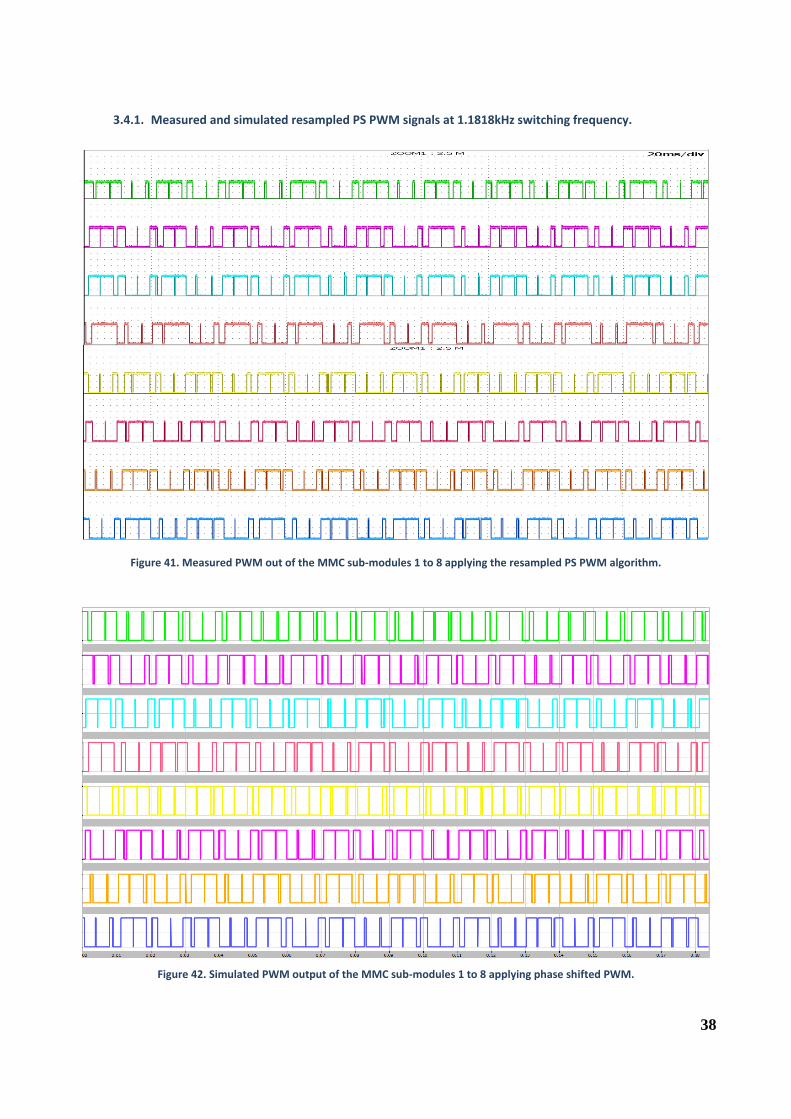
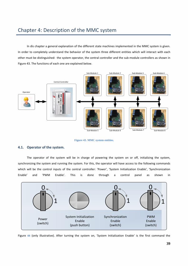
3.4.1. Measured and simulated resampled PS PWM signals at 1.1818kHz switching frequency.
Figure 41. Measured PWM out of the MMC sub-modules 1 to 8 applying the resampled PS PWM algorithm.
Figure 42. Simulated PWM output of the MMC sub-modules 1 to 8 applying phase shifted PWM.
39
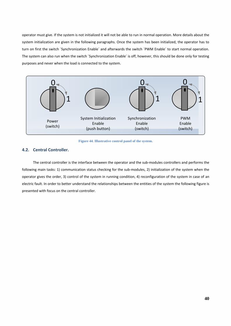
Chapter 4: Description of the MMC system
In dis chapter a general explanation of the different state machines implemented in the MMC system is given.
In order to completely understand the behavior of the system three different entities which will interact with each
other must be distinguished: the system operator, the central controller and the sub-module controllers as shown in
Figure 43. The functions of each one are explained below.
Central Controller
Operator
Sub-Module 1 Sub-Module 2 Sub-Module 3 Sub-Module 4
Sub-Module 5 Sub-Module 6 Sub-Module 7 Sub-Module 8
Figure 43. MMC system entities.
4.1. Operator of the system.
The operator of the system will be in charge of powering the system on or off, initializing the system,
synchronizing the system and running the system. For this, the operator will have access to the following commands
which will be the control inputs of the central controller: ‘Power’, ‘System Initialization Enable’, ‘Synchronization
Enable’ and ‘PWM Enable’. This is done through a control panel as shown in
1
0
System InitializationEnable
(push button)
PWMEnable
(switch)
1
0
SynchronizationEnable
(switch)
1
0
Power(switch)
Figure 44 (only illustrative). After turning the system on, ‘System Initialization Enable’ is the first command the
40
operator must give. If the system is not initialized it will not be able to run in normal operation. More details about the
system initialization are given in the following paragraphs. Once the system has been initialized, the operator has to
turn on first the switch ´Synchronization Enable´ and afterwards the switch ´PWM Enable´ to start normal operation.
The system can also run when the switch ´Synchronization Enable´ is off, however, this should be done only for testing
purposes and never when the load is connected to the system.
1
0
System InitializationEnable
(push button)
PWMEnable
(switch)
1
0
SynchronizationEnable
(switch)
1
0
Power(switch)
Figure 44. Illustrative control panel of the system.
4.2. Central Controller.
The central controller is the interface between the operator and the sub-modules controllers and performs the
following main tasks: 1) communication status checking for the sub-modules, 2) initialization of the system when the
operator gives the order, 3) control of the system in running condition, 4) reconfiguration of the system in case of an
electric fault. In order to better understand the relationships between the entities of the system the following figure is
presented with focus on the central controller.
41
1.CommandsOperator master
System Operator
Sub-module controller
Slave number 1
Sub-module controller
Slave number N
2.Damaged
Sub-Module
.
.
.
A/DExternal
Slave
1. Upper arm current
measurement
2. Lower arm current
measurement
1. By-passed state
2. Initial PWM state
5. Number of phase sub-modules
4. Voltage reference
3. Commands master- slave
Central controller
and master of the
network
number of variables = 5 x N
1. Capacitor voltage measurement
1. Capacitor voltage measurement
number of variables = 1 x N
EtherCAT communication
bus
EtherCAT communication
bus
number of variables = 2
number of variables = 1
number of variables = 1
number of variables = 5
number of variables = 5
EtherCAT communication
bus
number of variables = 2
EtherCAT communication bus
.
.
.
1. Inputs of the central controller
Colors Legend
1. Outputs of the central controller
Figure 45. MMC system entities relationships diagram.
The central controller has the following input variables from the different entities of the system:
System Operator:
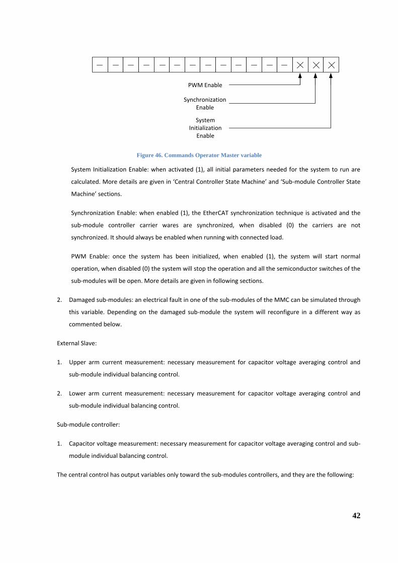
1. Commands operator master: a 16 bits variable from which the first three bits are used to transmit the
commands ‘System Initialization Enable’, ‘Synchronization Enable’ and ‘PWM Enable’ as shown in Figure
46.
42
PWM Enable
Synchronization Enable
System Initialization
Enable
Figure 46. Commands Operator Master variable
System Initialization Enable: when activated (1), all initial parameters needed for the system to run are
calculated. More details are given in ‘Central Controller State Machine’ and ‘Sub-module Controller State
Machine’ sections.
Synchronization Enable: when enabled (1), the EtherCAT synchronization technique is activated and the
sub-module controller carrier wares are synchronized, when disabled (0) the carriers are not
synchronized. It should always be enabled when running with connected load.
PWM Enable: once the system has been initialized, when enabled (1), the system will start normal
operation, when disabled (0) the system will stop the operation and all the semiconductor switches of the
sub-modules will be open. More details are given in following sections.
2. Damaged sub-modules: an electrical fault in one of the sub-modules of the MMC can be simulated through
this variable. Depending on the damaged sub-module the system will reconfigure in a different way as
commented below.
External Slave:
1. Upper arm current measurement: necessary measurement for capacitor voltage averaging control and
sub-module individual balancing control.
2. Lower arm current measurement: necessary measurement for capacitor voltage averaging control and
sub-module individual balancing control.
Sub-module controller:
1. Capacitor voltage measurement: necessary measurement for capacitor voltage averaging control and sub-
module individual balancing control.
The central control has output variables only toward the sub-modules controllers, and they are the following:
43
1. By-passed state: if a communication error is detected in the network the master may need to by-pass the
sub-module in order to perform a correct resampled PS PWM given that the number or operational sub-
modules in both arms must be always equal.
2. Initial PWM state: this variable indicates the initial phase shift of each sub-module.
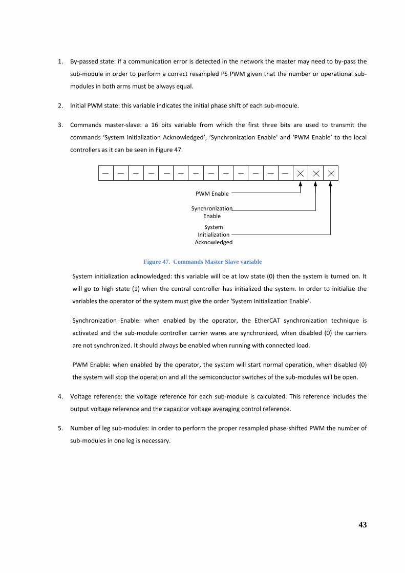
3. Commands master-slave: a 16 bits variable from which the first three bits are used to transmit the
commands ‘System Initialization Acknowledged’, ‘Synchronization Enable’ and ‘PWM Enable’ to the local
controllers as it can be seen in Figure 47.
PWM Enable
Synchronization Enable
System Initialization
Acknowledged
Figure 47. Commands Master Slave variable
System initialization acknowledged: this variable will be at low state (0) then the system is turned on. It
will go to high state (1) when the central controller has initialized the system. In order to initialize the
variables the operator of the system must give the order ‘System Initialization Enable’.
Synchronization Enable: when enabled by the operator, the EtherCAT synchronization technique is
activated and the sub-module controller carrier wares are synchronized, when disabled (0) the carriers
are not synchronized. It should always be enabled when running with connected load.
PWM Enable: when enabled by the operator, the system will start normal operation, when disabled (0)
the system will stop the operation and all the semiconductor switches of the sub-modules will be open.
4. Voltage reference: the voltage reference for each sub-module is calculated. This reference includes the
output voltage reference and the capacitor voltage averaging control reference.
5. Number of leg sub-modules: in order to perform the proper resampled phase-shifted PWM the number of
sub-modules in one leg is necessary.
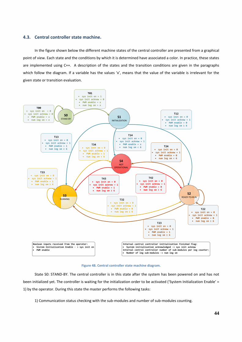
44
4.3. Central controller state machine.
In the figure shown below the different machine states of the central controller are presented from a graphical
point of view. Each state and the conditions by which it is determined have associated a color. In practice, these states
are implemented using C++. A description of the states and the transition conditions are given in the paragraphs
which follow the diagram. If a variable has the values ‘x’, means that the value of the variable is irrelevant for the
given state or transition evaluation.
S0STAND-BY
S1INITIALIZATION
S2READY-TO-RUN
T01 sys init en = 1
sys init acknow = 0 PWM enable = x num leg sm = x
T00 sys init en = 0
sys init acknow = 0 PWM enable = x num leg sm = x
T23 sys init en = 0
sys init acknow = 1 PWM enable = 1 num leg sm ≥ 6
T32 sys init en = 0
sys init acknow = 1 PWM enable = 0 num leg sm ≥ 6
S3RUNNING
T12 sys init en = 0
sys init acknow = 1 PWM enable = 0 num leg sm ≥ 6
Boolean inputs received from the operator: Sistem Initialization Enable - > sys init en PWM enable
Internal central controller initialization finished flag: System initialization acknowledged -> sys init acknowInternal central controller number of sub-modules per leg counter: Number of leg sub-modules -> num leg sm
T22 sys init en = 0
sys init acknow = 1 PWM enable = 0 num leg sm ≥ 6
T13 sys init en = 0
sys init acknow = 1 PWM enable = 1 num leg sm ≥ 6
T33 sys init en = 0
sys init acknow = 1 PWM enable = 1 num leg sm ≥ 6
S4NOT
OPERATIONAL
T24 sys init en = 0
sys init acknow = 1 PWM enable = 0 num leg sm < 6
T34 sys init en = 0
sys init acknow = 1 PWM enable = 1 num leg sm < 6
T42 sys init en = 0
sys init acknow = 1 PWM enable = 0 num leg sm ≥ 6
T43 sys init en = 0
sys init acknow = 1 PWM enable = 1 num leg sm ≥ 6
T14 sys init en = 0
sys init acknow = 1 PWM enable = x num leg sm < 6
Figure 48. Central controller state machine diagram.
State S0: STAND-BY. The central controller is in this state after the system has been powered on and has not
been initialized yet. The controller is waiting for the initialization order to be activated (‘System Initialization Enable’ =
1) by the operator. During this state the master performs the following tasks:
1) Communication status checking with the sub-modules and number of sub-modules counting.
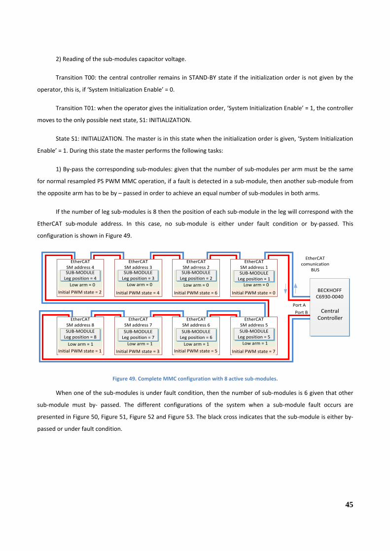
45
2) Reading of the sub-modules capacitor voltage.
Transition T00: the central controller remains in STAND-BY state if the initialization order is not given by the
operator, this is, if ‘System Initialization Enable’ = 0.
Transition T01: when the operator gives the initialization order, ‘System Initialization Enable’ = 1, the controller
moves to the only possible next state, S1: INITIALIZATION.
State S1: INITIALIZATION. The master is in this state when the initialization order is given, ‘System Initialization
Enable’ = 1. During this state the master performs the following tasks:
1) By-pass the corresponding sub-modules: given that the number of sub-modules per arm must be the same
for normal resampled PS PWM MMC operation, if a fault is detected in a sub-module, then another sub-module from
the opposite arm has to be by – passed in order to achieve an equal number of sub-modules in both arms.
If the number of leg sub-modules is 8 then the position of each sub-module in the leg will correspond with the
EtherCAT sub-module address. In this case, no sub-module is either under fault condition or by-passed. This
configuration is shown in Figure 49.
EtherCAT comunication
BUS
Port A
BECKHOFF C6930-0040
CentralController
Port B
EtherCAT SM address 4SUB-MODULE
Leg position = 4
EtherCAT SM address 3SUB-MODULE
Leg position = 3
EtherCAT SM adrress 2SUB-MODULE
Leg position = 2
EtherCAT SM address 1SUB-MODULE
Leg position = 1
EtherCAT SM address 8
SUB-MODULELeg position = 8
EtherCAT SM address 7
SUB-MODULELeg position = 7
EtherCAT SM address 6
SUB-MODULELeg position = 6
EtherCAT SM address 5
SUB-MODULELeg position = 5
Low arm = 0 Low arm = 0 Low arm = 0 Low arm = 0
Low arm = 1Low arm = 1Low arm = 1Low arm = 1
Initial PWM state = 2 Initial PWM state = 4 Initial PWM state = 6 Initial PWM state = 0
Initial PWM state = 1 Initial PWM state = 3 Initial PWM state = 5 Initial PWM state = 7
Figure 49. Complete MMC configuration with 8 active sub-modules.
When one of the sub-modules is under fault condition, then the number of sub-modules is 6 given that other
sub-module must by- passed. The different configurations of the system when a sub-module fault occurs are
presented in Figure 50, Figure 51, Figure 52 and Figure 53. The black cross indicates that the sub-module is either by-
passed or under fault condition.
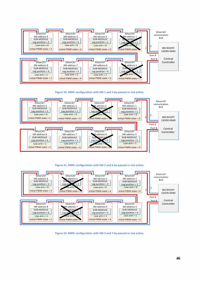
46
EtherCAT comunication
BUS
Port A
BECKHOFF C6930-0040
CentralController
Port B
EtherCAT SM address 4SUB-MODULE
Leg position = 3
EtherCAT SM address 3SUB-MODULE
Leg position = 2
EtherCAT SM adrress 2SUB-MODULE
Leg position = 1
EtherCAT SM address 1SUB-MODULE
Leg position = 1
EtherCAT SM address 8
SUB-MODULELeg position = 6
EtherCAT SM address 7
SUB-MODULELeg position = 5
EtherCAT SM address 6
SUB-MODULELeg position = 4
EtherCAT SM address 5
SUB-MODULELeg position = 5
Low arm = 0 Low arm = 0 Low arm = 0 Low arm = 0
Low arm = 1Low arm = 1Low arm = 1Low arm = 1
Initial PWM state = 2 Initial PWM state = 4 Initial PWM state = 0 Initial PWM state = 0
Initial PWM state = 2 Initial PWM state = 4 Initial PWM state = 0 Initial PWM state = 7
Figure 50. MMC configuration with SM 1 and 5 by-passed or not-active.
EtherCAT comunication
BUS
Port A
BECKHOFF C6930-0040
CentralController
Port B
EtherCAT SM address 4SUB-MODULE
Leg position = 3
EtherCAT SM address 3SUB-MODULE
Leg position = 2
EtherCAT SM adrress 2SUB-MODULE
Leg position = 1
EtherCAT SM address 1SUB-MODULE
Leg position = 1
EtherCAT SM address 8
SUB-MODULELeg position = 6
EtherCAT SM address 7
SUB-MODULELeg position = 5
EtherCAT SM address 6
SUB-MODULELeg position = 4
EtherCAT SM address 5
SUB-MODULELeg position = 4
Low arm = 0 Low arm = 0 Low arm = 0 Low arm = 0
Low arm = 1Low arm = 1Low arm = 1Low arm = 1
Initial PWM state = 2 Initial PWM state = 4 Initial PWM state = 0 Initial PWM state = 0
Initial PWM state = 2 Initial PWM state = 4 Initial PWM state = 0 Initial PWM state = 0
Figure 51. MMC configuration with SM 2 and 6 by-passed or not-active.
EtherCAT comunication
BUS
Port A
BECKHOFF C6930-0040
CentralController
Port B
EtherCAT SM address 4SUB-MODULE
Leg position = 3
EtherCAT SM address 3SUB-MODULE
Leg position = 2
EtherCAT SM adrress 2SUB-MODULE
Leg position = 2
EtherCAT SM address 1SUB-MODULE
Leg position = 1
EtherCAT SM address 8
SUB-MODULELeg position = 6
EtherCAT SM address 7
SUB-MODULELeg position = 5
EtherCAT SM address 6
SUB-MODULELeg position = 5
EtherCAT SM address 5
SUB-MODULELeg position = 4
Low arm = 0 Low arm = 0 Low arm = 0 Low arm = 0
Low arm = 1Low arm = 1Low arm = 1Low arm = 1
Initial PWM state = 2 Initial PWM state = 4 Initial PWM state = 4 Initial PWM state = 0
Initial PWM state = 2 Initial PWM state = 4 Initial PWM state = 4 Initial PWM state = 0
Figure 52. MMC configuration with SM 3 and 7 by-passed or not-active.
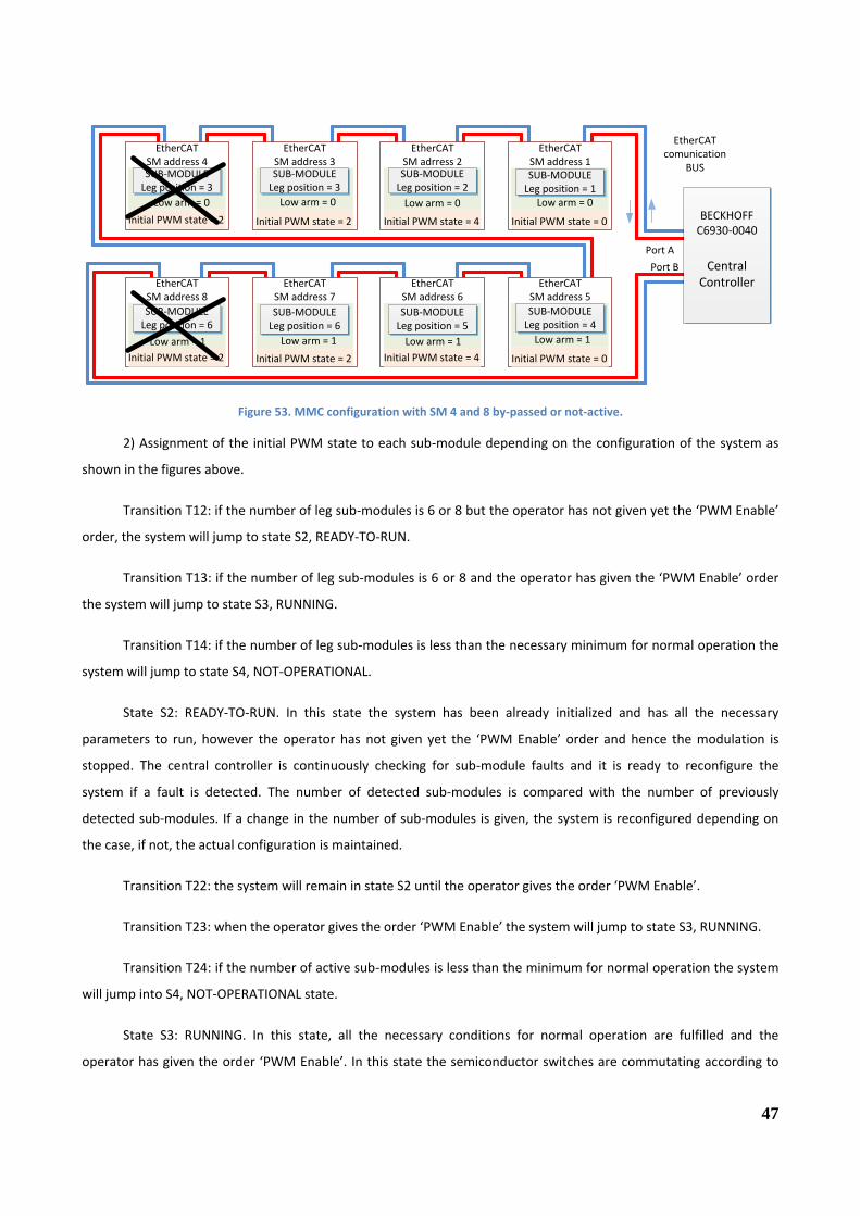
47
EtherCAT comunication
BUS
Port A
BECKHOFF C6930-0040
CentralController
Port B
EtherCAT SM address 4SUB-MODULE
Leg position = 3
EtherCAT SM address 3SUB-MODULE
Leg position = 3
EtherCAT SM adrress 2SUB-MODULE
Leg position = 2
EtherCAT SM address 1SUB-MODULE
Leg position = 1
EtherCAT SM address 8
SUB-MODULELeg position = 6
EtherCAT SM address 7
SUB-MODULELeg position = 6
EtherCAT SM address 6
SUB-MODULELeg position = 5
EtherCAT SM address 5
SUB-MODULELeg position = 4
Low arm = 0 Low arm = 0 Low arm = 0 Low arm = 0
Low arm = 1Low arm = 1Low arm = 1Low arm = 1
Initial PWM state = 2 Initial PWM state = 2 Initial PWM state = 4 Initial PWM state = 0
Initial PWM state = 2 Initial PWM state = 2 Initial PWM state = 4 Initial PWM state = 0
Figure 53. MMC configuration with SM 4 and 8 by-passed or not-active.
2) Assignment of the initial PWM state to each sub-module depending on the configuration of the system as
shown in the figures above.
Transition T12: if the number of leg sub-modules is 6 or 8 but the operator has not given yet the ‘PWM Enable’
order, the system will jump to state S2, READY-TO-RUN.
Transition T13: if the number of leg sub-modules is 6 or 8 and the operator has given the ‘PWM Enable’ order
the system will jump to state S3, RUNNING.
Transition T14: if the number of leg sub-modules is less than the necessary minimum for normal operation the
system will jump to state S4, NOT-OPERATIONAL.
State S2: READY-TO-RUN. In this state the system has been already initialized and has all the necessary
parameters to run, however the operator has not given yet the ‘PWM Enable’ order and hence the modulation is
stopped. The central controller is continuously checking for sub-module faults and it is ready to reconfigure the
system if a fault is detected. The number of detected sub-modules is compared with the number of previously
detected sub-modules. If a change in the number of sub-modules is given, the system is reconfigured depending on
the case, if not, the actual configuration is maintained.
Transition T22: the system will remain in state S2 until the operator gives the order ‘PWM Enable’.
Transition T23: when the operator gives the order ‘PWM Enable’ the system will jump to state S3, RUNNING.
Transition T24: if the number of active sub-modules is less than the minimum for normal operation the system
will jump into S4, NOT-OPERATIONAL state.
State S3: RUNNING. In this state, all the necessary conditions for normal operation are fulfilled and the
operator has given the order ‘PWM Enable’. In this state the semiconductor switches are commutating according to
48
the resampled PS PWM and the implemented control techniques. As in the previous state, the central controller is
continuously checking for sub-module faults. The number of detected sub-modules is compared with the number of
previously detected sub-modules. If a change in the number of sub-modules is encountered, the system is
reconfigured depending on the given case, if not, the actual configuration is maintained.
Transition T32: the system will jump to the READY-TO-RUN state when the operator stops the modulation,
‘PWM Enable’ = 0.
Transition T34: if the number of leg sub-modules is less than the necessary minimum for normal operation the
system will jump to state S4, NOT-OPERATIONAL.
State S4: NOT-OPERATIONAL. The system will stay in this state as long as the ‘System Initialization’ order has
been given by the operator and the detected number of leg sub-modules is less than 6.
Transition T42: if the detected number of leg sub-modules is 6 or 8 and the order ‘PWM Enable’ is not given by
the operator, the system will jump to READY-TO-RUN state.
Transition T43: if the detected number of leg sub-modules is 6 or 8 and the order ‘PWM Enable’ is given by the
operator, the system will jump to READY-TO-RUN state.
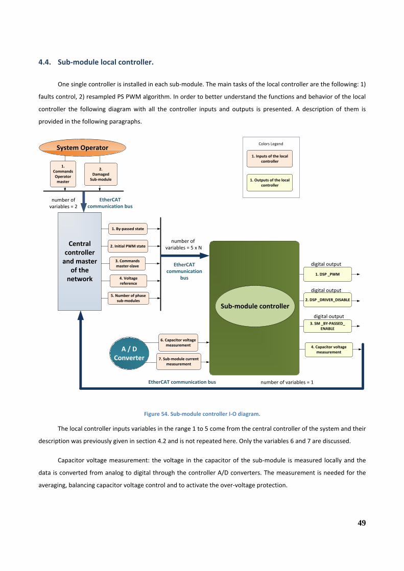
49
4.4. Sub-module local controller.
One single controller is installed in each sub-module. The main tasks of the local controller are the following: 1)
faults control, 2) resampled PS PWM algorithm. In order to better understand the functions and behavior of the local
controller the following diagram with all the controller inputs and outputs is presented. A description of them is
provided in the following paragraphs.
4. Capacitor voltage measurement
1.Commands Operator master
System Operator
2.Damaged
Sub-module
6. Capacitor voltage measurement
7. Sub-module current measurement
1. By-passed state
2. Initial PWM state
5. Number of phase sub-modules
4. Voltage reference
3. Commands master-slave
Central controller
and master of the
network
number of variables = 5 x N
number of variables = 1
number of variables = 2
EtherCAT communication bus
Sub-module controller
EtherCAT communication bus
A / DConverter
EtherCAT communication
bus
3. SM _BY-PASSED_ ENABLE
2. DSP _DRIVER_DISABLE
1. DSP _PWM
1. Inputs of the local controller
Colors Legend
1. Outputs of the local controller
digital output
digital output
digital output
Figure 54. Sub-module controller I-O diagram.
The local controller inputs variables in the range 1 to 5 come from the central controller of the system and their
description was previously given in section 4.2 and is not repeated here. Only the variables 6 and 7 are discussed.
Capacitor voltage measurement: the voltage in the capacitor of the sub-module is measured locally and the
data is converted from analog to digital through the controller A/D converters. The measurement is needed for the
averaging, balancing capacitor voltage control and to activate the over-voltage protection.
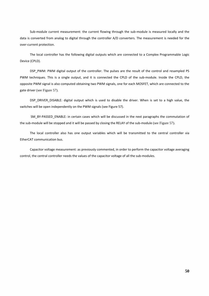
50
Sub-module current measurement: the current flowing through the sub-module is measured locally and the
data is converted from analog to digital through the controller A/D converters. The measurement is needed for the
over-current protection.
The local controller has the following digital outputs which are connected to a Complex Programmable Logic
Device (CPLD).
DSP_PWM: PWM digital output of the controller. The pulses are the result of the control and resampled PS
PWM techniques. This is a single output, and it is connected the CPLD of the sub-module. Inside the CPLD, the
opposite PWM signal is also computed obtaining two PWM signals, one for each MOSFET, which are connected to the
gate driver (see Figure 57).
DSP_DRIVER_DISABLE: digital output which is used to disable the driver. When is set to a high value, the
switches will be open independently on the PWM signals (see Figure 57).
SM_BY-PASSED_ENABLE: in certain cases which will be discussed in the next paragraphs the commutation of
the sub-module will be stopped and it will be passed by closing the RELAY of the sub-module (see Figure 57).
The local controller also has one output variables which will be transmitted to the central controller via
EtherCAT communication bus.
Capacitor voltage measurement: as previously commented, in order to perform the capacitor voltage averaging
control, the central controller needs the values of the capacitor voltage of all the sub-modules.
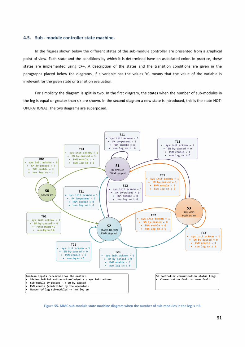
51
4.5. Sub - module controller state machine.
In the figures shown below the different states of the sub-module controller are presented from a graphical
point of view. Each state and the conditions by which it is determined have an associated color. In practice, these
states are implemented using C++. A description of the states and the transition conditions are given in the
paragraphs placed below the diagrams. If a variable has the values ‘x’, means that the value of the variable is
irrelevant for the given state or transition evaluation.
For simplicity the diagram is split in two. In the first diagram, the states when the number of sub-modules in
the leg is equal or greater than six are shown. In the second diagram a new state is introduced, this is the state NOT-
OPERATIONAL. The two diagrams are superposed.
S0STAND-BY
S2READY-TO-RUNPWM stopped
T02 sys init acknow = 1
SM by-passed = 0 PWM enable = 0 num leg sm ≥ 6
T00 sys init acknow = 0
SM by-passed = x PWM enable = x num leg sm = x
T12 sys init acknow = 1
SM by-passed = 0 PWM enable = 0 num leg sm ≥ 6
S1BY-PASSED
PWM stopped
T01 sys init acknow = 1
SM by-passed = 1 PWM enable = x num leg sm ≥ 6
T21 sys init acknow = 1
SM by-passed = 1 PWM enable = 0 num leg sm ≥ 6
T22 sys init acknow = 1
SM by-passed = 0 PWM enable = 0
num leg sm ≥ 6
T11 sys init acknow = 1
SM by-passed = 1 PWM enable = x
num leg sm ≥ 6
T13 sys init acknow = 1
SM by-passed = 0 PWM enable = 1 num leg sm ≥ 6
T31 sys init acknow = 1
SM by-passed = 1 PWM enable = 1 num leg sm ≥ 6
T23 sys init acknow = 1
SM by-passed = 0 PWM enable = 1 num leg sm ≥ 6
T33 sys init acknow = 1
SM by-passed = 0 PWM enable = 1 num leg sm ≥ 6
T32 sys init acknow = 1
SM by-passed = 0 PWM enable = 0 num leg sm ≥ 6
Boolean inputs received from the master: Sistem initialization acknowledged - > sys init acknow Sub-module by-passed - > SM by-passed PWM enable (controller by the operator) Number of leg sub-modules -> num leg sm
SM controller communication status flag: Communication fault -> comm fault
S3RUNNING
PWM active
Figure 55. MMC sub-module state machine diagram when the number of sub-modules in the leg is ≥ 6.
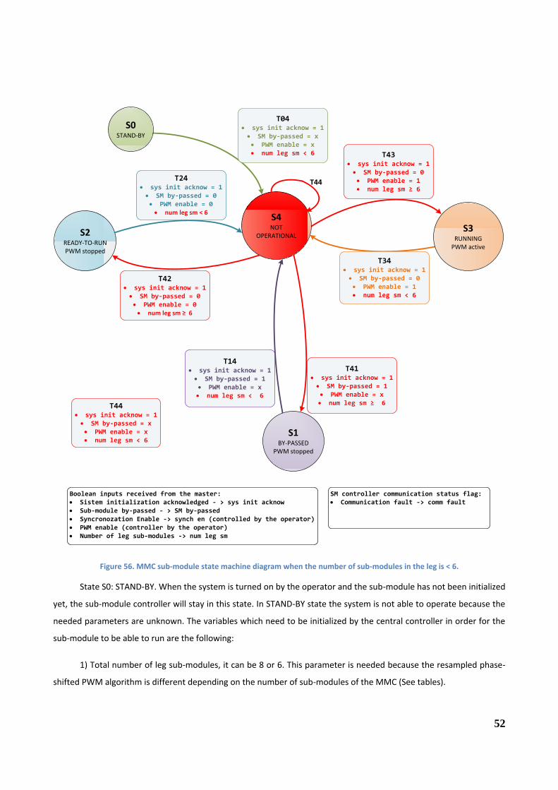
52
S0STAND-BY
S2READY-TO-RUNPWM stopped
S1BY-PASSED
PWM stopped
T04 sys init acknow = 1
SM by-passed = x PWM enable = x num leg sm < 6
T24 sys init acknow = 1
SM by-passed = 0 PWM enable = 0
num leg sm < 6
T14 sys init acknow = 1
SM by-passed = 1 PWM enable = x
num leg sm < 6
T34 sys init acknow = 1
SM by-passed = 0 PWM enable = 1 num leg sm < 6
Boolean inputs received from the master: Sistem initialization acknowledged - > sys init acknow Sub-module by-passed - > SM by-passed Syncronozation Enable -> synch en (controlled by the operator) PWM enable (controller by the operator) Number of leg sub-modules -> num leg sm
SM controller communication status flag: Communication fault -> comm fault
S3RUNNING
PWM active
S4NOT
OPERATIONAL
T43 sys init acknow = 1
SM by-passed = 0 PWM enable = 1 num leg sm ≥ 6
T42 sys init acknow = 1
SM by-passed = 0 PWM enable = 0
num leg sm ≥ 6
T41 sys init acknow = 1
SM by-passed = 1 PWM enable = x
num leg sm ≥ 6T44 sys init acknow = 1
SM by-passed = x PWM enable = x num leg sm < 6
T44
Figure 56. MMC sub-module state machine diagram when the number of sub-modules in the leg is < 6.
State S0: STAND-BY. When the system is turned on by the operator and the sub-module has not been initialized
yet, the sub-module controller will stay in this state. In STAND-BY state the system is not able to operate because the
needed parameters are unknown. The variables which need to be initialized by the central controller in order for the
sub-module to be able to run are the following:
1) Total number of leg sub-modules, it can be 8 or 6. This parameter is needed because the resampled phase-
shifted PWM algorithm is different depending on the number of sub-modules of the MMC (See tables).
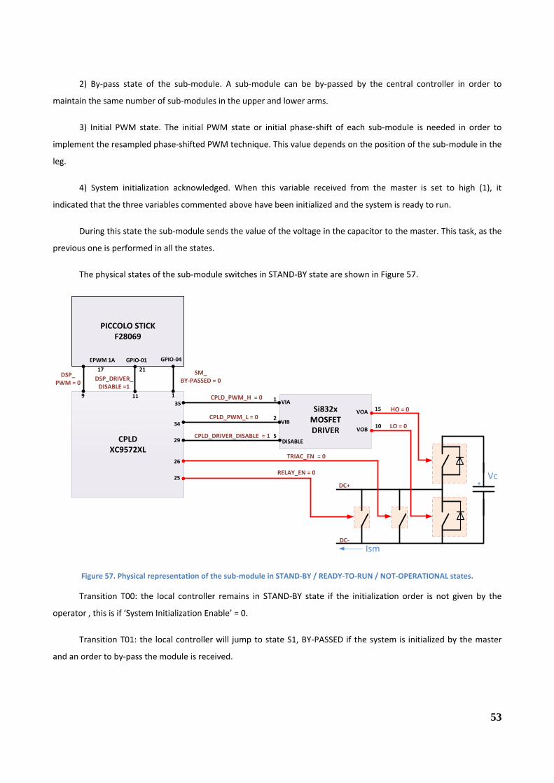
53
2) By-pass state of the sub-module. A sub-module can be by-passed by the central controller in order to
maintain the same number of sub-modules in the upper and lower arms.
3) Initial PWM state. The initial PWM state or initial phase-shift of each sub-module is needed in order to
implement the resampled phase-shifted PWM technique. This value depends on the position of the sub-module in the
leg.
4) System initialization acknowledged. When this variable received from the master is set to high (1), it
indicated that the three variables commented above have been initialized and the system is ready to run.
During this state the sub-module sends the value of the voltage in the capacitor to the master. This task, as the
previous one is performed in all the states.
The physical states of the sub-module switches in STAND-BY state are shown in Figure 57.
CPLD XC9572XL
Si832xMOSFET DRIVER
VIA
VIB
DISABLE
1
2
5
15
10
VOA
VOB
CPLD_PWM_H = 0
CPLD_PWM_L = 0
CPLD_DRIVER_DISABLE = 1
HO = 0
LO = 0
PICCOLO STICKF28069
DSP_PWM = 0
DSP_DRIVER_DISABLE =1
29
34
35
9 11
17 21
GPIO-01EPWM 1A
TRIAC_EN = 026
RELAY_EN = 025
DC+
DC-
Ism
Vc+
GPIO-04
SM_BY-PASSED = 0
1
Figure 57. Physical representation of the sub-module in STAND-BY / READY-TO-RUN / NOT-OPERATIONAL states.
Transition T00: the local controller remains in STAND-BY state if the initialization order is not given by the
operator , this is if ‘System Initialization Enable’ = 0.
Transition T01: the local controller will jump to state S1, BY-PASSED if the system is initialized by the master
and an order to by-pass the module is received.
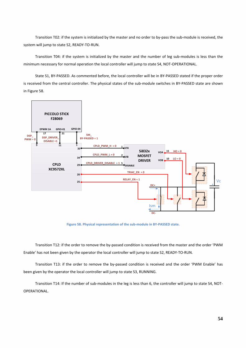
54
Transition T02: if the system is initialized by the master and no order to by-pass the sub-module is received, the
system will jump to state S2, READY-TO-RUN.
Transition T04: if the system is initialized by the master and the number of leg sub-modules is less than the
minimum necessary for normal operation the local controller will jump to state S4, NOT-OPERATIONAL.
State S1, BY-PASSED. As commented before, the local controller will be in BY-PASSED stated if the proper order
is received from the central controller. The physical states of the sub-module switches in BY-PASSED state are shown
in Figure 58.
CPLD XC9572XL
Si832xMOSFET DRIVER
VIA
VIB
DISABLE
1
2
5
15
10
VOA
VOB
CPLD_PWM_H = 0
CPLD_PWM_L = 0
CPLD_DRIVER_DISABLE = 1
HO = 0
LO = 0
PICCOLO STICKF28069
DSP_PWM = 0
DSP_DRIVER_DISABLE =1
29
34
35
9 11
17 21
GPIO-01EPWM 1A
TRIAC_EN = 026
RELAY_EN = 125
DC+
DC-
Ism
Vc+
GPIO-04
SM_BY-PASSED = 1
1
Figure 58. Physical representation of the sub-module in BY-PASSED state.
Transition T12: if the order to remove the by-passed condition is received from the master and the order ‘PWM
Enable’ has not been given by the operator the local controller will jump to state S2, READY-TO-RUN.
Transition T13: if the order to remove the by-passed condition is received and the order ‘PWM Enable’ has
been given by the operator the local controller will jump to state S3, RUNNING.
Transition T14: If the number of sub-modules in the leg is less than 6, the controller will jump to state S4, NOT-
OPERATIONAL.
55
State S2, READY-TO-RUN. The sub-module controller has received all the needed parameters in order to start
normal operation, however, the operator has not given the starting order ‘PWM Enable’ yet. The states of the
different switches of the sub-module are the same as in STAND-BY state and can be seen in Figure 57.
Transition T21: if the proper order is received from the master the local controller will jump to state S1, BY-
PASSED.
Transition T22: the local controller will remain in state S2, READY-TO-RUN if the running order is not given by
the operator.
Transition T23: if the operator gives the running order, ´PWM Enable = 1´, the sub-module controller will jump
to state S3, RUNNING.
Transition T24: in case the number of sub-modules per leg is less than the minimum necessary for normal
operation the sub-module will jump to state S4, NOT-OPERATIONAL.
State S3: RUNNING. In this state the operator has given the order to run the system, ‘PWM Enable’ = 1. The
converter is working in normal conditions, the reference is received from the master and the different control and
resampled PS PWM algorithms are computed.
Transition T31: if the proper order is received from the master the local controller will jump to state S1, BY-
PASSED.
Transition T32: if the operator gives the order to stop the modulation, ´PWM Enable = 0´, the local controller
will jump to state S2, READY-TO-RUN.
Transition T33: the controller will remain in state S3, RUNNING, if no different order is given from the operator
or fault occurs.
Transition T34: if a fault occurs and the number of sub-modules in the leg is less the six, the sub-module
controller will jump to state S4, NOT-OPERATIONAL.
State S4, NOT-OPERATIONAL: the local controller will remain in this state as long as the number of sub-modules
in the leg is less than the minimum necessary for normal operation. . The states of the different switches of the sub-
module are the same as in STAND-BY state and can be seen in Figure 57.
Transition T41: if the number of sub-modules per leg is 6 or 8 and the by-pass order is received from the master
the local controller will jump to state S1, BY-PASSED.
Transition T42: if the number of sub-modules per leg is 6 or 8 and no order to run has been given by the
operator the local controller will jump to state S1, READY-TO-RUN.

56
Transition T43: if the number of sub-modules per leg is 6 and 8 and the operator has given the order to run the
system, the local controller will jump to state S3, RUNNING.
Transition T44: while the number of leg sub-modules is less than 6, the controller will remain in state S4, NOT-
OPERATIONAL.
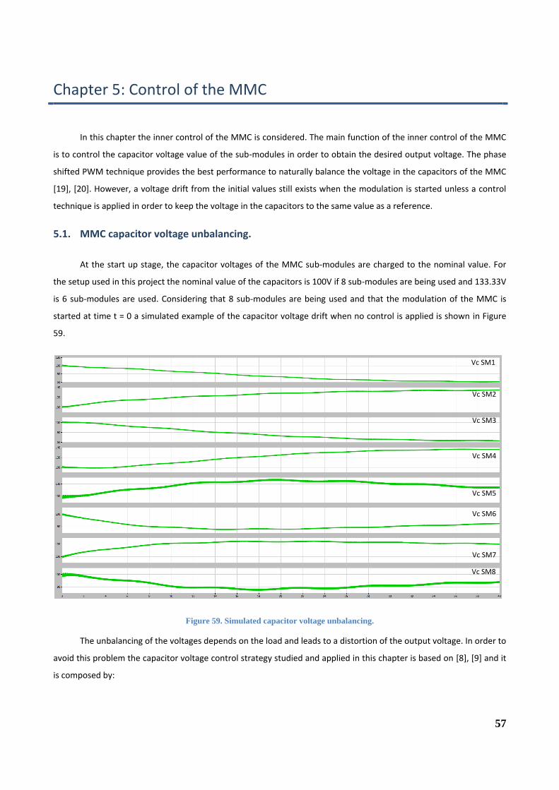
57
Chapter 5: Control of the MMC
In this chapter the inner control of the MMC is considered. The main function of the inner control of the MMC
is to control the capacitor voltage value of the sub-modules in order to obtain the desired output voltage. The phase
shifted PWM technique provides the best performance to naturally balance the voltage in the capacitors of the MMC
[19], [20]. However, a voltage drift from the initial values still exists when the modulation is started unless a control
technique is applied in order to keep the voltage in the capacitors to the same value as a reference.
5.1. MMC capacitor voltage unbalancing.
At the start up stage, the capacitor voltages of the MMC sub-modules are charged to the nominal value. For
the setup used in this project the nominal value of the capacitors is 100V if 8 sub-modules are being used and 133.33V
is 6 sub-modules are used. Considering that 8 sub-modules are being used and that the modulation of the MMC is
started at time t = 0 a simulated example of the capacitor voltage drift when no control is applied is shown in Figure
59.
Vc SM1
Vc SM2
Vc SM3
Vc SM4
Vc SM5
Vc SM6
Vc SM7
Vc SM8
Figure 59. Simulated capacitor voltage unbalancing.
The unbalancing of the voltages depends on the load and leads to a distortion of the output voltage. In order to
avoid this problem the capacitor voltage control strategy studied and applied in this chapter is based on [8], [9] and it
is composed by:
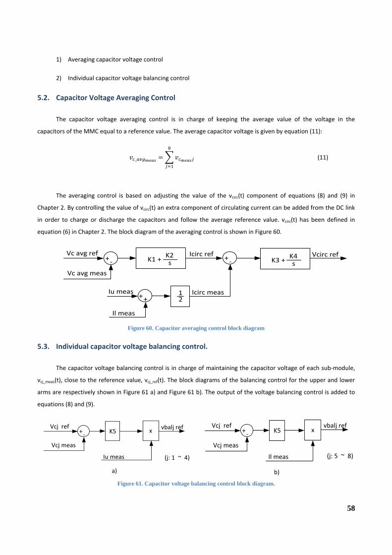
58
1) Averaging capacitor voltage control
2) Individual capacitor voltage balancing control
5.2. Capacitor Voltage Averaging Control
The capacitor voltage averaging control is in charge of keeping the average value of the voltage in the
capacitors of the MMC equal to a reference value. The average capacitor voltage is given by equation (11):
∑
(11)
The averaging control is based on adjusting the value of the vcirc(t) component of equations (8) and (9) in
Chapter 2. By controlling the value of vcirc(t) an extra component of circulating current can be added from the DC link
in order to charge or discharge the capacitors and follow the average reference value. vcirc(t) has been defined in
equation (6) in Chapter 2. The block diagram of the averaging control is shown in Figure 60.
+-+- K1 +K2s K3 +
K4s
+ 12
Vc avg ref
Vc avg meas
Iu meas
Il meas
Icirc meas
Icirc ref Vcirc ref
+
Figure 60. Capacitor averaging control block diagram
5.3. Individual capacitor voltage balancing control.
The capacitor voltage balancing control is in charge of maintaining the capacitor voltage of each sub-module,
vcj_meas(t), close to the reference value, vcj_ref(t). The block diagrams of the balancing control for the upper and lower
arms are respectively shown in Figure 61 a) and Figure 61 b). The output of the voltage balancing control is added to
equations (8) and (9).
+- K5 xVcj ref
Vcj meas
Iu meas
vbalj ref
(j: 1 ~ 4)
a)
+- K5 xVcj ref
Vcj meas
Il meas
vbalj ref
(j: 5 ~ 8)
b)
Figure 61. Capacitor voltage balancing control block diagram.
59
Two models of the MMC have been built using PLEX in order to simulate the commented control strategies
before its implementation in the real setup. The first model has been built using eight sub-modules per phase and the
second one using six. The model with eight sub-modules simulates the MMC behavior under normal operation and
the model with six sub-modules simulates the behavior of the system after a fault reconfiguration.
5.4. Simulation results 8 sub-module MMC.
Taking into account that the capacitor voltage of the sub-modules must be kept equal to Vc = E /4, the upper
and lower arm reference equations for each sub-module are the following
( ) ( ) ( )
( )
( ) ( ) ( )
( )
( ) ( ) ( )
( )
( ) ( ) ( )
( )
( ) ( ) ( )
( )
( ) ( ) ( )
( )
( ) ( ) ( )
( )
( ) ( ) ( )
( )
If the capacitor voltage of all sub-modules is kept equal to Vc = 2E /N by then control algorithm, where N is
equal to 8, then:
( ) ( ) ( )
( )
( ) ( ) ( )
( )
( ) ( ) ( )
( )
( ) ( ) ( )
( )
( ) ( ) ( )
( )
( ) ( ) ( )
( )
( ) ( ) ( )
( )
( ) ( ) ( )
( )
60
The voltage commands of each sub-module are normalized by each capacitor voltage value and then compared
with a triangular wave with a maximum and minimum value of 1 and 0 respectively and a frequency fcar. As a result of
this a nine level output voltage is obtained with an equivalent switching frequency of 8*fcar. The circuit parameters
and control gains used for the simulations are presented below:
DC supply voltage ±200V
Number of sub-modules 8
Sub-module capacitor value 6mF
Nominal capacitor voltage 100V
Arm resistance 0.01Ω
Arm inductance 1.8e-2H
Load resistance 35Ω
Load inductance 6.8mH
Carrier frequency 250Hzh
Equivalent switching frequency 250Hz *8 = 2kHz
Sampling frequency 2kHz
K1 10
K2 100
K3 10
K4 140
K5 0.4
In the figures presented below some simulated waves are shown. In Figure 62 the behavior of the capacitor
voltage is presented. In this case the reference for the capacitor voltages is kept constant to a value of 100V. As can be
observed the reference is being correctly followed and no voltage drift if present. A zoom of capacitor voltage waves is
given in Figure 63.
In order to test the performance of the control a voltage step is applied as a capacitor voltage reference in
Figure 65. At the bottom of the figure, the red line is the capacitor voltage reference and the blue line is the measured
capacitor voltage. As can be seen the behavior of the system is satisfactory and the reference is followed by the
system. The output voltage and current of the system with eight sub-modules are presented in Figure 65.
61
Vc SM1
Vc SM2
Vc SM3
Vc SM4
Vc SM5
Vc SM6
Vc SM7
Vc SM8
Vc average
Figure 62. Simulated capacitor voltage with averaging and balancing control and a constant voltage reference.
Vc SM1
Vc SM2
Vc SM3
Vc SM4
Vc SM5
Vc SM6
Vc SM7
Vc SM8
Vc average
Figure 63. . Simulated capacitor voltage with averaging and balancing control and a constant voltage reference.
62
Vc SM1
Vc SM2
Vc SM3
Vc SM4
Vc SM5
Vc SM6
Vc SM7
Vc SM8
Vc average
Figure 64. . Simulated capacitor voltage with averaging and balancing control and a step voltage reference.
Figure 65. Simulated output voltage and output current.
63
5.5. Simulation results 6 sub-module MMC.
In the case of the MMC with six sub-modules the capacitor voltages must be kept equal to Vc = E /3, the
command voltage equations are the following:
( ) ( ) ( )
( )
( ) ( ) ( )
( )
( ) ( ) ( )
( )
( ) ( ) ( )
( )
( ) ( ) ( )
( )
( ) ( ) ( )
( )
As a result of this a seven level output voltage is obtained with an equivalent switching frequency of 6*fcar. The
circuit parameters and control gains used for the simulations are presented below:
DC supply voltage ±200V
Number of sub-modules 6
Sub-module capacitor value 6mF
Nominal capacitor voltage 100V
Arm resistance 0.01Ω
Arm inductance 1.8e-2H
Load resistance 35Ω
Load inductance 6.8mH
Carrier frequency 333.33Hzh
Equivalent switching frequency 333.33*6 = 2kHz
Sampling frequency 2kHz
K1 10
K2 100
K3 3
K4 60
K5 0.3
64
In the figures presented below some simulated waves are shown. In Figure 66 the behavior of the capacitor
voltage is presented. In this case the reference for the capacitor voltages is kept constant to a value of 133.33V. As can
be observed the reference is being correctly followed and no voltage drift if present. A zoom of capacitor voltage
waves is given in Figure 67.
In order to test the performance of the control a voltage step is applied as a capacitor voltage reference in
Figure 68. At the bottom of the figure, the red line is the capacitor voltage reference and the blue line is the measured
capacitor voltage. As can be seen the behavior of the system is satisfactory and the reference is followed by the
system. The output voltage and current of the system with six sub-modules are presented in Figure 69.
Figure 66. Simulated capacitor voltage with averaging and balancing control and a constant voltage reference.
65
Vc SM1
Vc SM2
Vc SM3
Vc SM4
Vc SM5
Vc SM6
Vc average
Figure 67. Simulated capacitor voltage with averaging and balancing control and a constant voltage reference.
Vc SM1
Vc SM2
Vc SM3
Vc SM4
Vc SM5
Vc SM6
Vc average
Figure 68. Simulated capacitor voltage with averaging and balancing control and a step voltage reference.
66
Figure 69. Simulated output voltage and output current.
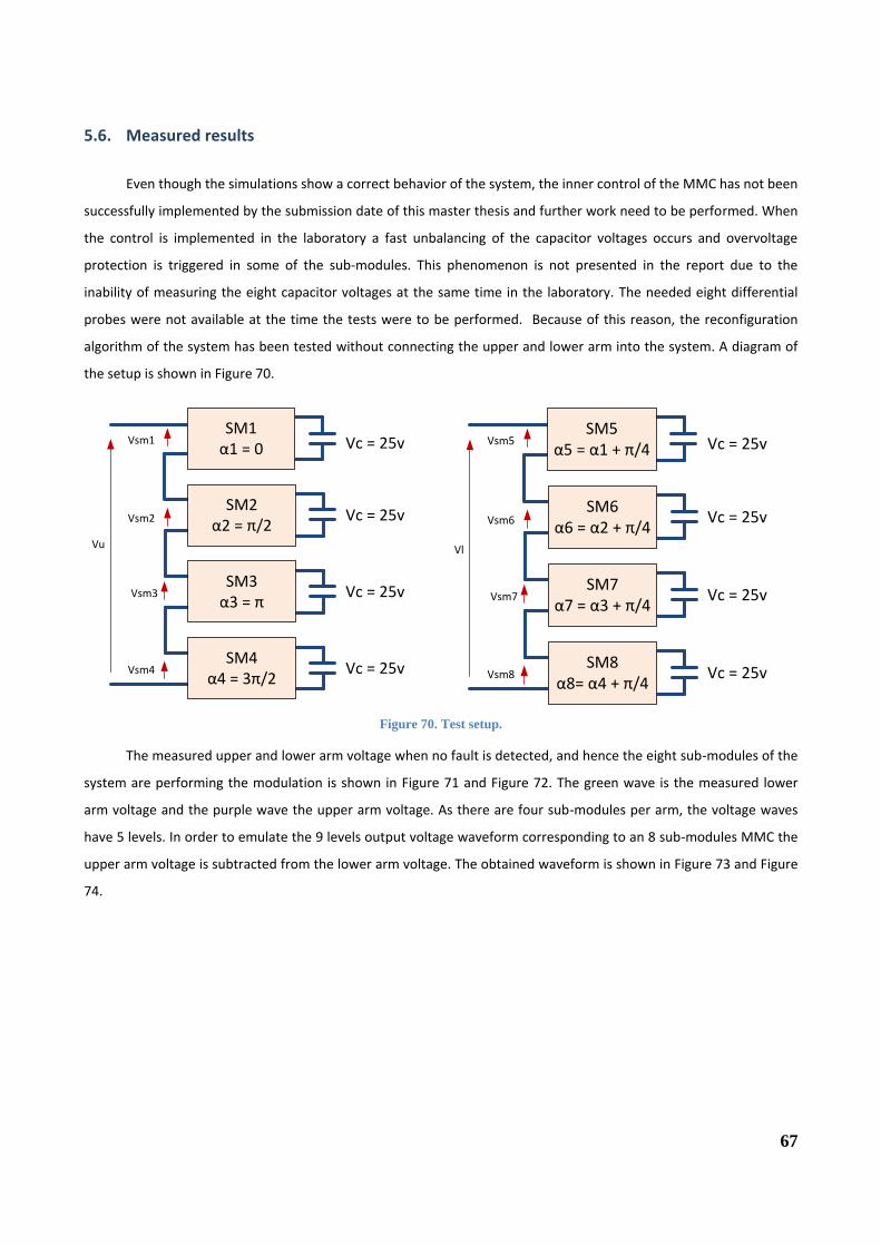
67
5.6. Measured results
Even though the simulations show a correct behavior of the system, the inner control of the MMC has not been
successfully implemented by the submission date of this master thesis and further work need to be performed. When
the control is implemented in the laboratory a fast unbalancing of the capacitor voltages occurs and overvoltage
protection is triggered in some of the sub-modules. This phenomenon is not presented in the report due to the
inability of measuring the eight capacitor voltages at the same time in the laboratory. The needed eight differential
probes were not available at the time the tests were to be performed. Because of this reason, the reconfiguration
algorithm of the system has been tested without connecting the upper and lower arm into the system. A diagram of
the setup is shown in Figure 70.
SM1α1 = 0 Vc = 25v
SM2α2 = π/2
SM3α3 = π
SM4α4 = 3π/2
Vsm1
Vsm2
Vsm3
Vsm4
Vu
Vc = 25v
Vc = 25v
Vc = 25v
SM5α5 = α1 + π/4 Vc = 25v
SM6α6 = α2 + π/4
SM7α7 = α3 + π/4
SM8α8= α4 + π/4
Vsm5
Vsm6
Vsm7
Vsm8
Vl
Vc = 25v
Vc = 25v
Vc = 25v
Figure 70. Test setup.
The measured upper and lower arm voltage when no fault is detected, and hence the eight sub-modules of the
system are performing the modulation is shown in Figure 71 and Figure 72. The green wave is the measured lower
arm voltage and the purple wave the upper arm voltage. As there are four sub-modules per arm, the voltage waves
have 5 levels. In order to emulate the 9 levels output voltage waveform corresponding to an 8 sub-modules MMC the
upper arm voltage is subtracted from the lower arm voltage. The obtained waveform is shown in Figure 73 and Figure
74.
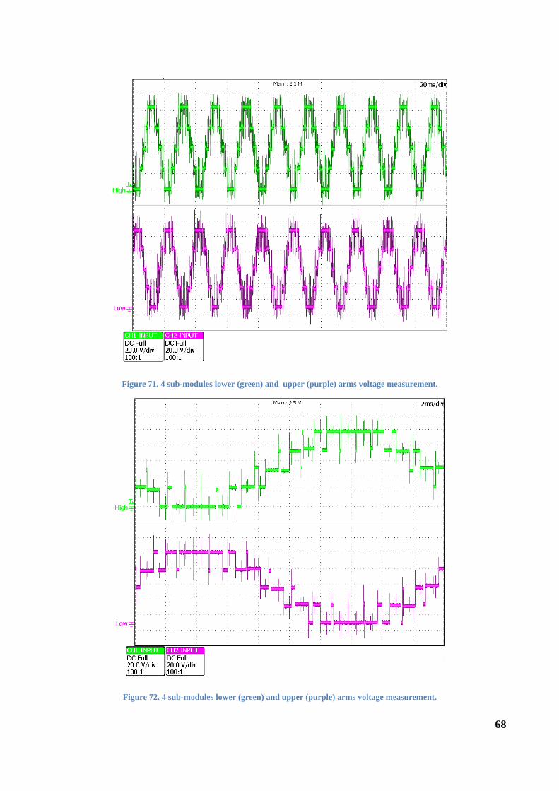
68
Figure 71. 4 sub-modules lower (green) and upper (purple) arms voltage measurement.
Figure 72. 4 sub-modules lower (green) and upper (purple) arms voltage measurement.
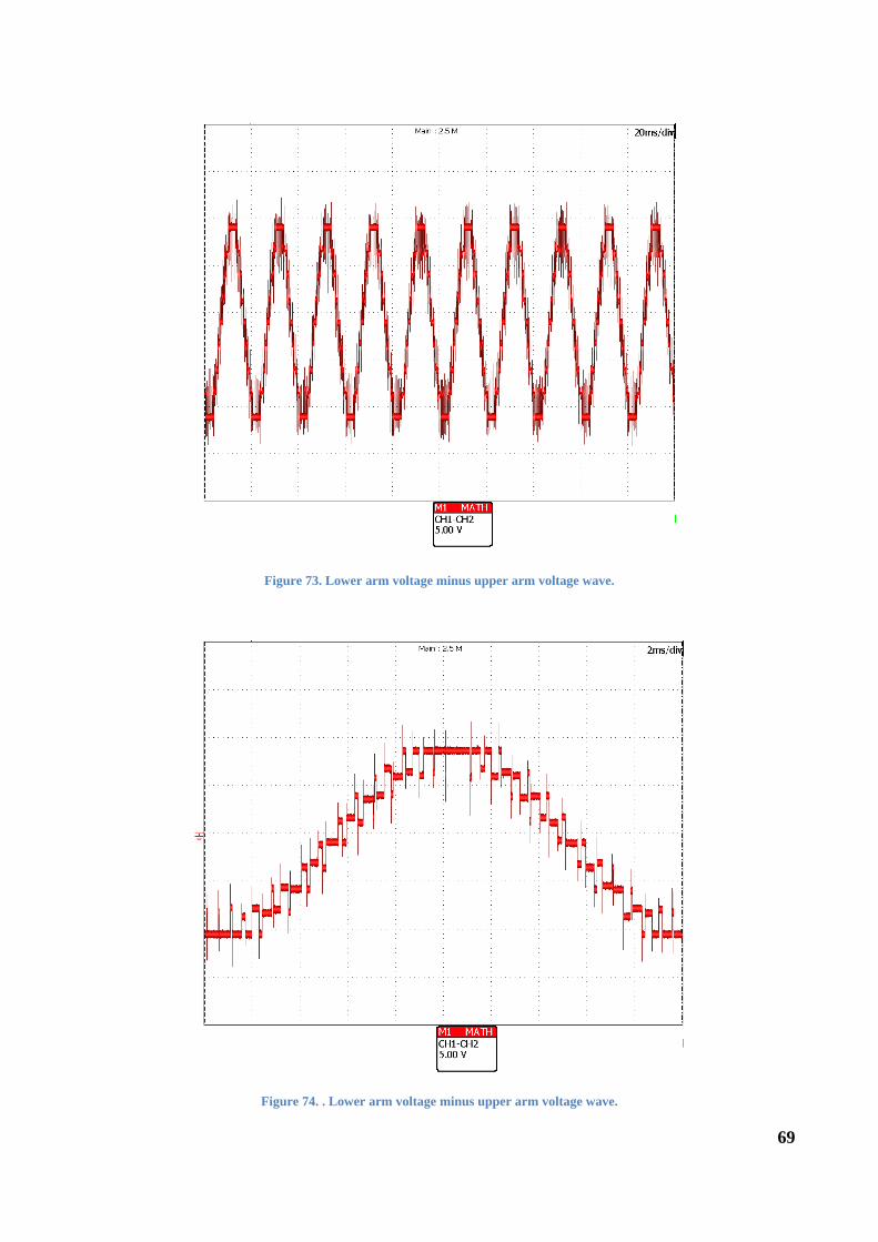
69
Figure 73. Lower arm voltage minus upper arm voltage wave.
Figure 74. . Lower arm voltage minus upper arm voltage wave.
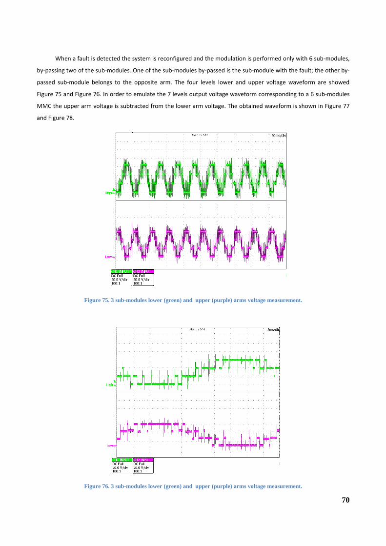
70
When a fault is detected the system is reconfigured and the modulation is performed only with 6 sub-modules,
by-passing two of the sub-modules. One of the sub-modules by-passed is the sub-module with the fault; the other by-
passed sub-module belongs to the opposite arm. The four levels lower and upper voltage waveform are showed
Figure 75 and Figure 76. In order to emulate the 7 levels output voltage waveform corresponding to a 6 sub-modules
MMC the upper arm voltage is subtracted from the lower arm voltage. The obtained waveform is shown in Figure 77
and Figure 78.
Figure 75. 3 sub-modules lower (green) and upper (purple) arms voltage measurement.
Figure 76. 3 sub-modules lower (green) and upper (purple) arms voltage measurement.
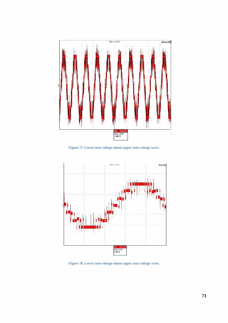
71
Figure 77. Lower arm voltage minus upper arm voltage wave.
Figure 78. Lower arm voltage minus upper arm voltage wave.

72
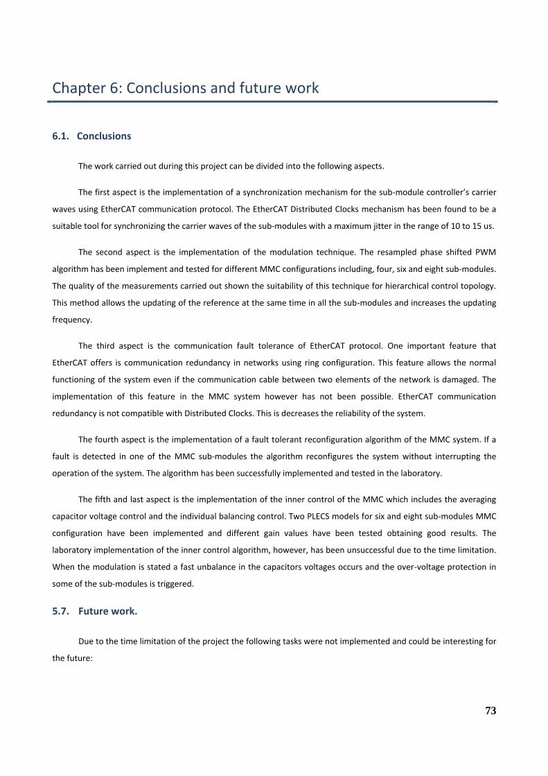
73
Chapter 6: Conclusions and future work
6.1. Conclusions
The work carried out during this project can be divided into the following aspects.
The first aspect is the implementation of a synchronization mechanism for the sub-module controller’s carrier
waves using EtherCAT communication protocol. The EtherCAT Distributed Clocks mechanism has been found to be a
suitable tool for synchronizing the carrier waves of the sub-modules with a maximum jitter in the range of 10 to 15 us.
The second aspect is the implementation of the modulation technique. The resampled phase shifted PWM
algorithm has been implement and tested for different MMC configurations including, four, six and eight sub-modules.
The quality of the measurements carried out shown the suitability of this technique for hierarchical control topology.
This method allows the updating of the reference at the same time in all the sub-modules and increases the updating
frequency.
The third aspect is the communication fault tolerance of EtherCAT protocol. One important feature that
EtherCAT offers is communication redundancy in networks using ring configuration. This feature allows the normal
functioning of the system even if the communication cable between two elements of the network is damaged. The
implementation of this feature in the MMC system however has not been possible. EtherCAT communication
redundancy is not compatible with Distributed Clocks. This is decreases the reliability of the system.
The fourth aspect is the implementation of a fault tolerant reconfiguration algorithm of the MMC system. If a
fault is detected in one of the MMC sub-modules the algorithm reconfigures the system without interrupting the
operation of the system. The algorithm has been successfully implemented and tested in the laboratory.
The fifth and last aspect is the implementation of the inner control of the MMC which includes the averaging
capacitor voltage control and the individual balancing control. Two PLECS models for six and eight sub-modules MMC
configuration have been implemented and different gain values have been tested obtaining good results. The
laboratory implementation of the inner control algorithm, however, has been unsuccessful due to the time limitation.
When the modulation is stated a fast unbalance in the capacitors voltages occurs and the over-voltage protection in
some of the sub-modules is triggered.
5.7. Future work.
Due to the time limitation of the project the following tasks were not implemented and could be interesting for
the future:
74
Finishing the implementation of the control strategy. The MMC cannot run without the averaging and
balancing control strategy properly implemented. This is the most fundamental task to be implemented in the future.
Communication speed limit. So far the minimum tested stable cycle time is 500us. The cycle time limits the
performance of the system and its reduction suppose an increase in the sampling and switching frequencies.
Reconfiguration when two sub-modules are under fault condition. In this project an algorithm which
reconfigures the system when one sub-module is under fault condition has been created. The improvement of this
algorithm in order to reconfigure the system when two sub-modules are under fault condition will improve the
reliability of the system even further.
In order to increase the usability and comfort when using the system the development of a user interface for
the operator of the system should be considered.
75
References
1. SIEMENS. (2011). High Voltage Direct Current Transmission - Proven Technology for Power Exchange [Online].
available: http://www.energy.siemens.com/hq/en/power-transmission/hvdc/.
2. ABB. (2013). HVDC Light - It's time to connect [Online]. available: http://new.abb.com/systems/hvdc/hvdc-light.
3. ABB. (2014, 10th April 2014). Introducing HVDC [Online]. available: http://new.abb.com/systems/hvdc/hvdc-light.
4. SIEMENS. (2009, 10th - April 2014). HVDC PLUS - Basics and Principle of Operation [Online]. available:
http://www.energy.siemens.com/hq/en/power-transmission/hvdc/hvdc-plus/.
5. ALSTOM. (2011, 10th - April 2012). HVDC - VSC : transmission technology of the future - Think Grid n.8 [Online].
available: http://www.alstom.com/grid/products-and-services/engineered-energy-solutions/hvdc-transmission-
systems/HVDC-MaxSine/.
6. ALSTOM. (2010). Voltage sourse converter - Introduction to VSC technology. [Online]. available:
http://www.alstom.com/grid/products-and-services/engineered-energy-solutions/hvdc-transmission-
systems/HVDC-MaxSine/.
7. S. Allebrod, R. Hamerski and R. Marquardt, "New transformerless, scalable Modular Multilevel Converters for
HVDC-transmission," in Power Electronics Specialists Conference, 2008. PESC 2008. IEEE, 2008, pp. 174-179.
8. M. Hagiwara and H. Akagi, "Control and experiment of pulsewidth-modulated modular multilevel converters,"
Power Electronics, IEEE Transactions on, vol. 24, no. 7, pp. 1737-1746 2009.
9. M. Hagiwara and H. Akagi, "PWM control and experiment of modular multilevel converters," in Power Electronics
Specialists Conference, 2008. PESC 2008. IEEE, 2008, pp. 154-161.
10. U.N. Gnanarathna, S.K. Chaudhary, A.M. Gole and R. Teodorescu, "Modular multi-level converter based HVDC
system for grid connection of offshore wind power plant," in AC and DC Power Transmission, 2010. ACDC. 9th
IET International Conference on, 2010, pp. 1-5.
11. ABB HVDC , T. Jonsson P. Lundberg S. Maiti Y. Jiang-Häfner. Converter Technologies and Functional
Requirements for Reliable and Economical HVDC Grid Design [Online]. available:
http://new.abb.com/systems/hvdc/hvdc-light.
12. ABB, Alireza Nami, Liwei Wang, Frans Dijkhuizen. Five level cross connected cell for cascaded
converters [Online]. available: http://new.abb.com/systems/hvdc/hvdc-light.
13. ABB, Jiaqi Liang*, Alireza Nami, Frans Dijkhuizen. Current Source Modular Multilevel Converter for HVDC and
FACTS [Online]. available: http://new.abb.com/systems/hvdc/hvdc-light.
14. C.C. Davidson and D.R. Trainer, "Innovative concepts for hybrid multi-level converters for HVDC power
transmission," in AC and DC Power Transmission, 2010. ACDC. 9th IET International Conference on, 2010, pp.
1-5.
15. SIEMENS. HVDC PLUS References [Online]. available: http://www.energy.siemens.com/hq/en/power-
transmission/hvdc/hvdc-plus/references.htm.
16. ABB. ABB Light References [Online]. available: http://new.abb.com/systems/hvdc/hvdc-light.
76
17. Young-Min Park, Han-Seong Yoo, Hyun-Won Lee, Myung-Gil Jung, Se-Hyun Lee, Choong-Dong Lee, Sang-Bin
Lee and Ji-Yoon Yoo, "A Simple and Reliable PWM Synchronization & Phase-Shift Method for Cascaded H-
Bridge Multilevel Inverters based on a Standard Serial Communication Protocol," in Industry Applications
Conference, 2006. 41st IAS Annual Meeting. Conference Record of the 2006 IEEE, 2006, pp. 988-994.
18. G.S. Konstantinou and V.G. Agelidis, "Performance evaluation of half-bridge cascaded multilevel converters
operated with multicarrier sinusoidal PWM techniques," in Industrial Electronics and Applications, 2009. ICIEA
2009. 4th IEEE Conference on, 2009, pp. 3399-3404.
19. Shaojun Huang, "Distributed modulation and control of modular multilevel converter for HVDC application<br />-
department of energy technology, aalborg university," 2013.
20. Juan Colmenares, "Analysis, implementation and experimental evaluation of a phase shifted PWM control system
for a modular multilevel converter<br />- KTH school of electrical engineering," 2011.
21. E. Petre Eni, "Fault tolerant distributed control strategy for modular multilevel converter in HVDC application -
department of energy technology, aalborg university," 2013.
22. Bechhoff, "Hardware data sheet ET1100," 2010.
23. G. Cena, I.C. Bertolotti, S. Scanzio, A. Valenzano and C. Zunino, "On the accuracy of the distributed clock
mechanism in EtherCAT," in Factory Communication Systems (WFCS), 2010 8th IEEE International Workshop
on, 2010, pp. 43-52.
24. Texas Instruments, "TMS320x2806x piccolo technical reference manual," 2011.

77
Appendix: OPTIM Conference 2014 Paper
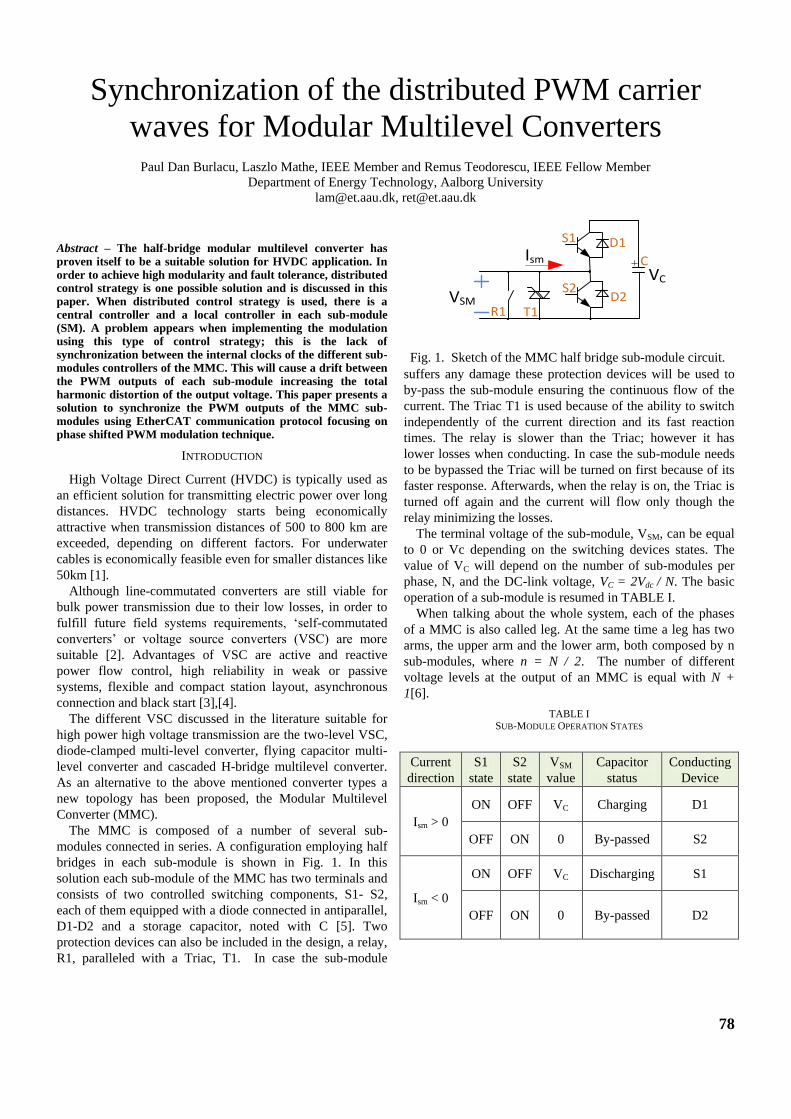
78
Synchronization of the distributed PWM carrier
waves for Modular Multilevel Converters
Paul Dan Burlacu, Laszlo Mathe, IEEE Member and Remus Teodorescu, IEEE Fellow Member
Department of Energy Technology, Aalborg University
[email protected], [email protected]
Abstract – The half-bridge modular multilevel converter has proven itself to be a suitable solution for HVDC application. In order to achieve high modularity and fault tolerance, distributed control strategy is one possible solution and is discussed in this paper. When distributed control strategy is used, there is a central controller and a local controller in each sub-module (SM). A problem appears when implementing the modulation using this type of control strategy; this is the lack of synchronization between the internal clocks of the different sub-modules controllers of the MMC. This will cause a drift between the PWM outputs of each sub-module increasing the total harmonic distortion of the output voltage. This paper presents a solution to synchronize the PWM outputs of the MMC sub-modules using EtherCAT communication protocol focusing on phase shifted PWM modulation technique.
INTRODUCTION
High Voltage Direct Current (HVDC) is typically used as
an efficient solution for transmitting electric power over long
distances. HVDC technology starts being economically
attractive when transmission distances of 500 to 800 km are
exceeded, depending on different factors. For underwater
cables is economically feasible even for smaller distances like
50km [1].
Although line-commutated converters are still viable for
bulk power transmission due to their low losses, in order to
fulfill future field systems requirements, ‘self-commutated
converters’ or voltage source converters (VSC) are more
suitable [2]. Advantages of VSC are active and reactive
power flow control, high reliability in weak or passive
systems, flexible and compact station layout, asynchronous
connection and black start [3],[4].
The different VSC discussed in the literature suitable for
high power high voltage transmission are the two-level VSC,
diode-clamped multi-level converter, flying capacitor multi-
level converter and cascaded H-bridge multilevel converter.
As an alternative to the above mentioned converter types a
new topology has been proposed, the Modular Multilevel
Converter (MMC).
The MMC is composed of a number of several sub-
modules connected in series. A configuration employing half
bridges in each sub-module is shown in Fig. 1. In this
solution each sub-module of the MMC has two terminals and
consists of two controlled switching components, S1- S2,
each of them equipped with a diode connected in antiparallel,
D1-D2 and a storage capacitor, noted with C [5]. Two
protection devices can also be included in the design, a relay,
R1, paralleled with a Triac, T1. In case the sub-module
suffers any damage these protection devices will be used to
by-pass the sub-module ensuring the continuous flow of the
current. The Triac T1 is used because of the ability to switch
independently of the current direction and its fast reaction
times. The relay is slower than the Triac; however it has
lower losses when conducting. In case the sub-module needs
to be bypassed the Triac will be turned on first because of its
faster response. Afterwards, when the relay is on, the Triac is
turned off again and the current will flow only though the
relay minimizing the losses.
The terminal voltage of the sub-module, VSM, can be equal
to 0 or Vc depending on the switching devices states. The
value of VC will depend on the number of sub-modules per
phase, N, and the DC-link voltage, VC = 2Vdc / N. The basic
operation of a sub-module is resumed in TABLE I.
When talking about the whole system, each of the phases
of a MMC is also called leg. At the same time a leg has two
arms, the upper arm and the lower arm, both composed by n
sub-modules, where n = N / 2. The number of different
voltage levels at the output of an MMC is equal with N +
1[6].
TABLE I SUB-MODULE OPERATION STATES
Current
direction
S1
state
S2
state
VSM
value
Capacitor
status
Conducting
Device
Ism > 0
ON OFF VC Charging D1
OFF ON 0 By-passed S2
Ism < 0
ON OFF VC Discharging S1
OFF ON 0 By-passed D2
S1
S2VC
VSM
Ism C
D1
D2R1 T1
Fig. 1. Sketch of the MMC half bridge sub-module circuit.
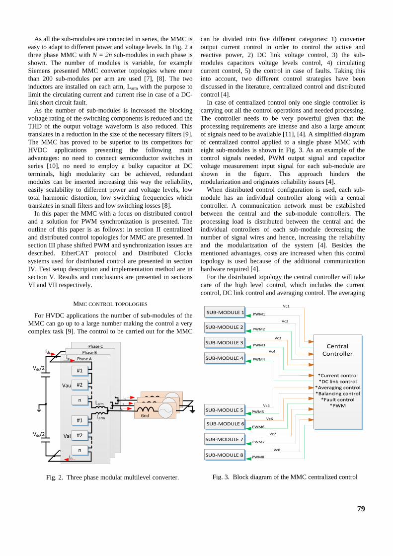
79
As all the sub-modules are connected in series, the MMC is
easy to adapt to different power and voltage levels. In Fig. 2 a
three phase MMC with N = 2n sub-modules in each phase is
shown. The number of modules is variable, for example
Siemens presented MMC converter topologies where more
than 200 sub-modules per arm are used [7], [8]. The two
inductors are installed on each arm, Larm with the purpose to
limit the circulating current and current rise in case of a DC-
link short circuit fault.
As the number of sub-modules is increased the blocking
voltage rating of the switching components is reduced and the
THD of the output voltage waveform is also reduced. This
translates in a reduction in the size of the necessary filters [9].
The MMC has proved to be superior to its competitors for
HVDC applications presenting the following main
advantages: no need to connect semiconductor switches in
series [10], no need to employ a bulky capacitor at DC
terminals, high modularity can be achieved, redundant
modules can be inserted increasing this way the reliability,
easily scalability to different power and voltage levels, low
total harmonic distortion, low switching frequencies which
translates in small filters and low switching losses [8].
In this paper the MMC with a focus on distributed control
and a solution for PWM synchronization is presented. The
outline of this paper is as follows: in section II centralized
and distributed control topologies for MMC are presented. In
section III phase shifted PWM and synchronization issues are
described. EtherCAT protocol and Distributed Clocks
systems used for distributed control are presented in section
IV. Test setup description and implementation method are in
section V. Results and conclusions are presented in sections
VI and VII respectively.
MMC CONTROL TOPOLOGIES
For HVDC applications the number of sub-modules of the
MMC can go up to a large number making the control a very
complex task [9]. The control to be carried out for the MMC
can be divided into five different categories: 1) converter
output current control in order to control the active and
reactive power, 2) DC link voltage control, 3) the sub-
modules capacitors voltage levels control, 4) circulating
current control, 5) the control in case of faults. Taking this
into account, two different control strategies have been
discussed in the literature, centralized control and distributed
control [4].
In case of centralized control only one single controller is
carrying out all the control operations and needed processing.
The controller needs to be very powerful given that the
processing requirements are intense and also a large amount
of signals need to be available [11], [4]. A simplified diagram
of centralized control applied to a single phase MMC with
eight sub-modules is shown in Fig. 3. As an example of the
control signals needed, PWM output signal and capacitor
voltage measurement input signal for each sub-module are
shown in the figure. This approach hinders the
modularization and originates reliability issues [4].
When distributed control configuration is used, each sub-
module has an individual controller along with a central
controller. A communication network must be established
between the central and the sub-module controllers. The
processing load is distributed between the central and the
individual controllers of each sub-module decreasing the
number of signal wires and hence, increasing the reliability
and the modularization of the system [4]. Besides the
mentioned advantages, costs are increased when this control
topology is used because of the additional communication
hardware required [4].
For the distributed topology the central controller will take
care of the high level control, which includes the current
control, DC link control and averaging control. The averaging
Larm
Larm
#2
n
#1
#2
n
#1
in
Vau
Val
Larm
Larm
#2
n
#1
#2
n
#1
in
Vau
Val
ia
Phase B
Phase C
Vdc/2
Vdc/2
ib
ic
Larm
Larm
#2
n
#1
#2
n
#1
in
ip
Vau
Val
Phase A
Grid
idc
Fig. 2. Three phase modular multilevel converter.
PWM1
PWM2
PWM3
PWM4
PWM5
PWM6
PWM7
PWM8
Vc1
Vc2
Vc3
Vc4
Vc5
Vc6
Vc7
Vc8
*Current control*DC link control
*Averaging control*Balancing control
*Fault control*PWM
CentralController
SUB-MODULE 1
SUB-MODULE 2
SUB-MODULE 3
SUB-MODULE 4
SUB-MODULE 5
SUB-MODULE 6
SUB-MODULE 7
SUB-MODULE 8
Fig. 3. Block diagram of the MMC centralized control
strategy.
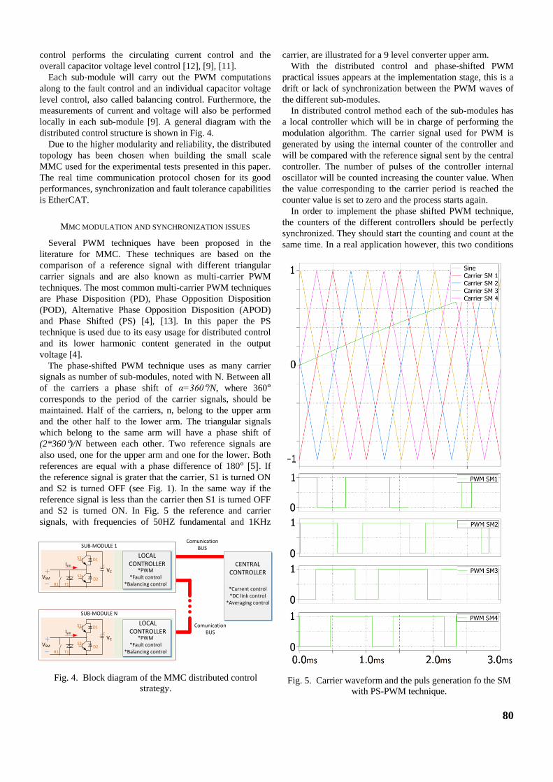
80
control performs the circulating current control and the
overall capacitor voltage level control [12], [9], [11].
Each sub-module will carry out the PWM computations
along to the fault control and an individual capacitor voltage
level control, also called balancing control. Furthermore, the
measurements of current and voltage will also be performed
locally in each sub-module [9]. A general diagram with the
distributed control structure is shown in Fig. 4.
Due to the higher modularity and reliability, the distributed
topology has been chosen when building the small scale
MMC used for the experimental tests presented in this paper.
The real time communication protocol chosen for its good
performances, synchronization and fault tolerance capabilities
is EtherCAT.
MMC MODULATION AND SYNCHRONIZATION ISSUES
Several PWM techniques have been proposed in the
literature for MMC. These techniques are based on the
comparison of a reference signal with different triangular
carrier signals and are also known as multi-carrier PWM
techniques. The most common multi-carrier PWM techniques
are Phase Disposition (PD), Phase Opposition Disposition
(POD), Alternative Phase Opposition Disposition (APOD)
and Phase Shifted (PS) [4], [13]. In this paper the PS
technique is used due to its easy usage for distributed control
and its lower harmonic content generated in the output
voltage [4].
The phase-shifted PWM technique uses as many carrier
signals as number of sub-modules, noted with N. Between all
of the carriers a phase shift of α=360ᵒ/N, where 360ᵒ corresponds to the period of the carrier signals, should be
maintained. Half of the carriers, n, belong to the upper arm
and the other half to the lower arm. The triangular signals
which belong to the same arm will have a phase shift of
(2*360ᵒ)/N between each other. Two reference signals are
also used, one for the upper arm and one for the lower. Both
references are equal with a phase difference of 180ᵒ [5]. If
the reference signal is grater that the carrier, S1 is turned ON
and S2 is turned OFF (see Fig. 1). In the same way if the
reference signal is less than the carrier then S1 is turned OFF
and S2 is turned ON. In Fig. 5 the reference and carrier
signals, with frequencies of 50HZ fundamental and 1KHz
carrier, are illustrated for a 9 level converter upper arm.
With the distributed control and phase-shifted PWM
practical issues appears at the implementation stage, this is a
drift or lack of synchronization between the PWM waves of
the different sub-modules.
In distributed control method each of the sub-modules has
a local controller which will be in charge of performing the
modulation algorithm. The carrier signal used for PWM is
generated by using the internal counter of the controller and
will be compared with the reference signal sent by the central
controller. The number of pulses of the controller internal
oscillator will be counted increasing the counter value. When
the value corresponding to the carrier period is reached the
counter value is set to zero and the process starts again.
In order to implement the phase shifted PWM technique,
the counters of the different controllers should be perfectly
synchronized. They should start the counting and count at the
same time. In a real application however, this two conditions
S1
S2VC
VSM
Ism C
D1
D2R1 T1
SUB-MODULE 1
CENTRALCONTROLLER
*Current control*DC link control
*Averaging control
LOCAL CONTROLLER
*PWM*Fault control
*Balancing control
Comunication BUS
Comunication BUS
S1
S2VC
VSM
Ism C
D1
D2R1 T1
SUB-MODULE N
LOCAL CONTROLLER
*PWM*Fault control
*Balancing control
Fig. 4. Block diagram of the MMC distributed control
strategy.
Fig. 5. Carrier waveform and the puls generation fo the SM
with PS-PWM technique.
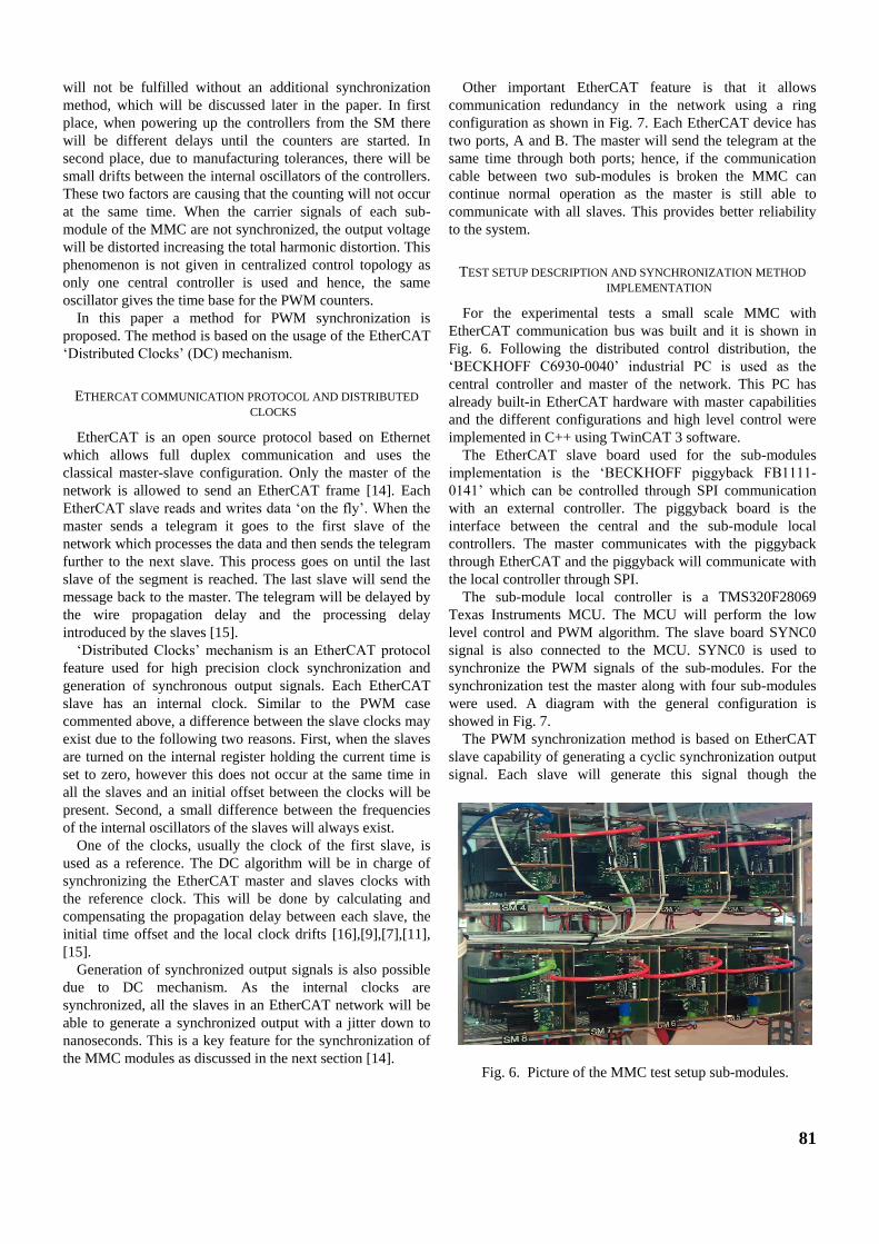
81
will not be fulfilled without an additional synchronization
method, which will be discussed later in the paper. In first
place, when powering up the controllers from the SM there
will be different delays until the counters are started. In
second place, due to manufacturing tolerances, there will be
small drifts between the internal oscillators of the controllers.
These two factors are causing that the counting will not occur
at the same time. When the carrier signals of each sub-
module of the MMC are not synchronized, the output voltage
will be distorted increasing the total harmonic distortion. This
phenomenon is not given in centralized control topology as
only one central controller is used and hence, the same
oscillator gives the time base for the PWM counters.
In this paper a method for PWM synchronization is
proposed. The method is based on the usage of the EtherCAT
‘Distributed Clocks’ (DC) mechanism.
ETHERCAT COMMUNICATION PROTOCOL AND DISTRIBUTED
CLOCKS
EtherCAT is an open source protocol based on Ethernet
which allows full duplex communication and uses the
classical master-slave configuration. Only the master of the
network is allowed to send an EtherCAT frame [14]. Each
EtherCAT slave reads and writes data ‘on the fly’. When the
master sends a telegram it goes to the first slave of the
network which processes the data and then sends the telegram
further to the next slave. This process goes on until the last
slave of the segment is reached. The last slave will send the
message back to the master. The telegram will be delayed by
the wire propagation delay and the processing delay
introduced by the slaves [15].
‘Distributed Clocks’ mechanism is an EtherCAT protocol
feature used for high precision clock synchronization and
generation of synchronous output signals. Each EtherCAT
slave has an internal clock. Similar to the PWM case
commented above, a difference between the slave clocks may
exist due to the following two reasons. First, when the slaves
are turned on the internal register holding the current time is
set to zero, however this does not occur at the same time in
all the slaves and an initial offset between the clocks will be
present. Second, a small difference between the frequencies
of the internal oscillators of the slaves will always exist.
One of the clocks, usually the clock of the first slave, is
used as a reference. The DC algorithm will be in charge of
synchronizing the EtherCAT master and slaves clocks with
the reference clock. This will be done by calculating and
compensating the propagation delay between each slave, the
initial time offset and the local clock drifts [16],[9],[7],[11],
[15].
Generation of synchronized output signals is also possible
due to DC mechanism. As the internal clocks are
synchronized, all the slaves in an EtherCAT network will be
able to generate a synchronized output with a jitter down to
nanoseconds. This is a key feature for the synchronization of
the MMC modules as discussed in the next section [14].
Other important EtherCAT feature is that it allows
communication redundancy in the network using a ring
configuration as shown in Fig. 7. Each EtherCAT device has
two ports, A and B. The master will send the telegram at the
same time through both ports; hence, if the communication
cable between two sub-modules is broken the MMC can
continue normal operation as the master is still able to
communicate with all slaves. This provides better reliability
to the system.
TEST SETUP DESCRIPTION AND SYNCHRONIZATION METHOD
IMPLEMENTATION
For the experimental tests a small scale MMC with
EtherCAT communication bus was built and it is shown in
Fig. 6. Following the distributed control distribution, the
‘BECKHOFF C6930-0040’ industrial PC is used as the
central controller and master of the network. This PC has
already built-in EtherCAT hardware with master capabilities
and the different configurations and high level control were
implemented in C++ using TwinCAT 3 software.
The EtherCAT slave board used for the sub-modules
implementation is the ‘BECKHOFF piggyback FB1111-
0141’ which can be controlled through SPI communication
with an external controller. The piggyback board is the
interface between the central and the sub-module local
controllers. The master communicates with the piggyback
through EtherCAT and the piggyback will communicate with
the local controller through SPI.
The sub-module local controller is a TMS320F28069
Texas Instruments MCU. The MCU will perform the low
level control and PWM algorithm. The slave board SYNC0
signal is also connected to the MCU. SYNC0 is used to
synchronize the PWM signals of the sub-modules. For the
synchronization test the master along with four sub-modules
were used. A diagram with the general configuration is
showed in Fig. 7.
The PWM synchronization method is based on EtherCAT
slave capability of generating a cyclic synchronization output
signal. Each slave will generate this signal though the
Fig. 6. Picture of the MMC test setup sub-modules.
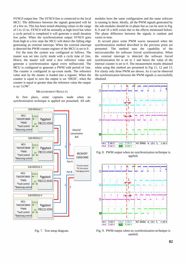
82
SYNC0 output line. The SYNC0 line is connected to the local
MCU. The difference between the signals generated will be
of a few ns. This has been tested obtaining values in the range
of 5 to 15 ns. SYNC0 will be normally at high level but when
a cycle period is completed it will generate a small duration
low pulse. When the synchronization output SYNC0 goes
from high to a low state the MCU will detect the falling edge
generating an external interrupt. When the external interrupt
is detected the PWM counter register of the MCU is set to 0.
For the tests the system was configured as follows. The
master was set into cyclic mode with a cycle time of 1ms.
Hence, the master will send a new reference value and
generate a synchronization signal every millisecond. The
MCU is configured to generate a PWM with period of 1ms.
The counter is configured in up-count mode. The reference
value sent by the master is loaded into a register. When the
counter is equal to zero the output is set ‘HIGH’, when the
counter is equal or greater than the reference value the output
is set ‘LOW’.
MEASUREMENT RESULTS
In first place, some captures made when no
synchronization technique is applied are presented. All sub-
modules have the same configuration and the same software
is running in them. Ideally, all the PWM signals generated by
the sub-modules should be in phase but as can be seen in Fig.
8, 9 and 10 a drift exists due to the effects mentioned before.
The phase difference between the signals is random and
varies in time.
In second place some PWM waves measured when the
synchronization method described in the previous point are
presented. The method uses the capability of the
microcontroller for software forced synchronization. When
the external interrupt is detected the software forced
synchronization bit is set to 1 and hence the value of the
internal counter is set to 0. The measurement results obtained
when using this method are presented in Fig 11, 12 and 13.
For clarity only three PWM are shown. As it can be observed
the synchronization between the PWM signals is successfully
obtained.
EtherCAT comunication
BUS
Port A
BECKHOFF C6930-0040
*Current control*DC link control
*Averaging control
SUB-MODULE 1
MCUTSM320F28069
*PWM*Fault control
*Balancing control
PiggybackFB1111-0141SPI
SYNC0
SUB-MODULE 2
MCUTSM320F28069
*PWM*Fault control
*Balancing control
PiggybackFB1111-0141SPI
SYNC0
SUB-MODULE 3
MCUTSM320F28069
*PWM*Fault control
*Balancing control
PiggybackFB1111-0141SPI
SYNC0
SUB-MODULE 4
MCUTSM320F28069
*PWM*Fault control
*Balancing control
PiggybackFB1111-0141SPI
SYNC0
Port B
Fig. 7. Test setup diagram.
Fig. 8. PWM output when no synchronization technique is
applied.
Fig. 9. PWM output when no synchronization technique is
applied.
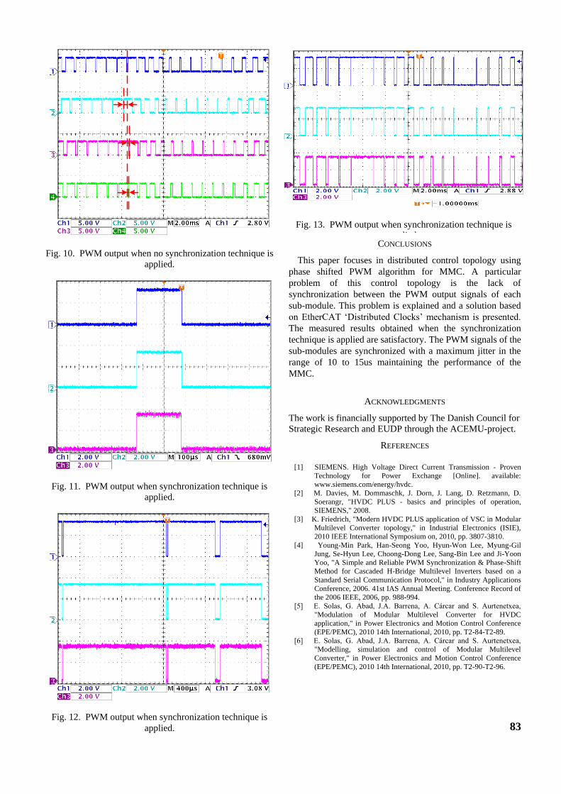
83
CONCLUSIONS
This paper focuses in distributed control topology using
phase shifted PWM algorithm for MMC. A particular
problem of this control topology is the lack of
synchronization between the PWM output signals of each
sub-module. This problem is explained and a solution based
on EtherCAT ‘Distributed Clocks’ mechanism is presented.
The measured results obtained when the synchronization
technique is applied are satisfactory. The PWM signals of the
sub-modules are synchronized with a maximum jitter in the
range of 10 to 15us maintaining the performance of the
MMC.
ACKNOWLEDGMENTS
The work is financially supported by The Danish Council for
Strategic Research and EUDP through the ACEMU-project.
REFERENCES
[1] SIEMENS. High Voltage Direct Current Transmission - Proven
Technology for Power Exchange [Online]. available:
www.siemens.com/energy/hvdc.
[2] M. Davies, M. Dommaschk, J. Dorn, J. Lang, D. Retzmann, D.
Soerangr, "HVDC PLUS - basics and principles of operation,
SIEMENS," 2008.
[3] K. Friedrich, "Modern HVDC PLUS application of VSC in Modular
Multilevel Converter topology," in Industrial Electronics (ISIE),
2010 IEEE International Symposium on, 2010, pp. 3807-3810.
[4] Young-Min Park, Han-Seong Yoo, Hyun-Won Lee, Myung-Gil
Jung, Se-Hyun Lee, Choong-Dong Lee, Sang-Bin Lee and Ji-Yoon
Yoo, "A Simple and Reliable PWM Synchronization & Phase-Shift
Method for Cascaded H-Bridge Multilevel Inverters based on a
Standard Serial Communication Protocol," in Industry Applications
Conference, 2006. 41st IAS Annual Meeting. Conference Record of
the 2006 IEEE, 2006, pp. 988-994.
E. Solas, G. Abad, .A. Barrena, A. C rcar and S. Aurtenet ea,
"Modulation of Modular Multilevel Converter for HVDC
application," in Power Electronics and Motion Control Conference
(EPE/PEMC), 2010 14th International, 2010, pp. T2-84-T2-89.
6 E. Solas, G. Abad, .A. Barrena, A. C rcar and S. Aurtenet ea,
"Modelling, simulation and control of Modular Multilevel
Converter," in Power Electronics and Motion Control Conference
(EPE/PEMC), 2010 14th International, 2010, pp. T2-90-T2-96.
Fig. 13. PWM output when synchronization technique is
applied.
Fig. 10. PWM output when no synchronization technique is
applied.
Fig. 11. PWM output when synchronization technique is
applied.
Fig. 12. PWM output when synchronization technique is
applied.
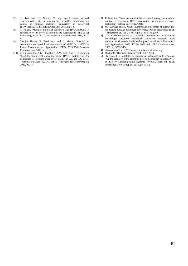
84
[7] C. Toh and L.E. Norum, "A high speed control network
synchronization jitter evaluation for embedded monitoring and
control in modular multilevel converter," in PowerTech
(POWERTECH), 2013 IEEE Grenoble, 2013, pp. 1-6.
[8] H.-.Knaak, "Modular multilevel converters and HVDC/FACTS: A
success story," in Power Electronics and Applications (EPE 2011),
Proceedings of the 2011-14th European Conference on, 2011, pp. 1-
6.
[9] Shaojun Huang, R. Teodorescu and L. Mathe, "Analysis of
communication based distributed control of MMC for HVDC," in
Power Electronics and Applications (EPE), 2013 15th European
Conference on, 2013, pp. 1-10.
[10] U. Gnanarathna, S.K. Chaudhary, A.M. Gole and R. Teodorescu,
"Modular multi-level converter based HVDC system for grid
connection of offshore wind power plant," in AC and DC Power
Transmission, 2010. ACDC. 9th IET International Conference on,
2010, pp. 1-5.
[11] E. Petre Eni, "Fault tolerant distributed control strategy for modular
multilevel converter in HVDC application - department of energy
technology, aalborg university," 2013.
[12] M. Hagiwara and H. Akagi, "Control and experiment of pulsewidth-
modulated modular multilevel converters," Power Electronics, IEEE
Transactions on, vol. 24, no. 7, pp. 1737-1746 2009.
[13] G.S. Konstantinou and V.G. Agelidis, "Performance evaluation of
half-bridge cascaded multilevel converters operated with
multicarrier sinusoidal PWM techniques," in Industrial Electronics
and Applications, 2009. ICIEA 2009. 4th IEEE Conference on,
2009, pp. 3399-3404.
[14] Anonymous EtherCAT Group : http://www.ethercat.org.
[15] Bechhoff, "Hardware data sheet ET1100," 2010.
[16] G. Cena, I.C. Bertolotti, S. Scanzio, A. Valenzano and C. Zunino,
"On the accuracy of the distributed clock mechanism in EtherCAT,"
in Factory Communication Systems (WFCS), 2010 8th IEEE
International Workshop on, 2010, pp. 43-52.