Embed Size (px)
Citation preview

Fast high-temperature superconductor switch for high current applicationsVyacheslav F. Solovyov and Qiang Li Citation: Applied Physics Letters 103, 032603 (2013); doi: 10.1063/1.4813883 View online: http://dx.doi.org/10.1063/1.4813883 View Table of Contents: http://scitation.aip.org/content/aip/journal/apl/103/3?ver=pdfcov Published by the AIP Publishing
This article is copyrighted as indicated in the article. Reuse of AIP content is subject to the terms at: http://scitation.aip.org/termsconditions. Downloaded to IP:
130.199.3.165 On: Mon, 30 Dec 2013 17:15:36
Fast high-temperature superconductor switch for high current applications
Vyacheslav F. Solovyov and Qiang LiCondensed Matter Physics and Materials Science Department, Brookhaven National Laboratory,Upton, New York 11973, USA
(Received 14 May 2013; accepted 29 June 2013; published online 16 July 2013)
Reversible operation of a high current superconductor switch based on the quench of high-resistance
second generation high temperature superconducting wire is demonstrated. The quench is induced by
a burst of an ac field generated by an inductively coupled radio-frequency coil. The switch makes a
superconducting-to-normal transition within 5 ms and also has a rapid recovery to the superconducting
state. The device has potential applications as an active current limiter or as a storage switch
for superconducting magnetic energy storage systems. Operation in a full flux penetration/flow
regime can effectively minimize the detrimental effects of the intrinsic conductor non-uniformity.VC 2013 AIP Publishing LLC. [http://dx.doi.org/10.1063/1.4813883]
An appealing feature of superconductor switching devices
is their near zero resistance, which allows a scale-up of the de-
vice to a high operating voltage and current without the penalty
of added conduction losses. A superconductor element transi-
tions from the superconducting (zero resistance) state to the
normal state (more generally, resistive state) when any one of
three factors: (i) temperature, T, (ii) current density, J, or (iii)
magnetic field, B, exceeds a certain critical value. These super-
conductor properties are widely utilized for detector,1 electric
power,2 and superconducting magnet applications.
The superconducting-to-normal transition in a fault-
current limiter (FCL) utilizes the second ambient factor, trans-
port current.3–5 The transition is triggered when the current
density at a given temperature and magnetic field exceeds the
critical current density, Jc. Since there is no external heating
involved, the transition time can be very short, less than 10 ms.
The availability of long-length (hundreds of meters) second
generation (2G) YBa2Cu3O7 (YBCO) superconducting wire6
has enabled the practical designs of in-grid FCLs operating
at 77 K.7 The transition threshold of a FCL is determined by
the lowest Jc in the whole conductor. The transport properties
of YBCO are highly sensitive to the local microstructure,
hence the Jc of 2G wire is non-uniform both along and across
the tape.8 In order to avoid damage to the conductor due to
the non-uniformity of the superconducting-to-normal transi-
tion, the superconducting element needs to be coated with a
normal metal (stabilizer), which substantially reduces the off-
resistance of the switch and raises the thermal mass of the
device.
We have developed a fast high-current switching device
that relies on the rapid superconducting transition of the
material to the normal state. This transition is induced by
a radio-frequency (RF) field created by a compact flat coil
which is inductively coupled to the superconducting layer.
This design retains the positive features of a FCL, while
minimizing the adverse effect of conductor non-uniformity,
which potentially enables the attainment of high off-resistance
values.
Fig. 1(a) is a schematic rendering of the device and Fig.
1(b) is its equivalent electrical diagram of the device. A
switching superconductor element (R1) is tightly wrapped
around a flat RF coil (L1) manufactured from 18 gauge, 175
strand Litz wire. The switching element R1 was manufactured
from a 1 m long piece of commercially available YBCO tape
(SuperPower Inc.). The middle 50 cm of the tape was stripped
of the stabilizing layers by a chemical etch, yielding the total
element resistance of 1.2 X. In the superconducting state, the
tape resistance to dc electric current generated by the power
source I1 is zero. This corresponds to the “on” state. In order
to turn the device “off” (the non-superconducting state of the
superconductor element R1), a RF generator V1 applies a
high-frequency (f¼ 100–500 kHz) voltage burst (up to 100 ms
long) to the coil L1. Large inductive currents are excited in
the superconductor due to the strong coupling of the coil to
the superconducting layer. The transition to the normal state is
triggered whenever the superposition of inductive and dc cur-
rents exceeds the critical current density of the superconduct-
ing tape. The superconducting-to-normal transition is further
assisted by hysteretic losses induced by the fast-changing
fields and Joule losses due to the rising voltage of the current
source I1. The by-pass MOSFET switches Q3 and Q4
(International Rectifier, model IRF1324S-7PPBF) were
mounted directly on the tape by the drain leads in order to pro-
vide a low-resistance current by-pass during the normal-to-
superconducting transitions. Closing of the MOSFETs Q3 and
Q4 in the “off” state of R1 allowed switch cool-down and
transition to the superconducting “on” state, thus, completing
the cycle of operation.
Fig. 2(a) presents the results of a calibration experiment
intended to determine the threshold RF power required to
drive the superconducting tape into the normal state. The RF
power level is proportional to the square of the peak-to-peak
voltage on the coil. The I-V curves of a short tape coupon are
recorded at various RF power levels. We observed a super-
conducting-to-normal transition at >7 V peak RF amplitude.
In the following experiments, we applied the RF power at
10 V, i.e., exceeding the threshold by �20%.
Fig. 2(b) shows of the RF-assisted transition speed of a
switch operating at 65 A. The RF burst at 10 V peak-to-
peak amplitude is applied for 5 ms. During the RF burst
application, the switch tape is by-passed by the closed
MOSFETs. After the application of the RF burst, the
MOSFETs are opened and the current immediately drops
from 65 A to 10 A, dropping to 3 A in 10 ms. The “off”
0003-6951/2013/103(3)/032603/3/$30.00 VC 2013 AIP Publishing LLC103, 032603-1
APPLIED PHYSICS LETTERS 103, 032603 (2013)
This article is copyrighted as indicated in the article. Reuse of AIP content is subject to the terms at: http://scitation.aip.org/termsconditions. Downloaded to IP:
130.199.3.165 On: Mon, 30 Dec 2013 17:15:36

current level is based on the 1.2 X normal state resistance
of the switch.
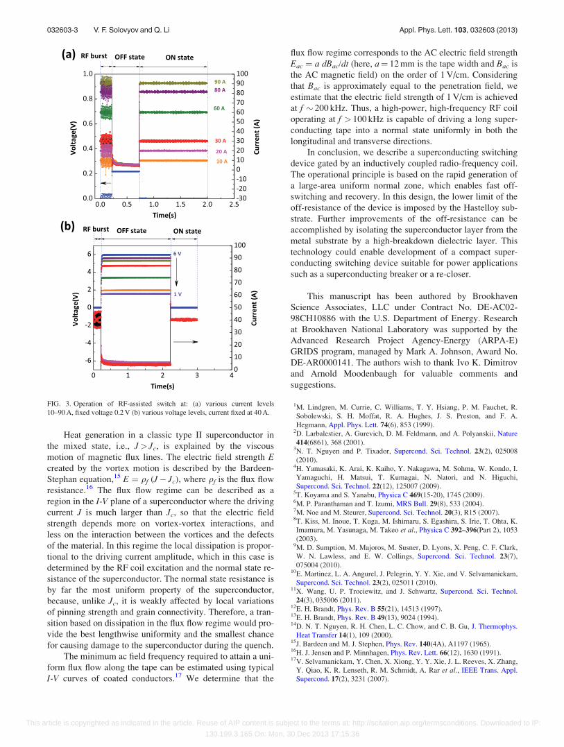
A complete cycle of operation is shown in Fig. 3(a).
Here, a 100 ms RF burst was applied to the switch operating
at various current levels, from 10 to 90 A, at a fixed voltage
of 0.2 V. The switch stayed in the “off” position for 1 s, fol-
lowed by closing of the MOSFET by-pass for 100 ms and
transition of the switch to the superconducting state. A set of
waveforms in Fig. 3(b) shows the operation of the switch
and the fixed-current level. We observe a reversible opera-
tion up to the limit of the power supply (6 V).
Device operation is based on inducing a uniform quench
of the stabilizer-free 2G wire. Without the uniform quench,
the normal zone would not have time to spread until the con-
ductor is damaged, due to the exceptionally low rate of nor-
mal zone propagation in YBCO, about 1-2 mm/s.9,10 Studies
of unprotected quenches demonstrate that the degradation of
the YBCO layer occurs at T� 490 K, primarily because of a
high level of thermal stress.11 Conductor damage can be
avoided if the superconducting layer switches to the normal
state uniformly, both along and across the tape, within a
short time, t< 200 ms.11 Our approach for creating a uniform
normal zone has two components. First, the full penetration
of the ac magnetic field into the tape assures the uniformity
of the normal zone across the tape. Second, the frequency of
the ac field is high enough to attain the flux flow regime,
which minimizes the effect of the longitudinal non-
uniformity of the tape.
The following estimation shows that the full ac field
penetration into the superconductor can be accomplished
using a lightweight flexible coil. The interaction of a thin
YBCO layer with an external ac field has been theoretically
studied by Brandt.12,13 In a strongly coupled geometry,
shown in Fig. 1(a)), an easier approach would be to treat the
interaction between the coil and the superconductor by intro-
ducing an image current. The average sheet current in the
coil would induce a mirror current in the superconductor (the
image current being superimposed on the transport current).
Even though the current density of YBCO is several magni-
tudes higher than that of copper, the equivalent sheet current
density can be attained due to the larger copper cross-sec-
tion: 1.2 lm YBCO vs. 1.02 mm for gauge 18 wire. For an
eight-turn coil excited by a current of 40 A, the sheet current
density is 320 A/cm, which is comparable with the critical
current, Ic, of the wire, at �350–380 A/cm.
Full field penetration assures the cross-wise (normal to
the tape length) transition to the normal state. However, 2G
wires are also non-uniform along the tape length on the mm
and lm scales.8 The effect of the normal zone infirmity non-
uniformity becomes critical when we consider the energy
balance between the energy dissipation in the superconduc-
tor and the heat removal by boiling nitrogen. A pool of boil-
ing nitrogen can efficiently remove up to �10 W/cm2 of heat
flux from a solid surface.14 The switch shown in Fig. 1 dissi-
pates approximately 30 W in the normal state. If we assume
a uniform dissipation, the average heat flux is �0.5 W/cm2,
which well within the safety margin for boiling nitrogen.
However, concentration of the same power in an area smaller
than 2 cm2 would lead to runaway overheating.
FIG. 1. (a) Conceptual drawing of the RF-assisted superconducting switch.
(b) An equivalent electric diagram of the device.
FIG. 2. (a) Static I-V curves of a superconducting tape at various RF power
levels (in volts on the coil). (b) Opening of the switch is induced by a 5 ms
RF burst. Note that the opening time is under 5 ms.
032603-2 V. F. Solovyov and Q. Li Appl. Phys. Lett. 103, 032603 (2013)
This article is copyrighted as indicated in the article. Reuse of AIP content is subject to the terms at: http://scitation.aip.org/termsconditions. Downloaded to IP:
130.199.3.165 On: Mon, 30 Dec 2013 17:15:36
Heat generation in a classic type II superconductor in
the mixed state, i.e., J> Jc, is explained by the viscous
motion of magnetic flux lines. The electric field strength Ecreated by the vortex motion is described by the Bardeen-
Stephan equation,15 E ¼ qf (J� Jc), where qf is the flux flow
resistance.16 The flux flow regime can be described as a
region in the I-V plane of a superconductor where the driving
current J is much larger than Jc, so that the electric field
strength depends more on vortex-vortex interactions, and
less on the interaction between the vortices and the defects
of the material. In this regime the local dissipation is propor-
tional to the driving current amplitude, which in this case is
determined by the RF coil excitation and the normal state re-
sistance of the superconductor. The normal state resistance is
by far the most uniform property of the superconductor,
because, unlike Jc, it is weakly affected by local variations
of pinning strength and grain connectivity. Therefore, a tran-
sition based on dissipation in the flux flow regime would pro-
vide the best lengthwise uniformity and the smallest chance
for causing damage to the superconductor during the quench.
The minimum ac field frequency required to attain a uni-
form flux flow along the tape can be estimated using typical
I-V curves of coated conductors.17 We determine that the
flux flow regime corresponds to the AC electric field strength
Eac ¼ a dBac/dt (here, a¼ 12 mm is the tape width and Bac is
the AC magnetic field) on the order of 1 V/cm. Considering
that Bac is approximately equal to the penetration field, we
estimate that the electric field strength of 1 V/cm is achieved
at f � 200 kHz. Thus, a high-power, high-frequency RF coil
operating at f > 100 kHz is capable of driving a long super-
conducting tape into a normal state uniformly in both the
longitudinal and transverse directions.
In conclusion, we describe a superconducting switching
device gated by an inductively coupled radio-frequency coil.
The operational principle is based on the rapid generation of
a large-area uniform normal zone, which enables fast off-
switching and recovery. In this design, the lower limit of the
off-resistance of the device is imposed by the Hastelloy sub-
strate. Further improvements of the off-resistance can be
accomplished by isolating the superconductor layer from the
metal substrate by a high-breakdown dielectric layer. This
technology could enable development of a compact super-
conducting switching device suitable for power applications
such as a superconducting breaker or a re-closer.
This manuscript has been authored by Brookhaven
Science Associates, LLC under Contract No. DE-AC02-
98CH10886 with the U.S. Department of Energy. Research
at Brookhaven National Laboratory was supported by the
Advanced Research Project Agency-Energy (ARPA-E)
GRIDS program, managed by Mark A. Johnson, Award No.
DE-AR0000141. The authors wish to thank Ivo K. Dimitrov
and Arnold Moodenbaugh for valuable comments and
suggestions.
1M. Lindgren, M. Currie, C. Williams, T. Y. Hsiang, P. M. Fauchet, R.
Sobolewski, S. H. Moffat, R. A. Hughes, J. S. Preston, and F. A.
Hegmann, Appl. Phys. Lett. 74(6), 853 (1999).2D. Larbalestier, A. Gurevich, D. M. Feldmann, and A. Polyanskii, Nature
414(6861), 368 (2001).3N. T. Nguyen and P. Tixador, Supercond. Sci. Technol. 23(2), 025008
(2010).4H. Yamasaki, K. Arai, K. Kaiho, Y. Nakagawa, M. Sohma, W. Kondo, I.
Yamaguchi, H. Matsui, T. Kumagai, N. Natori, and N. Higuchi,
Supercond. Sci. Technol. 22(12), 125007 (2009).5T. Koyama and S. Yanabu, Physica C 469(15-20), 1745 (2009).6M. P. Paranthaman and T. Izumi, MRS Bull. 29(8), 533 (2004).7M. Noe and M. Steurer, Supercond. Sci. Technol. 20(3), R15 (2007).8T. Kiss, M. Inoue, T. Kuga, M. Ishimaru, S. Egashira, S. Irie, T. Ohta, K.
Imamura, M. Yasunaga, M. Takeo et al., Physica C 392–396(Part 2), 1053
(2003).9M. D. Sumption, M. Majoros, M. Susner, D. Lyons, X. Peng, C. F. Clark,
W. N. Lawless, and E. W. Collings, Supercond. Sci. Technol. 23(7),
075004 (2010).10E. Martinez, L. A. Angurel, J. Pelegrin, Y. Y. Xie, and V. Selvamanickam,
Supercond. Sci. Technol. 23(2), 025011 (2010).11X. Wang, U. P. Trociewitz, and J. Schwartz, Supercond. Sci. Technol.
24(3), 035006 (2011).12E. H. Brandt, Phys. Rev. B 55(21), 14513 (1997).13E. H. Brandt, Phys. Rev. B 49(13), 9024 (1994).14D. N. T. Nguyen, R. H. Chen, L. C. Chow, and C. B. Gu, J. Thermophys.
Heat Transfer 14(1), 109 (2000).15J. Bardeen and M. J. Stephen, Phys. Rev. 140(4A), A1197 (1965).16H. J. Jensen and P. Minnhagen, Phys. Rev. Lett. 66(12), 1630 (1991).17V. Selvamanickam, Y. Chen, X. Xiong, Y. Y. Xie, J. L. Reeves, X. Zhang,
Y. Qiao, K. R. Lenseth, R. M. Schmidt, A. Rar et al., IEEE Trans. Appl.
Supercond. 17(2), 3231 (2007).
FIG. 3. Operation of RF-assisted switch at: (a) various current levels
10–90 A, fixed voltage 0.2 V (b) various voltage levels, current fixed at 40 A.
032603-3 V. F. Solovyov and Q. Li Appl. Phys. Lett. 103, 032603 (2013)
This article is copyrighted as indicated in the article. Reuse of AIP content is subject to the terms at: http://scitation.aip.org/termsconditions. Downloaded to IP:
130.199.3.165 On: Mon, 30 Dec 2013 17:15:36