Embed Size (px)
Citation preview

A FAST FPGA DEVELOPMENT OF RSD BASED ECC PROCESSOR*P HARI GURU PRASAD ** KRISHNA MOHAN
PG Scholar, Dept of ECE, VLSI-D, Sri Venkateswara College of Engineering, Tirupathi, Andhra Pradesh, India.Email: [email protected]
ABSTRACT— In this paper, an exportable application-particular education-set elliptic curve cryptography processor primarily based on redundant signed digit illustration is proposed. The processor employs extensive pipelining strategies for Karatsuba–Of man approach to obtain excessive throughput multiplication. Furthermore, an green modular adder with out contrast and a excessive throughput modular divider, which results in a brief facts path for maximized frequency, are carried out. The processor supports the advocated NIST curve P256 and is based on an prolonged NIST discount scheme. The proposed processor performs single point multiplication using points in affine coordinates in 2.26 ms and runs at a maximum frequency of one hundred sixty MHz in Xilinx Virtex 5 (XC5VLX110T) area-programmable gate array.
Index Terms—Application-specific instruction-set processor (ASIP), elliptic curve cryptography (ECC), field-programmable gate array (FPGA), Karatsuba–Ofman multiplication, redundant signed digit (RSD).
I. INTRODUCTION Elliptical curve cryptography (ECC) is an
asymmetric cryptographic device that offers an equal security to the famous Rivest, Shamir and Adleman machine with a lot smaller key sizes. The fundamental operation in ECC is scalar factor multiplication, in which a point on the curve is improved by means of a scalar. A scalar factor multiplication is performed with the aid of calculating series of factor additions and point doublings. Using their geometrical properties, factors are added or doubled via series of additives, subtractions, multiplications, anddivisions in their respective coordinates. Point coordinates are the factors of finite fields closed beneath a top or an irreducible polynomial. Various ECC processors had been proposed within the literature that both goal binary fields top fields or dual subject operations.Carry good judgment or embedded virtual sign processing (DSP) blocks inside discipline programmable gate arrays (FPGAs) are also applied in a few designs to deal with the bring propagation hassle. It is important to construct an green addition facts course in view that it is a essential operation employed in different modular arithmetic operations.In order to optimize the multiplication
method, a few ECC processors use thedivide and conquer approach of Karatsuba of man multiplications, where others use embedded multipliers and DSP blocks inside FPGA fabric. In high subject ECC processors, bring unfastened arithmetic is necessary to avoid prolonged information paths as a result of bring Propagation. Modular multiplication is an crucial operation in ECC processor. There are two kinds one is as interleaved modular multiplication the use of Bernard Law Montgomery’smethod when arbitrary curves are required and some other is multiply-then-reduce and is used in elliptic curves constructed over finite fields of Mersseneprimes which lets in green modular reduction reduction thru series of additions and subtraction. Since modular department in affine coordinates is a costlyprocess, different techniques are proposed to compensate the price like jacobian co-ordinate and fermat’s little theorem. ECC processor also use GSD set of rules. Hence, many ECC processors with combined modular division and multiplication blocks were proposed.The complexity of modular division algorithms is approximately O(2n), wherein n is the size of operands and the strolling time is variable and relies upon immediately on the inputs.II. PROPOSED SYSTEM:
Due to the dangers of long variety information paths and brief frequency variety in present current systems, a way is proposed to boom frequency variety and decrease the data path variety.This paper proposes a new RSD-based high subjectECC processor with high-pace running frequency.
The processor is an utility-particular education-set processor (ASIP) type to provide programmability and configurability. In this paper, we reveal the overall performance of left-to-right scalar factor multiplication algorithm; however, the ASIP characteristic of the processor allows extraordinary algorithms to be performed via the thru examine-best reminiscence (ROM) programming. The universal processor architecture is of ordinary go bar type with 256 digit huge information buses. The layout method and optimization strategies are focused in the direction of efficient individual modular arithmetic modules in preference to the general architecture. Such architecture permits for clean alternative of man or woman blocks if distinct algorithms or modular arithmetic techniques are

preferred. Different efficient architectures of person modular mathematics blocks for diverse algorithms are proposed. The novelty of our processor evolves round the subsequent.
1) We introduce the first FPGA implementation of RSD-based ECC processor.2) Extensive pipelining and optimization strategies are used to acquire a high-throughput iterative Karatsuba multiplier which lead to a performance improvement of just about a hundred% over the processor proposed in.Three) To the best of our expertise, the proposed modular department/inversion is the quickest to be accomplished on FPGA tool. This is executed through a new green binary GCD divider architecture based on easy logical operations.4) A modular addition and subtraction is proposed without contrast.5) Most importantly, exportable layout is proposed with specially designed multipliers and convey unfastened adders that provided in aggressive results against DSPs and embedded multipliers-based designs.III. Related work:Elliptic curve cryptography: It is a public key cryptography based totally on algebraic shape of elliptic curves over finite fields and requires smaller keys to provide equal security. For present day cryptographic functions, an elliptic curve is a plane curve over a finite field which includes points enjoyable the equation along side a distinguished factor at infinity.
Ε ∶ y2=x3+ax+b
The smoothness of the curve and distinct roots are guaranteed by 4 a3+27 b2≠ 0.Point coordinates are of type integers for an elliptic curve defined by above equation and are the elements of an underlying finite field with operations performed modulo a prime number. Such elliptic curves are known as prime field elliptic curves.
Point Scalar Multiplication:
Point scalar multiplication is the operation of multiplying a point P on the elliptic curve by an integer scalar k within the underlying field. The operation is performed as k-times addition of the point P to itself. A discrete logarithm problem is formulated based on the scalar point multiplication and several cryptographic protocols and algorithms have been established accordingly.
Algorithm 1Algorithm 1 is based on the square-and-multiply method for the exponentiation, where the exponent is scanned from left to- right and the operations of squaring and/or multiplication are performed according to the binary value of the scanned bit. The operations of squaring and multiplication are replaced by point doubling and point addition, respectively.
Redundant Signed Digits The RSD representation is a carry free arithmetic where integers are represented by the difference of two other integers. An integer X is represented by the difference of its x+ and x−components, where x+ is the positive component and x−is the negative component. The nature of the RSD representation has the advantage of performing addition and subtraction without the need of the two’s complement representation. On the other hand, an overhead is introduced due to the redundancy in the integer representation, since an integer in RSD representation requires double wordlength compared with typical two’s complement representation. In radix-2 balanced RSD represented integers, digits of such integers are either 1,0 or -1.Karatsuba–Ofman Multiplication:
The complexity of the regular multiplication using the schoolbook method is O(n2). Karatsuba and Ofman proposed a methodology to perform a multiplication with complexity O(n1.58) by dividing the operands of the multiplication into smaller and equal segments. Having two operands of length n to be multiplied, the Karatsuba–Ofman methodologysuggests to split the two operands into high-(H) and low-(L).The original Karatsuba algorithm is performed recursively, where the operands are segmented into smaller parts until a reasonable size is reached, and then regular multiplications of the smaller segments are performed recursively.
Binary GCD Modular Division:This algorithm is considered as the basis for
several hardware implementations of modular division. Algorithm 2 computes the modular division Z ≡X/Y (mod M) based on the plus– minus version of the original binary GCD algorithm. The algorithm instantiates the four registers A, B,U, and V that

are initialized with Y, M, X, and 0, respectively. Then, it constantly reduces the values of Y and M in order to calculate the GCD(Y, M) which is equal to 1 in well formed elliptic curves where the modulo is prime. The registers U and V are used to calculate the quotient and the operations performed on these registers are similar to the operations performed on the A and B registers. The operations on the registers A and B are performed by repetitively reducing the contents of both registers by simple shift or add/subtract-shift operations based on the conditions whether the intermediate contents are even or not. In the case where both registers contents are odd, the content of both registers are added if A+B is divisible by 4 or subtracted, (A−B), otherwise. Two variables ρ and δ are used to control the iterations of the algorithm based on the bounds of the registers contents, where δ = α −β, 2α and 2β are the upper bounds of A and B, respectively, and ρ = min(α, β).
Algorithm 2
OVERALL PROCESSOR ARCHITECTURE
The proposed P256 ECC processor consists of an AU of 256 RSD digits wide, an finite-state machine
(FSM), memory, and two data buses. The processor can be configured in the pre synthesis phase to support the P192 or P224 NIST recommended prime curves processor architecture. Two sub control units are attached to the main control unit as add-on blocks. These two sub control units work as FSMs for point addition and point doubling, respectively.Different coordinate systems are easily supported byadding corresponding sub control blocks that operate according to the formulas of the coordinate system.External data enter the processor through the external bus to the 256 RSD digits input bus. Data are sent in binary format and a binary to RSD converter stuffs zeros in between the binary bits in order to create the RSD representation. Hence, 256-bits binary represented integers are converted to 512-bits RSD represented integers. To convert RSD digits to binary format, one needs to subtract the negative component from the positive component of the RSD digit.
Fig.1. Overall processor architecture
IV. ARITHMETIC UNITThe AU is the core unit of the processor that
includes the following blocks: 1) modular addition/subtraction block2) modular multiplication block and 3)modular division block.A. Modular Addition and SubtractionAddition is used in the accumulation process during themultiplication, as well as, in the binary GCD modular divider algorithm. In the proposed implementation, radix-2 RSD representation system as carry free representation is used. In RSD withradix-2, digits are represented by 0, 1, and −1, where digit 0is coded with 00, digit 1 is coded with 10, and digit −1 iscoded with 01.An RSD adder is presented that is built from generalized full adders. The problem with this adder is that it tends to expand the addition result even if there is no overflow, since it restricts the least significant digit (LSD) to be digit −1 only. This unnecessary overflow affects the reduction process later and produces some control complexities in the overall processor architecture.

However,the overflow is easily managed when the adder is instantiated as a subblock within a multiplier or a divider as is the case in the proposed implementation.In order to overcome the problem of overflow introduced a method is proposed consists of two layers, where layer 1 generates the carry and the interim sum, and layer 2 generates the sum, as shown
Fig.2.RSD adder/subtractorThe advantage of the proposed modular addition scheme is that only the MSD digits of the intermediate results are checked for the reduction process. Our modular adder/subtracter consists of one full word RSD adder, two full word multiplexers, and one register with some control signals. One modular addition/subtraction is performed within one, two, or three clock cycles as per the value of the MSD that is retrieved after every addition.
Fig.3. Modular addition subtraction block diagram
Modular MultiplicationKaratsuba’s multiplier recursive nature is considereda major drawback when implemented in hardware.Hardware complexity increases exponentially with thesize of the operands to be multiplied. To overcome this drawback, Karatsuba method is applied at two levels. A recursive Karatsuba block that works depthwise, and an iterative Karatsuba that works
widthwise. The proposed method consists of two phases: 1) in phase 1, a regular recursive Karatsuba is built through recursive construction down to 1-digit level and 2) the recursive Karatsuba block is used to perform Karatsuba multiplications iteratively. Hence,three recursive Karatsuba blocks are used to perform single widthwise Karatsuba iteration.
Fig.4. Karatsuba recursive block diagram
Fig.5. The recursive construction of theKaratsuba multiplication method
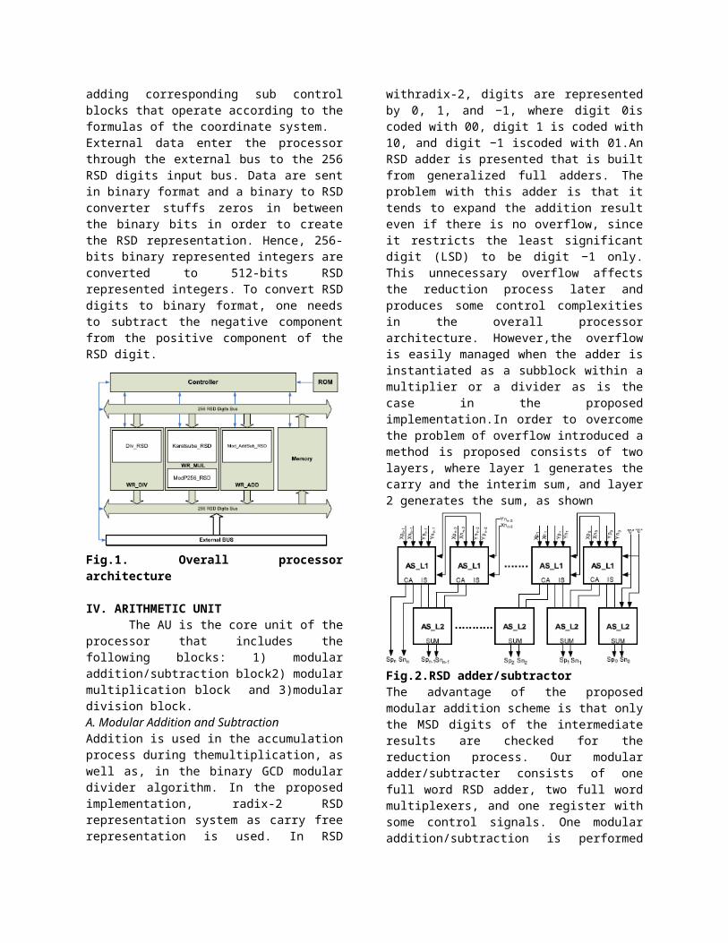
Fig.6. Iterative-recursive karatsuba multiplier
High-Radix Modular Division:Binary GCD algorithm is an efficient way of
performing modular division since it is based on addition, subtraction, and shifting operations. The complexity of the division operation comes from the fact that the running time of the algorithm isinconsistent and is input dependent. As seen in Algorithm 2, three main states define the flow of the algorithm. In the first state, the divider is checked whether it is even or odd. In the second state, the content of the corresponding registers are swapped according to the flag δ. In the last state, division by 4 modulo M is performed. In order to efficiently implement Algorithm 2 in hardware, the following list of operations should be adopted to be executed efficiently in hardware. First, division by 2 or by 4 is simply performed by shifting to right 1-digit/2-digitsaccordingly based on the guarantee that the LSDs are zerosin line 3 and 12 of the algorithm. On the other hand, division by 2 modulo M (division by 4 modulo M) is performed by adding or subtracting the dividend to or from the modulus according to whether the dividend is even or odd and the value of M (mod 4). For both δ and ρ, a comparison with 0 is necessary. However, an efficient alternative is to initialize a vector of size n with all zeros except the least significantbyte (LSB) for δ and the most significant byte (MSB) for ρ. Hence, the counting down of ρ is performed by shifting 1 bit to right and only the LSB is checked for the loop termination. On the other hand, a flag is needed to control the shift direction of δ, where the flag and the value of the LSB are used to determine whether it is less than zero or not. Theimplementation of the algorithm follows the implementation proposed in. The modular divider architecture is shown.
Fig.7.Modular divider block
V. CONTROL UNIT AND INSTRUCTION SETThe control unit consists of the main
controller of the processor that is an FSM. It also includes two processing units that control the procedures for the point doubling and point addition. In order to process the different coordinate systems, the other processing units can be generated to support them as an add-on feature. Hence, new instructions need to be added to the instruction set to accommodate the new processing units. Different scalar point multiplication algorithms are supported at instruction level. Different projective coordinate systems and point addition/doubling variations are configured at the control level through add-on processing units. On the other hand, elliptic curves with different finite fields are supported as a presynthesis process.
Main Controller:The primary task of the main controller is to
fetch, read, and execute instructions from memory. Based on the flow of instructions, the two attached processing units for point doubling and point addition are controlled accordingly. During the running time of the point doubling and point addition, control signals for the AU blocks and the memory are generated.
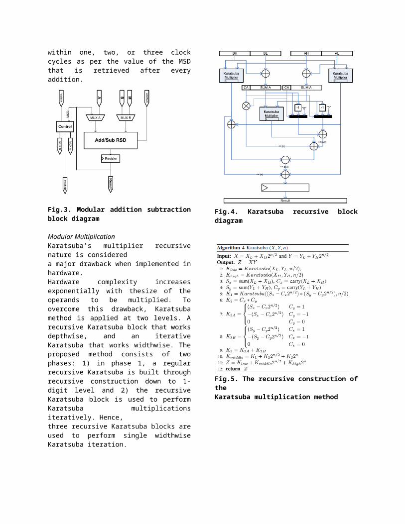
Fig.8. Main controller fsm block
Point Addition/Doubling Controller:The point addition/doubling processing units
are subroutines that control the sequence of operations for affine coordinate system. These subroutines are the part of the main controller and are made as add-on blocks for customization purposes. They mainly control the execution order of the AU blocks in order to obtain the resultant coordinates of adding two points or doubling a point. The coordinates of these two points reside in the first half of the memory, where the second half is used for storing the intermediate results from the AU. The flow and sequence of operations controlled by the point addition or point doubling controllers and the intermediate contents of the memory registers are shown
Fig.9. Point addition and doubling process flow
ROM and Instruction Set:The instruction set defined for our processor
is at point multiplication level, where the main instructions represent point doubling and point addition operations. The other choice was to implement the instruction set at the arithmetic level; however, complexity increases as a cost for increased flexibility. Instructions are 16-bits wide, the MSB is used for the operation, and the LSB is used for operands. Initially, point doubling and point addition instructions are defined with the possibility to expand the instruction set to include other coordinate systems operations. In addition, the instruction set can be extended to include simple power analysis (SPA)counter measures. For instance, other point addition and point doubling (XPA and XPD) are added to the instruction set that perform dummy operations to provide the balance needed to counteract an SPA attacks. The regular point addition requires 6 additions, 2 multiplications, and 1 division, where point doubling requires 8 additions, 3 multiplications, and1 division. Hence, 1 dummy multiplications and 2 additions are added to XPA instruction to balance the point doublingwith the point addition operation. Table III presents the instruction set with their operations and hexadecimal codes along with the clock cycles and their timings. A ROM is used to hold the assembly code that represents a certain point multiplication algorithm. The code is loaded into ROM as a pre synthesis process.
VI. RESULTS:
Fig: Processor design
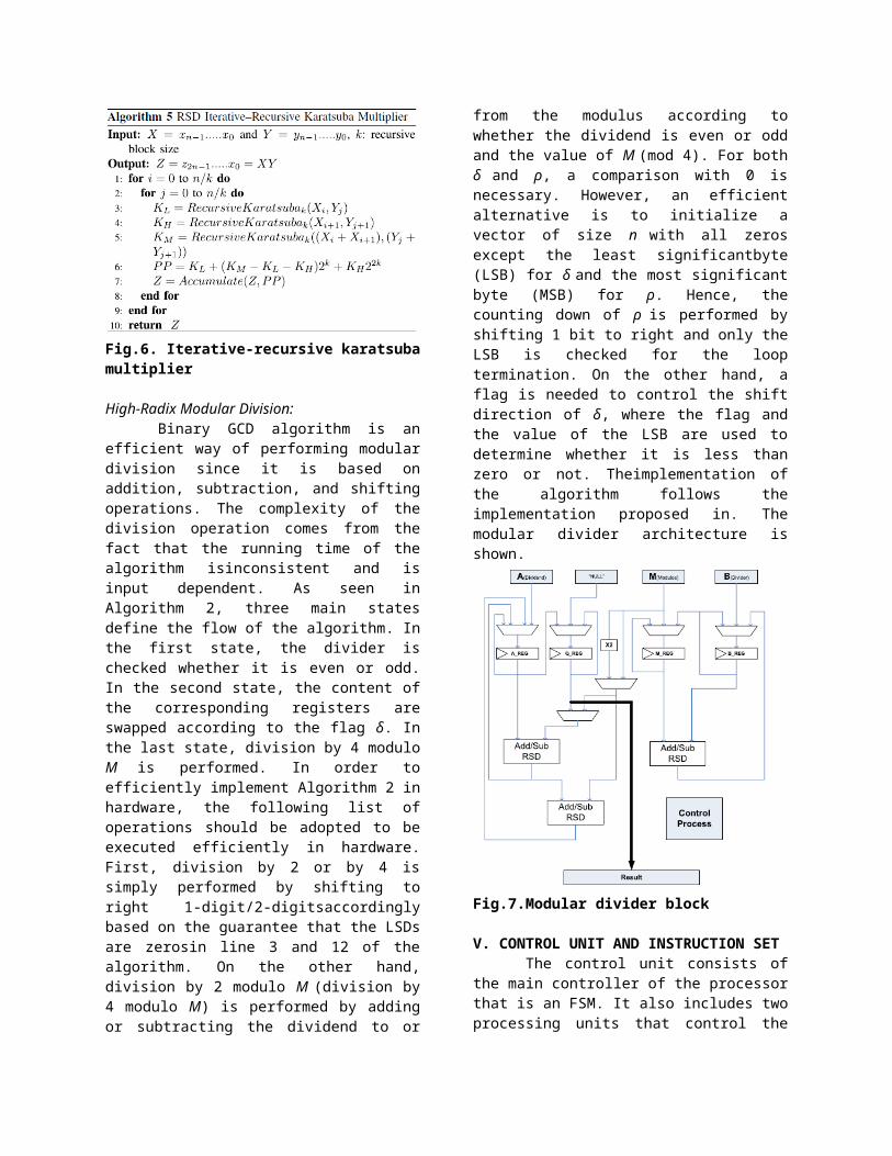
Fig:processor design by using logic gates
Fig: waveforms of ALU operations
VII.CONCLUSION:In this paper, a NIST 256 prime field ECC
processor implementation in FPGA has been presented. An RSD as a carry free representation is utilized which resulted in short data paths and increased maximum frequency. We introduced enhanced pipelining techniques within Karatsuba multiplier to achieve high throughput performance by a fully LUT-based FPGA implementation. An efficient binary GCD modular divider with three adders and shifting operations is introduced as well. Furthermore, an efficient modular addition/subtraction is introduced based on checking the LSD of the operands only. A control unit with add-on like architecture is proposed as a reconfigurability feature to support different point multiplication algorithms and coordinate systems. The implementation results of the proposed processor showed the shortest datapath with a maximum frequency of 160 MHz, which is the fastest reported in the literature for ECC processors with fully LUT-

based design. A single point multiplication is achieved by the processor within 2.26 ms, which is comparable with ECC processors that are based on embedded multipliers and DSP blocks within the FPGA. The main advantages of our processor include the exportability to other FPGA and ASIC technologies and expandability to support different coordinate systems and point multiplicationalgorithms.
REFERENCES:
[1] N. Koblitz, “Elliptic curve cryptosystems,” Math. Comput., vol. 48,no. 177, pp. 203–209, Jan. 1987.
[2] W. Stallings, Cryptography and Network Security: Principles and Practice, 5th ed. Englewood Cliffs, NJ, USA: Prentice-Hall, Jan. 2010.
[3] C. Rebeiro, S. S. Roy, and D. Mukhopadhyay, “Pushing the limitsof high-speed GF(2m) elliptic curve scalar multiplication on FPGAs,”in Proc. Cryptograph. Hardw.Embedded Syst. (CHES), vol. 7428.Jan. 2012, pp. 494–511.
[4] Y. Wang and R. Li, “A unified architecture for supporting operationsof AES and ECC,” in Proc. 4th Int. Symp. Parallel Archit., AlgorithmsProgramm. (PAAP), Dec. 2011, pp. 185–189.
[5] S. Mane, L. Judge, and P. Schaumont, “An integrated prime-field ECDLP hardware accelerator with high-performance modular arithmetic units,”in Proc. Int. Conf. Reconfigurable Comput. FPGAs, Nov./Dec. 2011,pp. 198–203.
[6] M. Esmaeildoust, D. Schinianakis, H. Javashi, T. Stouraitis, and K. Navi,Efficient RNS implementation of elliptic curve point multiplication overGF(p),” IEEE Trans. Very Large Scale Integr. (VLSI) Syst., vol. 21, no. 8,pp. 1545–1549, Aug. 2012.
[7] D. M. Schinianakis, A. P. Fournaris, H. E. Michail, A. P. Kakarountas,and T. Stouraitis, “An RNS implementation of an Fpelliptic curve point multiplier,” IEEE Trans. Circuits Syst. I, Reg. Papers, vol. 56, no. 6,pp. 1202–1213, Jun. 2009.
[8] J.-W. Lee, S.-C.Chung, H.-C.Chang, and C.-Y. Lee, “Efficient poweranalysis-resistant dual-field elliptic curve cryptographic processor usingheterogeneous dual-processing-element architecture,” IEEE Trans. VeryLarge Scale Integr. (VLSI) Syst., vol. 22, no. 1, pp. 49–61, Feb. 2013.