Embed Size (px)
Citation preview
Fast and Efficient Purification for Highly Conductive Transparent Carbon Nanotube Films
Ju Yeon Woo,† Duckjong Kim,† Joondong Kim,† Jongkyoo Park,‡ and Chang-Soo Han*,†
Department of Nano-Mechanics, Korea Institute of Machinery and Materials (KIMM), Daejeon 305-343, Korea, andComposite Laboratory, Agency for Defense DeVelopment (ADD), Daejeon 305-600, Korea
ReceiVed: May 10, 2010; ReVised Manuscript ReceiVed: October 1, 2010
A combination of thermal oxidation and thermal recovery was used to obtain transparent single-walled carbonnanotube (SWCNT) films with low sheet resistance. The process resulted in the effective removal of impuritiesand healing of defects in the SWCNTs, thus markedly increasing their conductivity. SWCNT samples beforeand after the process were analyzed by Raman spectroscopy, scanning and transmission electron microscopy,thermogravimetric analysis, contact angle measurement, and transparent conductive film fabrication. Followingpurification, the sheet resistance decreased from 5380 to 187 Ω/sq at 80% optical transmittance and at awavelength of 550 nm. The process requires a short time of about 3 h and produces 30% yield of the as-produced sample.
Introduction
Because of their unique physical, chemical, electrical, andmechanical properties, single-walled carbon nanotubes haveattracted the attention of researchers for various potentialapplications such as display, energy devices, tools in nanotech-nology, sensors, electronic devices, and composites.1–5 Thin,optically transparent, and highly conductive carbon nanotubefilms have been studied widely for replacing indium tin oxide.6
Among several types of CNT, transparent conducting film (TCF)made of arc-discharge SWNTs presents the best performanceof any CNT, such as CVD grown SWCNT, double-walled CNT,and multiwalled CNT.7 Yet the arc-discharge SWCNT isexpensive so that one should be careful not to lose too muchSWCNT during the purification process before TCF fabrication.However, to obtain the optimal performance of SWCNTs invarious applications or studies, the high yielding purificationof SWCNTs is critical.
The impurities found typically in as-produced SWCNTs bythe arc discharge method include byproduct (fullerenes, amor-phous carbon, and carbon shells) and residues of precursormaterials (graphite flakes or metal catalysts).8 These structuraldefects and impurities on SWCNTs deteriorate their typicalproperties and have restricted practical application of SWCNTfilms.9 Although there are many reports about the purificationof SWNT and its application to TCF, investigation of the effectof each purification step before TCF fabrication, such as thermaloxidation, acid treatment, and recovery, has not been reported.Important factors for purification include process time, weightloss, and performance of the film. One could sacrifice theprocess time and weight loss to obtain high performance of TCFthrough a severe purification process, but if the TCF alreadymeets the performance requirements, for example, of a touchpanel, then the next requirement would be to minimize processtime and weight loss. Accordingly, in this study, we suggest anovel purification process considering all three factors. As shownin Figure 1, the typical purification process before film fabrica-
tion follows thermal oxidation, acid treatment, and thencentrifugation.
In this Article, we did not consider the doping process andacid treatment. A doping process could be added to enhancethe conductivity of the TCF.10,11 However, the doped materialsappear to be unstable for long-term exposure to air, so thisprocess is problematic for industrial application.12 The usualpurification method generally includes an acid treatment processto remove the metal catalysts, which might induce surfacedamage on the CNT wall. With respect to TCF fabrication, howthe severe acid purification before film fabrication relates tothe conductivity of TCF remains unclear. In our experiments,acid treatment before thermal recovery showed no effect on thesheet resistance of TCF.
Herein, we suggest an effective purification and recovery ofSWCNTs produced by the arc-discharge method, performedusing a combination of thermal oxidation and high temperatureannealing without acid treatment. Using only thermal oxidationand centrifugation, we could achieve 540 Ω/sq of sheetresistance at 80% transmittance. In addition, we introduced a
* Corresponding author. Phone: +82-42-868-7126. Fax: +82-42-868-7123. E-mail: [email protected].
† KIMM.‡ ADD.
Figure 1. Flowchart of the process for obtaining highly conductivetransparent SWCNT film. Instead of acid treatment, we applied athermal recovery process to improve the conductivity of SWCNTs. Thetotal process time takes 3 h before making the film.
J. Phys. Chem. C 2010, 114, 19169–19174 19169
10.1021/jp107691q 2010 American Chemical SocietyPublished on Web 10/22/2010
thermal recovery process to heal the defects on SWCNTs, whichresulted in a marked reduction in the sheet resistance of thefabricated film by about 3-fold. The overall process time beforefilm fabrication takes 3 h, which is not too long to be appliedto a realistic manufacturing process. After the thermal processes,the remaining quantity of SWCNTs was about 30% of the as-produced (hereafter, AP) sample (Figure 1). We believe thatthe proposed processes are effective in view of the realproduction of TCF.
Experimental Details
Materials and Preparation of TCF Films. As-producedSWCNTs made by arc-discharge were provided by TopnanosysInc. (Korea). We conducted preliminary experiments at varioustemperatures (350, 400, 800, 900, 1000, 1300, and 1400 °C),times (30 min, 1 h, 3 h), and with various gases (vacuum,ammonia flow, Ar flow) to find optimal conditions of oxidationand heat treatment. The best results were obtained at 400 °Cfor 30 min under an oxygen flow in case of oxidation and at1000 °C under Ar flow for 1 h in case of heat treatment. First,
for the purification of SWCNTs, thermal oxidization (hereafter,TO) was conducted at 400 °C for 30 min under an oxygen flowto remove carbonaceous particles. For both AP-SWCNTs andTO-SWCNTs, thermal recovery (hereafter, TR) was then carriedout at 1000 °C under Ar flow for 1 h to heal the defects on theSWCNTs, as well as to remove additional impurities. For allheat-treated samples, a mixture of 0.08 mg/mL SWCNTs and10 mg/mL sodium dodecyl sulfate (SDS) dispersed in doublydeionized (DI) water was tip-sonicated for 30 min. Thesurfactant, SDS, was purchased from Sigma-Aldrich and usedas received. The SWCNT solution was then centrifuged at10 000 rpm for 1 h to remove large impurities, and thesupernatant was decanted carefully. Finally, the suspension wascollected by membrane filtration (pore size, 0.1 um), which hasbeen applied widely to TCF fabrication.13,14 The fabricated filmwas washed with DI water several times. To remove the filter,a NaOH solution was used, and the floating film was thentransferred onto a glass slide. Table 1 summarizes the processtime, the final yield, and carbon content for each step.
Measurement Methods. Raman spectra were measured usingan inVia Raman system (Renishaw Co.) equipped with 633 nmexcitation laser sources. Carbon nanotube morphology wascharacterized using FE-SEM (Sirion model, FEI Co.) and FE-TEM (Tecnai G2 F30 S-Twin model, FEI Co.). Energydispersive spectroscopy (EX-200, Horiba) analysis was used toanalyze carbon content and other impurities. The thermalbehavior of SWCNTs was monitored by thermogravimetry (TG209 F3, Netzsch Inc.). Sheet resistance of the thin conductivefilm was measured using the four-point probe method (CMT-100MP, AIT Co.), and the optical transmittance was character-
TABLE 1: Process Time, Final Yield, and Carbon Contentfor Each Step
process time (h)(including dispersion and
centrifugation time) yield (%)carbon
content (at. %)
AP 1.5 100 72.83TR 1 61 47.12TO 0.5 48 54.69TO-TR 3 30 59.35
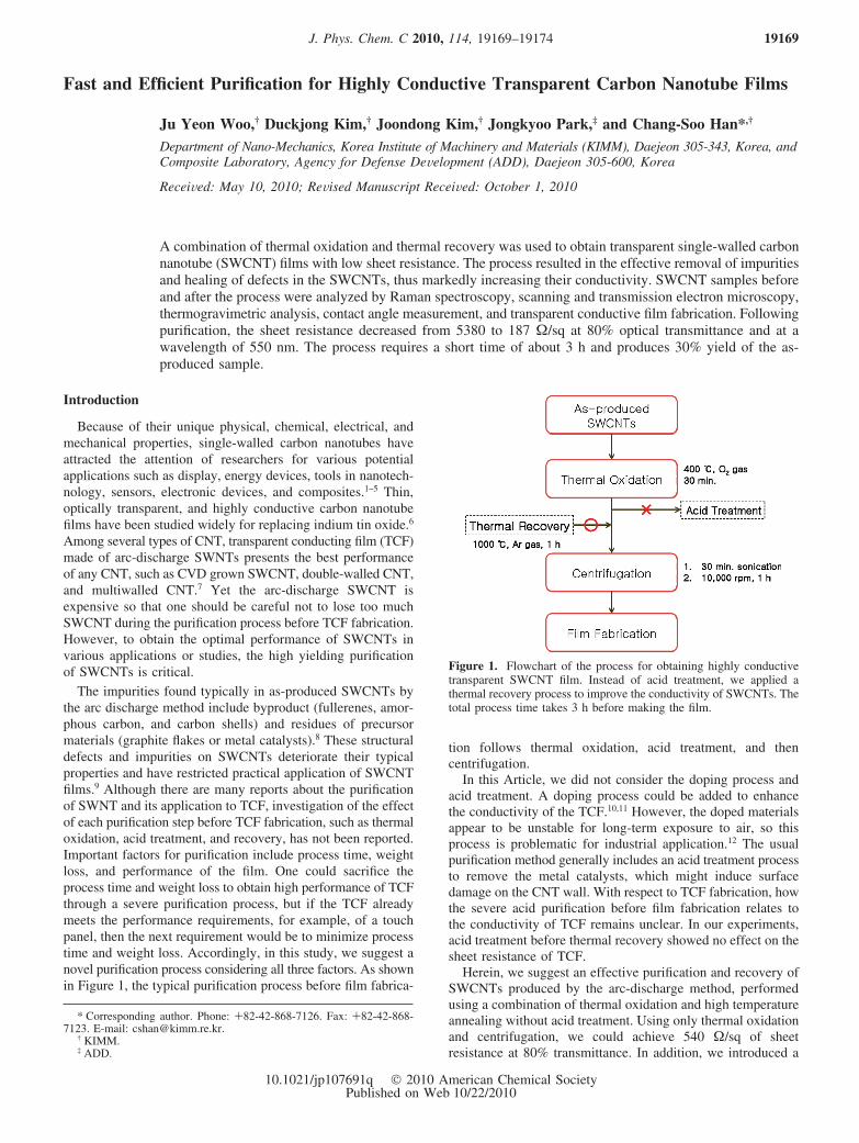
Figure 2. FE-SEM images of (a) AP, (b) TR, (c) TO, and (d) TO-TR SWCNTs. Scale bar is 500 nm.
19170 J. Phys. Chem. C, Vol. 114, No. 45, 2010 Woo et al.
ized at 550 nm using a UV-vis spectrophotometer (SD-1000,Scinco Co.). Water was dropped on the fabricated TCF film inair at room temperature using the sessile drop method. Stillimages of the droplets were captured with a CCD camera andused to measure the contact angle.
Results and Discussion
FE-SEM and TEM Characterization. Figure 2 shows theFE-SEM images of the sample of (a) AP, and after (b) TR, (c)TO, and (d) TO-TR. The images of these samples were takenin their original powder condition without dispersion andcentrifugation. As shown in Figure 2a, AP SWCNTs are coveredby numerous amorphous carbon and metal particles on theirsurfaces. From the FE-SEM images, we could hardly find pureSWCNTs because the impurities thoroughly covered theSWCNTs. However, after heat treatment, the amorphous carbonwas well removed so that many nanotubes without impuritiescould be observed (Figure 2b,c). As predicted, metal particlesremained due to the lack of chemical treatment. The structuralmorphology of TO SWNCTs appears to be straighter than thatof TR SWCNTs. During removal of amorphous carbons by theTO process, oxygen and/or small amount of water might beassociated with improving the straightness, as reported in theliterature about high-quality CNT growth.15,16 Moreover, ascompared to the image in Figure 2b, many SWCNTs withoutimpurities can be observed in Figure 2c. As for the TO process,the FE-SEM images of TO-TR SWCNTs (Figure 2d) did notdemonstrate distinct changes in terms of the impurities andstructural morphology of SWCNTs.
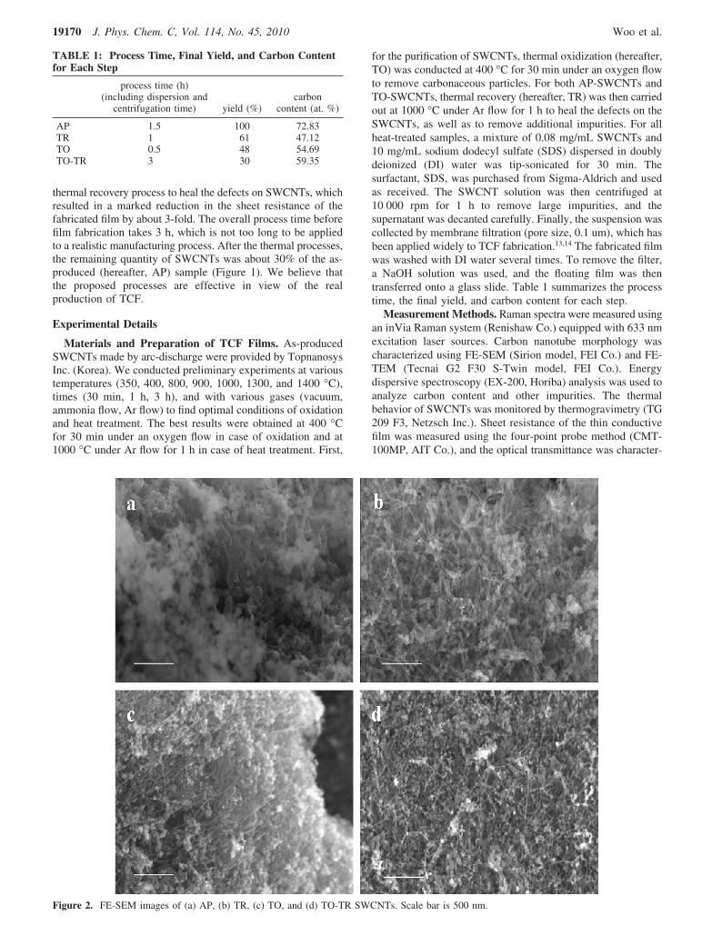
To observe the morphological variation and the structuralchanges in nanoscale after heat treatment, FE-TEM observationswere made for SWCNT samples after dispersion and centrifuga-tion. Figure 3a presents an FE-TEM image of AP SWCNTscovered by large amounts of impurities including amorphouscarbon, catalysts, and graphitic nanoparticles. As shown inFigure 3b, the FE-TEM image of only TR SWCNTs is verysimilar to that of AP SWCNT in terms of the entangled stateof the bundles, amorphous carbon, and catalyst remains. Thisindicates that the TR process alone is not sufficient to effectivelyremove the impurities from the AP sample.
In contrast, TO SWCNTs (Figure 3c) show outstandingchange with respect to the purification. Most impurities,including amorphous carbon, appear to have been removed fromthe SWCNT bundles. We can understand why thermal oxidationis an essential process for the purification of SWCNTs byremoving the amorphous carbon. Likewise, for the combinationof TO and TR (Figure 3d), the TO-TR SWCNTs display astraighter appearance in structural shape and are more uniformin diameter as compared to the other samples. SWCNTs withvery thin diameters are found at several sites in the image ofFigure 3d. One can explain that the defects on the nanotubesrecovered as the purification progressed. Note that TCF madeof straight and thin SWCNTs can achieve lower sheet resistance,as reported previously.6 The FE-TEM images demonstrate thatthe combination of TO and TR is a very effective method topurify SWCNTs, as well as to apply to TCF.
Raman Spectrum and Thermal Analysis. Figure 4 showsthe Raman spectra excited at 633 nm for the AP, TR, TO, and
Figure 3. FE-TEM images of (a) AP, (b) TR, (c) TO, and (d) TO-TR SWCNTs. Scale bar is 50 nm. The inset shows FE-TEM images with highresolution for SWCNTs, respectively. Scale bar is 10 nm.
Purification for Highly Conductive Transparent CNT Films J. Phys. Chem. C, Vol. 114, No. 45, 2010 19171
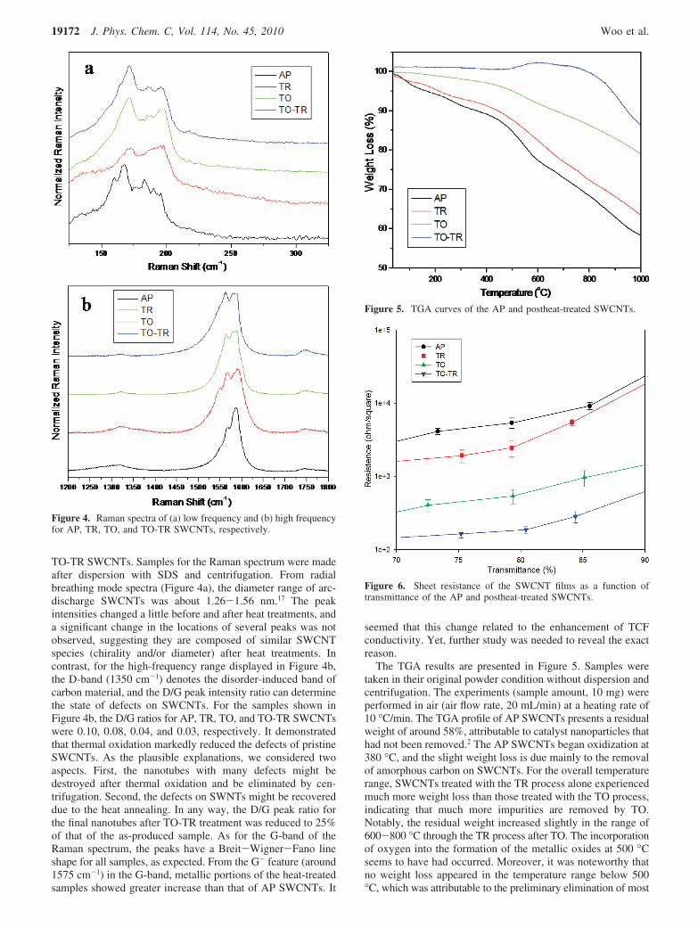
TO-TR SWCNTs. Samples for the Raman spectrum were madeafter dispersion with SDS and centrifugation. From radialbreathing mode spectra (Figure 4a), the diameter range of arc-discharge SWCNTs was about 1.26-1.56 nm.17 The peakintensities changed a little before and after heat treatments, anda significant change in the locations of several peaks was notobserved, suggesting they are composed of similar SWCNTspecies (chirality and/or diameter) after heat treatments. Incontrast, for the high-frequency range displayed in Figure 4b,the D-band (1350 cm-1) denotes the disorder-induced band ofcarbon material, and the D/G peak intensity ratio can determinethe state of defects on SWCNTs. For the samples shown inFigure 4b, the D/G ratios for AP, TR, TO, and TO-TR SWCNTswere 0.10, 0.08, 0.04, and 0.03, respectively. It demonstratedthat thermal oxidation markedly reduced the defects of pristineSWCNTs. As the plausible explanations, we considered twoaspects. First, the nanotubes with many defects might bedestroyed after thermal oxidation and be eliminated by cen-trifugation. Second, the defects on SWNTs might be recovereddue to the heat annealing. In any way, the D/G peak ratio forthe final nanotubes after TO-TR treatment was reduced to 25%of that of the as-produced sample. As for the G-band of theRaman spectrum, the peaks have a Breit-Wigner-Fano lineshape for all samples, as expected. From the G- feature (around1575 cm-1) in the G-band, metallic portions of the heat-treatedsamples showed greater increase than that of AP SWCNTs. It
seemed that this change related to the enhancement of TCFconductivity. Yet, further study was needed to reveal the exactreason.
The TGA results are presented in Figure 5. Samples weretaken in their original powder condition without dispersion andcentrifugation. The experiments (sample amount, 10 mg) wereperformed in air (air flow rate, 20 mL/min) at a heating rate of10 °C/min. The TGA profile of AP SWCNTs presents a residualweight of around 58%, attributable to catalyst nanoparticles thathad not been removed.2 The AP SWCNTs began oxidization at380 °C, and the slight weight loss is due mainly to the removalof amorphous carbon on SWCNTs. For the overall temperaturerange, SWCNTs treated with the TR process alone experiencedmuch more weight loss than those treated with the TO process,indicating that much more impurities are removed by TO.Notably, the residual weight increased slightly in the range of600-800 °C through the TR process after TO. The incorporationof oxygen into the formation of the metallic oxides at 500 °Cseems to have had occurred. Moreover, it was noteworthy thatno weight loss appeared in the temperature range below 500°C, which was attributable to the preliminary elimination of most
Figure 5. TGA curves of the AP and postheat-treated SWCNTs.
Figure 6. Sheet resistance of the SWCNT films as a function oftransmittance of the AP and postheat-treated SWCNTs.
Figure 4. Raman spectra of (a) low frequency and (b) high frequencyfor AP, TR, TO, and TO-TR SWCNTs, respectively.
19172 J. Phys. Chem. C, Vol. 114, No. 45, 2010 Woo et al.
impurities, including carbonaceous materials. The weight lossof SWCNTs after TO-TR occurred at higher temperatures thanother processes because no impurities existed to be burned away.
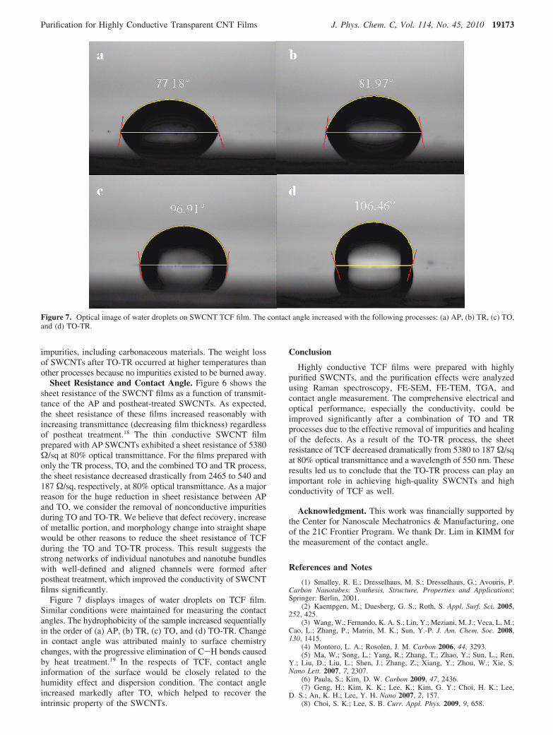
Sheet Resistance and Contact Angle. Figure 6 shows thesheet resistance of the SWCNT films as a function of transmit-tance of the AP and postheat-treated SWCNTs. As expected,the sheet resistance of these films increased reasonably withincreasing transmittance (decreasing film thickness) regardlessof postheat treatment.18 The thin conductive SWCNT filmprepared with AP SWCNTs exhibited a sheet resistance of 5380Ω/sq at 80% optical transmittance. For the films prepared withonly the TR process, TO, and the combined TO and TR process,the sheet resistance decreased drastically from 2465 to 540 and187 Ω/sq, respectively, at 80% optical transmittance. As a majorreason for the huge reduction in sheet resistance between APand TO, we consider the removal of nonconductive impuritiesduring TO and TO-TR. We believe that defect recovery, increaseof metallic portion, and morphology change into straight shapewould be other reasons to reduce the sheet resistance of TCFduring the TO and TO-TR process. This result suggests thestrong networks of individual nanotubes and nanotube bundleswith well-defined and aligned channels were formed afterpostheat treatment, which improved the conductivity of SWCNTfilms significantly.
Figure 7 displays images of water droplets on TCF film.Similar conditions were maintained for measuring the contactangles. The hydrophobicity of the sample increased sequentiallyin the order of (a) AP, (b) TR, (c) TO, and (d) TO-TR. Changein contact angle was attributed mainly to surface chemistrychanges, with the progressive elimination of C-H bonds causedby heat treatment.19 In the respects of TCF, contact angleinformation of the surface would be closely related to thehumidity effect and dispersion condition. The contact angleincreased markedly after TO, which helped to recover theintrinsic property of the SWCNTs.
Conclusion
Highly conductive TCF films were prepared with highlypurified SWCNTs, and the purification effects were analyzedusing Raman spectroscopy, FE-SEM, FE-TEM, TGA, andcontact angle measurement. The comprehensive electrical andoptical performance, especially the conductivity, could beimproved significantly after a combination of TO and TRprocesses due to the effective removal of impurities and healingof the defects. As a result of the TO-TR process, the sheetresistance of TCF decreased dramatically from 5380 to 187 Ω/sqat 80% optical transmittance and a wavelength of 550 nm. Theseresults led us to conclude that the TO-TR process can play animportant role in achieving high-quality SWCNTs and highconductivity of TCF as well.
Acknowledgment. This work was financially supported bythe Center for Nanoscale Mechatronics & Manufacturing, oneof the 21C Frontier Program. We thank Dr. Lim in KIMM forthe measurement of the contact angle.
References and Notes
(1) Smalley, R. E.; Dresselhaus, M. S.; Dresselhaus, G.; Avouris, P.Carbon Nanotubes: Synthesis, Structure, Properties and Applications;Springer: Berlin, 2001.
(2) Kaempgen, M.; Duesberg, G. S.; Roth, S. Appl. Surf. Sci. 2005,252, 425.
(3) Wang, W.; Fernando, K. A. S.; Lin, Y.; Meziani, M. J.; Veca, L. M.;Cao, L.; Zhang, P.; Matrin, M. K.; Sun, Y.-P. J. Am. Chem. Soc. 2008,130, 1415.
(4) Montoro, L. A.; Rosolen, J. M. Carbon 2006, 44, 3293.(5) Ma, W.; Song, L.; Yang, R.; Zhang, T.; Zhao, Y.; Sun, L.; Ren,
Y.; Liu, D.; Liu, L.; Shen, J.; Zhang, Z.; Xiang, Y.; Zhou, W.; Xie, S.Nano Lett. 2007, 7, 2307.
(6) Paula, S.; Kim, D. W. Carbon 2009, 47, 2436.(7) Geng, H.; Kim, K. K.; Lee, K.; Kim, G. Y.; Choi, H. K.; Lee,
D. S.; An, K. H.; Lee, Y. H. Nano 2007, 2, 157.(8) Choi, S. K.; Lee, S. B. Curr. Appl. Phys. 2009, 9, 658.
Figure 7. Optical image of water droplets on SWCNT TCF film. The contact angle increased with the following processes: (a) AP, (b) TR, (c) TO,and (d) TO-TR.
Purification for Highly Conductive Transparent CNT Films J. Phys. Chem. C, Vol. 114, No. 45, 2010 19173

(9) Gong, Q. M.; Li, Z.; Wang, Y.; Wu, B.; Zhang, Z.; Liang, J. Mater.Res. Bull. 2007, 42, 474.
(10) Bhavin, B.; Giovanni, F.; Goki, E.; Manish, C. Appl. Phys. Lett.2007, 90, 121913.
(11) Geng, H.; Kim, K. K.; So, K. P.; Lee, Y. S.; Chang, Y.; Lee, Y. H.J. Am. Chem. Soc. 2007, 129, 7758.
(12) Jackson, R.; Domercq, B.; Jain, R.; Kippelen, B.; Graham, S. AdV.Funct. Mater. 2008, 18, 2548.
(13) Tantang, H.; Ong, J. Y.; Loh, C. L.; Dong, X.; Chen, P.; Chen, Y.;Hu, X.; Tan, L. P.; Li, L.-J. Carbon 2009, 47, 1867.
(14) Wang, J.; Sun, J.; Gao, L.; Liu, Y.; Wang, Y.; Zhang, J.; Kajiura,H.; Li, Y.; Noda, K. J. Alloys Compd. 2009, 485, 456.
(15) Hata, K.; Futaba, D. H.; Mizuno, K.; Namai, T.; Ymura, M.; Iijima,S. Science 2004, 306, 1362.
(16) Zhang, G.; Mann, D.; Zhang, L.; Javey, A.; Li, Y.; Yenilmez, E.;Wang, Q.; McVittie, J. P.; Nishi, Y.; Gibbons, J.; Dai, H. Proc. Natl. Acad.Sci. U.S.A. 2005, 102, 16141.
(17) Dresselhaus, M. S.; Dresselhaus, G.; Saito, R.; Jorio, A. Phys. Rep.2005, 409, 47.
(18) Gruner, G. J. Mater. Chem. 2006, 16, 3533.(19) Mattia, D.; Rossi, M. P.; Kim, B. M.; Korneva, G.; Bau, H. H.;
Gogotsi, Y. J. Phys. Chem. B 2006, 110, 9850.
JP107691Q
19174 J. Phys. Chem. C, Vol. 114, No. 45, 2010 Woo et al.