Embed Size (px)
Citation preview
D1813HK 018-13-0061/72913HK No.A2211-1/15 Semiconductor Components Industries, LLC, 2013 December, 2013 Ver.131206YK
http://onsemi.com
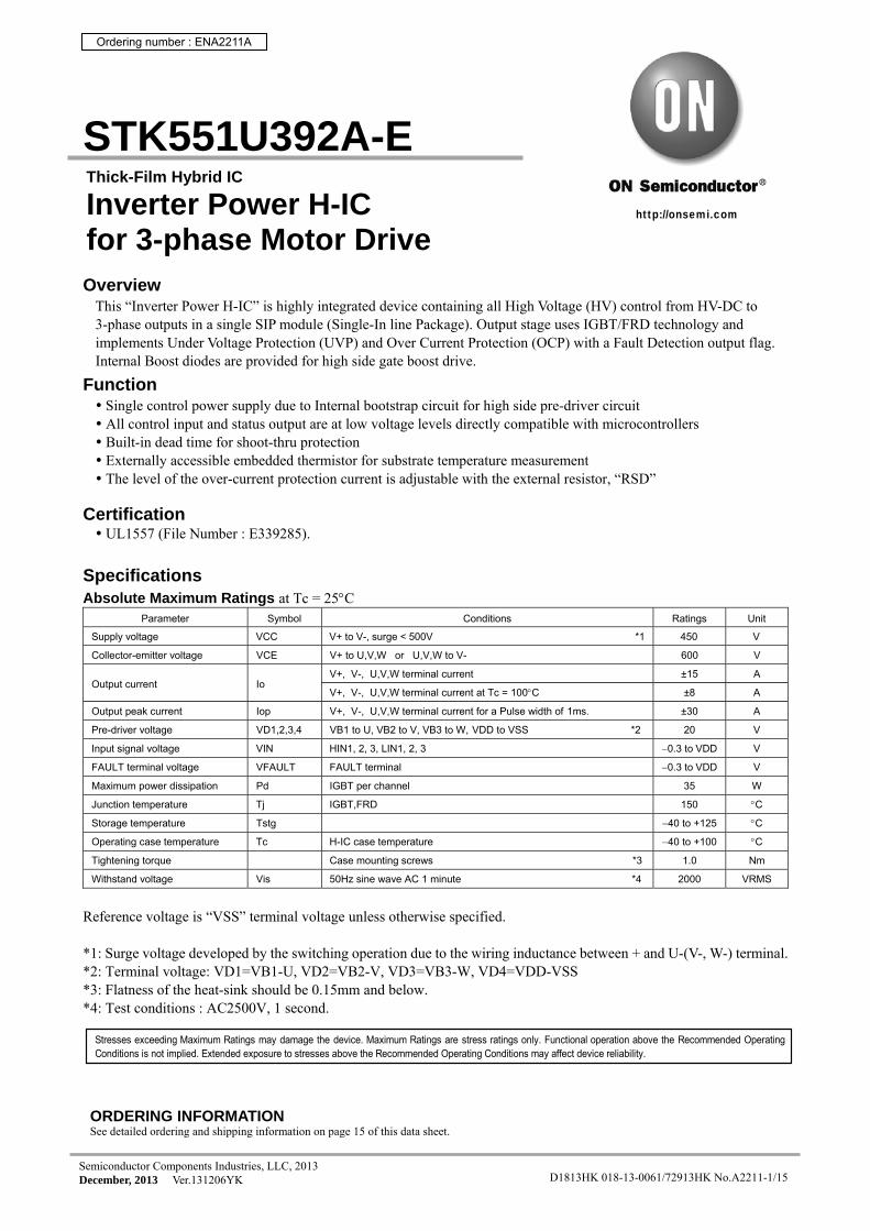
STK551U392A-E
Overview This “Inverter Power H-IC” is highly integrated device containing all High Voltage (HV) control from HV-DC to 3-phase outputs in a single SIP module (Single-In line Package). Output stage uses IGBT/FRD technology and implements Under Voltage Protection (UVP) and Over Current Protection (OCP) with a Fault Detection output flag. Internal Boost diodes are provided for high side gate boost drive.
Function Single control power supply due to Internal bootstrap circuit for high side pre-driver circuit All control input and status output are at low voltage levels directly compatible with microcontrollers Built-in dead time for shoot-thru protection Externally accessible embedded thermistor for substrate temperature measurement The level of the over-current protection current is adjustable with the external resistor, “RSD”
Certification UL1557 (File Number : E339285).
Specifications Absolute Maximum Ratings at Tc = 25C
Parameter Symbol Conditions Ratings Unit
Supply voltage VCC V+ to V-, surge < 500V *1 450 V
Collector-emitter voltage VCE V+ to U,V,W or U,V,W to V- 600 V
Output current Io V+, V-, U,V,W terminal current ±15 A
V+, V-, U,V,W terminal current at Tc = 100C ±8 A
Output peak current Iop V+, V-, U,V,W terminal current for a Pulse width of 1ms. ±30 A
Pre-driver voltage VD1,2,3,4 VB1 to U, VB2 to V, VB3 to W, VDD to VSS *2 20 V
Input signal voltage VIN HIN1, 2, 3, LIN1, 2, 3 0.3 to VDD V
FAULT terminal voltage VFAULT FAULT terminal 0.3 to VDD V
Maximum power dissipation Pd IGBT per channel 35 W
Junction temperature Tj IGBT,FRD 150 C
Storage temperature Tstg 40 to +125 C
Operating case temperature Tc H-IC case temperature 40 to +100 C
Tightening torque Case mounting screws *3 1.0 Nm
Withstand voltage Vis 50Hz sine wave AC 1 minute *4 2000 VRMS
Reference voltage is “VSS” terminal voltage unless otherwise specified. *1: Surge voltage developed by the switching operation due to the wiring inductance between + and U-(V-, W-) terminal. *2: Terminal voltage: VD1=VB1-U, VD2=VB2-V, VD3=VB3-W, VD4=VDD-VSS *3: Flatness of the heat-sink should be 0.15mm and below. *4: Test conditions : AC2500V, 1 second.
Thick-Film Hybrid IC
Inverter Power H-IC for 3-phase Motor Drive
Stresses exceeding Maximum Ratings may damage the device. Maximum Ratings are stress ratings only. Functional operation above the Recommended OperatingConditions is not implied. Extended exposure to stresses above the Recommended Operating Conditions may affect device reliability.
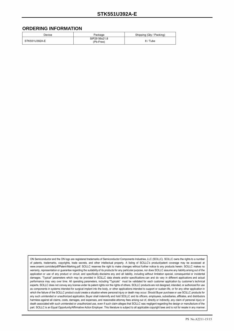
ORDERING INFORMATION See detailed ordering and shipping information on page 15 of this data sheet.
Ordering number : ENA2211A
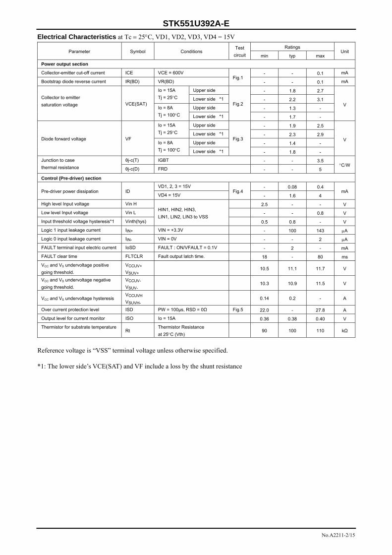
STK551U392A-E
No.A2211-2/15
Electrical Characteristics at Tc 25C, VD1, VD2, VD3, VD4 = 15V
Parameter Symbol Conditions Test
circuit
Ratings Unit
min typ max
Power output section
Collector-emitter cut-off current ICE VCE = 600V Fig.1
- - 0.1 mA
Bootstrap diode reverse current IR(BD) VR(BD) - - 0.1 mA
Collector to emitter
saturation voltage VCE(SAT)
Io = 15A
Tj = 25C
Upper side
Fig.2
- 1.8 2.7
V Lower side *1 - 2.2 3.1
Io = 8A
Tj = 100C
Upper side - 1.3 -
Lower side *1 - 1.7 -
Diode forward voltage VF
Io = 15A
Tj = 25C
Upper side
Fig.3
- 1.9 2.5
V Lower side *1 - 2.3 2.9
Io = 8A
Tj = 100C
Upper side - 1.4 -
Lower side *1 - 1.8 -
Junction to case
thermal resistance
θj-c(T) IGBT - - 3.5 C/W
θj-c(D) FRD - - 5
Control (Pre-driver) section
Pre-driver power dissipation ID VD1, 2, 3 = 15V
Fig.4 - 0.08 0.4
mA VD4 = 15V - 1.6 4
High level Input voltage Vin H HIN1, HIN2, HIN3,
LIN1, LIN2, LIN3 to VSS
2.5 - - V
Low level Input voltage Vin L - - 0.8 V
Input threshold voltage hysteresis*1 Vinth(hys) 0.5 0.8 - V
Logic 1 input leakage current IIN+ VIN = +3.3V - 100 143 A
Logic 0 input leakage current IIN- VIN = 0V - - 2 A
FAULT terminal input electric current IoSD FAULT : ON/VFAULT = 0.1V - 2 - mA
FAULT clear time FLTCLR Fault output latch time. 18 - 80 ms
VCC and VS undervoltage positive
going threshold.
VCCUV+
VSUV+
10.5 11.1 11.7 V
VCC and VS undervoltage negative
going threshold.
VCCUV-
VSUV-
10.3 10.9 11.5 V
VCC and VS undervoltage hysteresis VCCUVH
VSUVH-
0.14 0.2 - A
Over current protection level ISD PW = 100μs, RSD = 0Ω Fig.5 22.0 - 27.8 A
Output level for current monitor ISO Io = 15A 0.36 0.38 0.40 V
Thermistor for substrate temperatureRt
Thermistor Resistance
at 25C (Vth)
90 100 110 kΩ
Reference voltage is “VSS” terminal voltage unless otherwise specified. *1: The lower side’s VCE(SAT) and VF include a loss by the shunt resistance
STK551U392A-E
No.A2211-3/15
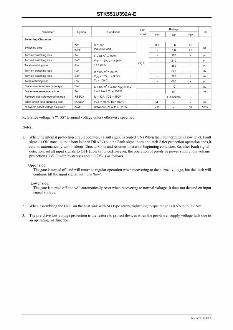
Parameter Symbol Conditions Test
circuit
Ratings Unit
min typ max
Switching Character
Switching time tON Io = 15A
Inductive load
Fig.6
0.3 0.6 1.3 s
tOFF - 1.0 1.8
Turn-on switching loss Eon Ic = 8A,V+
= 300V,
VDD = 15V, L = 3.9mH
Tc = 25C
- 170 - J
Turn-off switching loss Eoff - 210 - J
Total switching loss Etot - 380 - J
Turn-on switching loss Eon Ic = 8A, V+ = 300 V,
VDD = 15V, L = 3.9mH
Tc = 100C
- 220 - J
Turn-off switching loss Eoff - 380 - J
Total switching loss Etot - 600 - J
Diode reverse recovery energy Erec IF = 8A, V+
= 400V, VDD = 15V,
L = 3.9mH, Tc = 100C
- 12 - J
Diode reverse recovery time Trr - 54 - ns
Reverse bias safe operating area RBSOA Io = 30A, VCE = 450V Full square
Short circuit safe operating area SCSOA VCE = 400V, Tc = 100C 4 - - s
Allowable offset voltage slew rate dv/dt Between U,V,W to U-,V-,W- 50 - 50 V/ns
Reference voltage is “VSS” terminal voltage unless otherwise specified. Notes: 1. When the internal protection circuit operates, a Fault signal is turned ON (When the Fault terminal is low level, Fault
signal is ON state : output form is open DRAIN) but the Fault signal does not latch.After protection operation ends,it returns automatically within about 18ms to 80ms and resumes operation beginning condition. So, after Fault signal detection, set all input signals to OFF (Low) at once.However, the operation of pre-drive power supply low voltage protection (UVLO:with hysteresis about 0.2V) is as follows.
Upper side:
The gate is turned off and will return to regular operation when recovering to the normal voltage, but the latch will continue till the input signal will turn ‘low’.
Lower side: The gate is turned off and will automatically reset when recovering to normal voltage. It does not depend on input signal voltage.
2. When assembling the H-IC on the heat sink with M3 type screw, tightening torque range is 0.6 Nm to 0.9 Nm.
3. The pre-drive low voltage protection is the feature to protect devices when the pre-driver supply voltage falls due to an operating malfunction.
STK551U392A-E
No.A2211-4/15
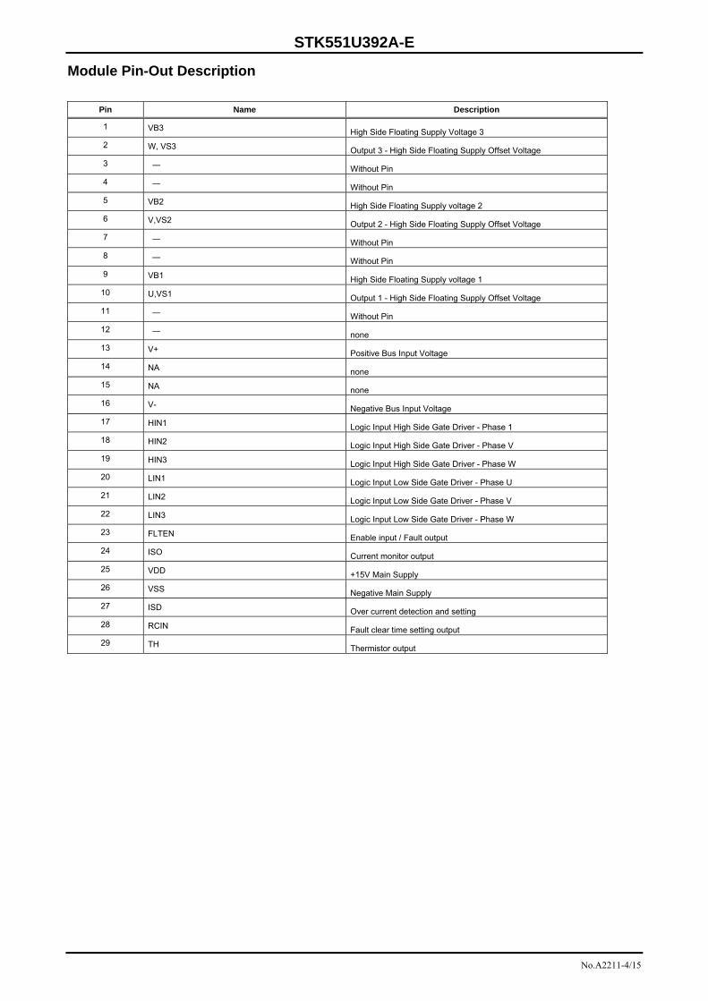
Module Pin-Out Description
Pin Name Description
1 VB3 High Side Floating Supply Voltage 3
2 W, VS3 Output 3 - High Side Floating Supply Offset Voltage
3 ― Without Pin
4 ― Without Pin
5 VB2 High Side Floating Supply voltage 2
6 V,VS2 Output 2 - High Side Floating Supply Offset Voltage
7 ― Without Pin
8 ― Without Pin
9 VB1 High Side Floating Supply voltage 1
10 U,VS1 Output 1 - High Side Floating Supply Offset Voltage
11 ― Without Pin
12 ― none
13 V+ Positive Bus Input Voltage
14 NA none
15 NA none
16 V- Negative Bus Input Voltage
17 HIN1 Logic Input High Side Gate Driver - Phase 1
18 HIN2 Logic Input High Side Gate Driver - Phase V
19 HIN3 Logic Input High Side Gate Driver - Phase W
20 LIN1 Logic Input Low Side Gate Driver - Phase U
21 LIN2 Logic Input Low Side Gate Driver - Phase V
22 LIN3 Logic Input Low Side Gate Driver - Phase W
23 FLTEN Enable input / Fault output
24 ISO Current monitor output
25 VDD +15V Main Supply
26 VSS Negative Main Supply
27 ISD Over current detection and setting
28 RCIN Fault clear time setting output
29 TH Thermistor output
STK551U392A-E
No.A2211-5/15
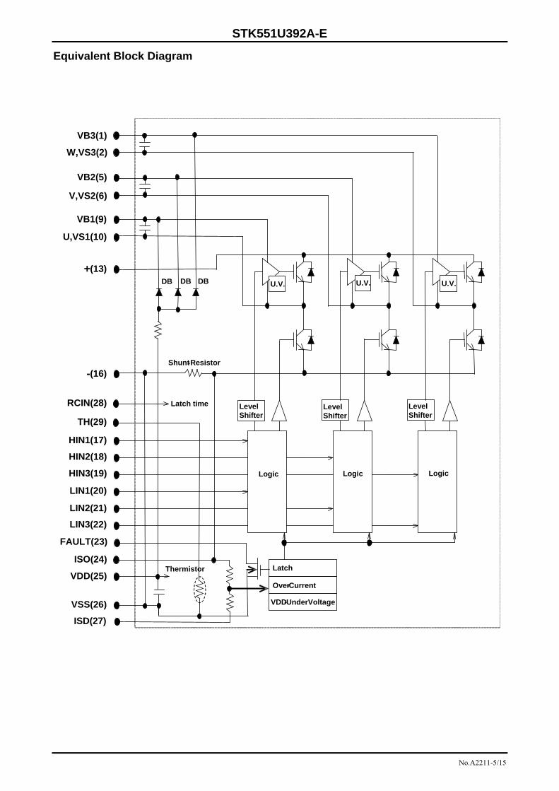
Equivalent Block Diagram
+(13)
HIN1(17)
HIN2(18)
HIN3(19)
LIN1(20)
LIN2(21)
LIN3(22)
FAULT(23)
ISO(24)
VDD(25)
VSS(26)
ISD(27)
Shunt - Resistor
Level Shifter
Level Shifter
Level Shifter
Latch time
Logic Logic Logic
VDD-UnderVoltage
Thermistor
V,VS2(6)
VB1(9)
U,VS1(10)
-(16)
TH(29)
RCIN(28)
VB3(1)
W,VS3(2)
VB2(5)
U.V. U.V. U.V.
Latch
DB DB DB
Over-Current
STK551U392A-E
No.A2211-6/15
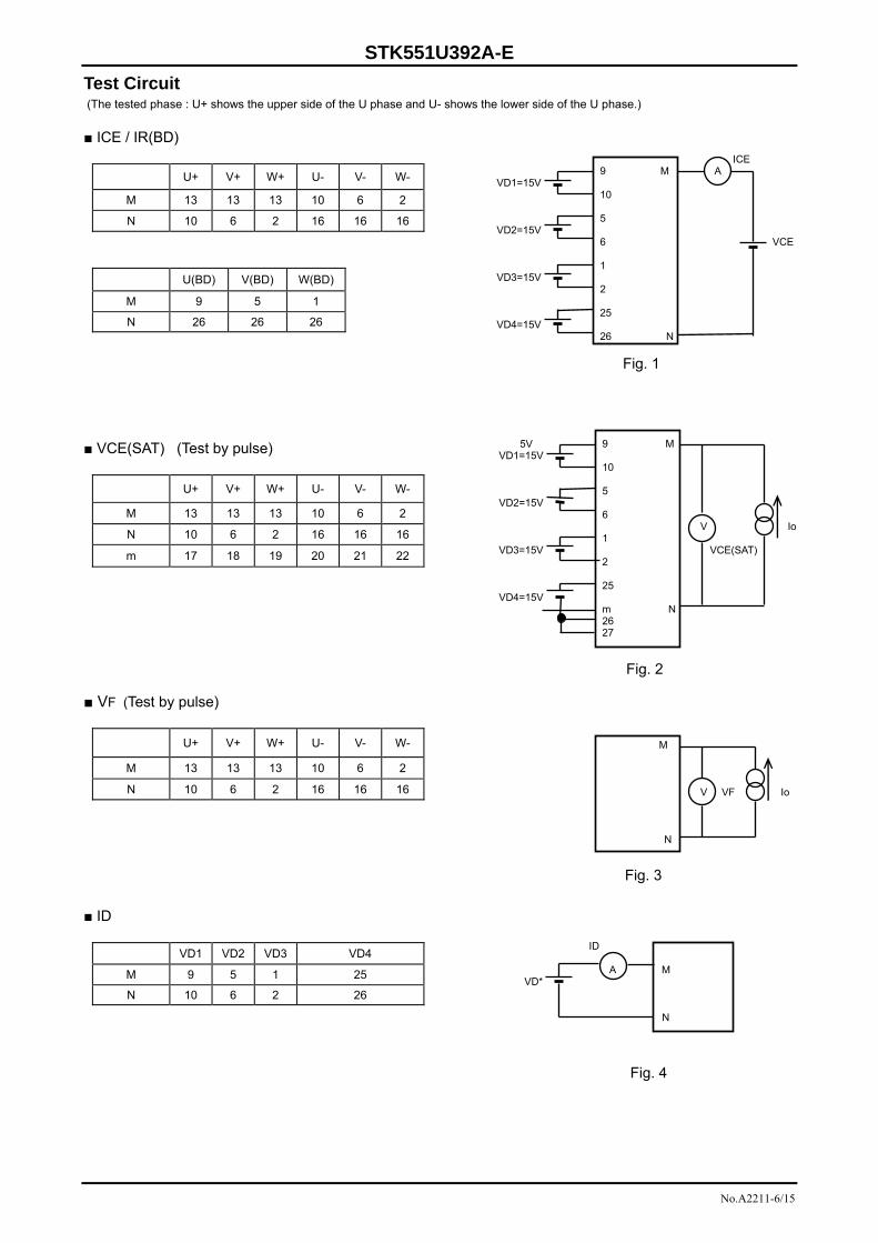
Test Circuit (The tested phase : U+ shows the upper side of the U phase and U- shows the lower side of the U phase.)
ICE / IR(BD)
U+ V+ W+ U- V- W-
M 13 13 13 10 6 2
N 10 6 2 16 16 16
U(BD) V(BD) W(BD)
M 9 5 1
N 26 26 26
VCE(SAT) (Test by pulse)
U+ V+ W+ U- V- W-
M 13 13 13 10 6 2
N 10 6 2 16 16 16
m 17 18 19 20 21 22
VF (Test by pulse)
U+ V+ W+ U- V- W-
M 13 13 13 10 6 2
N 10 6 2 16 16 16
ID
VD1 VD2 VD3 VD4
M 9 5 1 25
N 10 6 2 26
ICE 9 M A
VD1=15V 10
5
VD2=15V 6 VCE
1
VD3=15V 2
25
VD4=15V 26 N
9 M VD1=15V
10
5 VD2=15V
6 V Io
1 VD3=15V VCE(SAT)
2
25 VD4=15V
m N 26 27
M
V VF Io
N
ID
A M VD*
N
Fig. 1
Fig. 4
5V
Fig. 2
Fig. 3
STK551U392A-E
No.A2211-7/15
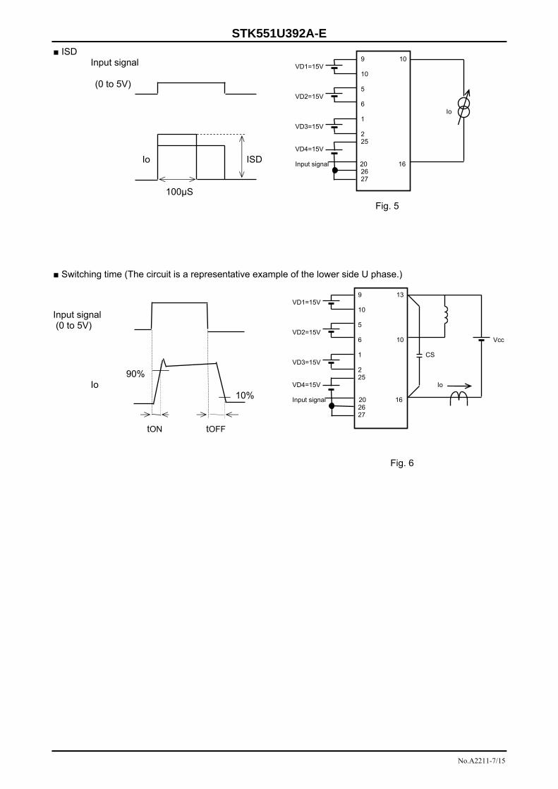
ISD Input signal (0 to 5V)
Io ISD
100μS
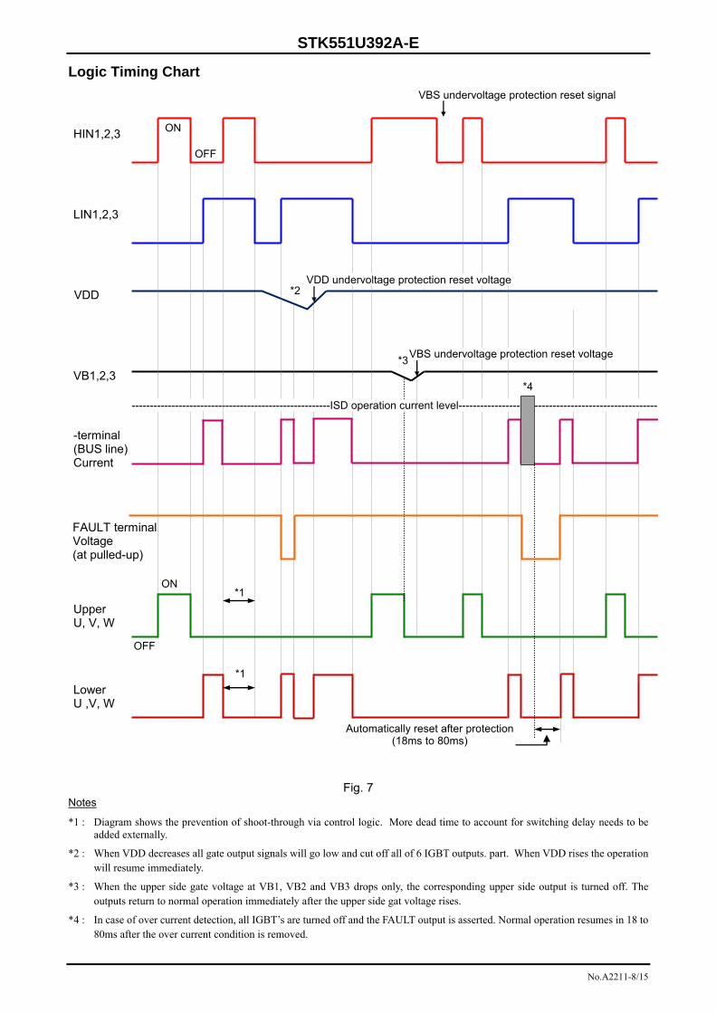
Switching time (The circuit is a representative example of the lower side U phase.)
Input signal (0 to 5V)
90%
Io 10%
tON tOFF
9 10
VD1=15V 10
5
VD2=15V 6
Io 1
VD3=15V 2 25
VD4=15V Input signal 20 16
26 27
9 13 VD1=15V
10
5 VD2=15V
6 10 Vcc
1 CS VD3=15V
2 25
VD4=15V Io Input signal 20 16
26 27
Fig. 6
Fig. 5
STK551U392A-E
No.A2211-8/15
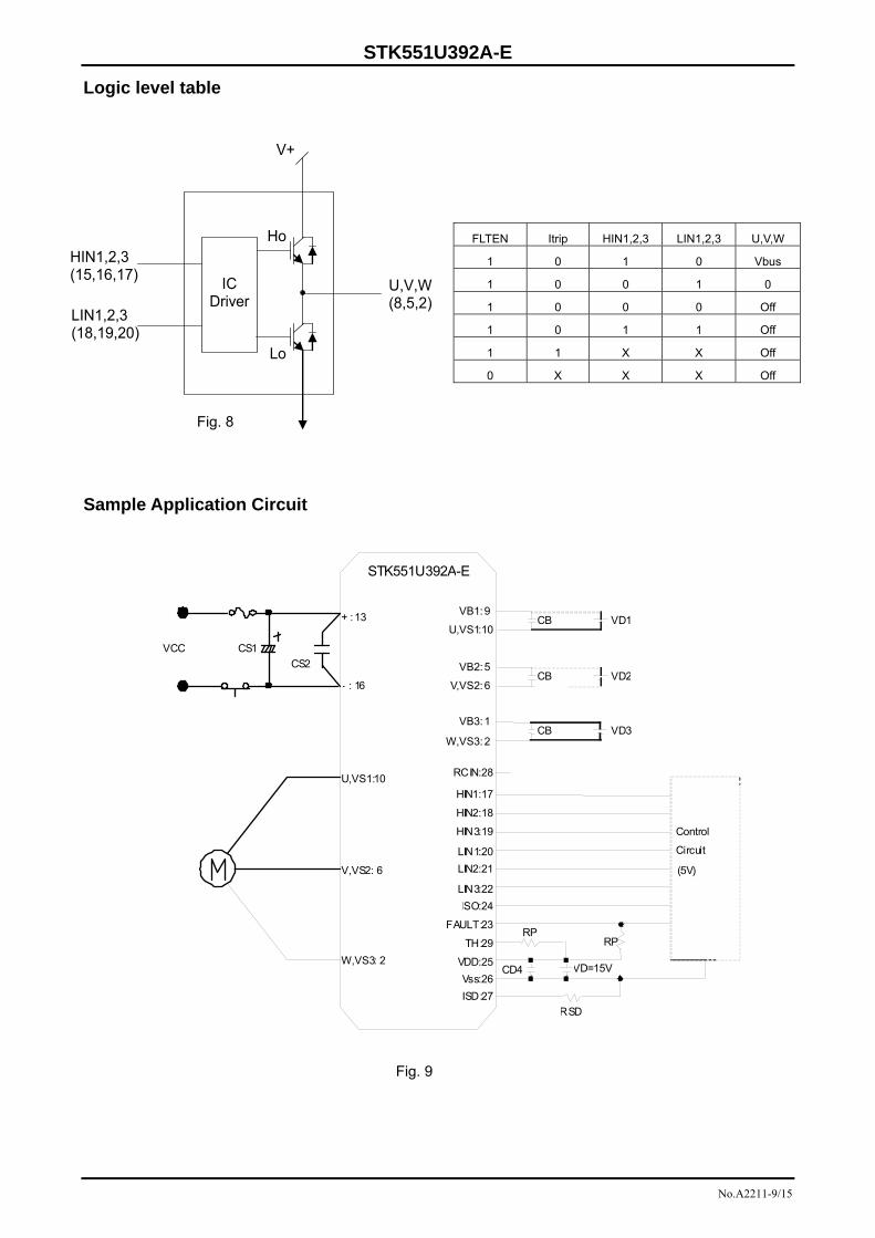
Logic Timing Chart
Fig. 7 Notes
*1 : Diagram shows the prevention of shoot-through via control logic. More dead time to account for switching delay needs to be added externally.
*2 : When VDD decreases all gate output signals will go low and cut off all of 6 IGBT outputs. part. When VDD rises the operation will resume immediately.
*3 : When the upper side gate voltage at VB1, VB2 and VB3 drops only, the corresponding upper side output is turned off. The outputs return to normal operation immediately after the upper side gat voltage rises.
*4 : In case of over current detection, all IGBT’s are turned off and the FAULT output is asserted. Normal operation resumes in 18 to 80ms after the over current condition is removed.
ON
OFF
HIN1,2,3
LIN1,2,3
-terminal (BUS line) Current
Upper U, V, W
Lower U ,V, W
VB1,2,3
*1
*1
OFF
ON
*2
*3
VBS undervoltage protection reset signal
VDD undervoltage protection reset voltage
-------------------------------------------------------ISD operation current level-------------------------------------------------------
Automatically reset after protection (18ms to 80ms)
*4
VDD
VBS undervoltage protection reset voltage
FAULT terminal Voltage (at pulled-up)
STK551U392A-E
No.A2211-9/15
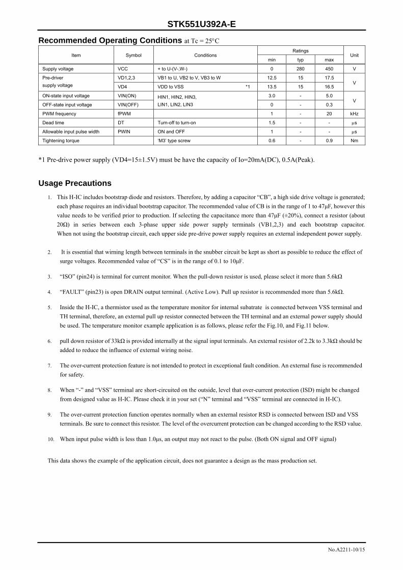
Logic level table
Sample Application Circuit
VB1: 9+ : 13
U,VS1:10
- : 16
LIN2:21
LIN3:22
ISO:24
FAULT:23
VDD:25
Vss:26VD=15V
STK551U392A-E
CS2
CS1
ISD:27
RP
LIN1:20
HIN2:18
HIN3:19
HIN1:17
VB2: 5
V,VS2: 6
VB3: 1
W,VS3: 2
U,VS1:10
V,VS2: 6
W,VS3: 2
TH:29RP
RCIN:28
VCC
CB VD1
VD2
CB
CB
VD3
Control
Circuit
(5V)
CD4
RSD
FLTEN Itrip HIN1,2,3 LIN1,2,3 U,V,W
1 0 1 0 Vbus
1 0 0 1 0
1 0 0 0 Off
1 0 1 1 Off
1 1 X X Off
0 X X X Off
HoHIN1,2,3 (15,16,17)
IC Driver
Lo
LIN1,2,3 (18,19,20)
V+
U,V,W(8,5,2)
Fig. 8
Fig. 9
STK551U392A-E
No.A2211-10/15
Recommended Operating Conditions at Tc = 25C
Item Symbol Conditions Ratings
Unit min typ max
Supply voltage VCC + to U-(V-,W-) 0 280 450 V
Pre-driver
supply voltage
VD1,2,3 VB1 to U, VB2 to V, VB3 to W 12.5 15 17.5 V
VD4 VDD to VSS *1 13.5 15 16.5
ON-state input voltage VIN(ON) HIN1, HIN2, HIN3, LIN1, LIN2, LIN3
3.0 - 5.0 V
OFF-state input voltage VIN(OFF) 0 - 0.3
PWM frequency fPWM 1 - 20 kHz
Dead time DT Turn-off to turn-on 1.5 - - s
Allowable input pulse width PWIN ON and OFF 1 - - s
Tightening torque ‘M3’ type screw 0.6 - 0.9 Nm
*1 Pre-drive power supply (VD4=15±1.5V) must be have the capacity of Io=20mA(DC), 0.5A(Peak).
Usage Precautions
1. This H-IC includes bootstrap diode and resistors. Therefore, by adding a capacitor “CB”, a high side drive voltage is generated;
each phase requires an individual bootstrap capacitor. The recommended value of CB is in the range of 1 to 47μF, however this
value needs to be verified prior to production. If selecting the capacitance more than 47μF (±20%), connect a resistor (about
20Ω) in series between each 3-phase upper side power supply terminals (VB1,2,3) and each bootstrap capacitor.
When not using the bootstrap circuit, each upper side pre-drive power supply requires an external independent power supply.
2. It is essential that wirning length between terminals in the snubber circuit be kept as short as possible to reduce the effect of
surge voltages. Recommended value of “CS” is in the range of 0.1 to 10μF.
3. “ISO” (pin24) is terminal for current monitor. When the pull-down resistor is used, please select it more than 5.6kΩ
4. “FAULT” (pin23) is open DRAIN output terminal. (Active Low). Pull up resistor is recommended more than 5.6kΩ.
5. Inside the H-IC, a thermistor used as the temperature monitor for internal subatrate is connected between VSS terminal and
TH terminal, therefore, an external pull up resistor connected between the TH terminal and an external power supply should
be used. The temperature monitor example application is as follows, please refer the Fig.10, and Fig.11 below.
6. pull down resistor of 33kΩ is provided internally at the signal input terminals. An external resistor of 2.2k to 3.3kΩ should be
added to reduce the influence of external wiring noise.
7. The over-current protection feature is not intended to protect in exceptional fault condition. An external fuse is recommended
for safety.
8. When “-” and “VSS” terminal are short-circuited on the outside, level that over-current protection (ISD) might be changed
from designed value as H-IC. Please check it in your set (“N” terminal and “VSS” terminal are connected in H-IC).
9. The over-current protection function operates normally when an external resistor RSD is connected between ISD and VSS
terminals. Be sure to connect this resistor. The level of the overcurrent protection can be changed according to the RSD value.
10. When input pulse width is less than 1.0μs, an output may not react to the pulse. (Both ON signal and OFF signal)
This data shows the example of the application circuit, does not guarantee a design as the mass production set.
STK551U392A-E
No.A2211-11/15
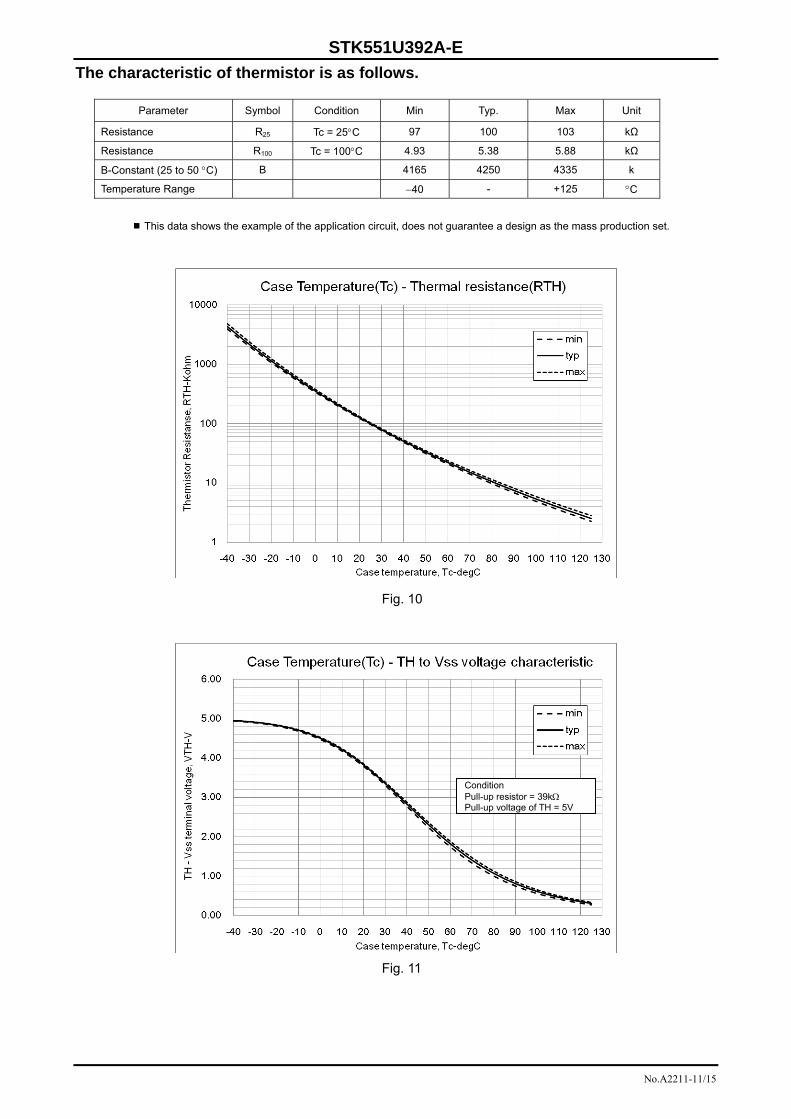
The characteristic of thermistor is as follows.
Parameter Symbol Condition Min Typ. Max Unit
Resistance R25 Tc = 25C 97 100 103 kΩ
Resistance R100 Tc = 100C 4.93 5.38 5.88 kΩ
B-Constant (25 to 50 C) B 4165 4250 4335 k
Temperature Range 40 - +125 C
This data shows the example of the application circuit, does not guarantee a design as the mass production set.
Condition Pull-up resistor = 39k Pull-up voltage of TH = 5V
Fig. 10
Fig. 11
STK551U392A-E
No.A2211-12/15
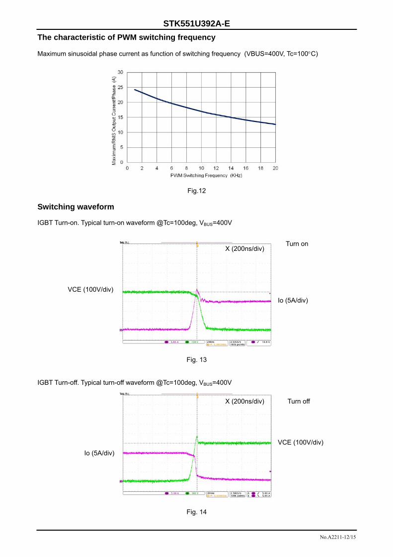
The characteristic of PWM switching frequency Maximum sinusoidal phase current as function of switching frequency (VBUS=400V, Tc=100C)
Fig.12 Switching waveform IGBT Turn-on. Typical turn-on waveform @Tc=100deg, VBUS=400V
Fig. 13 IGBT Turn-off. Typical turn-off waveform @Tc=100deg, VBUS=400V
Fig. 14
VCE (100V/div)
Io (5A/div)
X (200ns/div)
VCE (100V/div)
Io (5A/div)
X (200ns/div)
Turn on
Turn off
STK551U392A-E
No.A2211-13/15
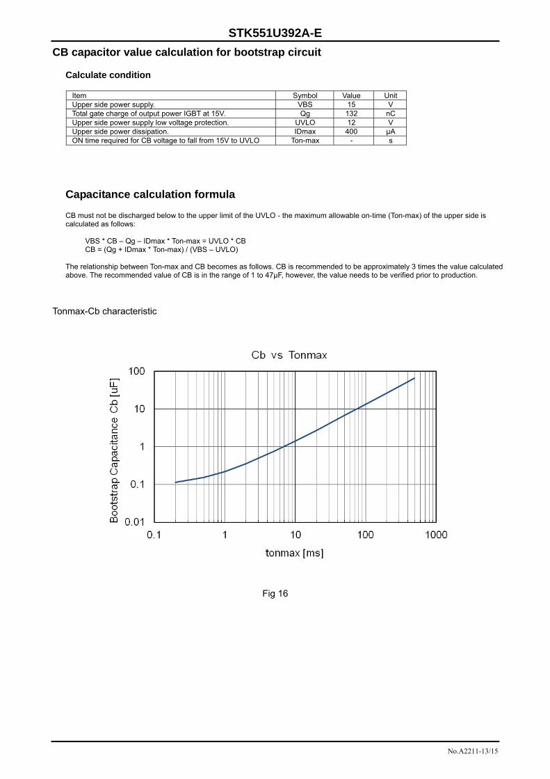
CB capacitor value calculation for bootstrap circuit
Calculate condition
Item Symbol Value Unit Upper side power supply. VBS 15 V Total gate charge of output power IGBT at 15V. Qg 132 nC Upper side power supply low voltage protection. UVLO 12 V Upper side power dissipation. IDmax 400 μA ON time required for CB voltage to fall from 15V to UVLO Ton-max - s
Capacitance calculation formula CB must not be discharged below to the upper limit of the UVLO - the maximum allowable on-time (Ton-max) of the upper side is calculated as follows:
VBS * CB – Qg – IDmax * Ton-max = UVLO * CB CB = (Qg + IDmax * Ton-max) / (VBS – UVLO)
The relationship between Ton-max and CB becomes as follows. CB is recommended to be approximately 3 times the value calculated above. The recommended value of CB is in the range of 1 to 47μF, however, the value needs to be verified prior to production.
Tonmax-Cb characteristic
Fig 16
STK551U392A-E
No.A2211-14/15
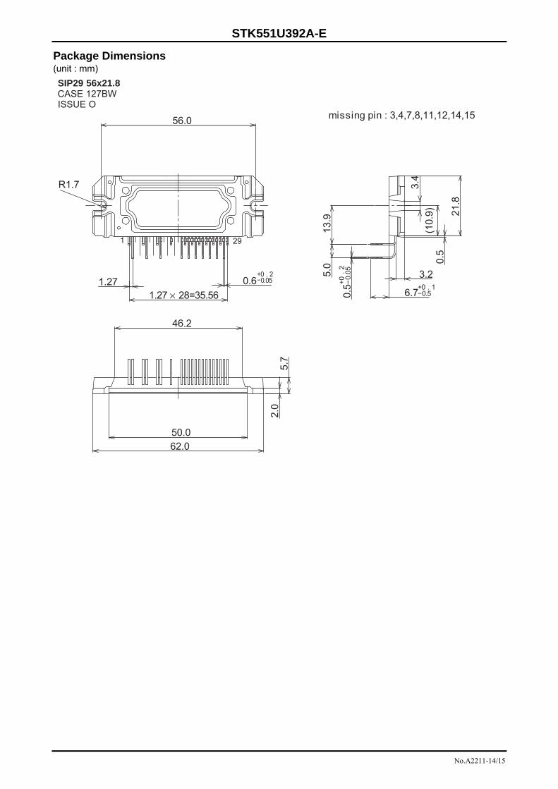
Package Dimensions (unit : mm)
SIP29 56x21.8CASE 127BWISSUE O
missing pin : 3,4,7,8,11,12,14,1556.0
1 29
62.0
5.7
2.0
46.2
50.0
1.271.27 × 28=35.56
0.6+0 . 2−0.05
3.4
0.5
21.8
13.9
5.0
0.5+
0.
2−
0.05 3.2
6.7+0 . 1−0.5
(10.
9)
R1.7
STK551U392A-E
No.A2211-15/15
ORDERING INFORMATION Device Package Shipping (Qty / Packing)
STK551U392A-E SIP29 56x21.8
(Pb-Free) 8 / Tube
ON Semiconductor and the ON logo are registered trademarks of Semiconductor Components Industries, LLC (SCILLC). SCILLC owns the rights to a numberof patents, trademarks, copyrights, trade secrets, and other intellectual property. A listing of SCILLC’s product/patent coverage may be accessed atwww.onsemi.com/site/pdf/Patent-Marking.pdf. SCILLC reserves the right to make changes without further notice to any products herein. SCILLC makes nowarranty, representation or guarantee regarding the suitability of its products for any particular purpose, nor does SCILLC assume any liability arising out of theapplication or use of any product or circuit, and specifically disclaims any and all liability, including without limitation special, consequential or incidentaldamages. “Typical” parameters which may be provided in SCILLC data sheets and/or specifications can and do vary in different applications and actualperformance may vary over time. All operating parameters, including “Typicals” must be validated for each customer application by customer’s technicalexperts. SCILLC does not convey any license under its patent rights nor the rights of others. SCILLC products are not designed, intended, or authorized for useas components in systems intended for surgical implant into the body, or other applications intended to support or sustain life, or for any other application inwhich the failure of the SCILLC product could create a situation where personal injury or death may occur. Should Buyer purchase or use SCILLC products forany such unintended or unauthorized application, Buyer shall indemnify and hold SCILLC and its officers, employees, subsidiaries, affiliates, and distributorsharmless against all claims, costs, damages, and expenses, and reasonable attorney fees arising out of, directly or indirectly, any claim of personal injury ordeath associated with such unintended or unauthorized use, even if such claim alleges that SCILLC was negligent regarding the design or manufacture of thepart. SCILLC is an Equal Opportunity/Affirmative Action Employer. This literature is subject to all applicable copyright laws and is not for resale in any manner.
PS


![PMXU43BT • PMXU63BT • PMXU83BT USER’S MANUAL...1. The external power input socket, receiving external power supply, DC +15V, -15V, +48V, ground wire 2. Power Switch [PROGRAM]](https://img.pdfslide.us/doc/110x75/6118f81456c78877893ef51d/pmxu43bt-a-pmxu63bt-a-pmxu83bt-useras-manual-1-the-external-power-input.jpg)