Embed Size (px)
Citation preview
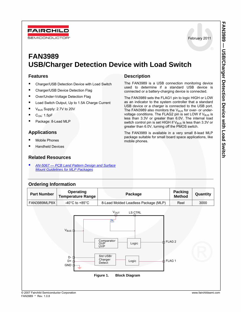
February 2011
© 2007 Fairchild Semiconductor Corporation www.fairchildsemi.com FAN3989 Rev. 1.0.8
FA
N3989 —
US
B/C
harg
er Detectio
n D
evice with
Lo
ad S
witch
FAN3989 USB/Charger Detection Device with Load Switch
Features
Charger/USB Detection Device with Load Switch
Charger/USB Device Detection Flag
Over/Under-Voltage Detection Flag
Load Switch Output, Up to 1.5A Charge Current
VBUS Supply: 2.7V to 20V
CON: 1.5pF
Package: 8-Lead MLP
Applications
Mobile Phones
Handheld Devices
Related Resources
AN-5067 — PCB Land Pattern Design and Surface Mount Guidelines for MLP Packages
Description
The FAN3989 is a USB connection monitoring device used to determine if a standard USB device is connected or a battery-charging device is connected.
The FAN3989 sets the FLAG1 pin to logic HIGH or LOW as an indicator to the system controller that a standard USB device or a charger is connected to the USB port. The FAN3989 also monitors the VBUS for over- or under-voltage conditions. The FLAG2 pin is set LOW if VBUS is less than 3.3V or greater than 6.0V. The internal load switch control pin is set HIGH if VBUS is less than 3.3V or greater than 6.0V, turning off the PMOS switch.
The FAN3989 is available in a very small 8-lead MLP package suitable for small board space applications, like mobile phones.
Ordering Information
Part Number Operating
Temperature Range Package
Packing Method
Quantity
FAN3989MLP8X -40°C to +85°C 8-Lead Molded Leadless Package (MLP) Reel 3000
Std USB/ChargerDetect
LogicD+
VOUT
Logic
LS CTRL
FLAG 1
FLAG 2
GND
D-
ComparatorOVPUVP
VBUS
Figure 1. Block Diagram

© 2007 Fairchild Semiconductor Corporation www.fairchildsemi.com FAN3989 • Rev. 1.0.8 2
FA
N3989 —
US
B/C
harg
er Detectio
n D
evice with
Lo
ad S
witch
Pin Configuration
Figure 2. Pin Configuration (Top View) Figure 3. Pin Configuration (Bottom View)
Pin Definitions
Pin# Name Type Description
1 D+ Input USB Data Input
2 GND Input Device Ground
3 Flag2 Output Over-/Under-Voltage Flag Output
4 LSCTRL Output PMOS Switch Control – Pull-Up Connection to VBUS
5 VOUT Output Voltage Out – Connection also on Package DAP (see PCB Layout Guideline section)
6 VBUS Input Power Input from Charger, USB Device, or Handheld Battery
7 Flag1 Output Charger / Standard USB Device Detect Flag
8 D- Input USB Data Input
Truth Table
Connection State
VBUS D- D+ FLAG1 FLAG2LS
CTRL Description
STD USB Device 0V R to GND R to VDD LOW LOW HIGH Load switch open
STD USB Device 5V R to GND R to VDD LOW HIGH LOW Load switch closed
USB Charger 5V Short to D+ Short to D- HIGH HIGH LOW Normal state, load switch closed
VBUS GT 6V GT 6V Short to D+ Short to D- HIGH LOW HIGH Load switch open
VBUS LT 3.3V LT 3.3V Short to D+ Short to D- HIGH LOW HIGH Load switch open
PC Charger 5V Open Open LOW HIGH LOW Load switch closed
© 2007 Fairchild Semiconductor Corporation www.fairchildsemi.com FAN3989 • Rev. 1.0.8 3
FA
N3989 —
US
B/C
harg
er Detectio
n D
evice with
Lo
ad S
witch
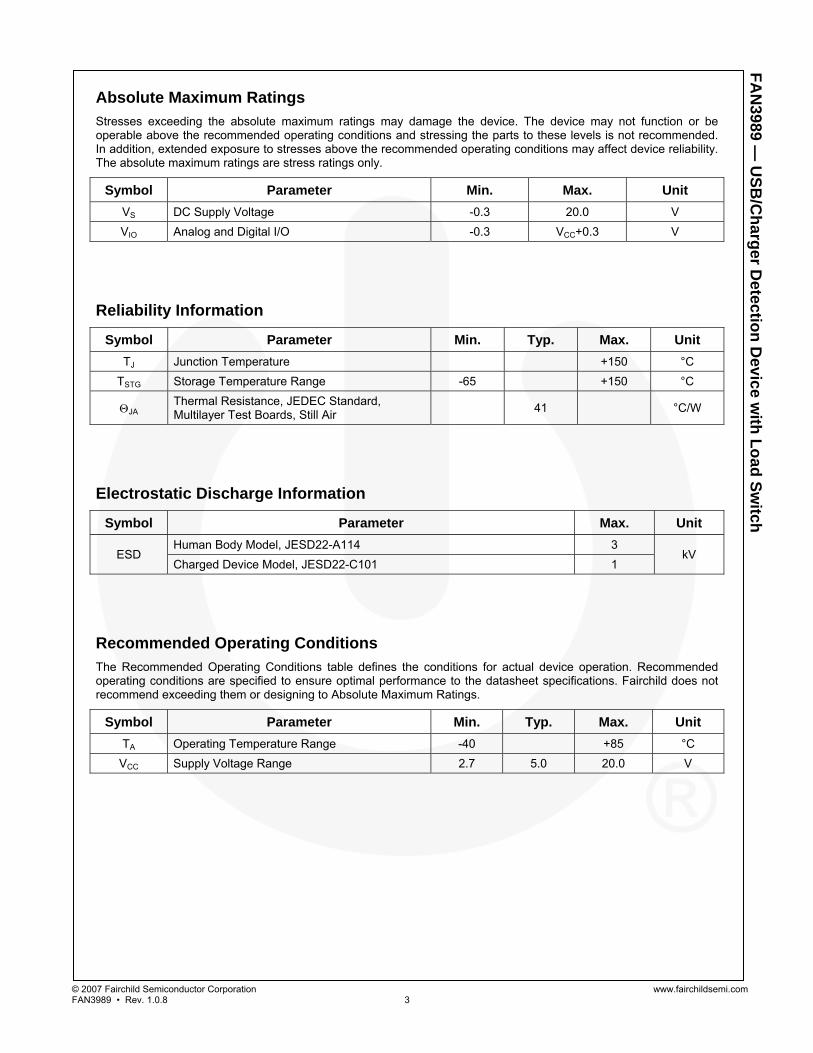
Absolute Maximum Ratings
Stresses exceeding the absolute maximum ratings may damage the device. The device may not function or be operable above the recommended operating conditions and stressing the parts to these levels is not recommended. In addition, extended exposure to stresses above the recommended operating conditions may affect device reliability. The absolute maximum ratings are stress ratings only.
Symbol Parameter Min. Max. Unit
VS DC Supply Voltage -0.3 20.0 V
VIO Analog and Digital I/O -0.3 VCC+0.3 V
Reliability Information
Symbol Parameter Min. Typ. Max. Unit
TJ Junction Temperature +150 °C
TSTG Storage Temperature Range -65 +150 °C
JA Thermal Resistance, JEDEC Standard, Multilayer Test Boards, Still Air
41 °C/W
Electrostatic Discharge Information
Symbol Parameter Max. Unit
ESD Human Body Model, JESD22-A114 3
kV Charged Device Model, JESD22-C101 1
Recommended Operating Conditions
The Recommended Operating Conditions table defines the conditions for actual device operation. Recommended operating conditions are specified to ensure optimal performance to the datasheet specifications. Fairchild does not recommend exceeding them or designing to Absolute Maximum Ratings.
Symbol Parameter Min. Typ. Max. Unit
TA Operating Temperature Range -40 +85 °C
VCC Supply Voltage Range 2.7 5.0 20.0 V

© 2007 Fairchild Semiconductor Corporation www.fairchildsemi.com FAN3989 • Rev. 1.0.8 4
FA
N3989 —
US
B/C
harg
er Detectio
n D
evice with
Lo
ad S
witch
DC Electrical Characteristics
TA = 25°C, VCC = 5.0V, unless otherwise noted.
Symbol Parameter Conditions Min. Typ. Max. Units
Supply
VS Supply Voltage Range VS Range 2.7 5.0 20.0 V
ICC Quiescent Supply Current VS = +5.0V, D+ D- Shorted 1.2 2.0 mA
tSUPPLY Power-Up Stabilization Time VS = +5.0V, D+ D- Shorted 10 ms
Input Characteristics
CD+ Input Capacitance 1.5 2.0 pF
CD- Input Capacitance 1.5 2.0 pF
Ioff D+ Off Leakage Current VBUS = 0V or 5V VIN on D+ = 5V 1 µA
Ioff D- Off Leakage Current VBUS = 0V or 5V VIN on D- = 5V 1 µA
Output Characteristics
OVDETECT Over-Voltage Threshold Detect
VS = +5.0V, Flag2 = LOW 5.8 6.2 6.5 V
OVHYST Over-Voltage Hysteresis Voltage Sweep through Upper and Lower Trip Points
100 mV
UVDETECT Under-Voltage Threshold Detect
VS = +5.0V, Flag2 = LOW 3.0 3.3 3.6 V
UVHYST Under-Voltage Hysteresis Voltage Sweep through Upper and Lower Trip Points
100 mV
VOH FLAG1/ FLAG2
Minimum HIGH Output Voltage
VS = +5.0V, IOH = -20µA 2.4 V
VOL FLAG1/ FLAG2
Maximum LOW Output Voltage
VS = +5.0V, IOL = 20µA 0.3 V
VOL
LS_CTRL Maximum LOW Output Voltage
VS = +5.0V, IOL = 100µA 0.3 V
VBDSS Drain Source Breakdown Voltage
VGS = 0V, ID = -250µA -20 V
RDSON Static Drain-Source On Resistance
VGS = -5.0V, IP = 1A 186 mΩ
Ciss Input Capacitance VDS = -10V, VGS = 0V, f = 1.0MHz
330 pF
Coss Output Capacitance 80 pF
td(on) PMOS Turn-On Delay Time VDD = -5V, IP = -0.5A, VGS = -4.5V, RGEN = 6Ω
5 µs
td(off) PMOS Turn-Off Delay Time 14 µs

© 2007 Fairchild Semiconductor Corporation www.fairchildsemi.com FAN3989 • Rev. 1.0.8 5
FA
N3989 —
US
B/C
harg
er Detectio
n D
evice with
Lo
ad S
witch
Typical Performance Characteristics
VCC = 2.7V-7.0V
0.40
0.50
0.60
0.70
0.80
0.90
1.00
2.7
0
2.9
0
3.1
0
3.3
0
3.5
0
3.7
0
3.9
0
4.1
0
4.3
0
4.5
0
4.7
0
4.9
0
5.1
0
5.3
0
5.5
0
5.7
0
5.9
0
6.1
0
6.3
0
6.5
0
6.7
0
6.9
0
VCC
mA Icc
VCC = 8.0V- 21V
0.4
0.6
0.8
1
1.2
1.4
1.6
1.8
8 9
10
11
12
13
14
15
16
17
18
19
20
21
VCC
mA ICC
Figure 4. ICC vs. VCC (2.7V-7.0V) No Load Figure 5. ICC vs. VCC (8.0V-21V) No Load
RON vs VCC
180.0
182.0
184.0
186.0
188.0
190.0
192.0
3.4
5
3.5
5
3.6
4
3.7
4
3.8
3
3.9
3 4
4.1
2
4.2
2
4.3
1
4.4
1
4.5
4.6
4.7
4.8
4.9
4.9
8
5.0
8
5.1
8
5.2
7
5.3
7
5.4
6
5.5
6
5.6
5
5.7
5
5.8
5
5.9
4
VCC
m RON
Figure 6. RON vs. VCC (10 Load)
Figure 7. Turn-On Time

© 2007 Fairchild Semiconductor Corporation www.fairchildsemi.com FAN3989 • Rev. 1.0.8 6
FA
N3989 —
US
B/C
harg
er Detectio
n D
evice with
Lo
ad S
witch
Typical Performance Characteristics (Continued)
Figure 8. Turn-Off Time
Figure 9. No Fault on Flag 1, Skew=65ns

© 2007 Fairchild Semiconductor Corporation www.fairchildsemi.com FAN3989 • Rev. 1.0.8 7
FA
N3989 —
US
B/C
harg
er Detectio
n D
evice with
Lo
ad S
witch
Typical Performance Characteristics (Continued)
Figure 10. PC Data Running D+/D- (Flag 1 and Flag 2 at Correct Levels)
Figure 11. Standard USB Charger Plug-In

© 2007 Fairchild Semiconductor Corporation www.fairchildsemi.com FAN3989 • Rev. 1.0.8 8
FA
N3989 —
US
B/C
harg
er Detectio
n D
evice with
Lo
ad S
witch
Applications Information
LSctrl
Logi c
VBUS
USBDevice
Std USB /Charge rDetec t
D-
VOUT
Flag 2
Flag 1
Comparato rOVPUVP
1.5K
VDD
R s ens e
Std 15K pull-dow non D- input by US Bdevice and 1.5K pull-u pon D+ by USB transceiver .
USB Transceive r
Battery
D+
15K
Contro l
U SB
GndD +D -
VBUS
Logic
GND
Figure 12. Mobile Phone Battery Charging System with USB Interface
The FAN3989 sets the FLAG1 pin to logic HIGH or LOW as an indicator to the system controller that a standard USB device or a charger is connected to the USB port. The FAN3989 also monitors the VBUS for over- or under-voltage conditions. If VBUS is less than 3.3V or greater than 6.0V, the FLAG2 pin is set LOW and the internal load switch control pin is set HIGH, turning off the PMOS switch.
In a standard USB configuration, there is a switch in the USB transceiver that is always on in full-speed mode. It is on during the transition from full-speed to high-speed mode and turned off after enumeration is
complete. If D+ and D- are shorted when a charger is plugged into the USB port, the USB switch is on and pulled to VDD, which is about 3V, making both D+ and D- HIGH. Flag1 is also set HIGH, indicating that a charging device is connected to the port. If D+ and D- are connected to a standard USB device, the D+ is pulled to VDD and D- is set low (due to the 15KΩ pull-down resistor on the USB device) and flag1 is LOW. If D+ and D- are open (floating), D+ is pulled to VDD and D- floats LOW, which makes flag1 LOW.

© 2007 Fairchild Semiconductor Corporation www.fairchildsemi.com FAN3989 • Rev. 1.0.8 9
FA
N3989 —
US
B/C
harg
er Detectio
n D
evice with
Lo
ad S
witch
Applications Information (Continued)
VOUT
D+
Contro l
R s en s e
U S B
G ndD +D -
V BUS
GND
VBUS
D-
Flag 2Comparato rOVPUV P
Batter y
Logi c
LSctrl
1M
Std USB /Charge rDetec t
5M
Flag 1
Logi c
V DD Figure 13. Mobile Phone Battery Charging System without USB Interface
The FAN3989 sets the FLAG1 pin to logic HIGH or LOW as an indicator to the system controller that a standard USB device or a charger is connected to the USB port. The FAN3989 also monitors the VBUS for over- or under-voltage conditions. If VBUS is less than 3.3V or greater than 6.0V, the FLAG2 pin is set LOW and the internal load switch control pin is set HIGH, turning off the PMOS switch.
Where a USB transceiver is not incorporated or there is a switch between the USB port and the FAN3989, external resistors are used to set the correct input logic states on the D+ and D- inputs. A 5MΩ pull-down on the D- line and a 1MΩ pull-up to VDD on the D+ line are recommended. If a charger is plugged into
the USB port (D+ and D- shorted), the voltage divider of 1M and 5M put a voltage of 2.3V on the D+D- inputs and flag1 is HIGH, indicating a charger is connected to port.
If the USB port is connected to a standard USB device, the D+ input is pulled up to VDD and is in parallel with the 1.5KΩ on a USB transceiver with a parallel R value of 1.497KΩ. The D- input is connected to a 15KΩ pull-down by the USB device and in parallel with 5MΩ with a parallel R value of 14.955KΩ. This condition forces flag1 LOW. If D+ and D- are open (floating), D+ is pulled to VDD and D- floats LOW, which forces flag1 LOW.

© 2007 Fairchild Semiconductor Corporation www.fairchildsemi.com FAN3989 • Rev. 1.0.8 10
FA
N3989 —
US
B/C
harg
er Detectio
n D
evice with
Lo
ad S
witch
PCB Layout Guidelines
Please also see Fairchild Semiconductor applications note AN-5067 — PCB Land Pattern Design and Surface Mount Guidelines for MLP Packages
Pad1 This exposed DAP is connected to the internal FET drain and labeled VOUT on the device. The pad should be connected to VOUT pin of the device or left floating. It
should never be connected to the ground, power plane, or Pad2.
Pad2 This exposed DAP is connected to an internal die substrate that is at a ground potential. The pad should be left floating or can be connected to ground plane. This pad should never be connected to Pad1 or the power plane.
Figure 14. PCD / Pad Layout

© 2007 Fairchild Semiconductor Corporation www.fairchildsemi.com FAN3989 • Rev. 1.0.8 11
FA
N3989 —
US
B/C
harg
er Detectio
n D
evice with
Lo
ad S
witch
Physical Dimensions
Figure 15. 8-Lead Molded Leadless Package (MLP) Package drawings are provided as a service to customers considering Fairchild components. Drawings may change in any manner without notice. Please note the revision and/or date on the drawing and contact a Fairchild Semiconductor representative to verify or obtain the most recent revision. Package specifications do not expand the terms of Fairchild’s worldwide terms and conditions, specifically the warranty therein, which covers Fairchild products. Always visit Fairchild Semiconductor’s online packaging area for the most recent package drawings: http://www.fairchildsemi.com/packaging/.

© 2007 Fairchild Semiconductor Corporation www.fairchildsemi.com FAN3989 • Rev. 1.0.8 12
FA
N3989 —
US
B/C
harg
er Detectio
n D
evice with
Lo
ad S
witch