Embed Size (px)
Citation preview

Faculty of Computer Science
CMPUT 229 © 2006
Digital Logic
From Switches to Memories
© 2006
Department of Computing Science
CMPUT 229
Reading Material
These slides are based on the Text by Patt and
Patel: Introduction to Computing Systems: From
Bits & Gates to C & Beyond.
The concepts covered here are presented in
Chapter 2 of Alan Clements’ textbook.
© 2006
Department of Computing Science
CMPUT 229
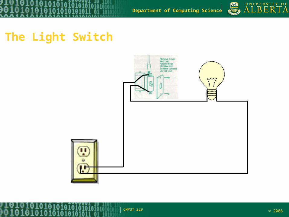
The Light Switch
© 2006
Department of Computing Science
CMPUT 229
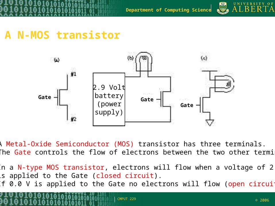
A N-MOS transistor
A Metal-Oxide Semiconductor (MOS) transistor has three terminals. The Gate controls the flow of electrons between the two other terminals.
In a N-type MOS transistor, electrons will flow when a voltage of 2.9 Vis applied to the Gate (closed circuit).If 0.0 V is applied to the Gate no electrons will flow (open circuit).
2.9 Voltbattery(powersupply)
Gate GateGate
© 2006
Department of Computing Science
CMPUT 229
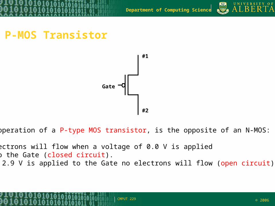
P-MOS Transistor
The operation of a P-type MOS transistor, is the opposite of an N-MOS:
- electrons will flow when a voltage of 0.0 V is applied to the Gate (closed circuit).- If 2.9 V is applied to the Gate no electrons will flow (open circuit).
Gate
#1
#2
© 2006
Department of Computing Science
CMPUT 229
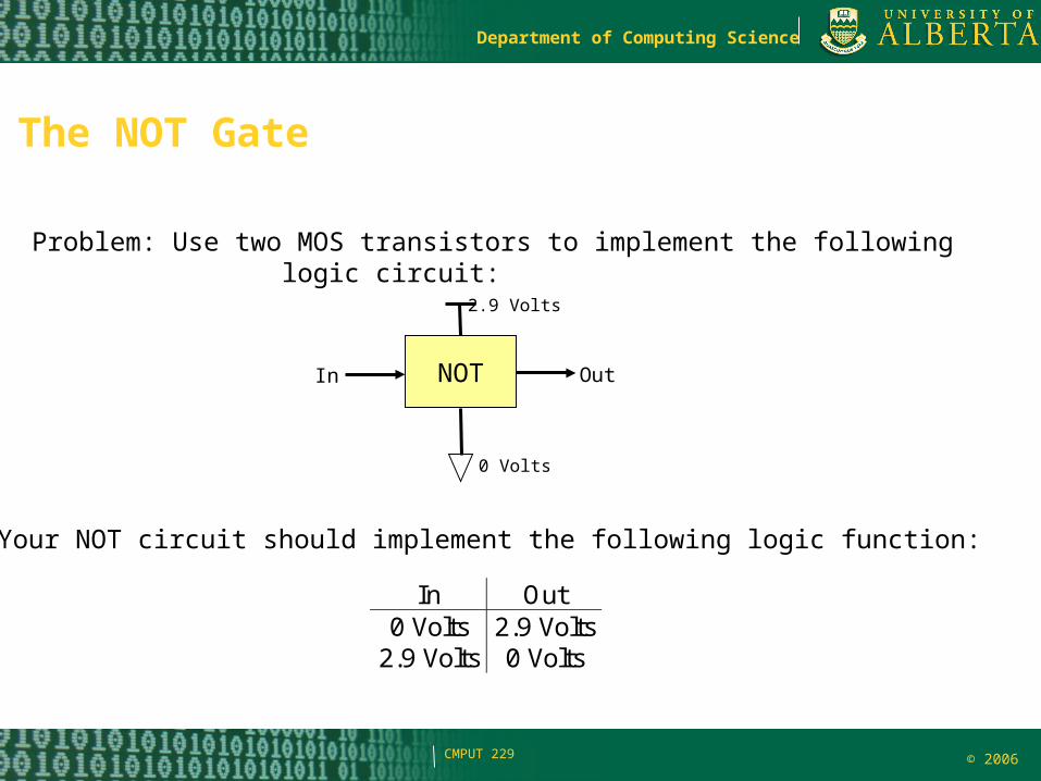
The NOT Gate
Problem: Use two MOS transistors to implement the following logic circuit:
NOT
2.9 Volts
0 Volts
In Out
Your NOT circuit should implement the following logic function:
In Out 0 Volts 2.9 Volts
2.9 Volts 0 Volts
© 2006
Department of Computing Science
CMPUT 229
2.9V0V
0 Volts
2.9 Volts
0V
2.9 Volts
0 Volts
2.9V
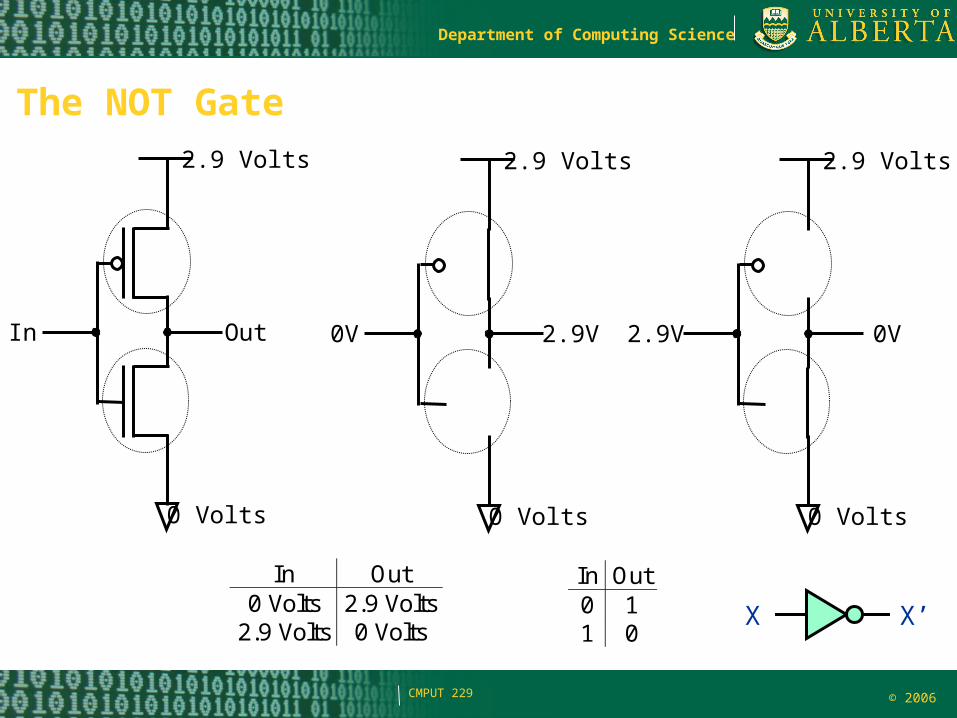
The NOT Gate
In
2.9 Volts
0 Volts
Out
In Out 0 Volts 2.9 Volts
2.9 Volts 0 Volts
In Out 0 1 1 0
X X’
© 2006
Department of Computing Science
CMPUT 229
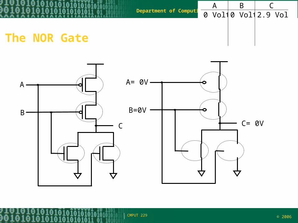
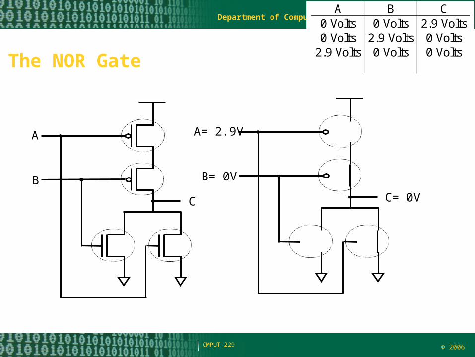
The NOR Gate
A B C 0 Volts 0 Volts 2.9 Volts
A
C
B
A= 0V
C= 0V
B=0V
© 2006
Department of Computing Science
CMPUT 229
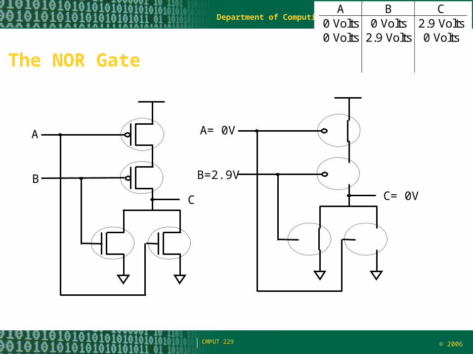
The NOR Gate
A B C 0 Volts 0 Volts 2.9 Volts 0 Volts 2.9 Volts 0 Volts
A
C
B
A= 0V
C= 0V
B=2.9V
© 2006
Department of Computing Science
CMPUT 229
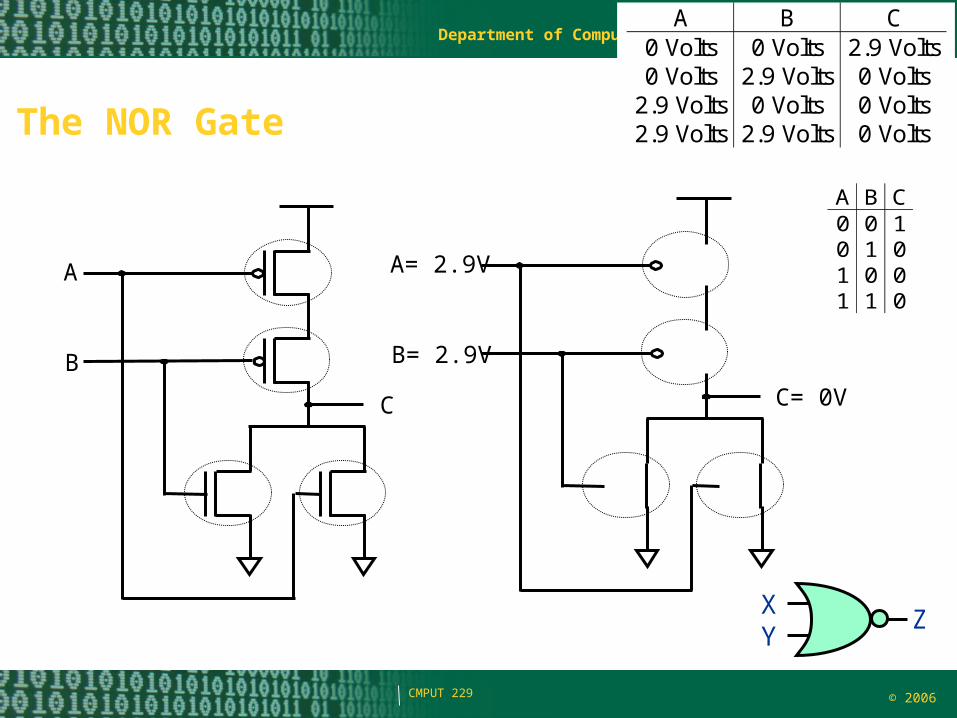
The NOR Gate
A
C
B
A= 2.9V
C= 0V
B= 0V
A B C 0 Volts 0 Volts 2.9 Volts 0 Volts
2.9 Volts 2.9 Volts 0 Volts
0 Volts 0 Volts
© 2006
Department of Computing Science
CMPUT 229
The NOR Gate
A B C 0 Volts 0 Volts 2.9 Volts 0 Volts
2.9 Volts 2.9 Volts
2.9 Volts 0 Volts
2.9 Volts
0 Volts 0 Volts 0 Volts
A
C
B
A= 2.9V
C= 0V
B= 2.9V
A B C 0 0 1 0 1 1
1 0 1
0 0 0
XY
Z
© 2006
Department of Computing Science
CMPUT 229
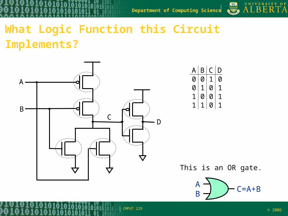
What Logic Function this Circuit Implements?
A
BC
D
A B C D 0 0 1 0 0 1 1
1 0 1
0 0 0
1 1 1
1
This is an OR gate.
AB
C=A+B
© 2006
Department of Computing Science
CMPUT 229
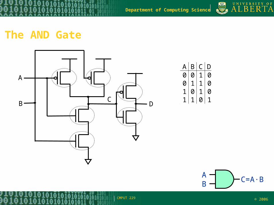
The AND Gate
A
BC
D
A B C D 0 0 1 0 0 1 1
1 0 1
1 1 0
0 0 1
1
AB
C=A·B
© 2006
Department of Computing Science
CMPUT 229
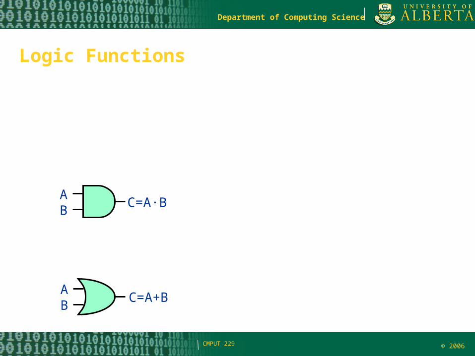
Logic Functions
AB
C=A+B
AB
C=A·B
© 2006
Department of Computing Science
CMPUT 229
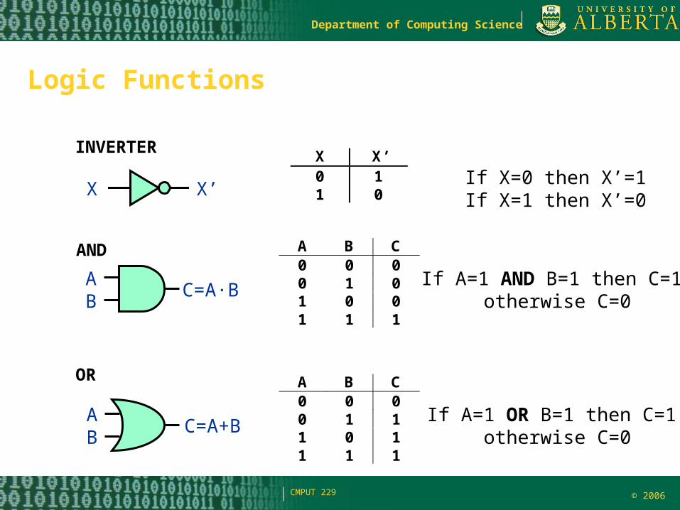
Logic Functions
INVERTER
X X’
X X’0 11 0
If X=0 then X’=1If X=1 then X’=0
OR
AB
C=A+B
A B C0 0 00 1 11 0 11 1 1
If A=1 OR B=1 then C=1 otherwise C=0
AB
C=A·B
A B C0 0 00 1 01 0 01 1 1
If A=1 AND B=1 then C=1 otherwise C=0
AND
© 2006
Department of Computing Science
CMPUT 229
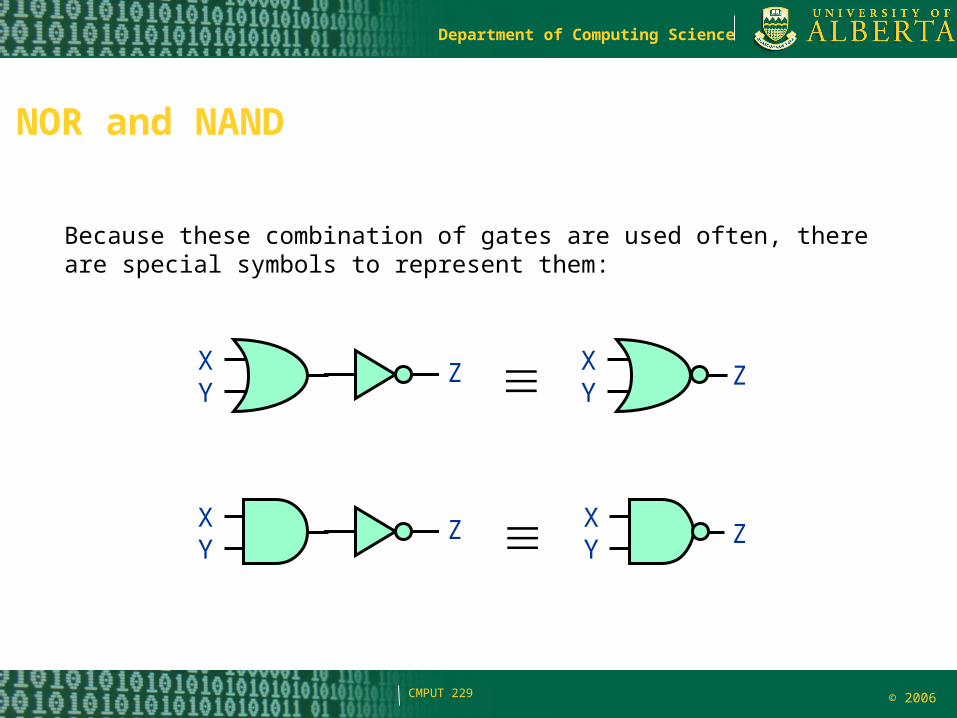
NOR and NAND
Because these combination of gates are used often, thereare special symbols to represent them:
XY
Z XY
Z
ZXY
XY
Z
© 2006
Department of Computing Science
CMPUT 229
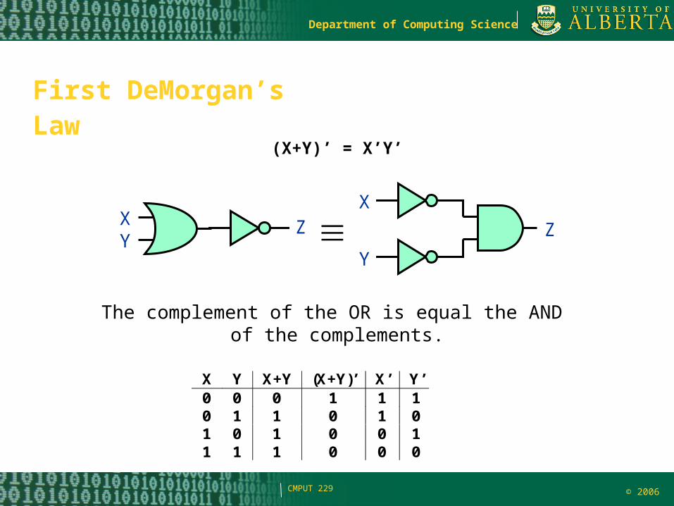
First DeMorgan’s Law
The complement of the OR is equal the AND of the complements.
(X+Y)’ = X’Y’
XY
Z
X Y X+Y (X+Y)’ X’ Y’ X’Y’0 0 0 1 1 1 10 1 1 0 1 0 01 0 1 0 0 1 01 1 1 0 0 0 0
Z
Y
X
© 2006
Department of Computing Science
CMPUT 229
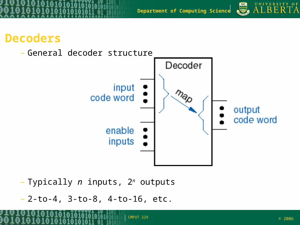
Decoders– General decoder structure
– Typically n inputs, 2n outputs
– 2-to-4, 3-to-8, 4-to-16, etc.
© 2006
Department of Computing Science
CMPUT 229
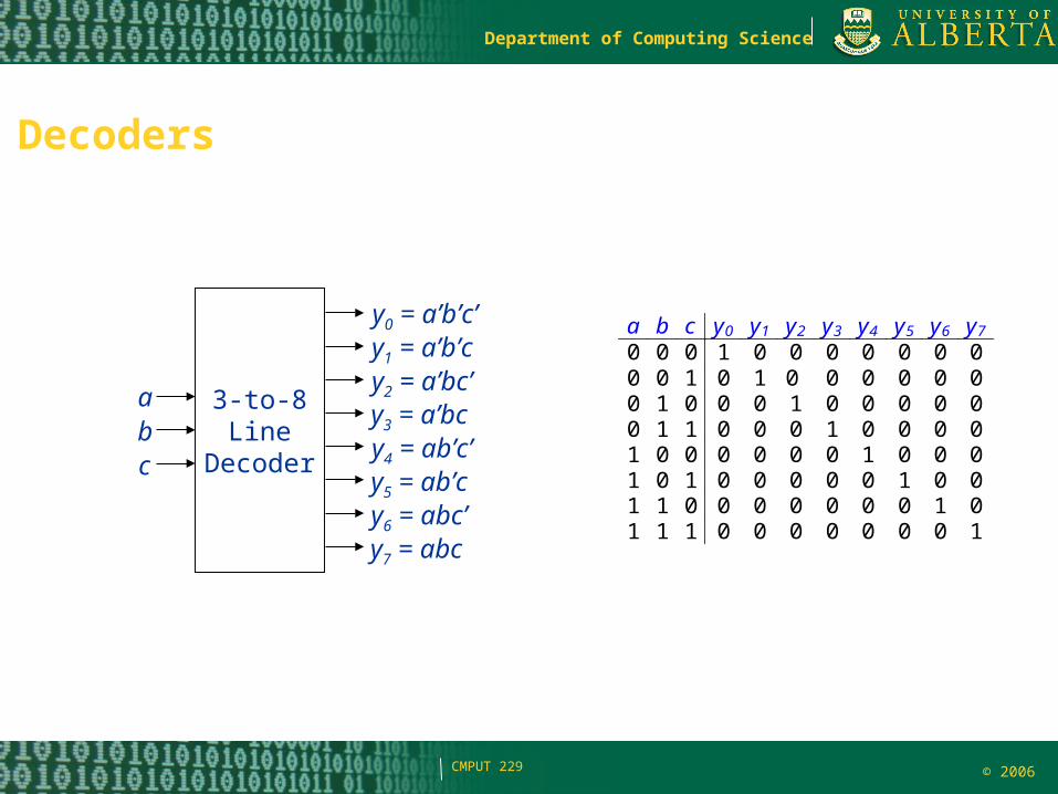
Decoders
3-to-8Line
Decoder
y0 = a’b’c’y1 = a’b’cy2 = a’bc’y3 = a’bcy4 = ab’c’y5 = ab’cy6 = abc’y7 = abc
abc
a b c y0 y1 y2 y3 y4 y5 y6 y7 0 0 0 1 0 0 0 0 0 0 0 0 0 1 0 1 0 0 0 0 0 0 0 1 0 0 0 1 0 0 0 0 0 0 1 1 0 0 0 1 0 0 0 0 1 0 0 0 0 0 0 1 0 0 0 1 0 1 0 0 0 0 0 1 0 0 1 1 0 0 0 0 0 0 0 1 0 1 1 1 0 0 0 0 0 0 0 1
+
© 2006
Department of Computing Science
CMPUT 229
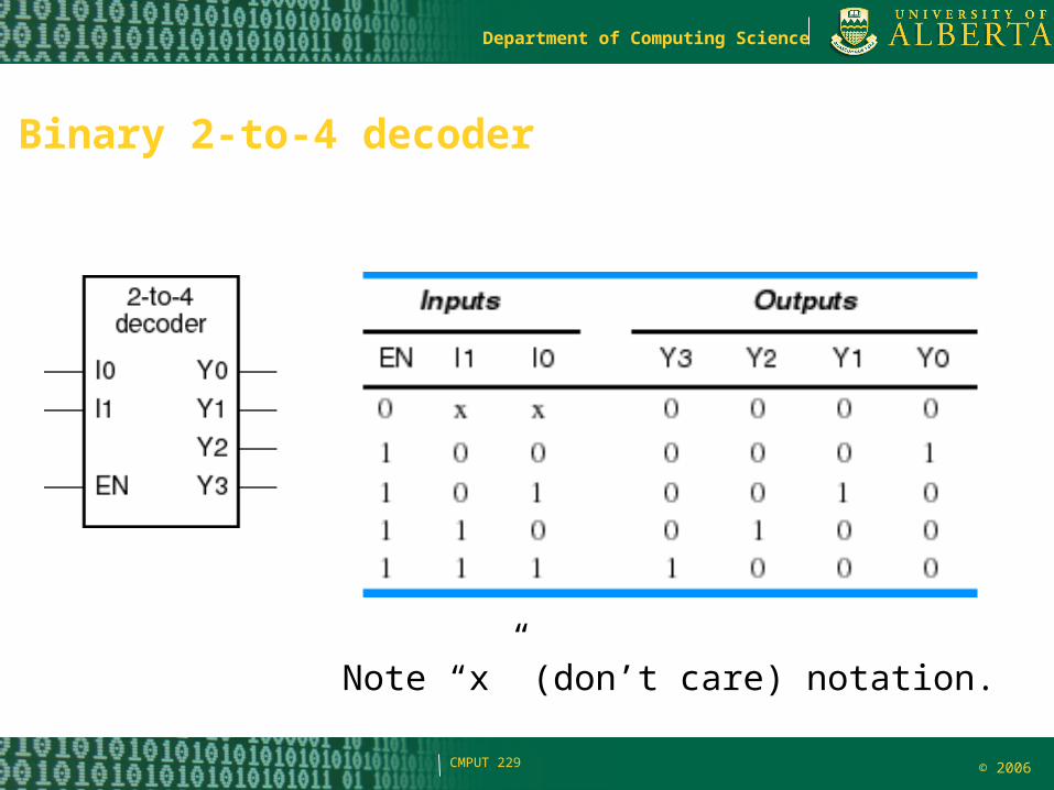
Binary 2-to-4 decoder
Note “x” (don’t care) notation.
© 2006
Department of Computing Science
CMPUT 229
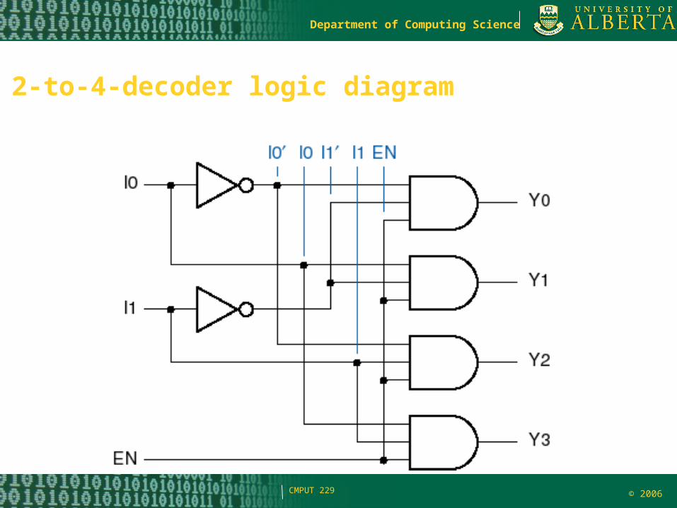
2-to-4-decoder logic diagram
© 2006
Department of Computing Science
CMPUT 229
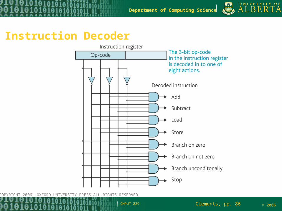
Instruction Decoder
Clements, pp. 86
COPYRIGHT 2006 OXFORD UNIVERSITY PRESS ALL RIGHTS RESERVED
© 2006
Department of Computing Science
CMPUT 229
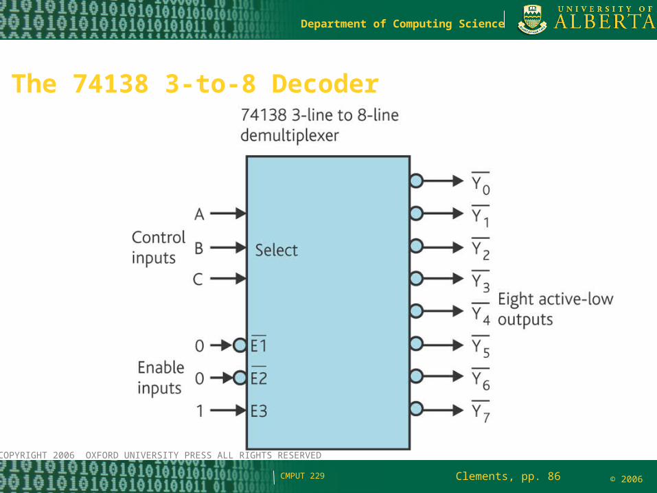
The 74138 3-to-8 Decoder
Clements, pp. 86
COPYRIGHT 2006 OXFORD UNIVERSITY PRESS ALL RIGHTS RESERVED
© 2006
Department of Computing Science
CMPUT 229
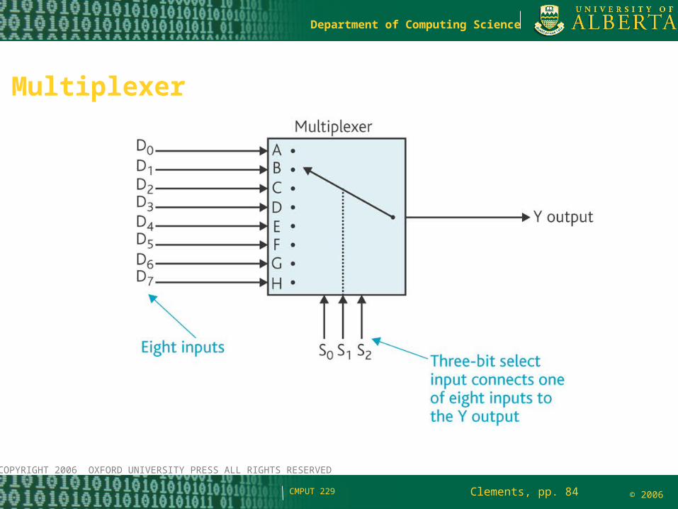
Multiplexer
Clements, pp. 84
COPYRIGHT 2006 OXFORD UNIVERSITY PRESS ALL RIGHTS RESERVED
© 2006
Department of Computing Science
CMPUT 229
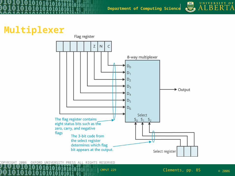
Multiplexer
Clements, pp. 85
COPYRIGHT 2006 OXFORD UNIVERSITY PRESS ALL RIGHTS RESERVED
© 2006
Department of Computing Science
CMPUT 229
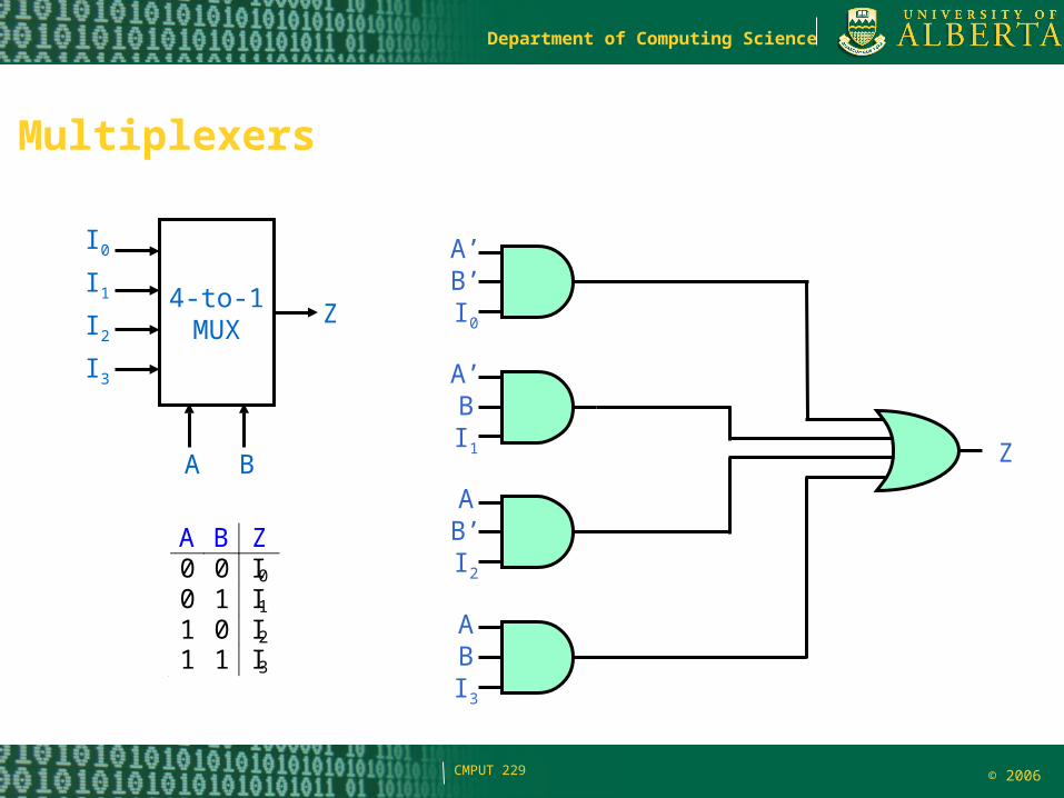
Multiplexers
4-to-1MUX
I0
I1
I2
I3
A B
Z
A B Z 0 0 I0 0 1 I1 1 0 I2 1 1 I3
+
ABI3
AB’I2
A’BI1
A’B’I0
Z
© 2006
Department of Computing Science
CMPUT 229
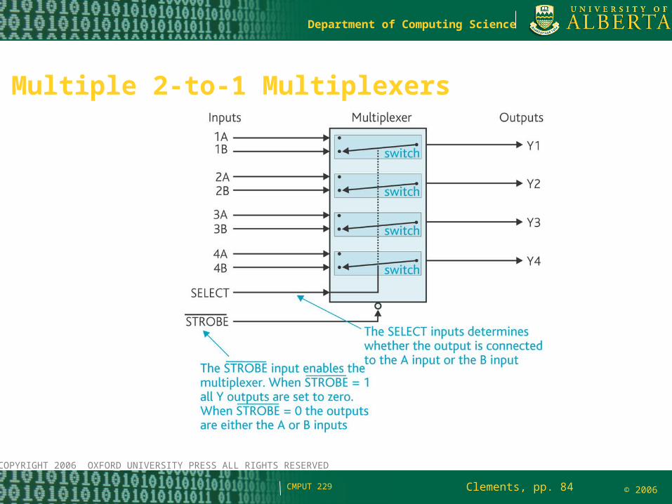
Multiple 2-to-1 Multiplexers
Clements, pp. 84
COPYRIGHT 2006 OXFORD UNIVERSITY PRESS ALL RIGHTS RESERVED