Embed Size (px)
Citation preview

Thin film solar cells based on chalcogenides
Bindu Krishnan
Facultad de Ingeniería Mecánica y Eléctrica,
Universidad Autónoma de Nuevo León,
San Nicolás de los Garza, Nuevo León, México. C.P- 66450.

Objectives
Projects
Results
Facilities
Research group
Publications

Thin film materials
CuInSe2 and alloys, SnS, Sb2S3, AgSbSe2 and
alloys, CZTS, CuSbS2 and CdS, TCOs
Low cost and simple methods
Chemical Bath Deposition (CBD)
Spray Pyrolysis
Thermal Evaporation
Laser annealing and device fabrication, plasma treatments

Dr. Bindu Krishnan
Polycrystalline silver antimony selenide for thin films for solar cells - Ciencia Basica
Copper indium selenide thin films by a non-toxic method for solar cell applications – Apoyo licenciatura - Bindu Krishnan
Preparation of semiconducting thin films for solar cell applications by laser irradiation and their characterization using photothermal and photoacoustic techniques –CIAM
Dr. Sadasivan Shaji
Preparation and characterization of nanoparticles by laser ablation in liquid media
Dr. David Avellaneda
SnS based solar cells - Retention

Estructura fotovoltaica p-AgSbSe2/n-CdS: Estudio del efecto de la relación Ag/Sb y sus tratamientos de postdeposicion –Dra. Bindu Krishnan
Preparation and characterization of ZnO thin films by electron beam evapoartion – Dr.Sadasivan shaji
Preparation and characterization of Sn doped ZnO thin films by spray pyrolisis – Dra. Ana Maria Arato
PROMEP – SEP Laser assisted material processing- Dr. Sadasivan
Shaji
Preparation and characterization of ZnO:Al thin films by spray pyrolisis – Dra. Ana Maria Arato


-0.4 -0.2 0.0 0.2 0.4 0.6 0.8 1.0
-0.20
-0.15
-0.10
-0.05
0.00
0.05
0.10Sb
2S
3-5h, C 5s
Voc
= 556 mV
Isc
=0.08 mA/cm2
I (m
A/c
m2)
V (Volt)
dark
light
CdS – 50 nm
Glass
Sb2S3:C (500 nm)
ITO
- +
light
Emma Cardenas, A. Arato, E. Perez-Tijerina, T.K. Das Roy, G. Alan Castillo, B. Krishnan, Carbon-doped Sb2S3
thin films: Structural, optical and electrical properties, Solar Energy materials and Solar Cells, 93, 33– 36
(2009)
Sb2S3 as PV material

AgSbSe2 and AgSb(S,Se)2 as PV material
Glass/Sb2S3/Ag2Se/Se/Ag
350 C in vacuum for 1 hGlass/Sb2S3/Ag2Se/Ag350 C in vacuum for 1 h

CdS – 50 nm
Glass
p-AgSbSe2 (500 nm)
ITO
- +
light
AgSbSe2 and AgSb(S,Se)2 as PV material

Laser annealing - modification of properties
10 20 30 40 50 60 70
0
100
0
100
2 (degree)
a) Sb2S
3/Glass
unexposed
(240)
(30
1)(2
21
)
(211)(23
0)
(130)
b) Sb2S
3/Glass
Inte
nsity (
a.u
)
80 W/cm2, 2 min
(312)
(501)(141)
(120)
(020)
Photograph of Sb2S3
asprepared and irradiated
Sample
DPSS
LASER
S. Shaji et al Journal of Physics D: Applied Physics, 43 (2010) 075404.
XRD patterns of Sb2S3 before
and after laser irradiation
-0.4 -0.2 0.0 0.2 0.4 0.6 0.8 1.0
-1.0x10⁻³
0.0
1.0x10⁻³
(b) illumination
(a) dark
J (
A/c
m2)
V (Volt) CdS – 50 nm
Glass
Sb2S3:C (500 nm)
ITO
- +
light
A. Arato, et al Thin solid films 517 (2009) 2493-2496
Laser annealing – device formation

CuInSe2 thin films by a non-toxic process:
Glass/In/Se/Cu2Se heated
350 – 400 C in vacuum for 1 h
SeCu2Se
Glass
Glass
CuInSe2
In
350 – 400 C in
vacuum for 1 h
PVDCBD
Accepted for presentation in MRS
spring meeting, 2011

0
50
1000
50
100
20 30 40 50 60 70 800
100
2 (degree)
(1
02)
(112)
(103)
(110)
(101)
(002)
(100)
ZnO -hexagonal
PDF#36-1451
ZnO
Inte
nis
ty (
a.u
)
ZnO:Sb
(004)
(103)
(102)
(100)
(002)
(101)
(110)
(004)
(200)
(112)
(103)
(110)
(102)
(101)
(002)
(100)
EMRS-2008 , Strasbourg, France
ZnO and ZnO:Sb
10 20 30 40 50 60 70
(112)(103)
(110)(102)
(101)
(002)
(100)
---- PDF 36-1451
ZnO 0.1M
Inte
ns
ida
d (
u.a
.)
2
0% Sn
1% Sn
3% Sn
5% Sn
Saida Garcia, Tesis de Maestria, FIME-UANL, 2011
ZnO and ZnO:Sn
ZnO – by spray pyrolysis
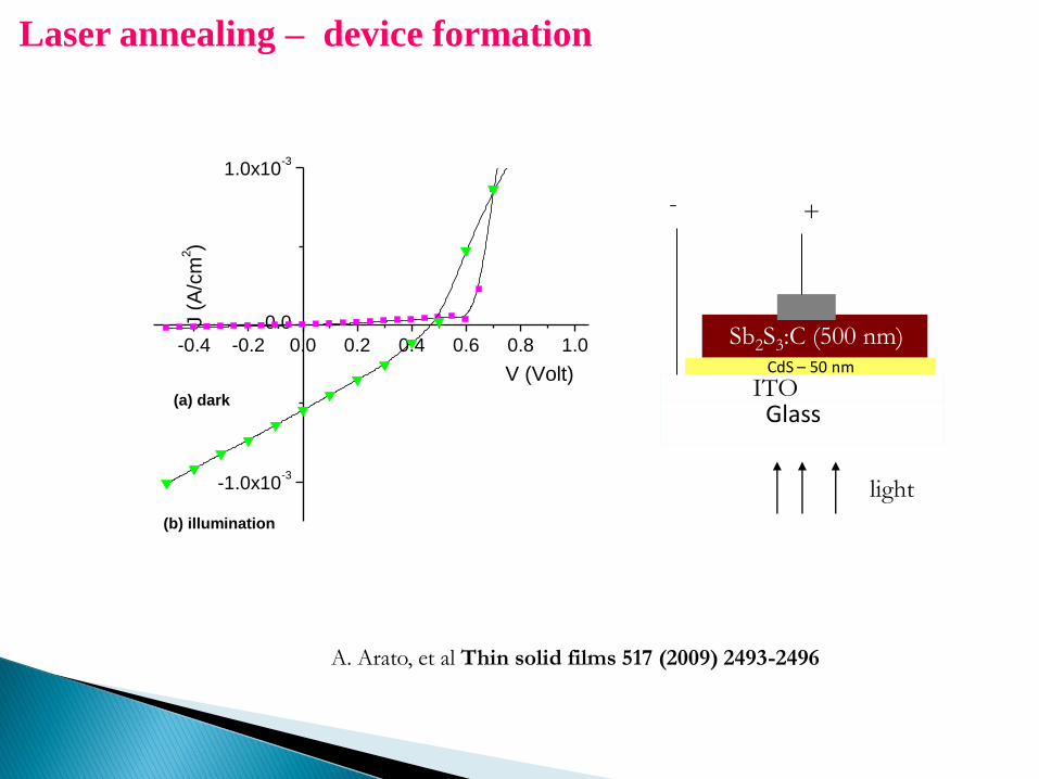
Two source thermal evaporation
unit
Vacuum
furnace – 400
C
Constant temperature bath
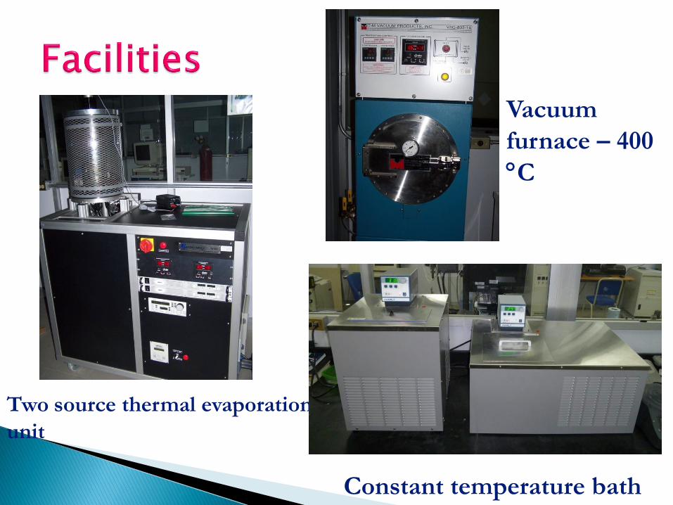
150 W Solar simulator
Hall Effect measurement system
I-V Characterization unit

DPSS Laser , 8000 m W, 532 nm, CW
DPSS DMP VA532/8
Wavelength (nm) 532
DPSS Laser , 4000 mW,
457 nm, CW


Dr. Bindu Krishnan
Dr. Sadasivan Shaji
Dr. David Avellaneda
Dr. Tushar Kanti Das Roy
Dr. Alan Castillo
Dr. Preethy Rajesh
Dr. Rajesh Nair
Dr. Ana Maria AratoDocotoral, Master’s and Undergraduate students

Modification of optical and electrical properties of chemical bath deposited CdS using Plasma Treatments, G. Gonzalez, B. Krishnan, G.A. Castillo, T.K. Das Roy and S. Shaji, Thin Solid Films 2011. (article in press) doi:10.1016/j.tsf.2011.01.374 .
p-Type CuSbS2 thin films by thermal diffusion of copper into Sb2S3, C. Garza, S.Shaji, A.Arato, E.Perez Tijerina, G.Alan Castillo, T.K.Das Roy, B.Krishnan, Solar Energy Materials & Solar Cells (article in press) (2010), doi:10.1016/j.solmat.2010.06.011.
Chemically deposited Sb2S3 thin films for optical recording, S. Shaji, A. Arato, J. J. O’Brien, J. Liu , G. Alan Castillo, M I Mendivil Palma, T.K. Das Roy and B. Krishnan, Journal of Physics D: Applied Physics, 43 (2010) 075404.
A. Arato, E. Cárdenas, S. Shaji, J. J. O’Brien, J. Liu , G. Alan Castillo, T.K. Das Roy and B. Krishnan, Sb2S3:C/CdS p-n junction by laser irradiation, Thin solid films 517 (2009) 2493-2496
Emma Cardenas, A. Arato, E. Perez-Tijerina, T.K. Das Roy, G. Alan Castillo, B. Krishnan, Carbon-doped Sb2S3 thin films: Structural, optical and electrical properties, Solar Energy materials and Solar Cells, 93, 33– 36 (2009)
Chemically deposited silver antimony selenide thin films for photovoltaic applications, Jorge Oswaldo, S. Shaji, A. Arato, T.K Das Roy, G.A. Castillo and B. Krishnan, , Mater. Res. Soc. Symp. Proc. Vol. 1165 © 2009 Materials Research Society, 1165-M08-25.
K. Bindu, Ana Maria Arato, E. Cardenaz, T.K Das Roy and G. Alan Castillo, On the structure, morphology, and optical properties of chemical bath deposited Sb2S3 thin films, Applied Surface Science 254 (2008) 3200.

SEP-CONACYT
PAICYT-UANL
PROMEP