Embed Size (px)
Citation preview
1755
Pure Appl. Chem., Vol. 79, No. 10, pp. 1755–1769, 2007.doi:10.1351/pac200779101755© 2007 IUPAC
Factors affecting wettability and bond strengthof solder joint couples*
Natalia Sobczak1,‡, Artur Kudyba1, Rafal Nowak1,Waldemar Radziwill1, and Krystyna Pietrzak2
1Foundry Research Institute, 73 Zakopianska Street, 30-418 Cracow, Poland;2Motor Transport Institute, 88 Jagiellonska Street, 03-391 Warsaw, Poland
Abstract: The paper discusses the scientific understanding of the role of interfacial phenom-ena in joining of dissimilar materials using liquid-phase-assisted processes. From the exam-ple of the Sn-alloy/Cu system, it is demonstrated that interaction in the liquid solder/substratecouples is accompanied by a number of complex interfacial reactions leading to significantchanges in the structure and chemistry of interfaces (solder/substrate, solder/environment,substrate/environment) and remaining solder layer that finally influence the mechanical prop-erties of solder joints.
The experimental data on wetting behavior, interface characterization, and mechanicalproperties of different solder/metal substrate couples are analyzed in order to display the roleof such factors as time and temperature of interaction, environment (protective atmosphere,flux), presence of oxide films on interfaces, alloying additions to a solder, formation of inter-facial phases, and porosity.
Keywords: soldering; wettability; sessile drop test; interfaces; bond strength.
INTRODUCTION
The wetting of solid metal substrates by metal melts, accompanied by the formation of interfaces andresulting in the creation of bonding between dissimilar materials, belong to high-temperature phenom-ena of fundamental importance for improving industrial liquid-phase-assisted joining processes such assoldering.
The degree of wetting is usually estimated by the value of contact angle θ. Considering a dropresting at mechanical and thermodynamical equilibrium on a perfectly flat surface of nondeformablesolid substrate, Young determined θ from the mechanical equilibrium of the drop by equation of thehorizontal force balance at the three-phase line among the liquid (σlv), the solid (σsv) and solid/liquid(σsl) interfacial tensions [1]
σsv – σsl = σlvcosθ (1)
The contact angle presents a key technological parameter in selecting materials and correspon-ding joining processes because a good wetting (θ << 90°) is required in order to produce high-qualitysolder joints, whereas solderability is optimized when θ is minimized. At the same time, following theYoung–Dupré equation
Wa = σlv(1 + cosθ) (2)
*Paper based on a presentation at the 12th International IUPAC Conference on High Temperature Materials Chemistry(HTMC-XII), 18–22 September 2006, Vienna, Austria. Other presentations are published in this issue, pp. 1635–1778.‡Corresponding author: Tel.: +48 12 261 8526; Fax: +48 12 66 0870; E-mail: [email protected]
the contact angle θ may be considered as a “strength-related” factor since together with σlv it directlyinfluences the work of adhesion Wa, a quantity that characterizes the thermodynamic stability of inter-faces between dissimilar materials and is widely used in practice for prediction of their potential bond-ing properties (low θ tends to correlate with greater Wa).
Literature data on contact angle values for most systems measured by the same sessile dropmethod and at the same temperature show a large scattering caused generally by differences in the sub-strate surface roughness and by pollution from the atmosphere, mainly oxygen, the presence of whichis unavoidable in the gaseous environments of technical high-temperature processes [2–4]. It is well es-tablished that oxygen affects surface tension of such metals as Sn, Pb, and In; those alloys are com-monly used as solders (e.g., at the melting point, oxygen-free Sn has σlv = 598 mNn/m, contrary to535 mN/m for oxygen-rich Sn) [5]. Additionally, oxygen can form oxide films on metallic droplets andon metallic solid substrates, contributing to a dramatic decrease in the apparent σlv value (σlv =470 mNn/m for an oxidized surface [6]) and increase in the apparent contact angle values by tens of de-grees [3,7].
Most of the solder/substrate couples present highly reactive systems in which wetting phenomenaare accompanied by the dissolution of the substrate in molten solder and by complex interfacial reac-tions leading to the formation of intermetallic compound (IMC) layers. It results in significant changesin the structure and chemistry of interfaces and solder itself, thus finally affecting both the solder wet-ting behavior and mechanical properties of solder joints.
This study reviews the current state of knowledge on the role of interfacial phenomena in joiningof dissimilar materials using liquid-phase-assisted joining process such as soldering of electronic ma-terials. New experimental results on the effect of processing parameters on the relationship betweenwetting, interface structure, and mechanical strength of Sn-based solder/Cu couples are discussed inorder to demonstrate such effects as the presence of oxide films on a solder and Cu substrate surfaces,time and temperature of interaction, environment, alloying additions to a solder, and the formation ofinterfacial phases and porosity.
EXPERIMENTAL PROCEDURE
Sessile drop test
The materials were Cu substrates and several Sn-based solders containing different additions of Cu, Ag,In, Bi, Zn, and Pb (given in wt %). Directly before wettability tests, the Cu substrates were polished upto an average roughness of a few nm while the Sn alloy samples were cleaned mechanically, and nextboth Cu substrate and Sn-alloy samples were cleaned ultrasonically in acetone.
The contact angles θ were measured by the sessile drop method described in [2]. The wettabilitytests were carried out in different environments (dynamic vacuum, air, colophony-based flux) under var-ious testing conditions. Two improved procedures were employed for heating the solder/substrate cou-ples:
1. Fast contact heating (CH) with a rate of ∼20 °C min–1 was achieved by introducing the solder/Cucouple into the furnace preheated to the experimental temperature Texp while the time ofdrop/substrate contact was measured from the moment of visually estimated melting of a solderas described in [8]; this procedure is more suitable for investigation of reactive systems since itallows one to reduce the time of contact during heating a couple to Texp, contrary to the widelyused procedure of slow CH when a couple of materials being in contact are first placed in the fur-nace and then long-time heated from room temperature to the test temperature with a rate of ∼1 °Cmin–1 (Fig. 1a);
2. Capillary purification (CP) [4], in which the substrate and the metal were heated separately undervacuum, the metal in a graphite syringe. At the test temperature, a droplet of the metal is me-chanically squeezed out of the graphite syringe and brought in contact with the preheated sub-
N. SOBCZAK et al.
© 2007 IUPAC, Pure and Applied Chemistry 79, 1755–1769
1756
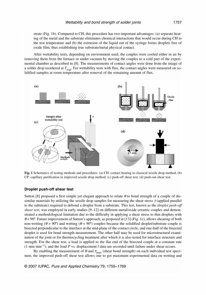
strate (Fig. 1b). Compared to CH, this procedure has two important advantages: (a) separate heat-ing of the metal and the substrate eliminates chemical interactions that would occur during CH tothe test temperature and (b) the extrusion of the liquid out of the syringe forms droplets free ofoxide film, thus establishing true substrate/metal physical contact.
After wettability tests, depending on environment used, the couples were cooled either in air byremoving them from the furnace or under vacuum by moving the couples to a cold part of the experi-mental chamber as described in [8]. The measurements of contact angles were done from the image ofa solder drop reordered at Texp. For wettability tests with flux, the contact angles were measured on so-lidified samples at room temperature after removal of the remaining amount of flux.
Droplet push-off shear test
Sutton [8] proposed a first simple yet elegant approach to relate θ to bond strength of a couple of dis-similar materials by utilizing the sessile drop samples for measuring the shear stress τ (applied parallelto the substrate) required to debond a droplet from a substrate. This test, known as the droplet push-offshear test, was employed in early studies [9–12] on different metal/oxide ceramic couples and demon-strated a methodological limitation due to the difficulty in applying a shear stress to thin droplets withθ < 90º. Future improvement of Sutton’s approach, as proposed in [13] (Fig. 1c), allows shearing of bothnon-wetting (θ > 90º) and wetting (θ < 90º) couples because the solidified droplet/substrate couple isbisected perpendicular to the interface at the mid-plane of the contact circle, and one-half of the bisecteddroplet is used for bond strength measurement. The other half may be used for microstructural exami-nation of the joint or for thermocycling treatment after which it is also tested for interface structure andstrength. For the shear test, a load is applied to the flat end of the bisected couple at a constant rate(1 mm min–1), and the load P vs. displacement l data are recorded until failure under shear occurs.
By enabling the measurement of θ and τmax (shear bond strength) on each individual test speci-men, the improved push-off shear test allows one to get maximum experimental data on wetting and
© 2007 IUPAC, Pure and Applied Chemistry 79, 1755–1769
Wettability and bond strength of solder joints 1757
Fig. 1 Schematics of testing methods and procedures: (a) CH: contact heating in classical sessile drop method; (b)CP: capillary purification in improved sessile drop method; (c) push-off shear test; (d) push-out shear test.
bonding properties, structure and chemistry of the interface in the same test coupon. The authors ap-plied this test to a wide group of metal/ceramic systems [13–18] and demonstrated its convenience andusefulness in investigation of interfacial phenomena with pure Al, Cu, and Ni and Al-alloys.
Taking into account the practical importance of information about shear properties of solder joints(the strain in electronic interconnects is mostly shear due to coefficient of thermal expansion (CTE)mismatch between the solder and the substrate) as well as the fact that in the wettability tests the spec-imens are produced under repeatable and well-controlled conditions, the sessile drop couples might beused as model solder/substrate joints, for which mechanical properties can be easily estimated by theproposed improved push-off shear test. The first attempt of its application reported in [8] also confirmedthe usefulness of the push-off shear test for investigation of the solder/Cu couples.
Push-out shear test
A limited number of measurements were done using a push-out shear test, which is similar to thatwidely used for characterization of the fiber/matrix interfacial strength in fiber-reinforced compositematerials [19]. The solder/Cu couples were produced from Cu rings, whose internal diameter (d =5 mm) was comparable to the diameter of the solder droplets in the sessile drop tests. The hole in theCu rings was filled with molten solder according to the procedure used in wettability tests with flux(230 °C, 5 min; after machining, the Cu rings were ultrasonically cleaned in acetone directly beforetheir contact with a molten solder). The solder/Cu couples were sheared at the same constant rate as inthe push-off shear tests by loading a punch of different diameters φ = 4.92–5 mm (Fig. 1d).
RESULTS
Effect of oxide films
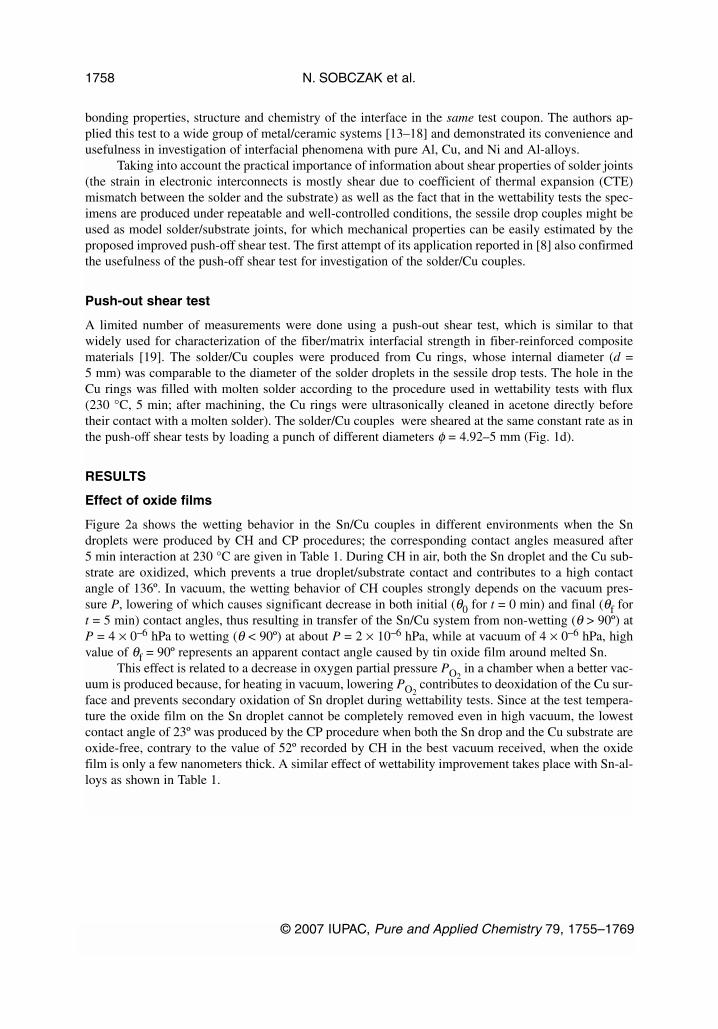
Figure 2a shows the wetting behavior in the Sn/Cu couples in different environments when the Sndroplets were produced by CH and CP procedures; the corresponding contact angles measured after5 min interaction at 230 °C are given in Table 1. During CH in air, both the Sn droplet and the Cu sub-strate are oxidized, which prevents a true droplet/substrate contact and contributes to a high contactangle of 136º. In vacuum, the wetting behavior of CH couples strongly depends on the vacuum pres-sure P, lowering of which causes significant decrease in both initial (θ0 for t = 0 min) and final (θf fort = 5 min) contact angles, thus resulting in transfer of the Sn/Cu system from non-wetting (θ > 90º) atP = 4 × 0–6 hPa to wetting (θ < 90º) at about P = 2 × 10⁻⁶ hPa, while at vacuum of 4 × 0–6 hPa, highvalue of θf = 90º represents an apparent contact angle caused by tin oxide film around melted Sn.
This effect is related to a decrease in oxygen partial pressure PO2in a chamber when a better vac-
uum is produced because, for heating in vacuum, lowering PO2contributes to deoxidation of the Cu sur-
face and prevents secondary oxidation of Sn droplet during wettability tests. Since at the test tempera-ture the oxide film on the Sn droplet cannot be completely removed even in high vacuum, the lowestcontact angle of 23º was produced by the CP procedure when both the Sn drop and the Cu substrate areoxide-free, contrary to the value of 52º recorded by CH in the best vacuum received, when the oxidefilm is only a few nanometers thick. A similar effect of wettability improvement takes place with Sn-al-loys as shown in Table 1.
N. SOBCZAK et al.
© 2007 IUPAC, Pure and Applied Chemistry 79, 1755–1769
1758
Table 1 Effect of testing conditions on contact angle and shear strength of solder/Cu couples.
Solder Conditions of sessile drop tests θ, ° τmax*, MPa
Method Atmosphere Texp, °C Time, min
Sn CH air 230 5 136 0CH vac. 4 × 10⁻⁶ hPa 230 5 99 14.12CH vac. 3 × 10⁻⁶ hPa 230 5 60 15.06CH vac. 2 × 10⁻⁶ hPa 230 5 52 17.37CH air + flux 230 5 47 18.55CP vac. 3 × 10⁻⁶ hPa 230 5 23 **
SnAg4 CH vac. 2 × 10⁻⁶ hPa 230 5 49 18.22CH air + flux 230 5 40 32.31CP vac. 2.6 × 10⁻⁶ hPa 230 5 18 **
SnAg3.5Cu0.9 CH vac. 2 × 10⁻⁶ hPa 220 5 42 21.93CH air + flux 220 5 40 24.08CP vac. 3 × 10⁻⁶ hPa 220 5 10 **
*Push-off shear test of solidified sessile drop samples.**Impossible to shear because of a small contact angle.
The presence of oxide films on contacting metals is also responsible for a large scattering of con-tact angle values measured under the same testing conditions since non-symmetric profile of the dropis formed due to local non-wetting (Fig. 2c). Therefore, special attention should be taken to the samplepreparation and testing conditions in order to remove primary oxides and to prevent secondary oxida-tion. Moreover, the comparable values of contact angles recorded at the lowest vacuum pressure of
© 2007 IUPAC, Pure and Applied Chemistry 79, 1755–1769
Wettability and bond strength of solder joints 1759
Fig. 2 Wettability kinetics in the Sn/Cu system under different environments at 230 °C (a) and shear behavior ofcorresponding sessile drop samples in push-off shear tests (b); (c) non-symmetric profile of Sn drop caused fromlocal non-wetting caused due to oxidized surface.
P = 2 × 10⁻⁶ hPa and with flux, for both pure Sn and Sn-alloys (Table 1), suggest the creation of simi-lar conditions and related properties of interfaces in these two environments. For that reason, one mayconclude that the wettabilitty studies of the Sn/Cu couples under vacuum of about 2 × 10⁻⁶ hPa is asgood as with selected flux in air.
Figure 2b illustrates the shear stress vs. displacement (τ−l) curves of the sessile drop Sn/Cu cou-ples produced at different processing conditions. Similar to wetting properties, the shear behavior in thesystem depends on the environment and heating procedure used for the preparation of the couples dur-ing wettability tests, i.e., the lower the vacuum pressure, the higher the shear strength (τmax). As ex-pected, for the CH test in air, both Sn and Cu are oxidized, thus, there is no bonding in the Sn/Cu cou-ple. The shear strength of the Sn/Cu, SnAg4/Cu, and SnAg3.5/Cu0.9/Cu couples produced by CH withflux is higher than that of the couples produced under high vacuum (Table 1). However, for Sn/Cu andSnAg4/Cu, the difference in τmax is small (6.3 and 8.9 %, respectively), which suggests additional ev-idence for creation of similar conditions in two selected environments. Quite the reverse, application offlux for the SnAg4/Cu couple results in almost two-fold increase in its shear strength accompanied by18.4 % decrease in contact angle, compared to the couple produced under high vacuum.
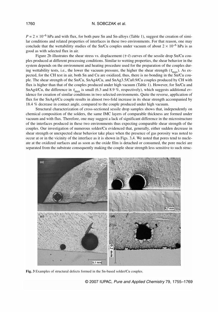
Structural characterization of cross-sectioned sessile drop samples shows that, independently onchemical composition of the solders, the same IMC layers of comparable thickness are formed undervacuum and with flux. Therefore, one may suggest a lack of significant difference in the microstructureof the interfaces produced in these two environments thus expecting comparable shear strength of thecouples. Our investigation of numerous solder/Cu evidenced that, generally, either sudden decrease inshear strength or unexpected shear behavior take place when the presence of gas porosity was noted tooccur at or in the vicinity of the interface as it is shown in Figs. 3,4. We noted that pores tend to nucle-ate at the oxidized surfaces and as soon as the oxide film is detached or consumed, the pore nuclei areseparated from the substrate consequently making the couple shear strength less sensitive to such struc-
N. SOBCZAK et al.
© 2007 IUPAC, Pure and Applied Chemistry 79, 1755–1769
1760
Fig. 3 Examples of structural defects formed in the Sn-based solder/Cu couples.

tural defects. The presence of oxide films contributes also to dissimilar local structure of interfaces suchas discontinuities in the IMC layers, their smaller thickness, compared to the oxide-free regions and innon-flat profile of the Cu/IMC interface. As evidenced in Fig. 4, the above mentioned structural defectslocated at or in the vicinity of the interface are the main source of cracking in thermocycled solder/sub-strate couples thus reducing their reliability.
Additionally, it was noted that these defects do not occur in the solder/Cu couples produced bythe CP procedure, when before contact with the Cu substrate the solder drop is in situ cleaned from itsprimary oxide film directly in vacuum chamber. In order to demonstrate the role of oxide films in theformation of gas porosity in the solder/substrate couples, two tests were done with pure Sn on perfectlyflat and smooth sapphire substrate (roughness Ra = 0.8 Å) under dynamic vacuum of about 2 × 10⁻⁶ hPausing CH and CP procedures. Since the transparent sapphire substrate allows the inspection of the inter-
© 2007 IUPAC, Pure and Applied Chemistry 79, 1755–1769
Wettability and bond strength of solder joints 1761
Fig. 4 Examples of the effects of gas porosity (a–d) and non-flat interface profile accompanied with the formationof non-homogeneous thickness of IMC (e–h) on cracking at or in the vicinity of the interface during thermocycling(TC): (a,c,e,g) before TC, (b,d,f,h) after TC (magnification 200×).
face under magnifications of optical microscopy it was clearly evidenced that gas bubbles are nucleatedat the sapphire substrate in the CH couple while there is no porosity at the interface formed with oxide-free Sn droplet in the CP test.
Note that similar effects of processing conditions and testing procedure on wetting-shear strengthrelationship, caused from the presence of oxide film on a droplet, were reported recently for Al [14] andAl-alloys [17,18] on different ceramics substrates.
Effect of alloying additions
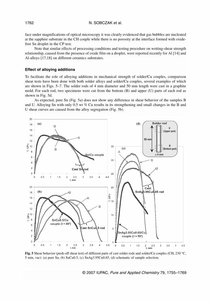
To facilitate the role of alloying additions in mechanical strength of solder/Cu couples, comparisonshear tests have been done with both solder alloys and solder/Cu couples, several examples of whichare shown in Figs. 5–7. The solder rods of 4 mm diameter and 50 mm length were cast in a graphitemold. For each rod, two specimens were cut from the bottom (B) and upper (U) parts of each rod asshown in Fig. 5d.
As expected, pure Sn (Fig. 5a) does not show any difference in shear behavior of the samples Band U. Alloying Sn with only 0.5 wt % Cu results in its strengthening and small changes in the B andU shear curves are caused from the alloy segregation (Fig. 5b).
N. SOBCZAK et al.
© 2007 IUPAC, Pure and Applied Chemistry 79, 1755–1769
1762
Fig. 5 Shear behavior (push-off shear test) of different parts of cast solder rods and solder/Cu couples (CH, 230 °C,5 min, vac): (a) pure Sn, (b) SuCu0.5, (c) SnAg3.95Cu0.65, (d) schematic of sample selection.

Introduction of 3.95 % Ag and 0.65 % Cu produces the alloy of multiphase structure with corre-sponding highest shear strength. However, due to the highest degree of solidification segregation in the
© 2007 IUPAC, Pure and Applied Chemistry 79, 1755–1769
Wettability and bond strength of solder joints 1763
Fig. 6 Shear behavior (push-off shear test) of different parts of cast solder rods and solder/Cu couples withcorresponding optical micrographs of cross-sectioned sessile drop samples under 100× magnification (CH, 230 °C,5 min, vac): (a,c) SnIn5, (b,d) SuIn20.
Fig. 7 Shear behavior (push-off shear test) of cast solder rods and solder/Cu couples (CH, 230 °C, 5 min, vac): (a)Sn/Cu, (b) SnAg4, (c) SnAg3.5Cu0.9, (d) SnAg3.95Cu0.65.
cast rod there is the strongest effect of alloying on shear behavior of dissimilar solidified parts that isevidenced by higher τmax for the bottom than the upper part of cast rod (Fig. 5c).
The reverse relationship takes place in the Sn-In alloys: less alloyed SnIn5 solder (Fig. 6a)demonstrates slightly higher shear strength in the upper part but much bigger difference in the B and Ushear curves, whereas the more alloyed SnIn20 solder (Fig. 6b) has similar shear behavior of the upperand bottom parts but relatively higher τmax in the bottom. From the Sn-In peritectic phase diagram [20],indicating an increase in dissolution of In in Sn with temperature decrease, both alloys should have asingle-phase microstructure resulting in solid solution strengthening of the β-Sn(In) for SnIn5 and theγ-phase for SnIn20. However, due to solidification segregation, the cast SnIn5 rod is more alloyed, andconsequently more strengthened, in its upper part. On the contrary, this part in the SnIn 20 rod presentsthe In-rich γ-phase which has lower strength compared to the Sn-rich γ-phase in the bottom part.Additionally, due to a wide solidification rate, the appearance of shrinkage porosity was noted to occurin the upper part of the SnIn20 rod. The observed effect contributing to the alloy weakening takes placealso in the solder/Cu couples as illustrated in Fig. 6c.
The results reported above demonstrate that the solder shear strength is very sensitive to smallchanges in the materials structure and chemistry. In the case of solder/substrate couples, generally, thedrop-side interface is responsible for the shear behavior of the couple. Therefore, the degree of solderalloying due to the dissolution of the substrate in the solder as well as the structure and thickness ofIMC formed at the interface are the key and competitive factors, influencing the mechanical strength ofa solder/substrate joint.
Under conditions used in this study, the formation of interfacial IMC layers in pure Sn/Cu coupleis not critical at the same time as the dissolution of Cu in Sn results in a slight increase in τmax, com-pared to that of cast Sn rod (Fig. 5a). Alloying with 0.5 % Cu (Figs. 5a,b) and, particularly, with 4 %Ag (Fig. 7a,b) or with both Ag and Cu (Figs. 7c,d) causes further increase in the couple shear strength.On the other hand, for the high content of alloying elements, the shear strength of the couple is muchsmaller compared to that of corresponding cast rod, suggesting that the interface becomes the weakestplace in the joint. Similar relationships are observed in the Sn-In/Cu couples, indicating the coupleweakening due to increase of In content from 5 to 20 % (Figs. 6a,b).
Our observations have shown that alloying additions have the strongest effect on the interfacestructure and their properties. For example, alloying with Cu suppresses the growth of brittle IMC lay-ers (Cu6Sn5 and Cu3Sn). Zn forms the thickest and very brittle IMC layer (Cu5Zn8), which grows in-side the solder drop (the drop/IMC interface is moved toward the drop) that together with a tendency ofZn-containing solders to form porosity at the interface contribute to reliability decrease. Alloying withIn increases the reactivity of the solder/Cu couple, and its consumption for the formation of the In-richIMC phases significantly shifts the droplet composition to a much smaller amount of In while the IMCsformed are relatively less brittle, compared to those formed with other alloying elements. Bi as well asPb do not react with Cu, and thus they do not affect the properties of IMCs formed. However, in theircase, the consumption of Sn for the formation of IMCs with Cu results in shifting chemical composi-tion of the solder to a higher amount of these alloying additions, especially at the solder-side interface.For high Bi content solders, it results in the formation of large Bi grains in the vicinity of the interfacethat may cause low resistance to thermal fluctuations and decreased solder joint reliability as explainedin [21]. These observations are in agreement with the literature data reported for real solder joints (e.g.,[22–26]).
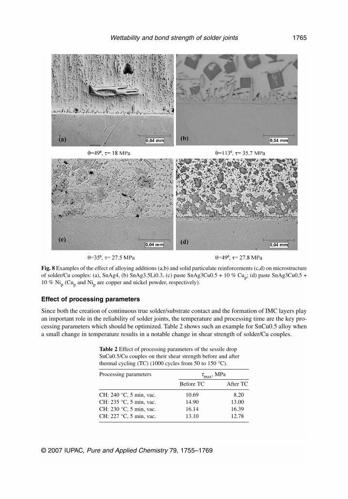
Even a small amount of third alloying element or addition of solid precipitates to a solder werefound to significantly affect reactivity and structure of the solder as well as the type, thickness, and mor-phology of interfaces formed, a few examples of which are shown in Fig. 8. However, more systematicwork is needed to understand how these factors control wetting and mechanical properties of the sol-der/Cu couples.
N. SOBCZAK et al.
© 2007 IUPAC, Pure and Applied Chemistry 79, 1755–1769
1764
Effect of processing parameters
Since both the creation of continuous true solder/substrate contact and the formation of IMC layers playan important role in the reliability of solder joints, the temperature and processing time are the key pro-cessing parameters which should be optimized. Table 2 shows such an example for SnCu0.5 alloy whena small change in temperature results in a notable change in shear strength of solder/Cu couples.
Table 2 Effect of processing parameters of the sessile dropSnCu0.5/Cu couples on their shear strength before and afterthermal cycling (TC) (1000 cycles from 50 to 150 °C).
Processing parameters τmax, MPa
Before TC After TC
CH: 240 °C, 5 min, vac. 10.69 8.20CH: 235 °C, 5 min, vac. 14.90 13.00CH: 230 °C, 5 min, vac. 16.14 16.39CH: 227 °C, 5 min, vac. 13.10 12.78
© 2007 IUPAC, Pure and Applied Chemistry 79, 1755–1769
Wettability and bond strength of solder joints 1765
Fig. 8 Examples of the effect of alloying additions (a,b) and solid particulate reinforcements (c,d) on microstructureof solder/Cu couples: (a), SnAg4, (b) SnAg3.5Li0.3, (c) paste SnAg3Cu0.5 + 10 % Cup; (d) paste SnAg3Cu0.5 +10 % Nip (Cup and Nip are copper and nickel powder, respectively).

The authors suppose also that due to certain methodological problems with the temperaturemeasurements in the discussed low-temperature range of Sn-based solders when fast heating and cool-ing are required, there is no sureness that the contact angle values given in the literature always corre-spond to a true temperature. Furthermore, chemical reactions, accompanying the formation of IMCphases, may cause heat release and signify an additional factor for temperature fluctuation in the cou-ple, as reported in [27].
Effect of testing procedure used for characterization of interfacial strength
In order to identify the effect of testing procedure, two sets of experiments were performed. The firstone was focused on comparison studies of two halves of the same sessile drop couples using two typesof testing machines with two corresponding different designs of holders for shearing sessile droplets.These tests show only a maximum 2 % difference in the shear strength measurements, thus suggestinga good repeatability and reliability of the results of push-off shear tests.
The second set of experiments was done by push-out shear test using different inner diameters ofthe Cu rings (Fig. 1d); those most representative results are shown in Table 3 and Fig. 8. For the Sn/Cuand SnPb40/Cu couples characterized by relatively thin layers of IMC, the size of the loading punchhas no effect on the shear strength of these samples. However, their shear strength is almost two-foldhigher than that of the solidified sessile drop samples examined by the push-off shear test. This effectmay be caused by dissimilar testing conditions due to two effects taking place during loading and shear-ing of the solder part in the push-out shear test: (1) higher roughness of unpolished (only machined)inner surface of the Cu ring, (2) high ductility of Sn and SnPb40 alloys resulting in plastic deformationaccompanying with additional friction (solder extrusion through a hole in the Cu ring).
Table 3 Effect of testing procedure on shear strength of solder/Cu couples (CH: 230 °C, 5 min, flux).
Solder SD samples Push-out samples (φ5 mm)
θ, ° τmax, MPa τmax, MPa (push-out shear test)
(push-off shear test) d = 4.92 mm d = 4.95 mm d = 5 mm
Sn 47 ± 4 18.55 ± 2.1 34.43 ± 0.03 34.80 ± 0.8 37.51 ± 2.37SnPb40 16 ± 5 7.3 ± 4.4 51.13 ± 1.1 50.68 ± 0.38 50.75 ± 0.45SnZn13.5 53 ± 4 26.71 ± 3.65 16.39 ± 2.2 29.65 ± 0.54 46.43 ± 3.52
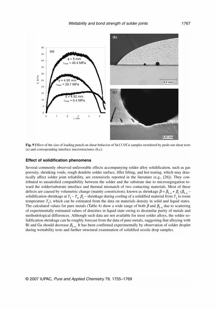
For such alloys as SnZn13.5 (Fig. 9a), which are characterized by relatively low plasticity andhigh reactivity with the Cu substrate (evidenced by the formation of almost two-fold thicker IMC layerthan that formed with pure Sn and SnPb40), the punch diameter has a significant effect on the push-outshear strength and τmax measured with d = 4.95 mm is comparable to that of push-off shear test on thesolidified sessile drop sample. This effect is caused by a relatively thick IMC layer that is growing in-side the solder and has nonhomogeneous thickness due to a local non-wetting accompanied by gas bub-ble nucleation (Fig. 9b), all contributing to decreased resistance to shear loading.
N. SOBCZAK et al.
© 2007 IUPAC, Pure and Applied Chemistry 79, 1755–1769
1766
Effect of solidification phenomena
Several commonly observed unfavorable effects accompanying solder alloy solidification, such as gasporosity, shrinking voids, rough dendrite solder surface, fillet lifting, and hot tearing, which may dras-tically affect solder joint reliability, are extensively reported in the literature (e.g., [26]). They con-tributed to unsatisfied compatibility between the solder and the substrate due to microsegregation to-ward the solder/substrate interface and thermal mismatch of two contacting materials. Most of thesedefects are caused by volumetric change (mainly constriction), known as shrinkage β = βl–s + βs (βl–s –solidification shrinkage at Tl − Ts, βs – shrinkage during cooling of a solidified material from Ts to roomtemperature Tr), which can be estimated from the data on materials density in solid and liquid states.The calculated values for pure metals (Table 4) show a wide range of both β and βl–s due to scatteringof experimentally estimated values of densities in liquid state owing to dissimilar purity of metals andmethodological differences. Although such data are not available for most solder alloys, the solder so-lidification shrinkage can be roughly forecast from the data of pure metals, suggesting that alloying withBi and Ga should decrease βl–s. It has been confirmed experimentally by observation of solder dropletduring wettability tests and further structural examination of solidified sessile drop samples.
© 2007 IUPAC, Pure and Applied Chemistry 79, 1755–1769
Wettability and bond strength of solder joints 1767
Fig. 9 Effect of the size of loading punch on shear behavior of Sn13.5/Cu samples reordered by push-out shear tests(a) and corresponding interface microstructures (b,c).
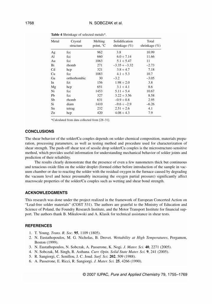
Table 4 Shrinkage of selected metals*.
Metal Crystal Melting Solidification Totalstructure point, °C shrinkage (%) shrinkage (%)
Ag fcc 962 3.8 10.99Al fcc 660 6.0 ÷ 7.14 11.66Au fcc 1063 5.1 ÷ 5.47 11Bi rhomb 271 –3.35 ÷ –3.32 –2.73Cd hcp 321 3.8 ÷ 4.7 7.18Cu fcc 1083 4.1 ÷ 5.3 10.7Ga orthorhombic 30 –3.2 –3.05In fct 156 1.98 ÷ 2.0 3.8Mg hcp 651 3.1 ÷ 4.1 8.6Ni fcc 1453 5.11 ÷ 5.4 10.67Pb fcc 327 3.22 ÷ 3.56 8.58Sb rhomb 631 –0.9 ÷ 0.8 2.95Si diam 1410 –9.6 ÷ –2.9 –6.26Sn tetrag 232 2.51 ÷ 2.6 4.1Zn hcp 420 4.08 ÷ 4.3 7.9
*Calculated from data collected from [28–31].
CONCLUSIONS
The shear behavior of the solder/Cu couples depends on solder chemical composition, materials prepa-ration, processing parameters, as well as testing method and procedure used for characterization ofshear strength. The push-off shear test of sessile drop solder/Cu couples is the microstructure-sensitivemethod, which provides useful information for understanding mechanical behavior of solder joints andprediction of their reliability.
The results clearly demonstrate that the presence of even a few nanometers thick but continuousand tenacious oxide film on the solder droplet (formed either before introduction of the sample in vac-uum chamber or due to reacting the solder with the residual oxygen in the furnace caused by degradingthe vacuum level and hence presumably increasing the oxygen partial pressure) significantly affectmacroscale properties of the solder/Cu couples such as wetting and shear bond strength.
ACKNOWLEDGMENTS
This research was done under the project realized in the framework of European Concerted Action on“Lead-free solder materials” (COST 531). The authors are grateful to the Ministry of Education andScience of Poland, the Foundry Research Institute, and the Motor Transport Institute for financial sup-port. The authors thank B. Mikulowski and A. Klasik for technical assistance in shear tests.
REFERENCES
1. T. Young. Trans. R. Soc. 95, 1109 (1805).2. N. Eustathopoulos, M. G. Nicholas, B. Drevet. Wettability at High Temperatures, Pergamon,
Boston (1999).3. N. Eustathopoulos, N. Sobczak, A. Passerone, K. Nogi. J. Mater. Sci. 40, 2271 (2005).4. N. Sobczak, M. Singh, R. Asthana. Curr. Opin. Solid State Mater. Sci. 9, 241 (2005). 5. R. Sangiorgi, C. Senillou, J. C. Joud. Surf. Sci. 202, 509 (1988).6. A. Passerone, E. Ricci, R. Sangiorgi. J. Mater. Sci. 25, 4266 (1990).
N. SOBCZAK et al.
© 2007 IUPAC, Pure and Applied Chemistry 79, 1755–1769
1768

7. P. Protsenko, A. Terlain, M. Jeymond, N. Eustathopoulos. J. Nucl. Mater. 307–311, 1396 (2002).8. N. Sobczak, J. Sobczak, B. Mikulowski, A. Wojciechowski, R. Nowak, A. Kudyba, P. Darlak. J.
Mater. Sci. 40, 2547 (2005).9. W. H. Sutton. Report R-64 SD44, GE Space Sciences Lab, USA, 1964.
10. M. Nicholas. J. Mater. Sci. 3, 571 (1968). 11. M. Nicholas, R. R. D. Forgan, D. M. Poole. J. Mater. Sci. 3, 9 (1968). 12. S. M. Wolf, A. P. Levitt, J. Brown. Chem. Eng. Prog. 62, 74 (1966).13. N. Sobczak, M. Ksiazek, W. Radziwill, L. Stobierski, B. Mikulowski. Trans. JWRI 30, 125
(2001).14. N. Sobczak. Kompozyty 3, 301 (2003).15. N. Sobczak, K. Nogi, H. Fujii, T. Matsumoto, K. Tamada, R. Asthana. In Joining of Advanced &
Specialty Materials, J. N. Indacochea et al. (Eds.), pp. 108–115, ASM International, MaterialsPark, OH (2003).
16. N. Sobczak, R. Asthana, M. Ksiazek, W. Radziwill, B. Mikulowski. Metall. Mater. Trans. A 35,911 (2004).
17. N. Sobczak, R. Asthana. Ceram. Trans. 158, 3 (2005).18. N. Sobczak, R. Asthana, W. Radziwill, R. Nowak, A. Kudyba. Bull. Pol. Acad. Sci. (2007).
Accepted for publication.19. R. Asthana, S. T. Mileiko, N. Sobczak. Bull. Pol. Acad. Sci. 54, 147 (2006).20. T. B. Massalski. Binary Phase Diagrams, Vol. 3, The Minerals Information Society (1990).21. C.-W. Hwang, K. Suganuma, E. Saiz, A. P. Tomsia. Trans. JWRI 30, 167 (2001).22. K. N. Tu, A. M. Gusak, M. Li. J. Appl. Phys. 93, 1335 (2003).23. J. S. Hwang. Environment-Friendly Electronics: Lead-free Technology, Electrochemical
Publications (2001).24. A. Hirose, H. Yanagawa, E. Ide, K. F. Kobayashi. Sci. Technol. Adv. Mater. 5, 267 (2004).25. K. J. Ronka, F. J. van Loo, J. K. Kivilahti. Scripta Mater. 37, 1575 (1997).26. K. J. Puttlitz, K. A. Stalter. Handbook of Lead-free Solder Technology for Microelectronic
Assemblies, Marcel Dekker, New York (2004).27. V. M. Perevertailo, S. M. Samokhin, O. G. Kulik, M. A. Opanasenko. J. Superhard Mater. 24,
2832 (2002).28. J. Campbell. Castings, Butterworth-Heinemann, London (1997).29. A. R. Ubbelohde. The Molten State of Matter, John Wiley, New York (1978). 30. C. J. Smithells. Metals, Butterworth, London (1976).31. P. P. Arsentiev, L. A. Koledov. Metallicheskie Rasplavy i Ich Svoistva, Metallugia, Moscow
(1976).
© 2007 IUPAC, Pure and Applied Chemistry 79, 1755–1769
Wettability and bond strength of solder joints 1769