Embed Size (px)
Citation preview

Facebook PCIe Retimer Card
Rev 1.1
Author:
Chris Petersen, Hardware System Engineer, Facebook
Clark Shao, Hardware Engineer, Facebook

© 2017 Facebook.
As of June 12, 2017, the following persons or entities have made this Specification available under the Open Web Foundation Final Specification Agreement (OWFa 1.0), which is available at: http://www.openwebfoundation.org/legal/the-owf-1-0-agreements/owfa-1-0:
Facebook, Inc.
You can review the signed copies of the Open Web Foundation Agreement Version 1.0 for this Specification at http://opencompute.org/licensing/, which may also include additional parties to those listed above.
Your use of this Specification may be subject to other third party rights. THIS SPECIFICATION IS PROVIDED "AS IS." The contributors expressly disclaim any warranties (express, implied, or otherwise), including implied warranties of merchantability, noninfringement, fitness for a particular purpose, or title, related to the Specification. The entire risk as to implementing or otherwise using the Specification is assumed by the Specification implementer and user. IN NO EVENT WILL ANY PARTY BE LIABLE TO ANY OTHER PARTY FOR LOST PROFITS OR ANY FORM OF INDIRECT, SPECIAL, INCIDENTAL, OR CONSEQUENTIAL DAMAGES OF ANY CHARACTER FROM ANY CAUSES OF ACTION OF ANY KIND WITH RESPECT TO THIS SPECIFICATION OR ITS GOVERNING AGREEMENT, WHETHER BASED ON BREACH OF CONTRACT, TORT (INCLUDING NEGLIGENCE), OR OTHERWISE, AND WHETHER OR NOT THE OTHER PARTY HAS BEEN ADVISED OF THE POSSIBILITY OF SUCH DAMAGE.
CONTRIBUTORS AND LICENSORS OF THIS SPECIFICATION MAY HAVE MENTIONED CERTAIN TECHNOLOGIES THAT ARE MERELY REFERENCED WITHIN THIS SPECIFICATION AND NOT LICENSED UNDER THE OWF CLA OR OWFa. THE FOLLOWING IS A LIST OF MERELY REFERENCED TECHNOLOGY: INTELLIGENT PLATFORM MANAGEMENT INTERFACE (IPMI), I2C TRADEMARK OF PHILLIPS SEMICONDUCTOR. IMPLEMENTATION OF THESE TECHNOLOGIES MAY BE SUBJECT TO THEIR OWN LEGAL TERMS.


1 Revision History Version Date Name Description
V0.1 December 2016 Chris Petersen Initial release
V0.2 1/2/2017 Clark Shao Adding details based on the framework created in V0.1.
V0.3 1/26/2017 Clark Shao
Chris Petersen
5.1 Block diagram section updated
5.3.1 Retimer section updated
5.3.3 USB hub section updated
5.6 PCIe Mini-SAS HD Connector Pinout updated
5.7 USB Connector section merged into 5.3.3
5.9 I2C Connection updated, add FRUID format
Adding a section to include differences between different versions of retimer cards
Also modified formats throughout the spec.
V0.4 2/2/2017 Clark Shao
Koh Yew Thoon
Correcting a few descriptions based on Koh Yew’s feedback.
Adding future support for SRIS in section 5.1
V0.5 3/5/2017 Clark Shao Adding clarification on SRIS future support in sec 5.1 and 5.2
V0.6 3/25/2017 Clark Shao
Eric YH Yang
Adding “EEPROM for FRUID” in 5.2
Updating picture of retimer card with PVT version in 5.3.3
Adding notes that golden finger pin B11/B30 not used in Facebook’s retimer card in 5.5
Updating MiniSAS HD cable table with Amphenol 1.5m cable added, removing Molex 2m cable, updating Amphenol 520/350mm cables’ MPN in 5.6
Adding detail dimensions for retimer card in 8.1
V0.7 4/3/2017 Chris Petersen Thermal environment and final cleanup
V1.0 4/4/2017 Clark Shao R.H. requirement from 90% to 85% in 7.1.4

Description on altitude from 1000m to 2000m in 10.1
Some more cleanup
V1.1 6/10 Clark Shao Updated 7.1.2 with cold aisle temperature
Added 7.1.5 with airflow recommendation
2 Scope This specification describes the design and design requirements for a PCIe add-in card that converts an internal PCIe connection to an external PCIe connection.
3 Contents 1 Revision History ..................................................................................................................................................... 4
2 Scope .......................................................................................................................................................................... 5
3 Contents .................................................................................................................................................................... 6
4 Overview ................................................................................................................................................................... 8
5 Physical Spec ........................................................................................................................................................... 8
5.1 Block Diagram ................................................................................................................................................ 8
5.2 Requirements ................................................................................................................................................. 9
5.3 Key components ........................................................................................................................................... 9
5.3.1 Retimer ........................................................................................................................................................ 9
5.3.2 Clock Buffer .............................................................................................................................................. 11
5.3.3 USB Hub and USB Connection ........................................................................................................... 12
5.4 PCB Stack-up ................................................................................................................................................. 14
5.5 PCIe Edge Connector Pinout ................................................................................................................... 14
5.6 PCIe Mini-SAS HD Connector Pin Definition ..................................................................................... 16
5.7 PCIe Bi-furcation Control ......................................................................................................................... 18
5.8 LEDs ................................................................................................................................................................. 19
5.9 I2C Connection............................................................................................................................................. 19
6 Retimer Cards in Different Platforms .......................................................................................................... 21
6.1 Changes from a JBOF Retimer Card to a JBOG Retimer Card....................................................... 21
7 Thermal requirements and design ................................................................................................................ 22
7.1 Data Center Environmental Conditions ............................................................................................. 22
7.1.1 Location of Data Center/Altitude .................................................................................................... 22
7.1.2 Cold-Aisle temperature ........................................................................................................................ 22
7.1.3 Cold-Aisle Pressurization .................................................................................................................... 22
7.1.4 R.H ................................................................................................................................................................ 22
7.1.5 Air Flow Recommendation ................................................................................................................. 22
7.2 Heatsink design ........................................................................................................................................... 23
8 Mechanical ............................................................................................................................................................. 23
8.1 Form factor ................................................................................................................................................... 23
8.2 PCB Color ....................................................................................................................................................... 24
9 Labels and Markings ........................................................................................................................................... 25
10 Environmental and Regulations ................................................................................................................ 25
10.1 Environmental Requirements ............................................................................................................... 25
10.2 Vibration & Shock ....................................................................................................................................... 26
10.3 Regulations ................................................................................................................................................... 26

11 Prescribed Materials ...................................................................................................................................... 26
11.1 Disallowed Components .......................................................................................................................... 26
11.2 Capacitors & Inductors ............................................................................................................................. 26
11.3 Component De-rating ............................................................................................................................... 27

4 Overview This specification describes the design of a PCIe retimer card that plugs into a PCIe standard x16 slot, re-drives the PCIe signals to external mini-SAS HD connectors (4 total), buffers a single PCIe clock, and provides sideband USB and I2C interfaces. This card allows a traditional server to connect via external PCIe cables to another server or storage chassis that has the same external PCIe connection.
5 Physical Spec 5.1 Block Diagram
Figure 1 shows the block diagram of the retimer card.
The upstream port of the retimer is connected to the host through a standard PCIe card edge connector with x16 PCIe lanes and sideband signals. The downstream port of the retimer is connected to four MiniSAS HD connectors, each of which has x4 PCIe lanes.
A clock buffer is used to convert one pair of PCIe REFCLK signals from the host to five pairs of REFCLK signals to the retimer chip and MiniSAS HD connectors. Common clock with SSC enabled architecture is used on the JBOF version of retimer card. SRNS (Separate Reference Clocks with No SSC) is used on the JBOG version of retimer card. For detailed differences between the JBOF version and the JBOG version of the retimer card, please refer to section 11.
In the future, the goal is to support SRIS so there will not be REFCLK pairs going through the cable. Currently as of year 2017, both JBOF and JBOG retimer cards will not support SRIS.
The input of the USB hub can be either from a Mini-USB connector on the retimer card that is connected to the server board using a USB cable, or from the PCIe edge connector if the host supports USB sideband signals through the edge connector.
The I2C signals going into the four MiniSAS HD connectors can be either from a 1-to-4 I2C Mux or directly from the edge connector.
A buffer is used to convert the reset from the host to the four resets going into the four MiniSAS HD connectors.
The “retimer card” refers to the board while “retimer” refers to the retimer ASIC (89HT0832PZCHLG8) within this spec.

Figure 1 PCIe Retimer Card Block Diagram
5.2 Requirements Key requirements are:
• The card should be compliant with PCIe 3.0 CEM spec. • The card should have a retimer to improve the signal integrity across long cables
and/or PCB traces. • The card should be able to transmit all the sideband signals required from the
host to all the downstream devices in different configurations such as 1x16, 2x8 or 4x4 mode.
• There should be on-board options to easily switch among different configuration modes 1x16, 2x8 and 4x4.
• BOM options should be reserved to support MiniSAS HD connector pin definition according to PCI Express External Cabling spec.
• SRNS and common clock with SSC enabled need to be supported as of year 2017. SRIS shall be supported in the future.
• An EEPROM is needed to store the FRUID for the retimer card.
5.3 Key components 5.3.1 Retimer
The retimer card uses a PCIe retimer with its upstream x16 lanes connected to the host though the PCIe edge connector, and downstream x16 lanes connected to four MiniSAS HD connectors, which are connected to a JBOF or JBOG or other external system through 2x x8 Mini SAS HD cables with side-band signals. The PCIe retimer should support the following key features:
• Ability to support up to 8GT/s • Ability to bi-furcate to up to four x4 PCIe lanes • Ability to log and report PCIe Rx eye openings • Ability to tune PCIe equalization settings on a per port basis

The recommended device is IDT’s 89HT0832PZCHLG8. The mapping of the lanes from the host to the retimer upstream port and from the retimer downstream port to MiniSAS HD connectors are user specific and should be implemented by considering SI performance, routing convenience and easy cable connection. Cable connections need to be planned at the same time as the designer plans the PCIe routing. For example, when 2x x8 cables are used, connector A/ B and C/D are bundled together respectively. Consequently, the cable connection and routing will be different than using either four x4 cables or one x16 cable.
Figure 2 shows the routing strategy of a retimer card used in the JBOF system:
• No lane reversal from the PCIe edge connector to the retimer. • Lane reversal is implemented for each group of x4 lanes of the retimer downstream
port and each MiniSAS HD connector for routing convenience. • No lane reversal between each group of x4 lanes of the PCIe switch upstream port
and each MiniSAS HD connector. • Connector A, B, C, D of the retimer card needs to be connected to connector A, B, C, D
of JBOF respectively to ensure the PCIe connection between retimer and PCIe switch is always lane reversed in all configurations (1x16, 2x8 and 4x4).
User does not have to use this lane reversal approach but can define their own lane mapping and cable connection strategy.
Conn A
Conn B
Conn C
Conn D
0123
0123
0123
0123
Lane 0 à 15
89HT0832
1514131211109876543210
15
0
B1 B82
Top View of Retimer Card
Downstream Upstream
To Host
Conn D
Conn C
Conn B
Conn A
0123
0123
0123
0123
PCIe Switch
To Storage System
1514131211109876543210
Storage System(JBOF)
MiniSASHD Cables
Figure 2 Retimer Card PCIe Routing and Cable Connection Strategy with a JBOF
To make sure the cable connection is correct, labels “A”, “B”, “C” and “D” are added on the retimer card and they should be added on the system on the other end of the cable to make installation straightforward. The labels shall be placed on the bottomside of the card so they are easily visible when the card is installed in the server. The labels are shown below on the left side of the retimer card in Figure 3.

Figure 3 Connector Labels on Retimer Card
5.3.2 Clock Buffer
The clock buffer is the device used to provide 5 differential pairs of REFCLK to the retimer and the four MiniSAS HD connectors. It uses the REFCLK from the host as the input and presents signals from each cable as the enable signal for each pair of REFCLK signals.
The recommended device is IDT’s 9DBV0631BKLF.
Refer to the figure below for the clock topology of the retimer card.
Figure 4 Retimer Card Clock Topology

5.3.3 USB Hub and USB Connection
On the retimer card, there are two options to connect USB from the host to the retimer card: one through a USB cable to a mini-USB connector on the retime card, and the other one through PCIe edge connector. A USB hub is also used to provide a USB interface between the host and each of the MiniSAS HD connectors. A mini-USB type B connector is provided to allow for systems that do not have the USB connection routed through the PCIe edge connector. A BOM option using zero ohm resistors is provided to choose either connection path.
The USB interface will be used as the primary communication interface between the host and the JBOF BMC.
USB2514B is the device being used as the USB hub in the JBOF retimer card. The USB connection block diagram is shown below in Figure 5.
Retimer Card
Mini-USB Type B
connectorMini-sas HD
Mini-sas HD
Mini-sas HD
Mini-sas HD
USB hub
A32: USB_DPA33: USB_DN
O Ohm
O Ohm
From Host SupportingUSB Cable Connection
From Host SupportingUSB Golden Finger
Connection
Figure 5 Retimer Card USB Connection Block Diagram
The mini-USB type B connector drawing and its location on the retimer card are shown below as a reference.

Figure 6 Drawing of the Mini-USB Type B Connector
Figure 7 Location of the Mini-USB Type B Connector on a Retimer Card

5.4 PCB Stack-up The card is using an 8 layer stack-up as shown below. For PCB material, TU863-VLP or NPG171-VLP or materials with a similar Df at 1GHz is recommended.
Figure 8 PCIe Retimer Card Stack-up
5.5 PCIe Edge Connector Pinout The edge connector pin-out is shown in the table below and aligns with the PCI Express® Card Electromechanical Specification revision 3.0.
Please note that A7 and A8 are customized pins connected to an EEPROM on the card that’s used to store the FRUID so the host can use it to identify the specific retimer card (refer to section 5.9).
Also, A32 and A33 are customized pins used for the USB connection from host to the downstream devices. B11 and B30 are not used in Facebook’s retimer card.
Pin Side B Golden Finger Side A Golden Finger
# Name Name
1 +12v PRSNT#1
2 +12v +12v
3 +12v +12v
4 GND GND
5 SMCLK NC
6 SMDAT NC
7 GND SMBCLK_PCH
8 +3.3v SMBDAT_PCH
9 NC +3.3v
10 P3V3_AUX +3.3v
11 WAKE# PERST#
Mechanical Key
12 SMB_ALERT_N GND
13 GND REFCLK1+
Glass/Copper Style Df(1G)Cu oz Wiwynn Wiwynn
0.5 3.4 0.025Top 0.5 oz+plating 2.1
3 3.9 0.009L2 1 oz 1.3
4 3.9 0.009L3 1 oz 1.3
16 4.5 0.009L4 1 oz 1.3
4 3.9 0.009L5 1 oz 1.3
16 4.5 0.009L6 1 oz 1.3
4 3.9 0 0.009L7 1 oz 1.3
3 3.9 0 0.009Bottom 0.5 oz+plating 2.1
0.5 3.4 0 0.025mil 63mm 1.60
Layer Thickness
Core
Mask
GNDPrepregSignalMask
Thickness requirement: 1.6 +6.5% / -10% mm
SignalCore
SignalPrepreg
Er
SignalPrepreg
GND
Prepreg
GNDCoreGND

14 PETp(0) REFCLK1-
15 PETn(0) GND
16 GND PERp(0)
17 NC PERn(0)
18 GND GND
19 PETp(1) RSVD
20 PETn(1) GND
21 GND PERp(1)
22 GND PERn(1)
23 PETp(2) GND
24 PETn(2) GND
25 GND PERp(2)
26 GND PERn(2)
27 PETp(3) GND
28 PETn(3) GND
29 GND PERp(3)
30 PWR_BRK# PERn(3)
31 PRSNT#2-3 GND
32 GND USB2.0+P
33 PETp(4) USB2.0+N
34 PETn(4) GND
35 GND PERp(4)
36 GND PERn(4)
37 PETp(5) GND
38 PETn(5) GND
39 GND PERp(5)
40 GND PERn(5)
41 PETp(6) GND
42 PETn(6) GND
43 GND PERp(6)
44 GND PERn(6)
45 PETp(7) GND
46 PETn(7) GND
47 GND PERp(7)
48 PRSNT#2-4 PERn(7)
49 GND GND
50 PETp(8) RSVD
51 PETn(8) GND
52 GND PERp(8)
53 GND PERn(8)
54 PETp(9) GND
55 PETn(9) GND
56 GND PERp(9)

57 GND PERn(9)
58 PETp(10) GND
59 PETn(10) GND
60 GND PERp(10)
61 GND PERn(10)
62 PETp(11) GND
63 PETn(11) GND
64 GND PERp(11)
65 GND PERn(11)
66 PETp(12) GND
67 PETn(12) GND
68 GND PERp(12)
69 GND PERn(12)
70 PETp(13) GND
71 PETn(13) GND
72 GND PERp(13)
73 GND PERn(13)
74 PETp(14) GND
75 PETn(14) GND
76 GND PERp(14)
77 GND PERn(14)
78 PETp(15) GND
79 PETn(15) GND
80 GND PERp(15)
81 PRSNT#2-6 PERn(15)
82 RSVD GND
Table 1 Golden Finger Pin Definition
5.6 PCIe Mini-SAS HD Connector Pin Definition A customized MiniSAS HD connector (SFF-8644) pin definition is used in Facebook retimer card, which is different from the PCIe SIG’s external cabling spec.
The table below shows the MiniSAS HD fixed-side connector pin definition from the PCI Express® External Cabling Specification 3.0, REV0.7.
Row\Col
9 8 7 6 5 4 3 2 1
D GND PETn2 PETp2 GND PETn1 PETp1 GND MGTPWR PWR
C GND PETn3 PETp3 GND PETn0 PETp0 GND CMISDA CMISCL
B GND PERn2 PERp2 GND PERn1 PERp1 GND CBLPRSNT# PWR
A GND PERn3 PERp3 GND PERn0 PERp0 GND CINT# CADDR
Table 2 MiniSAS HD Connector Pin Definition from PCIe External Cabling Spec

The differences between Facebook’s pin definition and the PCIe SIG’s pin definition is listed in the table below.
PCIe SIG’s Spec (Draft)
Facebook Customized Spec
A1 CADDR REF_CLK_P
A2 CINT# REF_CLK_N
B1 PWR PERST#
D1 PWR USB_DN
D2 MGTPWR USB_DP
Table 3 Pin Definition differences between Facebook Spec and PCIe SIG Spec
BOM options are reserved on the retimer card to enable the PCIe SIG pinout as needed. Details are shown below:
• P3V3 is connected to A9/A10 of the PCIe edge connector, P3V3_AUX is connected to B10 of PCIe edge connector.
• The default BOM is to enable Facebook’s pin definition. Noted that INT# from PCA9544 will be connected to pin B12 of the PCIe edge connector.
Figure 9 Design for Compatibility between Facebook and PCIe SIG’s Pin Definition
These BOM options to enable the PCIe SIG pinout is only for functional check and not fully compatible with the latest external cable specification “PCI_Express_External_Cabling_R3.0_v0.7_TS_11092016_NCB”. For example, the USB_DN signal is a signal with 5 mil trace width instead of being routed as a wider power trace.
The table below shows some of the cable examples that are being with Facebook’s retimer card.

Supplier Cable Length Type Part Number
Amphenol 520mm X8 NEEECA-Q107
Amphenol 350mm X8 NEEECA-Q106
JPC 520mm X8 P4103B250550-1
JPC 350mm X8 P4103B250400-1
Molex 1.5M X8 1110752201
Amphenol 1.5M X8 NEETCT-F402
Table 4 MiniSAS HD Cable Examples
5.7 PCIe Bi-furcation Control The retimer card supports the ability to connect to one, two, three, or four PCIe endpoints. As a result, the card needs to provide both the ability to set the retimer bi-furcation setting as well as allow the BIOS to detect the current setting. To enable this, a set of jumpers is provided to change between 1x x16, 2x x8, or 4x x4.
Logic will also be needed to control the retimer strap pins (Merge[0..2]) to set the retimer to the required mode.
The table and figure below show an example of how to configure the retimer card to different bi-furcation settings. The jumper location in rows “CN4/CN5/CN6” is user specific depending on the circuit implementation.
Net Name(Pin # of Golden Finger) 4x4 2x8 1x16
GF_PRSNT3_N(b31) 0 1 0
GF_PRSNT4_N(b48) 0 0 0
GF_PRSNT6_N(b81) 0 0 1
CN4 2-3 1-2 2-3
CN5 2-3 2-3 2-3
CN6 2-3 2-3 1-2
Merge[0] 0 1 x
Merge[1] 0 1 X
Merge[2] 0 0 1
Table 5 Logic Table and Jumper Location for Different Bi-furcation Settings

Figure 10 Retimer Card Bi-furcation Configuration Circuit
5.8 LEDs The card has one blue LED to indicate that the card has powered on successfully.
1.8V Good and 1.0V Good
1.8V Low or 1.0V Low
LED1 ON OFF
Table 6 Power Good Indicator LED
The card also has 3x green LEDs to indicate the current PCIe bi-furcation setting as shown in the table below.
4x4 2x8 1x16
LED19 ON OFF OFF
LED18 OFF ON OFF
LED17 OFF OFF ON
Table 7 Bi-Furcation Setting Indicator LED
5.9 I2C Connection There are several I2C devices on the retimer card and they are listed below:
• EEPROM to store the retimer chip configuration file • The clock buffer • IO Expander to indicate to the host which connector’s PRSNT# is asserted • I2C Mux to connect the I2C from host to MiniSAS HD connectors(Optional) • EEPROM to store the FRUID of the retimer card

The block diagram of the retimer card’s I2C topology is shown below.
Different power domains are used to pull up the I2C lines for different devices.
Isolation circuits should be used to isolate leakage from either the host to downstream devices or from downstream devices to the host.
Figure 11 I2C Topology
For the EEPROM used to store FRUID(Field Replaceable Unit ID), a controller(e.g. PCH) from host would be needed to access it and the format of the contents of the FRUID should follow the IPMI Platform Management FRU Information Storage Definition v1.0.
The contents of the FRUID are defined in the table below. The table only defines the minimum number of required bytes, but if longer fields are needed adding additional bytes is acceptable.
Name Minimum byte count
Value Name
Board Mfg Date 3 Date the board was manufactured Board Mfg Date
Board Mfg 6 Manufacturer Board Mfg
Board Product 19 “PCIe Retimer Card” Board Product
Board Serial Number 11 Supplier defined serial number Board Serial Number
Board Part Number 11 Supplier defined part number Board Part Number
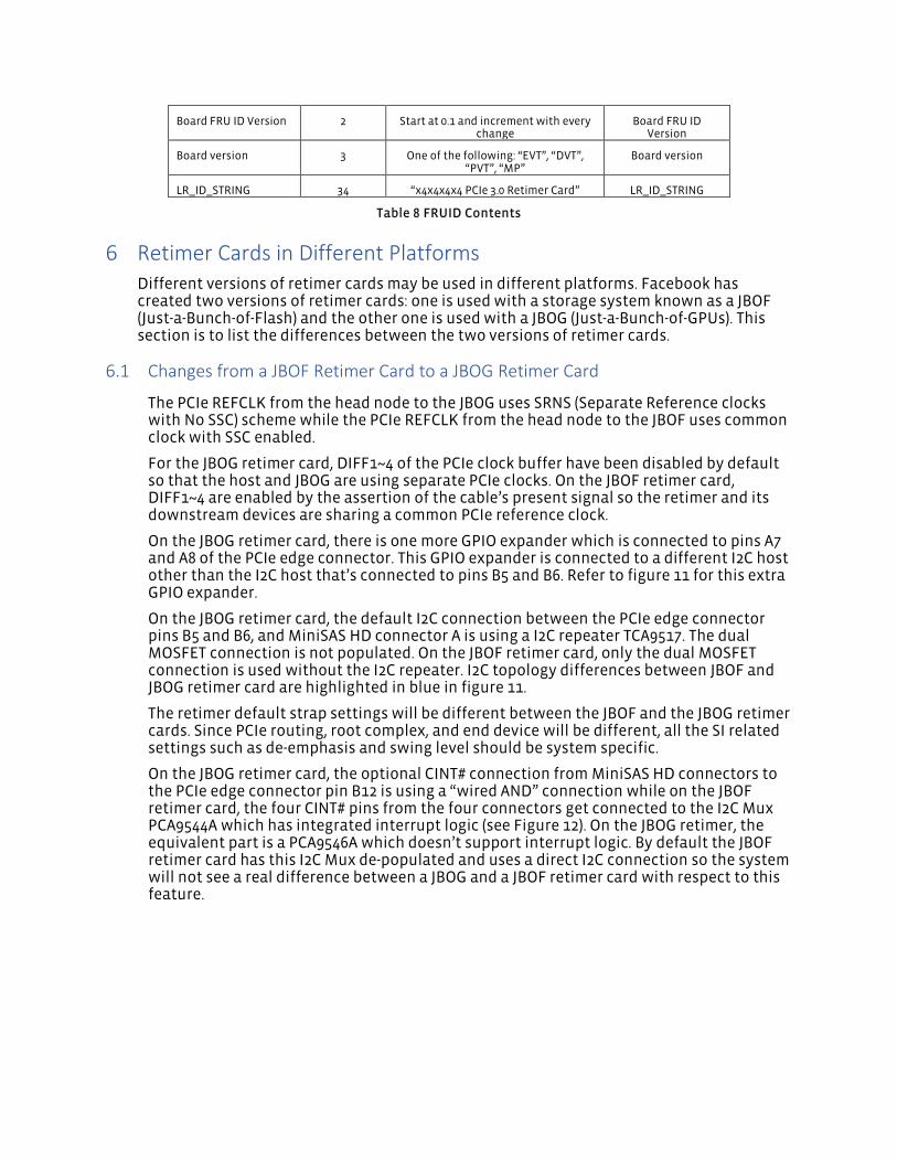
Board FRU ID Version 2 Start at 0.1 and increment with every change
Board FRU ID Version
Board version 3 One of the following: “EVT”, “DVT”, “PVT”, “MP”
Board version
LR_ID_STRING 34 “x4x4x4x4 PCIe 3.0 Retimer Card” LR_ID_STRING
Table 8 FRUID Contents
6 Retimer Cards in Different Platforms Different versions of retimer cards may be used in different platforms. Facebook has created two versions of retimer cards: one is used with a storage system known as a JBOF (Just-a-Bunch-of-Flash) and the other one is used with a JBOG (Just-a-Bunch-of-GPUs). This section is to list the differences between the two versions of retimer cards.
6.1 Changes from a JBOF Retimer Card to a JBOG Retimer Card
The PCIe REFCLK from the head node to the JBOG uses SRNS (Separate Reference clocks with No SSC) scheme while the PCIe REFCLK from the head node to the JBOF uses common clock with SSC enabled.
For the JBOG retimer card, DIFF1~4 of the PCIe clock buffer have been disabled by default so that the host and JBOG are using separate PCIe clocks. On the JBOF retimer card, DIFF1~4 are enabled by the assertion of the cable’s present signal so the retimer and its downstream devices are sharing a common PCIe reference clock.
On the JBOG retimer card, there is one more GPIO expander which is connected to pins A7 and A8 of the PCIe edge connector. This GPIO expander is connected to a different I2C host other than the I2C host that’s connected to pins B5 and B6. Refer to figure 11 for this extra GPIO expander.
On the JBOG retimer card, the default I2C connection between the PCIe edge connector pins B5 and B6, and MiniSAS HD connector A is using a I2C repeater TCA9517. The dual MOSFET connection is not populated. On the JBOF retimer card, only the dual MOSFET connection is used without the I2C repeater. I2C topology differences between JBOF and JBOG retimer card are highlighted in blue in figure 11.
The retimer default strap settings will be different between the JBOF and the JBOG retimer cards. Since PCIe routing, root complex, and end device will be different, all the SI related settings such as de-emphasis and swing level should be system specific.
On the JBOG retimer card, the optional CINT# connection from MiniSAS HD connectors to the PCIe edge connector pin B12 is using a “wired AND” connection while on the JBOF retimer card, the four CINT# pins from the four connectors get connected to the I2C Mux PCA9544A which has integrated interrupt logic (see Figure 12). On the JBOG retimer, the equivalent part is a PCA9546A which doesn’t support interrupt logic. By default the JBOF retimer card has this I2C Mux de-populated and uses a direct I2C connection so the system will not see a real difference between a JBOG and a JBOF retimer card with respect to this feature.

Figure 12 PCA9544A with Interrupt Logic Supported
7 Thermal requirements and design
7.1 Data Center Environmental Conditions The thermal design for the retime card needs to satisfy the data center operational conditions as described below.
7.1.1 Location of Data Center/Altitude
Data centers may be located up to 2000 meters above sea level or higher. Any variation of air properties or environmental difference due to the high altitude needs to be considered when creating the thermal design.
7.1.2 Cold-Aisle temperature
Data centers will generally maintain cold aisle temperatures between 18°C and 30°C (65°F to 85°F), while Facebook’s thermal validation is conducted up to 35°C. The mean temperature in the cold aisle is 24°C with 6°C standard deviation. The cold aisle temperature in a data center may fluctuate minutely depending to the outside air temperature of data center. Every component in system must be cooled and maintained below its maximum spec temperature in any of cold aisle temperature in a data center.
7.1.3 Cold-Aisle Pressurization
Data centers will maintain the cold aisle pressure to be between 0” H2O and 0.005” H2O. The thermal solution of the system should be considered the worst operational pressurization in a data center, which it is 0” H2O, and 0.001 "H2O with a single fan (or rotor) failure.
7.1.4 R.H
Most data centers will maintain the relative humidity to be between 20% and 85%. In the thermal design, the environmental condition changes due to the high altitude may not be considered when the thermal design can meet the requirement with maximum relative humidity, 85%.
7.1.5 Air Flow Recommendation
If the airflow is from the IO bracket to the trailing edge of the board close to mini USB port, the recommended approach velocity at 35°C/6000 ft is 200 LFM.
If the airflow is from the trailing edge of the board close to mini USB port to the IO bracket, the recommended approach velocity at 55°C/6000 ft is 200 LFM.

7.2 Heatsink design A heatsink is used to dissipate heat generated from the retimer chip as shown in the figure below. With the system fan duty cycle set to 10% and a 35C ambient temperature, thermal measurements show the maximum retimer case temperature is 64.4C which provides plenty of thermal margin. A heatsink is recommended, but required depending on the power consumption and dissipation of the retimer.
Figure 13 Heat Sink Drawing for 89HT0832PZCHLG8
8 Mechanical 8.1 Form factor
The card shall adhere to the PCIe CEM 3.0 specification. Specifically, it should be a half-height, half-length PCIe Add-In Card (also referred to as a low-profile card).
For detailed dimensions and height constraints of the retimer card (JBOF) version, please refer to the drawings below.

Figure 14 Top Side Dimensions
Figure 15 Bottom Side Dimensions (Flipped Version)
8.2 PCB Color Different PCB colors shall be used to help identify the retimer card versions. The table below indicates the PCB color to be used for each development revision.

Revision PCB Color
EVT Red
DVT Yellow
PVT Green
Table 9 PCB Color
9 Labels and Markings The card shall include the following labels on the component side of the card. The labels shall not be placed in a way, which may cause them to disrupt the functionality or the air flow path of the card.
Description Type Barcode Required?
Vendor P/N, S/N, REV (Revision would increment for any approved changes)
Adhesive label Yes
Vendor Logo, Name & Country of Origin Silk Screen No
PCB vendor Logo, Name Silk Screen No
Purchaser P/N Adhesive label Yes
Date Code (Industry Standard: WEEK / YEAR) Adhesive label Yes
RoHS compliance Silk Screen No
WEEE symbol: The motherboard will have the crossed out wheeled bin symbol to indicate that it will be taken back by the Manufacturer for recycle at the end of its useful life. This is defined in the European Union Directive 2002/96/EC of January 27, 2003 on Waste Electrical and Electronic Equipment (WEEE) and any subsequent amendments.
Silk Screen No
CE Marking Silkscreen No
UL Marking Silkscreen No
Table 10 Labels and Markings
10 Environmental and Regulations
10.1 Environmental Requirements
The card shall meet the following environmental requirements:
• Gaseous Contamination: Severity Level G1 per ANSI/ISA 71.04-1985 • Ambient operating temperature range: -5C to +45C • Operating and Storage relative humidity: 10% to 90% (non-condensing) • Storage temperature range: -40C to +70C • Transportation temperature range: -55C to +85C (short-term storage) • The full system shall meet the following environmental requirements: • Gaseous Contamination: Severity Level G1 per ANSI/ISA 71.04-1985 • Ambient operating temperature range: -5C to +35C • Operating and Storage relative humidity: 10% to 90% (non-condensing) • Storage temperature range: -40C to +70C • Transportation temperature range: -55C to +85C (short-term storage) • Operating altitude with no de-ratings: 2000m (6600 feet)

10.2 Vibration & Shock
The card shall meet shock and vibration requirements according to the following IEC specifications: IEC78-2-(*) & IEC721-3-(*) Standard & Levels, the testing requirements are listed in table 11. The motherboard shall exhibit fully compliance to the specification without any electrical discontinuities during the operating vibration and shock tests. No physical damage or limitation of functional capabilities (as defined in this specification) shall occur to the motherboard during the non-operational vibration and shock tests.
Operating Non-Operating
Vibration 0.5g acceleration, 1.5mm amplitude, 5 to 500 Hz, 10 sweeps at 1 octave / minute per each of the three axes (one sweep is 5 to 500 to 5 Hz)
1g acceleration, 3mm amplitude, 5 to 500 Hz, 10 sweeps at 1 octave / minute per each of the three axes (one sweep is 5 to 500 to 5 Hz)
Shock 6g, half-sine 11mS, 5 shocks per each of the three axes
12g, half-sine 11mS, 10 shocks per each of the three axes
Table 11 Shock & Vib Requirements
10.3 Regulations
Vendor need to provide CB reports of the card at the component level. These documents are needed to have rack level CE. The sled should be compliant with RoHS and WEEE. The motherboard PCB should have UL 94V-0 certificate. The vendor should design an EMI panel kit and pass FCC Class A.
11 Prescribed Materials
11.1 Disallowed Components
The following components shall not be used in the design of the motherboard.
• Components disallowed by the European Union’s Restriction of Hazardous Substances Directive (RoHS)
• Trimmers and/or Potentiometers • Dip Switches
11.2 Capacitors & Inductors
The following limitations shall be applied to the use of capacitors.
• Only Aluminum Organic Polymer Capacitors shall all be used they must be rated 105C, and shall be selected only from Japanese Manufacturers.
• All capacitors will have a predicted life of at least 50,000 hours at 45C inlet air temperature, under worst conditions.
• Tantalum capacitor using manganese dioxide cathode is not allowed. • SMT Ceramic Capacitors with case size > 1206 are not preferred. Vendor shall
discuss with Facebook before using MLCC > 1206 case by case. Size 1206 still allowed when installed far from PCB edge, and with a correct orientation that minimizes risks of cracks.
• X7R Ceramics material shall be used for SMT capacitors by default. COG or NP0 type should be used in critical portions of the design. X6S can be used in CPU Cage

area. Vendor shall discuss with Facebook before using X5R with evaluation of worst case temperature of the location.
• Only SMT inductors may be used. The use of through-hole inductors is disallowed.
11.3 Component De-rating
For inductors, capacitors and FETs, de-rating analysis should be based on at least 20% de-rating.