Embed Size (px)
Citation preview

The 16th International Conference on Machine Design and Production June 30 – July 03 2014, Izmir, Turkiye
FABRICATION OF MICROFLUIDIC DEVICES FOR DIELECTROPHORETIC AND
ACOUSTOPHORETIC APPLICATIONS USING HIGH-PRECISION MACHINING
Soheila Zeinali, [email protected] İhsan Doğramacı Bilkent Univesity, 06800,
Ankara,Turkey
Barbaros Çetin, [email protected] İhsan Doğramacı Bilkent Univesity, 06800,
Ankara, Turkey
M. Bülent Özer, [email protected] TOBB University of Economics and Technology, 06560,
Ankara, Turkey
Süleyman Büyükkoçak, [email protected] TOBB University of Economics and
Technology, 06560, Ankara, Turkey
ABSTRACT
In this study, the fabrication of microfluidic devices for dielectrophoretic and
acoustophoretic based applications with high-precision CNC machining has been presented.
For both devices, molds out of stainless steel have been fabricated, and polymer molding is
implemented. For dielectrophoretic device, the metal electrodes have been fabricated using
high-precision machining and embedded into the device during the molding process. For
acoustophoretic device, piezoelectric slides have been embedded into the device during the
molding process. This is a pioneer study for the fabrication of microfluidic devices with
embedded 3D electrodes and PZT slides.
Key words: Microfluidics, Dielectrophoresis, Acoustophoresis, High-precision machining
1. INTRODUCTION
There are basically two approaches for the fabrication of microfluidic devices, one is
substrate based fabrication (photolithography) and mold based fabrication techniques (soft
lithography) [Wang, 2007]. Photolithography has good ability to manufacture very small and
complicated microfluidic devices, but it generally needs multi-step processes which take
considerable time, and require expensive and high tech facilities in a clean-room
environment [Nguyen, 2006]. Mold-based techniques are very suitable for mass production
since once the mold is fabricated, the mold may be used for several times and after the
completion of the mold, following fabrication procedure is simple and very reproducible. One

The 16th International Conference on Machine Design and Production June 30 – July 03 2014, Izmir, Turkiye
common material used in the fabrication of the microchannels is the Polydimethylsiloxane
(PDMS) due to its low cost, low toxicity, ease of fabrication and transparency. One important
alternative to fabricate microfluidic devices is using high-precision mechanical machining for
direct substrate manufacturing and mold fabrication. Thus, a mold can be fabricated using
mechanical machining with no need for cleanroom facility and desired and controllable
accuracy for microfluidic devices. For mold based techniques, common materials are Silicon,
SU-8, polymeric materials and metallic materials. In terms of durability and robustness
polymeric and metallic materials are superior to other materials. For mechanical machining
microdevice fabrication, any of above materials may be selected, however some important
characteristics like machinability and cost need to be considered.
For electrokinetic-based microfluidic applications, embedded electrode structures are
required which are designed and located strategically within the microfluidic structure. One
important application is the DEP based particle manipulation. Dielectrophoresis (DEP) and
acoustophoresis (ACP) are two label-free techniques which is used to manipulate
(bio)particles within microfluidic devices. DEP is the movement of a particle in a non-uniform
electric field due to the interaction of the particle's dipole and spatial gradient of the electric
field. ACP is the movement of a particle in an ultrasonic field [Cetin, 2011]. Typically, DEP-
based applications require a microfluidic channel with a width of 50-100 µm, height of 20-50
µm and length of several millimeters sometimes integrated with metal electrodes. ACP-based
applications typically require a microfluidic channel with a width of 300-700 µm, height of
100-300 µm and a length of 1-2 centimeters. For DEP application, polymer-based devices
are common. For ACP applications, although silicon is the common material, recently
polymer-based devices have been also implemented [Islam, 2012; Adams, 2012]. For the
fabrication of the polymer based microfluidic devices, the use of a mold which is typically
fabricated using lithography based micro/nanofabrication techniques in a clean room
environment. However, with the introduction of the high-precision machining facilities, the
fabrication of the molds for microfluidic devices is possible, and introduces some
unique advantages like manufacturing of durable molds, no need for high tech cleanrooms,
fabrication of high aspect ratio microdevices and ease of parameter control.
In this study, fabrication of microfluidic devices for dielectrophoretic and acoustophoretic
based applications with high-precision CNC machining have been presented. Both devices,
molds out of stainless steel have been fabricated, and polymer molding has been
implemented. For DEP device, metal electrodes have been fabricated using high-precision
The 16th International Conference on Machine Design and Production June 30 – July 03 2014, Izmir, Turkiye
machining, and embedded into the device during the molding process. For ACP device,
piezoelectric slides have been embedded into the device during the molding process. DEP
and ACP devices are tested to check any leakage and fabrication lack. Both devices have
been implemented for particle manipulation.
2. FABRICATION OF THE DEP DEVICE
The fabrication process of the DEP device mainly has three steps: fabrication of the mold,
fabrication of the electrodes, fabrication of the device. CNC-based high-precision machining
has been implemented to fabricate the mold and the electrodes out of stainless steel. High-
precision machining has been performed by a 3-axis CNC milling machine (DECKEL MAHO
HSC55, Germany).
Fabrication of the Mold
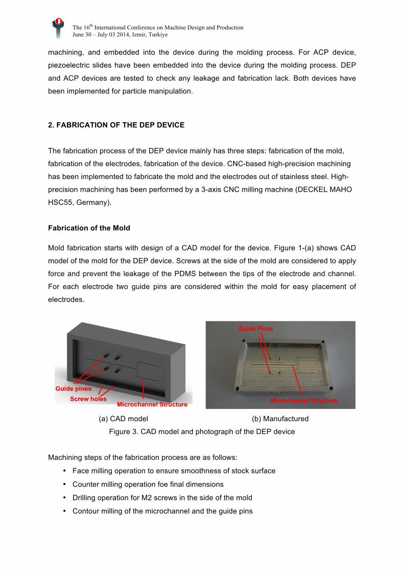
Mold fabrication starts with design of a CAD model for the device. Figure 1-(a) shows CAD
model of the mold for the DEP device. Screws at the side of the mold are considered to apply
force and prevent the leakage of the PDMS between the tips of the electrode and channel.
For each electrode two guide pins are considered within the mold for easy placement of
electrodes.
(a) CAD model (b) Manufactured
Figure 3. CAD model and photograph of the DEP device
Machining steps of the fabrication process are as follows:
• Face milling operation to ensure smoothness of stock surface
• Counter milling operation foe final dimensions
• Drilling operation for M2 screws in the side of the mold
• Contour milling of the microchannel and the guide pins

The 16th International Conference on Machine Design and Production June 30 – July 03 2014, Izmir, Turkiye
Table 1. Machining parameters of the mold of the DEP device
Spindle
Rotational Speed (RPM)
Tool Diameter (mm)
Feed Rate (mm/min)
Depth of Cut (mm)
Rough 12000 2 350 0.1
Semi-Finish 15000 1 150 1
Finish 15000 1 150 1
• Tap milling for M2 screws in the side of the mold
• Pocket milling to open mold cavity
The machining parameters of the mold are tabulated in Table 1. Figure 1-(b) shows
fabricated stainless steel mold. Microchannel has the height of 200µm, width of 100µm and
length of 60 mm. In order to have robust pipe connection in the reservoirs, the depth of the
microchannel cavity has chosen as 3mm. The total machining took approximately 2 hours.
Fabrication of the Electrodes
CNC-based machining has been used to fabricate the electrodes from stainless steel. The
CAD model and manufactured electrodes are shown in Figure 2-(a). Large electrode is 16
mm in length, 1 mm in width and 10 mm in height. The small electrode has the height of 11.5
mm and three tips with width of 500 µm. The space between each tap is 1.5 mm. Two elliptic
guide slots are considered to have easy placement of electrodes in the mold and robust
contact with channel wall. Bottom sides of the electrodes have cavities for the ease of
removal process of the electrodes from the mold during the peel-off, and for a better sealing
at bottom side of the electrodes when the microchannel is bonded to the glass.
(a) CAD model (b) Manufactured
Figure 2. CAD model and photograph of manufactured electrodes

The 16th International Conference on Machine Design and Production June 30 – July 03 2014, Izmir, Turkiye
Table 2. Machining parameters of the electrodes of the DEP device
Spindle
Rotational Speed (RPM)
Tool Diameter (mm)
Feed Rate (mm/min)
Depth of Cut (mm)
Rough 15000 2 850 0.25
Semi-Finish 16000 0.8 150 0.1
Finish 18000 0.6 80 0.1
The steps of the machining process of the electrodes can be summarized as follows:
• Face milling operation to have smooth stock surface
• Pocket milling for cavity and guide slots
• Counter milling for outside of the stock
The machining parameters of the mold are tabulated in Table 2. The fabricated electrodes
are presented in Figure 2-(b). The total machining time for the small and large electrodes
took approximately 30 minutes and 1 hour, respectively.
Fabrication of the Device
Assembly and fabrication process of the DEP device can be summarized as:
• Placement of electrodes in the cavity by aid of guide pins
• Tightening screws in the side wall to prevent the leakage of the PDMS in the interface
of microchannel and electrodes
• Mixing PDMS and curing agent with the ratio of 10:1, and pouring into the mold
• Placing the setup in an oven for PDMS curing (75°C for 45 min)
• Peeling cured PDMS with embedded electrodes from the mold
• Punching out the inlet and outlet reservoirs
• Bonding PDMS to glass slide using plasma bonding

The 16th International Conference on Machine Design and Production June 30 – July 03 2014, Izmir, Turkiye
Figure 3 presents the mold and assembled device used for DEP chip fabrication.
(a) Mold (b) Assembled device
Figure 3. Mold and the assembled DEP device with 3D sidewall electrodes
3. FABRICATION OF THE ACP DEVICE
The fabrication process of the ACP device mainly has two steps: fabrication of the mold and
fabrication of the device. CNC-based high-precision machining has been implemented to
fabricate the mold out of stainless steel. High-precision machining has been performed by a
3-axis CNC milling machine (DECKEL MAHO HSC55, Germany).
Fabrication of the Mold
For ACP device, mold fabrication also starts with designing a CAD model and CNC-based
high precision mechanical machining has been implemented to fabricate the mold out of
stainless steel. Machining steps of the fabrication process are as follows:
• Face milling operation to ensure smoothness of stock surface
• Counter milling operation for final dimensions
• Contour milling of the microchannel and the guide pins
Figure 4 shows fabricated stainless steel mold for ACP device fabrication. In this mold,
microchannel is the height of 130 µm, width of 375 µm and length of 30 mm. The depth of
microchannel cavity as 3mm for the ease and robustness of the fluidic connections on the
reservoirs. The total machining took approximately 2 hours.
Fabrication of the Device
ACP device consists of polymeric channel with piezoelectric (PZT) slides placed in mold
sidewalls. Assembly and fabrication steps for ACP device are summarized as:
• Placement of PZT slides in the cavity
• Mixing PDMS and curing agent with the ratio of 10:1, and pouring into the mold

The 16th International Conference on Machine Design and Production June 30 – July 03 2014, Izmir, Turkiye
Figure 4. Manufactured mold for ACP device
• Placing the setup in an oven for PDMS curing (75°C for 45 min)
• Peeling cured PDMS with embedded PZT slides from the mold
• Punching out the inlet and outlet reservoirs
• Bonding PDMS to glass slide using plasma bonding
Figure 5 shows the mold and assembled device used for ACP chip fabrication.
(a) Mold (b) Assembled device
Figure 5. Mold and the assembled ACP device with embedded PZT slides
Table 3. Machining parameters of the ACT device
Spindle
Rotational Speed (RPM)
Tool Diameter (mm)
Feed Rate (mm/min)
Depth of Cut (mm)
Rough 15000 2 850 0.25
Semi-Finish 16000 0.8 150 0.2
Finish 18000 0.6 80 0.2

The 16th International Conference on Machine Design and Production June 30 – July 03 2014, Izmir, Turkiye
4. RESULTS AND DISCUSSIONS
The fluid is loaded into the fabricated DEP device, and the device is tested for any fluid
leakage (especially around the electrodes), and no leakage has been observed in the device.
Moreover, the device has been examined in details using optical microscopy to find any
PDMS leakage between the channel and electrode interface. It has been observed that there
was direct contact between the electrode and the fluid inside microchannel which is
necessary condition for DEP applications. DEP device has been implemented for n-DEP
particle separation. For the experiment, buffer solution of DI water and 5 µm in diameter
Latex particles has been loaded from inlet reservoir. AC voltage of 5 V and 500 KHz has
been applied to electrodes by using a function generator (Agilent 33250A, Arbitrary
Waveform Generator). Latex particles have been repelled from small electrode due to
negative DEP force (negative DEP is typical for latex particles at this frequency [Cetin,
2011]), and the particles are collected in the outlet reservoir B as expected.
One more advantage of the proposed technique is that the electrodes embedded within the
device are 3D which offers some unique advantages [Cetin and Zeinali, 2014]. Fabrication of
3D sidewall electrodes is not straightforward using lithography-based techniques. Although
some methods have been proposed in the literature [Li, 2014], a fabrication process with
high repeatability, and which enables application of small voltages is still a challenge.
Proposed technique is a promising candidate especially for the microchannels with high
aspect ratio. With the current CNC machining, aspect ratio up to 5 (W: 100 µm, H: 500 µm) is
realizable if needed.
The fabricated ACP device has also been tested and examined to check for any fluid leakage
and fabrication defects within the device, especially in the regions around PZT slides. No
leakage and defects are observed. ACP device has been used successfully for the
manipulation of the 5 µm latex particles towards the channel centerline. It should be also
noted that with the proposed technique, the coupling between the microfluidic device and the
PZT slide seems to be adequate, which is important for the acoustic coupling of the PZT
slide with the microfluidic device. The PZT slides actuated by using a power amplifier
(Electronics & Innovation 1040L Power Amplifier) at 30V and 2MHz. The frequency of the
signal is directly determined by the size of the channel, however the applied voltage is higher
than that of a typical silicon-based ACP device. This is due to the use of PDMS as the device
material. Due to the high voltage and the acoustic heating, some bubble formation is
observed within the microchannels (this issue is also mentioned in the literature [Islam,

The 16th International Conference on Machine Design and Production June 30 – July 03 2014, Izmir, Turkiye
2012]). To overcome this adverse effect some Peltier units based cooling system will be
designed in near future.
Although high precision mechanical machining is implemented for the fabrication of DEP and
ACT based devices, it is not preferable for the hydrodynamic based microfluidic devices [Wu
and Hjort, 2009] in which sharp corners are required for the successful manipulation of
particles within microchannel networks. Some further efforts need to be dedicated to
implement high precision mechanical machining for the fabrication of microchannels with
sharp corners.
5. CONCLUSION
In this study, fabrication procedures for a DEP device and an ACP device for particle
manipulation have been proposed using high precision mechanical machining. Fabrication
process for each device has been described in details, and some preliminary experiments
regarding the particle manipulation have been performed. Although utilizing mechanical
(CNC-based) machining provides limitations for high resolution and complex structures, has
some unique advantages over the lithography-based fabrication such as: manufacturing long
lasting and durable molds, no need for high facility cleanrooms, ease of controllability due to
fewer control parameters and ease of fabrication of high aspect ration channels for high
throughput microfluidic device. This is a pioneer study for the fabrication of microfluidic
devices with embedded 3D electrodes and PZT slides. Following these preliminary
experiments, systematic experiments with latex particles both for DEP and ACP devices
which will be followed by experiments with (bio)particles will be our future research
directions.
ACKNOWLEDGMENT
Financial support from the Turkish Scientific and Technical Research Council, Grant No.
112M102, is greatly appreciated.
REFERENCES
1. Wang, L., Flanagan, LA., Lee, AP., (2007), “Sidewall vertical electrodes for lateral field
microfluidic application”, J Microelectromech S., Vol.16, pp 454-461.
2. Nguyen, NT., Wereley, ST., (2006), Fundamentals and Applications of Microfluidics.
Artech House, pp 49-50, 67-135.

The 16th International Conference on Machine Design and Production June 30 – July 03 2014, Izmir, Turkiye
3. Cetin, B., Li, D., (2011), “Dielectrophoresis in microfluidics technology”, Electrophoresis,
Vol. 32, pp 2410-2427.
4. Islam, AT., Siddique, AH., Ramulu, TS., Reddy, V., Eu, Y-J., Cho, SH., Kim, C.,
(2012), “Ultrasonic alignment of bio-functionalized magnetic beads and live cells in
PDMS micro-fluidic channel”, Biomedical microdevices, Vol. 14 (6), pp 1077-1084
5. Adams, JD., Ebbesen, CL., Barnkob, R., Yang, AHJ., Soh, HT., Bruus, H., (2012),
“High-throughput, temperature-controlled microchannel acoustophoresis device made
with rapid prototyping”, J. Micromech. Microeng., Vol. 22 (7), 075017
6. Cetin, B., Zeinali, S. (2014), “Modeling of on-chip (bio)particle separation and counting
using 3D electrode structures”, Proc. 4th Micro and Nano Flows Conference, UCL,
London, UK, 7-10 September 2014 (accepted)
7. Li, M., Li, W. H., Zhang, J., Alici, G., Wen, W., (2014), “A review of microfabrication
techniques and dielectrophoretic microdevices for particle manipulation and separation”,
J. Physc. D: Appl. Phys., 47, 063001
8. Wu, Z., Hjort, K., (2009), “Microfluidic hydrodynamic cell separation: A review”, Micro
and Nanosystmes, 1 (3), pp 181-192.