Embed Size (px)
Citation preview
FULL P
APER
© 2014 WILEY-VCH Verlag GmbH & Co. KGaA, Weinheim 7085wileyonlinelibrary.com
as a potential material to realize electri-cally pumped organic lasers. Their pos-sible application in fl exible electronics is another motivation for research on the organic single crystals. [ 18,19 ] Organic single crystal-based OLEDs are currently being studied since Pope et al. reported the fi rst OLEDs based on the crystal of anthra-cene. [ 20 ] However, the high-performance OLEDs based on the organic single crystals have been rarely reported. There are sev-eral problems exist which limit the perfor-mance of the organic single crystal-based OLEDs, such as poor charge balance due to the different hole and electron mobility, and diffi culties in the precisely control of both size and thickness of the crystals. The fragility of the organic single crystals leads to a technological challenge in the fabrication of the crystal-based OLEDs with complicated and desired structures,
which is another obstacle to high-performance single crystal-based OLEDs. Effi cient and uniform carrier injection into the crystal is one of the key issues for high effi ciency and long-term stability of the crystal-based OLEDs. However, the fragile crystal was usually laminated onto the bottom electrode and bonded by the weak van der Waals force in the crystal-based OLEDs, [ 9–12 ] which results in a poor contact between the electrodes and crys-tals, and remains the obstacles for the effi cient carrier injection.
In this work, a simple and non-destructive method of tem-plate stripping has been applied to the crystal-based OLEDs to resolve the contact problem. Template stripping technique has been demonstrated to obtain ultrasmooth metallic fi lms for plasmonics and metamaterials, [ 21,22 ] and was employed to realize fl exible OLEDs and organic photovoltaic cells with high fl exibility and effi ciency. [ 23,24 ] On the basis of this technique, both anodes and cathodes of the crystal OLEDs can be directly deposited onto the opposite surface of the organic single crys-tals by thermal evaporation, so that a much improved contact between the crystals and the electrodes can be realized, which enhance the carrier injection into the organic single crystals. The single-crystal-based OLEDs exhibit highly bright and polar-ized EL emission. Moreover, fl exible devices on plastic sub-strate have been obtained, and the devices show superiority in fl exibility and mechanical robustness.
Fabrication and Characterization of Organic Single Crystal-Based Light-Emitting Devices with Improved Contact Between the Metallic Electrodes and Crystal
Ran Ding , Jing Feng , * Xu-Lin Zhang , Wei Zhou , Hong-Hua Fang , Yue-Feng Liu , Qi-Dai Chen , Hai-Yu Wang , and Hong-Bo Sun *
Organic single crystals have attracted great attention because of their advantages of high charge-carrier mobility, high chemical purity, and potential for fl exible optoelectronic devices. However, their intrinsic prop-erties of sensitive to organic solvent and fragile result in a diffi culty in the fabrication of the organic crystal-based devices. In this work, a simple and non-destructive technique of template stripping is employed to fabricate single-crystal-based organic light-emitting devices (OLEDs). Effi cient and uniform carrier injection induced by an improved contact between crystals and both top and bottom electrodes is realized, so that a homogeneous and bright electroluminescence (EL) are obtained. Highly polarized EL and even white emission is also observed. Moreover, the crystal-based OLEDs exhibit good fl exibility, and keep stable EL under a small bending radius and after repeated bending. It is expectable that this technique would support broad applications of the organic single crystals in the crystal-based optoelectronic devices.
DOI: 10.1002/adfm.201400832
R. Ding, Prof. J. Feng, X. L. Zhang, W. Zhou, H. H. Fang, Y. F. Liu, Dr. Q. D. Chen, Prof. H. Y. Wang, Prof. H. B. Sun State Key Laboratory on Integrated Optoelectronics College of Electronic Science and Engineering Jilin University 2699 Qianjin Street , Changchun 130012 , China E-mail: [email protected]; [email protected] Prof. H. B. Sun College of Physics Jilin University 2699 Qianjin Street , Changchun 130023 , China
1. Introduction
Organic single crystals have attracted increasing interests as active material in optoelectronic and electronic devices, for example, organic fi eld-effect transistors (OFETs), [ 1,2 ] light-emitting OFETs, [ 3,4 ] optically pumped lasers, [ 5–8 ] and organic light-emitting devices (OLEDs) [ 9–12 ] because of their advantages such as high order molecular packing, high chemical purity, high charge-carrier mobility, and availability in the low cost and low temperature fabricating process. [ 13–17 ] It is also considered
Adv. Funct. Mater. 2014, 24, 7085–7092
www.afm-journal.dewww.MaterialsViews.com

FULL
PAPER
7086 wileyonlinelibrary.com © 2014 WILEY-VCH Verlag GmbH & Co. KGaA, Weinheim
2. Results and Discussion
2.1. Characteristics of the Organic Single Crystal
Two kinds of organic single crystals, 2,5-bis(4-biphenyl)bith-iophene (BP2T) and 1,4-bis(4-methylstyryl)benzene (BSB-Me) have been employed to fabricate the OLEDs. Figure 1 shows their chemical structure, photographs of thin plate crystal under ultraviolet (UV) light and crystal packing. The crystallographic of data and structure refi nement information is obtained from the Cambridge Structural Database (CSD). The crystals of BP2T and BSB-Me have been demonstrated high luminescence effi -ciencies in the yellow-green and pure-blue emission region, respectively, and excellent amplifi ed spontaneous emission (ASE) characteristics. [ 25,26 ] These two single crystals also have been demonstrated of intense EL emission from the light-emitting OFETs. [ 25,26,40 ] Usually, the crystal-based light-emitting OFETs show a narrow emission zone due to a narrow recom-bination region. While in the case of the crystal-based OLEDs, homogeneous surface emission is possible. In this work, these two typical single crystals are selected to exploit EL emission behavior of the crystal-based OLEDs because of their different directions of transition dipole moments, which would result in a difference in their emission properties. [ 27–29 ] As can been seen in Figures 1 c and d, the photoluminescence (PL) of the BP2T is dominated by edge emission, while both edge and surface PL can be observed from the BSB-Me crystal. This difference is attributed to their different directions of transition dipole moments. As we known, the directions of the transition dipole moments lie along the long axis of the molecule. In the packing of BP2T, the long molecular axis is tiled by 1.2° between the molecular long axis and the normal of the ab -plane. While the molecules of BSB-Me are arranged layer by layer in the herring-bone structure that spread along the ab -plane. [ 2,28 ] Therefore, the transition dipole moments are nearly perpendicular to the crystal plane for the BP2T crystals (Figure 1 e), while in case of the BSB-Me, they are inclined with respect to the crystal plane
(Figure 1 f). Atomic force microscopy (AFM) images of BP2T and BSB-Me single crystals display desirable surface homoge-neity and sharp edges (Figure S1 in Supporting Information).
2.2. Characteristics of the Organic Single Crystal-Based OLEDs
2.2.1. OLEDs Based on Single Crystals of BP2T
Figure 2 shows the schematic of the fabrication process for the crystal-based OLEDs based on the template stripping tech-nique. Octadecyltrichlorosilane (OTS) modifi cation was carried out on the Si/SiO 2 substrate to realize a hydrophobic surface with lowered surface energy, so that the fragile single crystals can be peeled off from the substrate completely during the tem-plate stripping. Au and Ca/Ag are used as anode and cathode. Both anode and cathode were deposited onto the opposite surface of the organic single crystals by thermal evaporation, which ensure a compact contact between the crystal and the electrodes. Based on the technique of template stripping, BP2T-based OLEDs were fi rstly fabricated and characterized. For com-parison, the BP2T-based OLEDs by the laminating method were also fabricated as control and its fabrication schematic is shown in Figure S2. The thickness of the BP2T is around 250 nm. The work function of Au and Ca is 4.7 and 2.87 eV, respectively. The highest-occupied molecular orbital (HOMO) and the lowest unoccupied molecular orbital (LUMO) of BP2T is estimated to be 4.8 eV and 2.8 eV, respectively. [ 25,26 ] Therefore, both anode and cathode possess good energy level matching to ensure an effective hole and electron injection into the organic crystal.
The effect of the improved contact between the electrodes and crystals on the device performance has been verifi ed by comparing the current density-voltage characteristics of the devices fabricated by the template stripping technique and the laminating method. A much higher current density for the template-stripped OLEDs can be seen in Figure 3 , which
Adv. Funct. Mater. 2014, 24, 7085–7092
www.afm-journal.dewww.MaterialsViews.com
Figure 1. Chemical structure of a) BP2T and b) BSB-Me molecules, Fluorescence photograph of c) BP2T and d) BSB-Me crystals under the UV light irradiation, and crystal packing of e) BP2T and f) BSB-Me.

FULL P
APER
7087wileyonlinelibrary.com© 2014 WILEY-VCH Verlag GmbH & Co. KGaA, Weinheim
confi rms an effi cient injection induced by the improved con-tact. Moreover, only edge emission can be obtained for OLEDs based on the laminating method even at a high driving voltage, and nonemissive area and breakage spot can be observed (the inset in Figure 3 ). This is because the rough surface of the
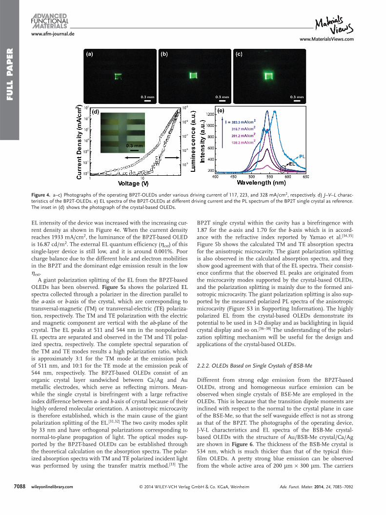
bottom metal electrode results in an incomplete contact when laminating the single crystal onto the bottom electrode. While in the case of the template-stripped OLEDs, homogeneous sur-face emission can be observed at higher current density as can been seen in Figures 4 a–c, which indicates a uniform carrier injection by the improved contact. Therefore the template strip-ping technique employed in the crystal OLEDs has contributed to both effi cient and uniform carrier injection.
The EL from the edge is brighter than that from the surface of the BP2T-based OLEDs as shown in Figures 4 a–c, which can be attributed to the nature of optical confi nement inside the crystal. [ 26,30 ] The direction of transition dipole moments of the BP2T is in pretty good accordance with the molecule long axis. Meanwhile, the molecules are stacked nearly perpendicular to the crystal plane (Figure 1 e), which causes a tendency of the light emission to be parallel to the crystal plane due to the self-waveguide effect. [ 30 ] Figure 4 d shows the current density ( J )–voltage ( V )–luminance ( L ) characteristics of the devices, and the luminance is measured from the normal direction to the device surface. The current density increases at an onset voltage of around 1 V, and an increase in the EL intensity is observed at an onset voltage of around 13 V. The low onset voltage can be ascribed to the improved contact and good energy level matching between the thermal evaporated electrodes and the single crystals, which also results in the homogeneous lumi-nance from the surface as can been seen in Figures 4 a–c. The
Adv. Funct. Mater. 2014, 24, 7085–7092
www.afm-journal.dewww.MaterialsViews.com
Figure 2. Schematic of fabrication process for the crystal-based OLEDs based on the template stripping technique. A single crystal is fi rst transferred onto a Si/SiO 2 substrate (step 1), and a 100 nm thick Au anode is deposited onto the crystal by thermal evaporation (step 2). Then a droplet of pho-topolymer is placed on the crystal (step 3), and the photopolymer is compressed by a fl at glass to form a photopolymer layer at the interface (step 4). After exposed to a UV light source, the cured photopolymer with the Au-coated crystal can be peeled off from the Si/SiO 2 substrate (step 5). And a Ca/Ag cathode is then deposited onto the opposite side of the crystal (step 6). After that the polymer fi lm with the whole crystal-based OLED will be stripped off from the glass (step 7 and 8). Then the fl exible crystal-based OLED is obtained (step 9).
Figure 3. Current density–voltage characteristics of the devices fabricated by the template stripping technique and the laminating method. The inset shows the photograph of the OLEDs fabricated by the laminating method under turn-on (left) and turn-off (right) state.
FULL
PAPER
7088 wileyonlinelibrary.com © 2014 WILEY-VCH Verlag GmbH & Co. KGaA, Weinheim
EL intensity of the device was increased with the increasing cur-rent density as shown in Figure 4 e. When the current density reaches 1933 mA/cm 2 , the luminance of the BP2T-based OLED is 16.87 cd/m 2 . The external EL quantum effi ciency ( η ext ) of this single-layer device is still low, and it is around 0.001%. Poor charge balance due to the different hole and electron mobilities in the BP2T and the dominant edge emission result in the low η ext .
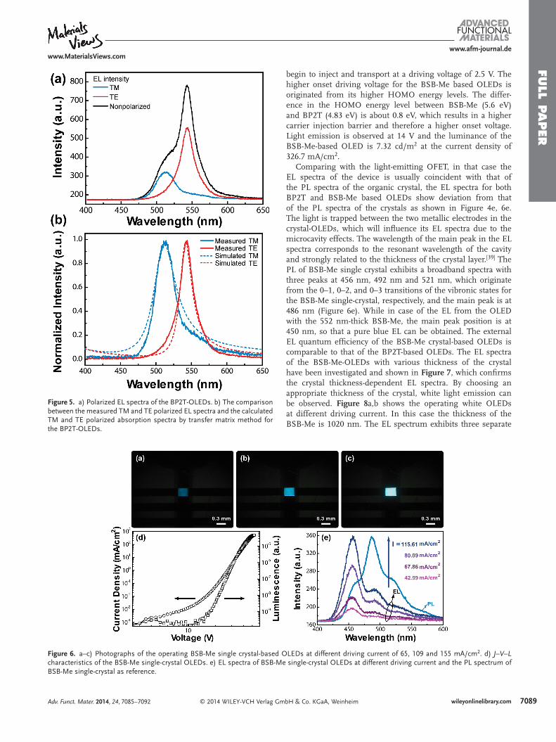
A giant polarization splitting of the EL from the BP2T-based OLEDs has been observed. Figure 5 a shows the polarized EL spectra collected through a polarizer in the direction parallel to the a -axis or b -axis of the crystal, which are corresponding to transversal-magnetic (TM) or transversal-electric (TE) polariza-tion, respectively. The TM and TE polarization with the electric and magnetic component are vertical with the ab -plane of the crystal. The EL peaks at 511 and 544 nm in the nonpolarized EL spectra are separated and observed in the TM and TE polar-ized spectra, respectively. The complete spectral separation of the TM and TE modes results a high polarization ratio, which is approximately 3:1 for the TM mode at the emission peak of 511 nm, and 10:1 for the TE mode at the emission peak of 544 nm, respectively. The BP2T-based OLEDs consist of an organic crystal layer sandwiched between Ca/Ag and Au metallic electrodes, which serve as refl ecting mirrors. Mean-while the single crystal is birefringent with a large refractive index difference between a - and b -axis of crystal because of their highly ordered molecular orientation. A anisotropic microcavity is therefore established, which is the main cause of the giant polarization splitting of the EL. [ 31,32 ] The two cavity modes split by 33 nm and have orthogonal polarizations corresponding to normal-to-plane propagation of light. The optical modes sup-ported by the BP2T-based OLEDs can be established through the theoretical calculation on the absorption spectra. The polar-ized absorption spectra with TM and TE polarized incident light was performed by using the transfer matrix method. [ 33 ] The
BP2T single crystal within the cavity has a birefringence with 1.87 for the a -axis and 1.70 for the b -axis which is in accord-ance with the refractive index reported by Yamao et al. [ 34,35 ] Figure 5 b shows the calculated TM and TE absorption spectra for the anisotropic microcavity. The giant polarization splitting is also observed in the calculated absorption spectra, and they show good agreement with that of the EL spectra. Their consist-ence confi rms that the observed EL peaks are originated from the microcavity modes supported by the crystal-based OLEDs, and the polarization splitting is mainly due to the formed ani-sotropic microcavity. The giant polarization splitting is also sup-ported by the measured polarized PL spectra of the anisotropic microcavity (Figure S3 in Supporting Information). The highly polarized EL from the crystal-based OLEDs demonstrate its potential to be used in 3-D display and as backlighting in liquid crystal display and so on. [ 36–38 ] The understanding of the polari-zation splitting mechanism will be useful for the design and applications of the crystal-based OLEDs.
2.2.2. OLEDs Based on Single Crystals of BSB-Me
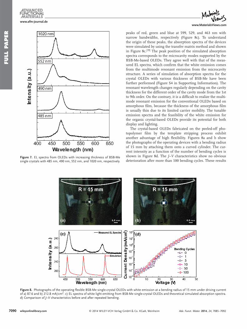
Different from strong edge emission from the BP2T-based OLEDs, strong and homogeneous surface emission can be observed when single crystals of BSE-Me are employed in the OLEDs. This is because that the transition dipole moments are inclined with respect to the normal to the crystal plane in case of the BSE-Me, so that the self waveguide effect is not as strong as that of the BP2T. The photographs of the operating device, J-V-L characteristics and EL spectra of the BSB-Me crystal-based OLEDs with the structure of Au/BSB-Me crystal/Ca/Ag are shown in Figure 6 . The thickness of the BSB-Me crystal is 534 nm, which is much thicker than that of the typical thin-fi lm OLEDs. A pretty strong blue emission can be observed from the whole active area of 200 µm × 300 µm. The carriers
Adv. Funct. Mater. 2014, 24, 7085–7092
www.afm-journal.dewww.MaterialsViews.com
Figure 4. a–c) Photographs of the operating BP2T-OLEDs under various driving current of 117, 223, and 328 mA/cm 2 , respectively. d) J – V – L charac-teristics of the BP2T-OLEDs. e) EL spectra of the BP2T-OLEDs at different driving current and the PL spectrum of the BP2T single crystal as reference. The inset in (d) shows the photograph of the crystal-based OLEDs.
FULL P
APER
7089wileyonlinelibrary.com© 2014 WILEY-VCH Verlag GmbH & Co. KGaA, Weinheim
begin to inject and transport at a driving voltage of 2.5 V. The higher onset driving voltage for the BSB-Me based OLEDs is originated from its higher HOMO energy levels. The differ-ence in the HOMO energy level between BSB-Me (5.6 eV) and BP2T (4.83 eV) is about 0.8 eV, which results in a higher carrier injection barrier and therefore a higher onset voltage. Light emission is observed at 14 V and the luminance of the BSB-Me-based OLED is 7.32 cd/m 2 at the current density of 326.7 mA/cm 2 .
Comparing with the light-emitting OFET, in that case the EL spectra of the device is usually coincident with that of the PL spectra of the organic crystal, the EL spectra for both BP2T and BSB-Me based OLEDs show deviation from that of the PL spectra of the crystals as shown in Figure 4 e, 6 e. The light is trapped between the two metallic electrodes in the crystal-OLEDs, which will infl uence its EL spectra due to the microcavity effects. The wavelength of the main peak in the EL spectra corresponds to the resonant wavelength of the cavity and strongly related to the thickness of the crystal layer. [ 39 ] The PL of BSB-Me single crystal exhibits a broadband spectra with three peaks at 456 nm, 492 nm and 521 nm, which originate from the 0–1, 0–2, and 0–3 transitions of the vibronic states for the BSB-Me single-crystal, respectively, and the main peak is at 486 nm (Figure 6 e). While in case of the EL from the OLED with the 552 nm-thick BSB-Me, the main peak position is at 450 nm, so that a pure blue EL can be obtained. The external EL quantum effi ciency of the BSB-Me crystal-based OLEDs is comparable to that of the BP2T-based OLEDs. The EL spectra of the BSB-Me-OLEDs with various thickness of the crystal have been investigated and shown in Figure 7 , which confi rms the crystal thickness-dependent EL spectra. By choosing an appropriate thickness of the crystal, white light emission can be observed. Figure 8 a,b shows the operating white OLEDs at different driving current. In this case the thickness of the BSB-Me is 1020 nm. The EL spectrum exhibits three separate
Adv. Funct. Mater. 2014, 24, 7085–7092
www.afm-journal.dewww.MaterialsViews.com
Figure 5. a) Polarized EL spectra of the BP2T-OLEDs. b) The comparison between the measured TM and TE polarized EL spectra and the calculated TM and TE polarized absorption spectra by transfer matrix method for the BP2T-OLEDs.
Figure 6. a–c) Photographs of the operating BSB-Me single crystal-based OLEDs at different driving current of 65, 109 and 155 mA/cm 2 . d) J – V – L characteristics of the BSB-Me single-crystal OLEDs. e) EL spectra of BSB-Me single-crystal OLEDs at different driving current and the PL spectrum of BSB-Me single-crystal as reference.
FULL
PAPER
7090 wileyonlinelibrary.com © 2014 WILEY-VCH Verlag GmbH & Co. KGaA, Weinheim
peaks of red, green and blue at 599, 529, and 463 nm with narrow bandwidths, respectively (Figure 8 c). To understand the origin of these peaks, the absorption spectra of the devices were simulated by using the transfer matrix method and shown in Figure 8 c. [ 39 ] The peak position of the simulated absorption spectra corresponds to the microcavity modes supported by the BSB-Me-based OLEDs. They agree well with that of the meas-ured EL spectra, which confi rm that the white emission comes from the multimode resonant emission from the microcavity structure. A series of simulation of absorption spectra for the crystal OLEDs with various thickness of BSB-Me have been further performed (Figure S4 in Supporting Information). The resonant wavelength changes regularly depending on the cavity thickness for the different order of the cavity mode from the 1st to 9th order. On the contrary, it is a diffi cult to realize the multi-mode resonant emission for the conventional OLEDs based on amorphous fi lm, because the thickness of the amorphous fi lm is usually thin due to its limited carrier mobility. The tunable emission spectra and the feasibility of the white emission for the organic crystal-based OLEDs provide its potential for both display and lighting.
The crystal-based OLEDs fabricated on the peeled-off pho-topolymer fi lm by the template stripping process exhibit another advantage of high fl exibility. Figures 8 a and b show the photographs of the operating devices with a bending radius of 15 mm by attaching them onto a curved cylinder. The cur-rent intensity as a function of the number of bending cycles is shown in Figure 8 d. The J – V characteristics show no obvious deterioration after more than 100 bending cycles. These results
Adv. Funct. Mater. 2014, 24, 7085–7092
www.afm-journal.dewww.MaterialsViews.com
Figure 7. EL spectra from OLEDs with increasing thickness of BSB-Me single crystals with 485 nm, 490 nm, 552 nm, and 1020 nm, respectively.
Figure 8. Photographs of the operating fl exible BSB-Me single-crystal OLEDs with white emission at a bending radius of 15 mm under driving current of a) 87.6 and b) 212.8 mA/cm 2 . c) EL spectra of white light emitting from BSB-Me single-crystal OLEDs and theoretical simulated absorption spectra. d) Comparison of J – V characteristics before and after repeated bending.

FULL P
APER
7091wileyonlinelibrary.com© 2014 WILEY-VCH Verlag GmbH & Co. KGaA, WeinheimAdv. Funct. Mater. 2014, 24, 7085–7092
www.afm-journal.dewww.MaterialsViews.com
demonstrate that single-crystal OLEDs are not only highly fl ex-ible but also mechanically robust.
3. Conclusion
In summary, a simple and non-destructive method of tem-plate stripping has been applied to the organic single crystal-based OLEDs to improve the contact between the electrode and crystal. Both surface and edge emission have been realized by using two kinds of crystals. Highly polarized EL and white emission are also observed from the crystal-based OLEDs. Not only bright and homogeneous luminescence but also high fl ex-ibility and mechanical robustness have been realized. These results indicate a universality of the template stripping tech-nique in fabricating the crystal-based optoelectronic devices, which provides an avenue to promote their broad applications.
4. Experimental Section Crystal Growth : BP2T and BSB-Me powders were purchased from
Lumtec Corp. and Tokyo Chemical Industry Co. Ltd., respectively. The single crystals were grown by horizontal physical vapor transport in a rapid crystal growth condition. Very thin, large, and fl at crystals were obtained on the inner glass cylinders with sublimation temperatures of 380 °C and 270 °C. High-purity argon was adopted as carrier and to prevent the organic materials from being oxidized. The gas fl owing rates were varied between 10 and 50 mL min −1 , with an optimal fl ow of 40 mL min −1 . [ 41,42 ] Under the optimal fl ow, the thin crystal materials can be grown as thin as 200–300 nm and as large as 3 mm × 3 mm in size by rapid growth conditions. Either higher or lower fl ow rates will result in non-crystalline or thicker crystals.
Device Fabrication : Octadecyltrichlorosilane (OTS) modifi cation was carried out on the cleaned SiO 2 /Si substrates for about 4 h by vapor-deposition method to realize a hydrophobic surface of low-surface-energy. Then the substrates were rinsed with chloroform, alcohol, deionized water by ultrasonic cleaning and dried with quick purged N 2 . After that, single crystal was transferred onto this pre-modifi ed Si/SiO 2 substrate with the hydrophobic surface. Then a 100 nm thick Au anode was deposited onto the organic crystal by thermal evaporation. A droplet of photopolymer (NOA63, Norland) was placed at around the center of the Au coated crystal surface. After the droplet was compressed by a piece of glass with 0.6-mm thickness, a photopolymer layer was formed on the Au/crystal coated highly hydrophobic substrate by capillarity forces. The photopolymer spread across the whole hydrophobic surface and fi lled up the empty space between the polymer and the glass. The glass-photopolymer-Au/crystal-silicon sandwich structure was pressed with the whole weight of the glass itself and thickness of the photopolymer fi lms ranged between 0.3–0.8 mm. Then the sandwich structure was exposed to a UV light source at power of 125 W for 10 min. The cured photopolymer with the Au/crystal can be peeled off, due to the better adhesion between the Au/crystal and photopolymer compared with that between the crystal and the OTS-treated Si/SiO 2 substrate. Also it was generally attributed to the differences in the surface energy of the substrates and the crystals (Figure S5 in Supporting Information). A 10 nm Ca and 30 nm Ag cathode was evaporated onto the template-stripped organic crystal. At last a fl exible organic crystal-based OLED was obtained by peeled off the photopolymer from the glass. The electrodes were deposited by thermal evaporation in high vacuum system at a rate of 1 Å/s at a base pressure of 5 × 10 −4 Pa. The active area of the device was determined by mask of metal temple of 200 µm × 300 µm.
Characterizations : The J – V – L characteristics of the devices were measured by a Keithley 2400 programmable voltage-current source and photomultiplier tube. And the brightness of the crystal-based OLEDs
was detected by the Photo Research PR-655 spectrophotometer. The photographs of crystals were taken by using widefi eld fl uorescence microscopy on BK-FL4 fl uorescence microscope. The emission spectra were detected by the optical fi ber and then dispersed to the spectrometer connected with charge coupled device detector. The contact angle (CA) was measured using a Contact Angle System OCA 20 instrument (DataPhysics Instruments GmbH, Germany) with a high purity water droplet (≈5 mL) deposited on the sample surface. The fi lm thicknesses for single crystals were measured by AFM (Digital Instruments Nanoscope ?A) in the tapping mode. All of the measurements were conducted in air at room temperature.
Numerical Simulation : The transfer matrix method is applied to calculate the absorption spectra of the crystal OLEDs. The relative permittivity and permeability of the anisotropic active layer can be described as:
εε
εε
μ=
⎡
⎣
⎢⎢⎢⎢
⎤
⎦
⎥⎥⎥⎥
=⎡
⎣
⎢⎢⎢
⎤
⎦
⎥⎥⎥
0 0
0 0
0 0
1 0 0
0 1 0
0 0 1a a
x
Y
z
where z corresponds to the layer direction. Taking TM-polarized case with electromagnetic components of E x , E z , and H y for instance, we assume an incidence coming from a media with refractive index of n. The magnetic fi eld in the anisotropic active layer can then be described as ( ) ( )= Λ + −ΛH A z B zy exp expa
a a a a , where A a and B a are undetermined amplitude coeffi cients, and
ε εΛ = −⎛⎝⎜
⎞⎠⎟
jkn
xz
1a 0
2. For electromagnetic waves in the isotropic layer
with a relative permittivity of ε i , the magnetic fi eld can be described as
( ) ( )= Λ + −ΛH A z B zy exp expii i i i , where εΛ = −jk ni 0 i
2 . By applying
the relationship of ε= − ∂∂E
jk
Hzx
x
ya
0
a
for waves in the anisotropic active
layer and ε= − ∂∂E
jk
Hzx
yi
0 i
i
for waves in the isotropic layer, respectively,
the x -direction electric fi eld can also be written. Then the undetermined amplitude coeffi cients A a , B a , A i , and B i can be solved by applying the continuity of the tangential electromagnetic components ( E x and H y ) in the layer boundary to obtain the transfer matrix between each adjacent layer. Once the amplitude coeffi cients are obtained, the absorption spectra can be calculated by some further operations of the Poynting vectors.
Supporting Information Supporting Information is available from the Wiley Online Library or from the author.
Acknowledgements The authors gratefully acknowledge the fi nancial support from the 973 Project (No. 2013CBA01700) and NSFC Grants (Nos. 61322402, 91233123, 51373064 and 61177024).
Received: March 13, 2014 Revised: July 28, 2014
Published online: September 10, 2014
[1] T. Katagiri , Y. Shimizu , K. Terasaki , T. Yamao , S. Hotta , Org. Electron. 2011 , 12 , 8 .
[2] H. Nakanotani , M. Saito , H. Nakamura , C. Adachi , Appl. Phys. Lett. 2009 , 95 , 033308 .

FULL
PAPER
7092 wileyonlinelibrary.com © 2014 WILEY-VCH Verlag GmbH & Co. KGaA, Weinheim Adv. Funct. Mater. 2014, 24, 7085–7092
www.afm-journal.dewww.MaterialsViews.com
[3] H. Nakanotani , M. Saito , H. Nakamura , C. Adachi , Appl. Phys. Lett. 2009 , 95 , 103307 .
[4] H. Wang , F. Li , I. Ravia , B. Gao , Y. Li , V. Medvedev , H. Sun , N. Tessler , Y. Ma , Adv. Funct. Mater. 2011 , 21 , 3770 .
[5] T. Hiramatsu , N. Matsuoka , H. Yanagi , F. Sasaki , S. Hotta , Phys. Status. Solidi. C 2009 , 6 , 338 .
[6] R. Ding , H. H. Fang , Y. Wang , S. Y. Lu , X. L. Zhang , L. Wang , J. Feng , Q. D. Chen , H. B. Sun , Org. Electron. 2012 , 13 , 1602 .
[7] H. H. Fang , Q. D. Chen , J. Yang , H. Xia , B. R. Gao , J. Feng , Y. G. Ma , H. B. Sun , J. Phys. Chem. C 2010 , 114 , 11958 .
[8] Q. D. Chen , H. H. Fang , B. Xu , J. Yang , H. Xia , F. P. Chen , W. J. Tian , H. B. Sun , Appl. Phys. Lett. 2009 , 94 , 201113 .
[9] M. Ichikawa , K. Nakamura , M. Inoue , H. Mishima , T. Haritani , R. Hibino , T. Koyama , Y. Taniguchi , Appl. Phys. Lett. 2005 , 87 , 221113 .
[10] X. Li , Y. Xu , F. Li , Y. Ma , Org. Electron. 2012 , 13 , 762 . [11] H. Nakanotani , C. Adachi , Appl. Phys. Lett. 2010 , 96 , 053301 . [12] H. Yanagi , T. Morikawa , S. Hotta , Appl. Phys. Lett. 2002 , 81 , 1512 . [13] H. Nakanotani , M. Saito , H. Nakamura , C. Adachi , Adv. Funct.
Mater. 2010 , 20 , 1610 . [14] R. Kabe , H. Nakanotani , T. Sakanoue , M. Yahiro , C. Adachi , Adv.
Mater. 2009 , 21 , 4034 . [15] K. Kajiwara , K. Terasaki , T. Yamao , S. Hotta , Adv. Funct. Mater. 2011 ,
21 , 2854 . [16] K. Sawabe , M. Imakawa , M. Nakano , T. Yamao , S. Hotta , Y. Iwasa ,
T. Takenobu , Adv. Mater. 2012 , 24 , 6141 . [17] S. Hotta , T. Yamao , S. Z. Bisri , T. Takenobu , Y. Iwasa , J. Mater.
Chem. C 2014 , 2 , 965 . [18] A. L. Briseno , S. C. B. Mannsfeld , M. M. Ling , S. H. Liu , R. J. Tseng ,
C. Reese , M. E. Roberts , Y. Yang , F. Wudl , Z. N. Bao , Nature 2006 , 444 , 913 .
[19] A. L. Briseno , R. J. Tseng , M. M. Ling , E. H. L. Falcao , Y. Yang , F. Wudl , Z. Bao , Adv. Mater. 2006 , 18 , 2320 .
[20] M. Pope , H. P. Kallmann , P. Magnante , J. Chem. Phys. 1963 , 38 , 2042 .
[21] P. Nagpal , N. C. Lindquist , S.-H. Oh , D. J. Norris , Science 2009 , 325 , 594 .
[22] N. C. Lindquist , T. W. Johnson , D. J. Norris , S.-H. Oh , Nano Lett. 2011 , 11 , 3526 .
[23] Y. F. Liu , J. Feng , D. Yin , Y. G. Bi , J. F. Song , Q. D. Chen , H. B. Sun , Opt. Lett. 2012 , 37 , 1796 .
[24] Y. F. Liu , J. Feng , H. F. Cui , D. Yin , J. F. Song , Q. D. Chen , H. B. Sun , Appl. Phys. Lett. 2012 , 101 , 133303 .
[25] H. Nakanotani , R. Kabe , M. Yahiro , T. Takenobu , Y. Iwasa , C. Adachi , Appl. Phys. Express. 2008 , 1 , 091801 .
[26] Y. Wang , R. Kumashiro , Z. Li , R. Nouchi , K. Tanigaki , Appl. Phys. Lett. 2009 , 95 , 103306 .
[27] T. Sengoku , T. Yamao , S. Hotta , J. Non-Cryst. Solids. 2012 , 17 , 2525 . [28] S. Hotta , M. Goto , R. Azumi , M. Inoue , M. Ichikawa , Y. Taniguchi ,
Chem. Mater. 2004 , 16 , 237 . [29] H. H. Fang , Q. D. Chen , J. Yang , H. Xia , Y. G. Ma , H. Y. Wang ,
H. B. Sun , Opt. Lett. 2010 , 35 , 441 . [30] S. Z. Bisri , T. Takenobu , Y. Yomogida , H. Shimotani , T. Yamao ,
S. Hotta , Y. Iwasa , Adv. Funct. Mater. 2009 , 19 , 1728 . [31] T. Virgili , D. G. Lidzey , M. Grell , S. Walker , A. Asimakis ,
D. D. C. Bradley , Chem. Phys. Lett. 2001 , 341 , 219 . [32] M. Theander , T. Granlund , M. D. Johanson , A. Ruseckas ,
V. Sundstrom , M. R. Andersson , O. Ingänas , Adv. Mater. 2001 , 13 , 323 . [33] P. Yeh , Optical waves in layered media , Wiley , New York 1988 . [34] T. Yamao , N. Sakamoto , S. Hotta , H. Mizuno , H. Yanagi , Jpn. J.
Appl. Phys. 2012 , 51 , 11PD03 . [35] T. Yamao , Y. Okuda , Y. Makino , S. Hotta , J. Appl. Phys. 2011 , 110 ,
053113 . [36] S. Stelitano , G. De Luca , S. Savasta , S. Patané , Appl. Phys. Lett.
2008 , 9 3 , 193302 . [37] S. Stelitano , S. Savasta , S. Patané , G. De Luca , L. Monsù Scolaro , J.
Appl. Phys. 2009 , 106 , 033102 . [38] E. Matioli , S. Brinkley , K. M. Kelchner , Y.-L. Hu , S. Nakamura ,
S. DenBaars , J. Speck , C. Weisbuch , Light Sci. Appl. 2012 , 1 , e22 . [39] H. Zhang , H. You , W. Wang , J. Shi , S. Guo , M. Liu , D. Ma , Semi-
cond. Sci. Tech. 2006 , 21 , 1094 . [40] K. Oniwa , T. Kanagasekaran , T. Jin , M. Akhtaruzzaman ,
Y. Yamamoto , H. Tamura , I. Hamada , H. Shimotani , N. Asao , S. Ikeda , K. Tanigaki , J. Mater. Chem. C 2013 , 1 , 4163 .
[41] R. A. Laudise , C. Kloc , P. G. Simpkins , T. Siegrist , J. Crystal Growth 1998 , 187 , 449 .
[42] L. B. Roberson , J. Kowalik , L. M. Tolbert , C. Kloc , R. Zeis , X. Chi , R. Fleming , C. Wilkins , J. Am Chem Soc. 2005 , 127 , 3069 .