Embed Size (px)
Citation preview

Master of Science ThesisStockholm, Sweden 2013
TRITA-ICT-EX-2013:238
M E L K A M U B E L E T E
Fabrication and Characterization ofTunneling Oxides on Graphene
K T H I n f o r m a t i o n a n d
C o m m u n i c a t i o n T e c h n o l o g y

Fabrication and Characterization of Tunneling
Oxides on Graphene
Melkamu Belete
Master’s Thesis Submitted as a Partial Fulfillment for MSc Degree in Nanotechnology
Department of
Integrated Devices and Circuits (IDC) The Royal Institute of Technology (KTH)
Stockholm, Sweden. Sept. 2013
Supervisor:
Prof. Dr. Eng. Max Lemme
Examiner: Prof. Mikael Östling
Practical Coach and Supervisor:
Sam Vaziri

i

ii
Abstract
Graphene base transistors (GBTs) are known to be novel devices mingling outstanding properties
of graphene, with the concept of hot electron transistors (HETs). According to theoretical
calculations, GBTs were predicted to have over 5 orders of magnitude ON/OFF current ratios and
THz frequency range operations. This would in fact lead to potential applications in high speed
radio frequency (RF) analog devices. Recently, GBTs’ high gain and more than 4 orders of
magnitude ON/OFF current ratios have been experimentally proven. However, GBTs still need
further improvements before they can be applied in real electronics devices; and that can be done
through thickness and barrier height optimization of the tunneling barrier.
In this thesis project, we have studied various gate dielectrics for potential applications as
tunneling barriers in GBTs. To accomplish this study, we have gone through two rounds of
successful cleanroom fabrication processes, where we fabricated fully functional devices. During
the first round, we have developed seven different capacitor structures on 4 inch Si wafers with
ALD deposited: Al2O3, TiO2, HfO2, “Al2O3+TiO2 mix”, SiO2/HfO2 stack, SiO2/Al2O3 stack and
thermally grown SiO2 dielectrics. Whereas in the second batch, BG-GFET structures were
fabricated on chip level, with: 2nm SiO2, 5nm SiO2, 10nm SiO2, (2nm/4.2nm) SiO2/HfO2,
(2nm/4.5nm) SiO2/”Al2O3+TiO2 mix”, 6nm “Al2O3+TiO2 mix” and 6.6nm TiO2 bottom gates,
onto which a single layer graphene was transferred. We have also carried out electrical
characterizations of these successfully fabricated devices and making use the encouraging results
obtained, we have investigated the associated current injection mechanisms across each barrier.

iii
Acknowledgements
Before any one and anything, I wanna thank the Almighty for being my courage and strength to
do what I did, and also for blessing me with the wisdom that enabled me see the light far beyond
the shadow of darkness. The belief and faith I had in Him had been my genuine bravery and
absolute drive that carried me all the way through. I am also very much indebted to my wonderful
family- my foundation and I wanna congratulate them that the seed they sow is still blossoming!
From deep my heart, I would like thank my supervisor Prof. Dr.-Eng. Max Lemme for all his wise
guidances, rewarding discussions and caring advices. He is a gifted teacher, a great supervisor and
a considerate and amazing human being. His best qualities have been the fundamental drives
behind my ambitious start and successful achievements of this thesis project. And I would remain
indebted to all he has done to me; if it was not for him, today would not have been a reality!
I would like to thank my examiner Prof. Mikael Östling for valuable discussions, useful advices
and honest comments. Every time I needed, his door has always been open for me for discussions.
He has fulfilled all the necessary facilities for my work and encouraged me throughout the
process. He has been far more than an examiner for me and I am very much grateful for all that.
My heartfelt thanks shall go out to Sam Vaziri for his determination in teaching me all the
practical aspects and also for his devotion and tireless supervision of my work throughout this
project. He has always been very positive and very friendly; and also he always finds time for me
even being in the midst of very tight situations. I would not ask a better person to work with.
I would like to thank Anderson Smith for his support and kind help during fabrication and also for
fruitful discussions. I would like to send out my thanks to Prof. Per. Erik Helström for a very
useful discussion on CV data and CV measurement. I am also grateful to Prof. Gunar Malm for
his help during characterization. I would like to thank Eugenio Dentoni Litta for great discussions
on CV. Maziar Manouchehry, Sreejith Ganesh and all other friends who, in one way or another,
have helped me out during my project work deserve my heartfelt thanks for their helps and
supports. I also would like to deliver my very special thanks to my dear friends Seyoume Tsige,
Ansha Hamid, Endalkachew Melkamu and Wondwossen Bekele for their amazing supports and
encouragements during my studies.

iv
Last but not least, I would like to mention my deepest love and gratitude to my beloved best
friend in the whole universe, my precious gift from the Almighty, the courage of my journey, the
queen of my heart and the love of my life- Haimanot. Haimye, words are not good enough to
describe what you really mean to me nor do they express what you really have done to me. Hence,
I shall end saying this: thanks for reminding me of my mom in every way, through who you are!

v
TABLE OF CONTENTS
Abstracts …………………………………………………………………………………………………………………… i
Acknowledgements …………………………………………………………………………………………………… ii
1. INTRODUCTION ......................................................................................................................................... 1
2. BACKGROUNDS .......................................................................................................................................... 3
2.1. GRAPHENE ..................................................................................................................................................... 3
2.1.1. Properties of Graphene......................................................................................................................... 3
2.1.2. Applications of Graphene...................................................................................................................... 5
2.1.3. Techniques of Graphene Production ................................................................................................... 6
2.2. GRAPHENE-BASE TRANSISTORS (GBTS) ..................................................................................................... 7
2.2.1. Basic structure of a GBT ....................................................................................................................... 7
2.2.2. Operation/Working Principles of GBTs ................................................................................................ 8
2.2.3. Applications of GBTs ............................................................................................................................ 9
2.2.4. Main advantages of GBTs over ordinary HETs .................................................................................... 9
2.3. BASIC PRINCIPLES OF QUANTUM TUNNELING ............................................................................................. 10
2.4. CURRENT INJECTION MECHANISMS ACROSS THIN BARRIERS ................................................................................ 12
2.4.1. Direct Tunneling (DT) ........................................................................................................................ 12
2.4.2. Fowler-Nordheim Tunneling (FNT) .................................................................................................... 13
2.4.3. Thermionic/ Schottky Emission (SE) ................................................................................................... 15
2.4.4. Defect Mediated Tunneling (DMT) ..................................................................................................... 16
3. DEVICE FABRICATION ........................................................................................................................... 20
3.1. FABRICATION OF MOS CAPACITOR STRUCTURES .................................................................................... 20
3.1.1. Substrate preparation .......................................................................................................................... 20
3.1.2. Thin dielectric layer formation ........................................................................................................... 20
3.1.3. Top and back contact formations ........................................................................................................ 22
3.1.4. Patterning/Photolithography .............................................................................................................. 23
3.1.5. Summary.............................................................................................................................................. 23
3.2. FABRICATION OF (BG-GFET) STRUCTURES ............................................................................................. 24
3.2.1. Substrate description and preparation ................................................................................................ 25
3.2.2. Thin High-k dielectric deposition ........................................................................................................ 25
3.2.3. Graphene Transfer .............................................................................................................................. 26
3.2.4. Patterning / Photo-Lithography .......................................................................................................... 27
3.2.5. Back and Top-Contact Formations ..................................................................................................... 29
3.2.6. Summary.............................................................................................................................................. 29
4. CHARACTERIZATION ............................................................................................................................. 33

vi
4.1. ELLIPSOMETRY .............................................................................................................................................. 33
4.2. RAMAN SPECTROSCOPY .................................................................................................................................. 34
4.3. ELECTRICAL MEASUREMENTS AND MEASUREMENT SETUPS ............................................................................. 34
4.3.1. CV and IV measurements on MOS Capacitors ................................................................................... 35
4.3.2. IV and Temperature dependent-IV measurements on BG-GFETs ..................................................... 36
5. PRESENTATION AND DISCUSSION OF RESULTS .............................................................................. 37
5.1. CV- CHARACTERISTICS OF THE MOS CAPACITORS .......................................................................................... 37
5.2. IV- CHARACTERISTICS OF THE MOS CAPACITORS ........................................................................................... 39
5.3. IV-CHARACTERISTICS OF THE BG-GFETS ...................................................................................................... 41
5.3.1. Transfer characteristics ...................................................................................................................... 41
5.3.2. Leakage Characteristics ...................................................................................................................... 43
5.3.3. Analysis of Tunneling Currents for investigation of transfer mechanisms .......................................... 45
6. CONCLUSIONS AND OUTLOOKS .......................................................................................................... 60
7. REFERENCES ............................................................................................................................................ 62

1
1. Introduction
It is an absolute reality that technology assists and simplifies the day-to-day activities of human
beings all around the world, from every walk of life. And electronics technology is the drive for
advancement that has made tremendous contributions to the modern world we see today.
Electronics devices are made up of major components known as “integrated circuits (ICs)”, which
in turn are comprised of large number of transistors. In producing faster, smaller and cheaper ICs,
industries have managed to fulfill “Moore’s Law” for almost five decades, successively
downscaling the CMOS transistors. However, further downscaling is not possible any more due to
the physical limitations of materials in CMOS transistors. Hence, to maintain advancement in
electronics, a massive research has been devoted to establish outstanding designs and find
alternative materials with much better electrical properties and higher tendency for downscaling
beyond the limits of silicon. Fortunately, there comes the discovery of a one atom-thick 2D
graphene, with outstanding electrical properties suitable for future small and efficient electronics.
2004 will definitely go down in history as the year in which A.Geim and K.Novoselov gave birth
to graphene [1], which in fact was conceived by P.R.Wallace more than half a century ago [2].
Since its experimental birth, graphene has stayed a hot issue which the research world’s attention
has been pivoted on, and so is today. Graphene’s amazing mechanical and electrical properties
such as: it’s strength and extreme thinness, as well as the ultrahigh intrinsic mobility of its
massless fermions [3], gave bright hope for researchers to replace the channel material in
conventional field effect transistors (FETs). As a result, graphene field effect transistors (GFETs)
[4], which were hoped to substitute conventional MOSFETs, were built. Nevertheless, it wasn’t
too long before GFET’s “logic” application became challenging due to their low “ON/OFF”-
current ratio, which in fact resulted from the absence of band-gap in graphene [5]. The extensive
research continued towards taking advantage of graphene’s super properties for transistor
applications. In return, the first graphene-base transistor (GBT) was introduced in 2012, and that
has laid the foundation for RF and high speed electronics applications of graphene transistors [6].
The main target of this thesis project has been finding optimized tunneling barriers, through
investigation of current transfer properties across different dielectric materials that could be
potential candidates, to enhance the performance of GBTs. To furnish the reader with the

2
necessary background informations: complete story of graphene, brief descriptions of graphene-
base transistors (GBTs), as well as basic principles and types of quantum tunneling are covered in
chapter two.
The project in general involved two batches of complete device fabrication processes, which lead
to successful demonstrations of working devices. During the first batch, seven types of MOS
capacitor structures were fabricated to study seven different dielectric materials. Based on the first
batch results, bottom-gate graphene field effect transistors (BG-GFETs) were fabricated, through
which the current transfer properties across the tunneling barriers were investigated. Details of the
fabrication processes of these two batches of devices are extensively reported in chapter three.
Devices obtained from the successful fabrication processes were then measured and attested to be
fully functional, through electrical characterization. Capacitance-voltage (CV), current-voltage
(IV) and temperature-dependent current-voltage (temp.-dep. IV) measurements have been
extensively made and large amount of data were retrieved. Measurement setups and details of the
characterization processes in general can be found in chapter four, where it is briefly described
and illustrated. The electrical measurement data were then processed and analyzed by making use
of the so called “Origin lab” data processing computer program, and the final results are
exclusively discussed in chapter five. Finally, based on the results achieved, reasonable
conclusions are drawn and fruitful suggestions for future work are highlighted in chapter six.

3
2. Backgrounds
2.1. Graphene
Originated from the natural 3D graphite, graphene is well known as a two-dimensional and single
atomic layer, crystalline material. Its structure merely comprises of sp2-bonded carbon atoms
(Figure 2.1b), whose configuration resulted in the honey comb crystal structure [7]. It is a bare
truth that, the idea of graphene was first introduced to the world more than half a century ago, by
P.R.Wallace [2]. Nevertheless, almost six decades were counted before it was experimentally
realized in 2004, by the Manchester university’s A.Geim and K.Novoselov [1], for which they
earned a Nobel-prize in 2010. After this experimental discovery, graphene has become one of the
hot issues that have conquered the world, ever.
The upcoming sub-sections will exhaustively deal with properties and applications of graphene,
which results from its peculiar dimensionality and unique nature. The techniques commonly used
to produce graphene will be covered too.
2.1.1. Properties of Graphene
The honey-comb structure of graphene is established in such a way that, two atoms are
accommodated in each unit cell of a hexagonal lattice. This hexagonal lattice can in general be
regarded as, two equivalent triangular sub-lattices A and B with inversion symmetry (figure 2.1
a). Each carbon atom in the trigonal planar structure of graphene, contributes sp2 hybrids to form
“σ-bonds” with three others [8]. The mechanical properties of graphene are attributed to these σ-
bonds, which are strong carbon-carbon bonds, making graphene the strongest material [7], [9].
Following this, graphene is termed as thermally stable and chemically inert [7]. On the other hand,
carbon atoms of the unhybridized P-orbitals, which are normal to the planar structure, bind to
adjacent carbon atoms and result in a partially-filled “π-bond”. This “π-bond” in turn gives rise to
the energy band structure of graphene illustrated in (figure 2.2b&c) and has fully taken the credit
for the unique and outstanding electronic properties of graphene.

4
From the energy band structure of graphene shown in figure 2.2b, one can observe that, the
vertices of the conduction and valence bands meet at the corners of the hexagonal brillouin zone,
which lie at zero energy K-points of the reciprocal lattice. These k-points are called Dirac points,
in the locality of which charge carriers attain a linear dispersion relation, which can solely be
ruled by Dirac equation instead of Schrödinger’s [5]. It is strongly believed that, carriers in
graphene can easily and freely traverse between the bands; and that is why graphene is regarded
as a semi-metal, or a semiconductor with no band gap (figure 2.2c) [5].
Equation (2.1) bellow signifies the low energy dispersion relations of graphene near its Dirac
points, employing the idea of zero effective mass for holes and electrons moving with a constant
Fermi velocity:
Figure 2.2:- a) First Brillouin zone of graphene lattice b) Electronic dispersion of graphene. The π-band (red) and the π*-band (blue) touch each other at singularity points (K and K' points) and (c) Zoomed-view of the canonical form dispersion at the singularity points, with an approximately linear slope [75]
(b) (a)
Figure 2.1:-(a) Graphene lattice structure with two equivalent triangular sub lattices in red and blue: δi, i=1,2,3 are the three closest neighbor bonds and a1 and a2 are the basis vectors [Online] ; (b) Schematics of the σ-and π- orbitals of one carbon atom in graphene [4]

5
√
Eqn (2.1)
Where, is the Fermi velocity of electrons and holes in graphene [2].
On the basis of the linear dispersion relations in graphene, its carriers at low energy are termed as
massless Dirac fermions, which are mainly characterized by their speed of propagation, just like
phonons [10], [11].
Charge carriers in graphene sheet have a submicron length range mean free path, within which
they undergo ballistic transport [5], [12], [13]. And that resulted in graphene’s high carrier
mobilities: 15000 cm2
V-1
s-1
for graphene on SiO2 substrate [10], 27000 cm2
V-1
s-1
for epitaxial
graphene [14] and even > 200000 cm2
V-1
s-1
for suspended graphene [3][15]. Hence, graphene’s
mobility is found to be far better than that of conventional silicon. Nonetheless, mobility of
graphene in real electronics devices is expected to be affected by scattering due impurity centers
[16]. In addition to mobility, many other remarkable properties of graphene are also highlighted
by many experimental results including: extremely high thermal conductivity at room temperature
[17], High transparency [18], and high mechanical stability [19].
2.1.2. Applications of Graphene
All special properties and remarkable features described in the above sub-section have made
graphene an excellent material with immense potentials and promising applications, in quiet many
horizons of science and technology. It in short is considered as a material with a huge potential to
revolutionize technology, and as a result has become a common language for almost all engineers
and scientists around the globe. In electronics, graphene can be used as a channel material for
graphene field effect transistors (GFETs) [20] as well as a base for graphene-base transistors
(GBTs) [6], which are believed to be alternatives for “post-silicon-electronics” [21].
As a matter of fact, the absence of band-gap in graphene’s natural state has resulted in a very low
on-off-current ratio in GFETs, which hindered graphene’s journey of taking over silicon’s place in
digital logic applications. However, researchers have claimed that, ON-OFF ratio can be
improved by inducing a band-gap to graphene’s structure, for example: by cutting graphene sheet
in to nanoribbons [22], [23], Sandwiching graphene film in between two hexagonal boron nitride

6
layers [24], and inducing asymmetry to the AB-stacked graphene bilayers by applying a strong
perpendicular electric field [20]. On the other hand, there are areas where, graphene’s lack of
band-gap is not a setback. For instance, graphene can be used in radio-frequency analog
transistors and ultrafast photodetectors [20], for frequency amplifiers [25] and for RF-mixers [26].
In addition, graphene’s high thermal conductivity and its ability of holding large current density
has made it a suitable candidate for interconnect applications [21].
The super mobility, very high flexibility and transparency of graphene have given it a great
potential to be used in photonics and optoelectronics applications. Such applications include:
ultrafast lasers [27], high efficiency solar cells [28], flat panel displays, touch screens and OLEDs
[29]. Graphene can also be used for superfast and “ultrahigh-bandwidth photodetectors” [30]. Its
high thermal conductivity, stiffness and lightness would also qualify graphene for use in nano-
electro-mechanical systems (NEMS) [31], strain sensors [32], molecular sensors [33] and
electromechanical resonators [34]. Graphene also has potential applications in developing high
efficiency energy production and storage devices, to meet the world’s huge need for energy. Here,
researchers have taken advantage of graphene’s high surface-to-volume ratio to develop super
capacitors and high energy capacity batteries with long cyclablity [35].
2.1.3. Techniques of Graphene Production
Dating back to its first experimental discovery, we can easily find out that 2D-graphene sheet was
obtained through a scotch-tape cleaving of graphite micromechanically [1]; and the technique was
called “Mechanical exfoliation” [36]. However, the difficulty of scaling-up of the exfoliated
graphene micro flakes remained a shortcoming that holds the technique from being used for mass
production. Improving the limitations of this technique, large-scale graphene production
techniques were designed, and “Epitaxial Growth on Silicon Carbide Single Crystal” is one of
them. In this technique, graphene is produced when silicon atoms on silicon carbide substrate
surface sublime at 1300˚C, in an ultrahigh vacuum environment [37], [38]. Unlike exfoliation, this
technique results in a larger scale graphene production. However, strains in the resulting graphene
layers together with its high thermal budget and production cost have become serious drawbacks
of the technique.
“Chemical Vapor Deposition (CVD)” is another technique convenient for large scale graphene

7
production, in which carbon atoms melt into a transition metal film (like: Pt, Ru, Ir, Cu, Co, Ni,
e.t.c) exposed to a hydrocarbon gas. In this process, the type of gas and substrate metal used
determine the temperature and pressure needed to dissolve the carbon atoms, which afterwards
will be forced to precipitate by cooling [39], [40]. Large area and high quality graphene,
especially for application of flat displays and transparent electrodes can be produced using this
technique [41].
It is also possible to produce large scale graphene sheets by a technique called “chemical
exfoliation”, which mainly involves of chemically weakening of the Van der-Waals cohesive
forces in the inter-layer spaces in graphite [36]. Since the process can be carried out in suspension,
it is very easy to upscale the product and as a result large scale graphene production can be
realized [42]
2.2. Graphene-Base Transistors (GBTs)
2.2.1. Basic structure of a GBT
Similar to conventional Hot Electron Transistors (HETs), the basic structure of a Graphene-Base
Transistor (GBT) is established as a vertical arrangement of Emitter-Base-Collector [6]. In
consequence, GBTs are referred as HETs with a single atomic layer graphene sheet as base,
instead of ordinary metals [6], [43], [44]. HETs suffered performance related limitations, which
researchers continued finding ways to surpass. Replacing the metal base by a very thin material
with short transit time and low resistance had been the most strategic and highly efficient way to
uplift the gain of HETs [43]. Hence following the discovery of graphene, the first GBT concept,
which happened to be a novel graphene device, was introduced in 2012 by Mehr et al. [6].
As illustrated in figure 2.3, the basic structure of a GBT comprises of phosphorous-doped silicon
(“Emitter”), a single layer graphene (“Base”), which is squashed in between two dielectric layers
(EBI and BCI) and a metal electrode (“Collector”). In this structure, the dielectric material named
as Base-Collector Insulator (BCI) isolates the base from the collector. Whereas, the Emitter-Base
Insulator (EBI) separates the emitter and the base [44].

8
2.2.2. Operation/Working Principles of GBTs
As structure of a GBT is mentioned to be similar with that of a HET, so does is its mode of
operation. During operation, independent of applying of any reasonable positive bias at the
collector, the device will remain in “off-state” due to a ‘zero voltage’ drop across the EBI [44]. In
the off state, there exists a potential barrier (Φ) in the EBI (figure 2.4 b), beyond which carriers
cannot afford to go. However, the device can be switched to its “on-state” by applying a positive
voltage to the base, in addition to the finite collector voltage (VB < VC). As a result, the barrier
formed at the EBI will now be lowered so that hot electrons can tunnel through. This electron
transfer takes place from the emitter’s conduction band to the ultrathin graphene base, by means
of Fowler-Nordheim current transfer mechanism (figure 2.4 c). Those hot electrons are then
injected through the BCI’s conduction band and are finally collected at the collector [6], [44], as
indicated by the red arrow in figure 2.3 b. From this, it is possible to observe that the state of
GBTs is controlled by applying a potential on the graphene base electrode [44].
Emitter collector Base
n-Si
4.05
eV
0.9 eV 1.2 eV
4.3eV
Ti
SLG
4.5eV
3.1
eV
SiO
2 (E
BI)
Al2O3
(BCI)
(a)
n-Si
SiO
2 SL
G Al2O3
Ti
(b)
SLG
e
n-Si
SiO
2
Al2O3 Ti
(c)
ɸ
Figure 2.4:- Schematic band diagram of a GBT in: (a) flat band condition where there is no bias. (b) OFF-state in which a finite collector voltage is applied, but electrons still face a barrier-ɸ and (c) ON-state, in which both the base and collector are biased (VB < VC) and hence electrons transfer via FN tunneling (red).
Figure 2.3:- (a) Schematic layout of the three terminal graphene base transistor, (b) Cross-section of a GBT, (c) Top view optical micrograph of a GBT with two base contacts & a cartoon of the graphene base added for clarity [44]

9
As stated above, regardless of how big the applied positive bias at the collector could be, no
current should be flowing from the emitter to the base or collector during the device’s “OFF”
state. However in reality, a slight voltage drop across the EBI (illustrated by a slight bending of
the EBI in figure 2.4b) is observed. This is due to the fact that the single-atomic layer graphene
base does not fully shield the electric field coming from the collector bias [45].
On the basis of the above descriptions, the Emitter-Base-Insulator (EBI) is serving as a tunneling
barrier. Although it was possible to achieve ON/OFF current ratio exceeding 104, the ON-state
collector current was reported to be too low to address future potential applications [44]. However
it was suggested that, reducing the barrier height and thickness of the EBI would improve this
problem [6], [46]. In fact, this suggestion is partially based on the fundamental concept that,
tunneling current exponentially increases following a linear decrease in thickness of the gate oxide
[47], which in this case is the EBI. It is worth mentioning here that optimizing the EBI is exactly
what the overall theme of this thesis work is geared to.
2.2.3. Applications of GBTs
The use of graphene base in GBTs can potentially result in a superior DC and RF performances
[6]. As a result, high speed RF analog devices such as: low noise amplifiers and high efficiency
power multipliers, could be potential applications of GBTs. Moreover, combining GBTs with
complementary hot hole transistors (HHTs) could clear the way towards their applications in logic
circuits.
2.2.4. Main advantages of GBTs over conventional HETs
The main advantage of GBTs over conventional HETs obviously comes from graphene. Here, the
term “conventional HETs” refers to the HETs with metal bases, in which the device’s overall
performance suffers from inhibiting mechanisms such as “carrier scattering” and “in-plane voltage
drop” [48]. The only way to improve these problems is to decrease the thickness of the metal
base, which latter happened to be a trade-off. Because reducing the metal base’s thickness bellow
10
a certain level worsens its resistance and thereby the inline-voltage drop, although it improves the
problem of scattering [48].
Therefore, benefiting from graphene’s ultimate thinness and ultrahigh intrinsic electron mobility,
GBTs are believed to deliver much better and faster output characteristics than conventional
HETs. Recently, 5 orders of magnitude ON/OFF ratios and up to THz frequency range operations
are reported for GBTs [6]. Furthermore, to properly function in high power amplification
applications, the base material of HETs should be able to tolerate huge amounts of heat.
Fortunately, graphene has a much better thermal conductivity than metals and hence GBTs would
outperform conventional HETs in this aspect too. In addition, graphene is well known for being
chemically inert and hence interface reactions with adjacent materials during processing would
not be a problem in GBTs [6], which of course is another plus.
2.3. Basic principles of Quantum Tunneling
Before getting into the details of injection mechanisms across barriers, we believe it is desirable at
this point, to introduce the fundamental phenomenon well known as “quantum tunneling” [49].
Different structures and semiconductor devices rely on this phenomenon; and Hot Electron
Transistors (HETs) are among those, to which quantum tunneling is literally the heartbeat [6]. In
general, tunneling is a quantum mechanical concept which stands beyond the limits of classical
physics, and can efficiently be explained by making use of the concept of duality (wave-particle)
nature of electrons. An electron can be signified by a wave function Ψ(x) and an energy E, and its
wave characteristics is governed by the Schrödinger equation (Eqn 2.2).
-
Eqn (2.2)
Where “ ” is reduced Planck’s constant, Ψ(x) the wave function, “m”- the electron mass, “V”- the
potential energy of the barrier and “E” stands for the electron’s energy. The solutions of this
Schrödinger equation at different boundary conditions will lead to a successful computation of an
important tunneling parameter called transmission coefficient (T), which tells us the probability
of a carrier (e-) to tunnel through a potential barrier. After long mathematical derivation
procedures, the final expression for the transmission coefficient (T) can be given as:
(
)
√(
)
Eqn (2.3)
11
Where “a” represents the thickness of the barrier.
As a matter of fact, the transmission coefficient (T) is influenced by lots of factors such as: barrier
height, barrier thickness, barrier shape and incident wave amplitude. The transmission coefficient
(T) shows a linear and exponential increase, following a decrease in the height and thickness,
respectively, of the tunneling barrier. On the other hand, increasing the incident wave’s amplitude
will result in an increased “T”. Moreover, depending on the barrier shape (i.e whether the shape is
rectangular, triangular, trapezoidal or truncated parabolic), the expression for transmission
coefficient (T) will attain different forms. This is why the barrier shape is highly pronounced to
determine the tunneling current passing through the barrier [49].
In moving from a relatively small band gap medium to another medium of larger band gap (e.g.:
from a metal or semimetal to a vacuum or another insulating medium), electrons encounter a
rectangular potential barrier (V >> E). During such a case, according to the quantum theory,
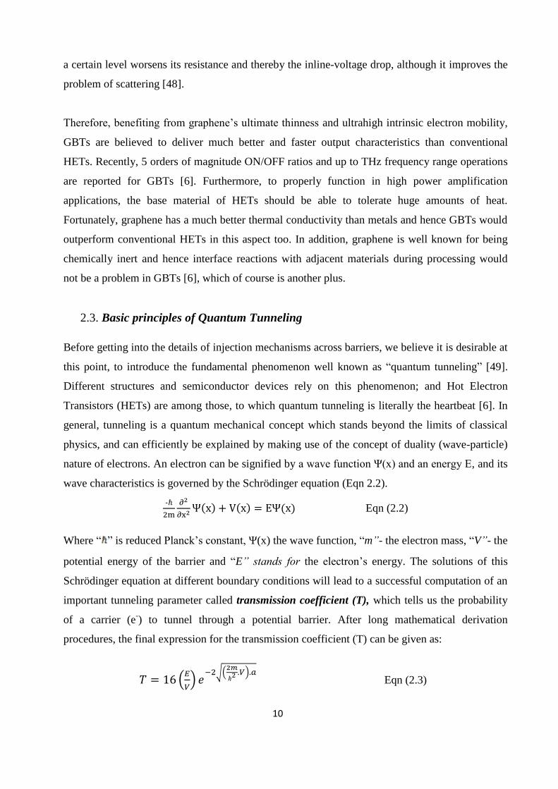
electrons will have a non-zero probability of penetrating the potential barrier and pass onto the
other side, as illustrated in figure 2.5b. This however could sound a mere jock to a classical
physics ear, for the wall is thought as an end (figure 2.5a). An interesting illustration for
comparison of classical and quantum physics theories, can be found in figure 2.6.
Figure 2.6:- Illustration of comparison of classical and quantum physics [Online]
b) Quantum Physics a)
Classical Physics
electron Electric field
barrier barrier
Figure 2.5:- Schematics an electron encountering a potential barrier in a) classical physics theory, b) quantum physics theory [Online]

12
The solution of the Schrödinger equation within the region inside the barrier is given by the
expression under Eqn (2.4). From this expression, one can easily observe the presence of an
exponential decay of the wave function inside the barrier, which is clearly visualized in figure 2.7.
Ψ √
Eqn (2.4)
Where is amplitude of the incident wave.
2.4. Current Injection mechanisms across thin barriers
As already indicated, the main target of this thesis work has been investigation of the vertical
current transfer properties across dielectric materials, which could be potential candidates for
tunneling barriers in GBTs. There is no doubt that tunneling current is the central engine for
graphene-base transistors (GBTs). Hence it is crucial to describe the most common tunneling
mechanisms through thin barriers. Here bellow are the possible transfer mechanisms governing
the current transfer across barriers, and their respective brief descriptions. The mechanisms
include: Direct tunneling (DT), Fowler-Nordheim tunneling (FNT), Thermionic /Schottky
emission (SE), Poole-Frenkel tunneling (PFT) and Trap-assisted tunneling (TAT).
2.4.1. Direct Tunneling (DT)
Figure 2.7:- Incoming wave (Region I), quantum mechanical tunneling with exponential decay of the wave function (Region II) and the transmitted wave (Region III) [49]

13
From the basic principle of quantum tunneling covered in the previous section, we have already
known that electrons would face a potential barrier in traversing from a low to high band gap
medium. And it is another truth that, this barrier deforms and changes shape, in the presence of an
external electric field. This deformation will lead to the situation in which Vox < ΦB, as can be
seen in figure 2.8, where ΦB represents the barrier height and Vox stands for the voltage drop
across the oxide. As a result, incident carriers (electrons or holes) will see a trapezoidal barrier,
which of course is narrower than the case in the absence of external field [49], [50].
Considering this situation for example, for MOS structures with thin oxide layer (i.e. tox < 5nm)
and low oxide fields, electrons will be able to directly tunnel the barrier all the way through, to the
metal electrode’s conduction band [51]. This type of quantum tunneling mechanism is called
direct tunneling (DT), which is shown by a red arrow in figure 2.8.
Bellow is an expression describing the direct tunneling current density (JDT), in Equation 2.5.
(
(
)
) Eqn (2.5)
Where, Eox refers to the field across the oxide, ΦB the barrier height for electrons, Vox represents
the voltage drop in the oxide and B and C are physical parameters [51].
2.4.2. Fowler-Nordheim Tunneling (FNT)
Application of a much stronger external electric field to the previous structure will sufficiently
Figure 2.8:- Illustration of direct tunneling (DT) through the energy band-diagram of a metal-oxide-metal structure. Modified from [49].
DT

14
lean the conduction and valence bands of the dielectric layer. This situation will in turn become a
reason for the oxide barrier width to successively decrease, leaving the effective barrier relatively
narrower [52]. Due to this fact, the Fermi-level electrons will see a triangular barrier in the oxide’s
conduction band, for Vox > ΦB [52]. As illustrated in figure 2.9, the effective barrier width
eventually gets narrower (L L’ L”), since the conduction band of the barrier successively
becomes steeper in response to the increasing applied electric field. Thus, it will eventually
become easier for carriers to tunnel through the triangular barrier with a narrow effective width.
This type of tunneling mechanism is known as the Fowler-Nordheim tunneling (FNT) [52], which
occurs in thicker oxides and demands higher electric fields, compared to direct tunneling (DT).
Making use of the WKB (Wentzel-Kramers-Brillouin) approximation, the Fowler-Nordheim
tunneling model can be developed by solving the non-relativistic, time-independent, one
dimensional Schrödinger equation, for a triangular potential barrier [53]. Hence, according the FN
model, the tunneling current density that flows through a thin dielectric layer as a function of
applied field, can be given as:
[
] Eqn (2.6)
Figure 2.9:- Band diagram illustrating how the FNT barrier becomes narrower when the electric field is increased. The barrier seen by the electron in the metal/insulator interface is triangular [68]
FNT

15
Where is the magnitude of the electric field in the oxide, q the electron charge, m the free
electron mass, the effective electron mass in the insulator, h the Planck’s constant, Φ the
energy-barrier height (which is assumed to be independent of the electric field) [54]. From Eqn
(2.6), one can easily learn the strong oxide field dependence of the FN tunneling current that, and
hence higher oxide field would result in a larger FN tunneling current.
2.4.3. Thermionic/ Schottky Emission (SE)
Electrically charged particles are emitted from a conducting body heated to a sufficiently high
temperature, and can be drawn off by an external electric field. The emitted particles could be
either electrons or ions, depending on the nature of the emitter and the pertaining conditions.
These emitted particles are known as “thermions”, and the process they are obtained through is
generally known as “thermionic emission” [55]. When electrons are thermally emitted in MOS
structures and traverse through the insulating layer in between two conducting electrodes, the
emission is generally termed as Schottky emission(SE) [56].
Rising the temperatures of a structure similar to the ones dealt in the above sub-sections, the
thermal activation will enable electrons to overcome the energy barrier at the interface. As a
consequence, electrons jump directly from the electrode to the insulator conduction band, as
shown in figure 2.10. This type of electron transfer mechanism is what we call
thermionic/Schottky emission (SE), whose prerequisite to happen is higher carrier energy than the
potential barrier.
Given under Eqn (2.7), is an expression defining the Schottky emission current density (JSE), as:
Figure 2.10:- a schematic diagram illustrating a thermally excited electron jumping over an energy barrier, to the conduction band of the oxide, by means of thermionic emission.
SE

16
( √ ⁄
) Eqn (2.7)
Where is the effective Richardson’s constant, q the electronic charge, the barrier height,
is the dielectric constant of the oxide layer, is the Boltzmann’s constant and T is the
temperature in oK [57].
From Eqn (2.7), it is possible to observe the fact that Schottky emission current density strongly
rely on temperature. And it is obvious that this temperature is associated with the energy of the
carriers (i.e. higher temperatures will offer higher average energy to carriers).
2.4.4. Defect Mediated Tunneling (DMT)
For the transfer mechanisms we have discussed so far, we haven’t considered the effects of
defects/traps/interface states. However, oxide defects, trap sites or interface states could be
induced either during the device fabrication processes or due to repeated high-field stress during
electrical characterization [58]; [59]. These induced traps or interface states can therefore act as
mediators and assist the electron transfer process in the oxide. This kind of current transfer
mechanism can in general be referred as defect mediated tunneling (DMT). Poole-Frenkel
tunneling and Trap assisted tunneling are included under this umbrella and here they are
addressed right bellow.
2.4.4.1. Poole-Frenkel Tunneling (PFT)
The precondition for Poole-Frenkel tunneling to occur, is the existence of high density of charged
traps/impurities in the bulk of thin oxides, but thicker enough to suppress direct tunneling [60],
[61]. During the Poole-Frenkel effect, the coulomb potential of charged impurities reduces the
potential barrier height in an external field (figure 2.11b), because of which an enhanced emission
rate occurs at low fields [60].
In case of Poole-Frenkel tunneling, electrons from the electrode’s conduction band undergoes
direct tunneling and reach the first trap site in the localization of the interface, as indicated by the
red arrow in figure 2.11a (assuming that the interface-to-trap distance is very small). This injected
electron will then face a barrier of height Φ , which will eventually be lowered by the coulomb
potential of charged impurities, which resulted from the applied external electric field. As a result,

17
a thermally exited electron will afford to pass over the barrier (thermionic emission) and arrives at
the next trap site. This “trap-detrap” process will repeat until the electron crosses the whole barrier
[62].
The equation which describes the Poole-Frenkel (PF) current density (JPF) is given as:
( √
) Eqn (2.8)
Where is Boltzmann’s constant (eV/K), is the trap depth from the conduction band, q is the
electron charge, is the permittivity of free space and is the dielectric constant [63]. From Eqn
(2.8), one can infer the temperature and electric field dependence of the PF current. As a final tip,
it is worth highlighting here that, during the Poole-Frenkel conduction, the energy an electron
needs to transfer from the localized trap to the conduction band decreases with increasing electric
field. In other words, the higher the electric field, the lower will be the electron escape energy and
hence the lower the activation energy [63].
2.4.4.2. Trap-Assisted Tunneling (TAT)
As the name implies, Trap-assisted tunneling (TAT) in general is a current transfer mechanism in
which electrons are assisted by defects/traps in the oxide, to propagate through the insulating layer
to the conduction band of the electrode. TAT can be of many varieties depending on: the nature,
density and depth of traps from the conduction band; as well as on the conservation of energy of
Figure 2.11:- (a) diagram showing Poole-Frenkel tunneling; and (b) barrier lowering by the columbic potential of impurity charges as a result of an applied external field in PF effect [modified from online source]
PFE
DT

18
electrons during the process. Some of these varieties could be: “elastic and inelastic trap assisted
tunneling” [64], “single trap and multi-trap assisted tunneling” [64] and “shallow-trap and deep-
trap assisted tunneling” [65].
The existence of defects in the oxide would literally split the traverse length in to two or more
parts, making electrons feel like they progressively face thinner barriers at a time, and undergo a
two (or more)-step tunneling. i.e. following the applied gate-voltage, electrons will be injected
from the 1st electrode’s conduction band directly to traps in the oxide, and then from the traps they
tunnel to the 2nd
electrode conduction band [65]. Single-trap elastic and inelastic TAT processes
are elaborated in figures 2.12 (a & b), respectively.
For very thin oxides, only a single-trap could be considered to model the TAT current. For thicker
oxides however, one-trap may not be good enough to produce tunneling current and hence multi-
trap model shall be used [64]. This is due to the fact that, presence of several traps in the oxide
would generate a way in the barrier, for electrons to tunnel through. The inelastic TAT process can
occur during both single and multi-trap TAT processes, as shown in figures 2.13a & b, respectively.
Multi-trap assisted tunneling process commonly occur in thicker and highly degraded (high defect
density) oxides (figure 2.13 b), where electrons can have several options during the transfer. In this
case, electrons can also undergo hopping, from trap to trap until they reach the conduction band of
the destination electrode [65].
Figure 2.12:- a) elastic TAT (without energy loss) and b) inelastic TAT (with energy loss ∆E), modified from [68]

19
The Trap-assisted tunneling current density can be described by the expression in Eqn (2.9)
as:
( √
) Eqn (2.9)
Where refers to mass of electrons in the oxide, is electric field in the oxide, is the trap
depth from the conduction band, q is electron charge and h represents the Planck’s constant. q
Will give the trap energy level [57].
Figure 2.13:- The process of Inelastic: a) single trap-assisted tunneling including a sole trap (the excess energy of the tunneling electron is released by means of phonon emission) [64]; and b) ) Multi-trap assisted tunneling ( the trap and de-trap times to and from the trap, the tunneling rate of a specific trap) [64].

20
3. Device Fabrication
In this thesis project, we have gone through two batches of device fabrications utilizing the wide-
range of state-of-the-art facilities, in the KTH’s world class micro and nano fabrication clean
room laboratory. During the first batch, Metal-Oxide-Semiconductor (MOS) capacitor structures
with seven distinct dielectric materials were fabricated in wafer-scale fabrication processes. Based
on the characterization results of these first batch devices, dielectrics with better performances
were selected and used as bottom gates in Graphene-Field-Effect-Transistor (GFET) structures,
which we fabricated during the second batch fabrication process. The details of the overall
fabrication process will be reported in this chapter.
3.1. Fabrication of MOS Capacitor Structures
As highlighted in the entrance, the main objective of fabricating these structures had been
evaluation of different dielectrics, to find out those that are good candidates for use as tunneling
barriers in our next structures. To make this a reality, we have used seven different dielectric
materials and successfully fabricated fully functional MOS capacitor structures, on wafer-scale.
3.1.1. Substrate preparation
We started the fabrication process with seven, 4-inch n-type silicon wafers as substrates. To
discard particles, dissolve metal impurities and remove any unwanted organics from the surfaces
of the wafers, we have began the process by employing a standard IMEC-clean procedure [66].
Then the wafers were dried with nitrogen gas and get ready for the upcoming dielectric / high-k
dielectric deposition process, which is described below.
3.1.2. Thin dielectric layer formation
In our MOS capacitor fabrication process, deposition of thin dielectric layers seems to be a very
fundamental and critical stage, which determines the fate of the end device. Producing high
quality oxide layers of low defect density demands a high standard deposition technique with:
high efficiency, precision, conformality and good thickness control. Atomic Layer Deposition
(ALD) is a Chemical Vapor Deposition (CVD) technique with sequential and autonomous gas-

21
solid reactions [67] and it is highly pronounced for its capability of producing quality oxides.
Hence in developing our MOS structures, we have used ALD technique to deposit good quality
oxides, (except for SiO2 which was thermally grown in the oxidation furnace). We carried out the
deposition process in “BENEQ TFS 200” ALD tool (figure 3.1), in KTH’s clean room lab.
Figure 3.1:- a photograph of the KTH clean room lab, “BENEQ TFS 200” ALD tool with labeled parts
Deposition parameters and specifications for deposition of the seven dielectric layers of our MOS
structures are given in table 3.1 bellow. Type of precursor materials, ALD deposition rates and
recipes used for the deposition processes, is also reported in table 3.2.
Table 3.1:- Deposition facts for the dielectric layers formed during the MOS capacitor structures
fabrications.
Dielectric
Type
SiO2 HfO2 TiO2 Al2O3 SiO2/HfO2 SiO2/Al2O3 TiO2+Al2O3
”mix” (1:1)
Deposition
Technique
Thermal
Growth
ALD ALD ALD ALD ALD ALD
Reactor
Temp(oC)
900 300 200 200 300 300 300

22
Deposition
Cycle
6 min 170 100 50 Ozone clean
170 (HfO2)
Ozone clean
45 (Al2O3)
1:1
30
Thickness
(Å)
48 51 27 - 30 52 60 60 44
3.1.3. Top and back contact formations
The top contacts of our MOS structures were made of Titanium Nitride, which sometimes known
as “Tinite” (TiN). To deposit about 100Å (10nm) TiN layer, we run 400 ALD cycles at a rate of
0.024 nm/cycle at a reactor temperature of 350oC. The precursors we used for this deposition can
be referred from table 3.2. For back-contact, we deposited a very thin Nickel (Ni) layer by
sputtering; and that is intended for securing an Ohmic contact to the silicon bulk, which will be
grounded during electrical measurements.
Table 3.2:- ALD deposition details (specifications) used during the MOS capacitor fabrications.
Recipe
Run
Precursors
Used
Temp. (oC) Deposition rate
(nm/ Cycles)
HfO2-thermal
HS1
P1- Bis (methylcyclopentadienyl)
Methoxymethyl hafnium:HfDO4 (liquid)
P2- DI-Water: H2O (liquid)
350
0.03
TiO2-thermal
P1- Titaniumtetrachloride:TCl4 (liquid)
P2- DI-Water: H2O (liquid)
200
0.053
Al2O3-thermal
P1- Trimethylaluminum(TMA):Al2(CH3)6
(liquid)
P2- DI-Water: H2O (liquid)
200
0.11
TiO2+Al2O3
“mix”-thermal
1:1 pulse ratio
P1- Titaniumtetrachloride:TCl4 (liquid)
P2- Trimethylalumi(TMA):Al2(CH3)6 (liquid)
P3- DI-Water: H2O (liquid)
300
0.163
TiN-thermal
P1- Titaniumtetrachloride:TCl4 (liquid)
P2- Ammonia: NH3 (gas)
350 0.024

23
3.1.4. Patterning/Photo lithography
Once we finished the top and back contact depositions, we defined the patterns/structures of our
devices by accomplishing “Photolithography”. In doing so, the wafers were coated with a positive
standard photo resist (SPR 700-1.2) and then pre-exposure baking was done @ 90oC for 1 minute,
using “MAXIMUS 804” photo-resist coating and developing tool. The exposure was then done in
“XLS 7500/2145 i-line stepper” lithography tool, in which only part of the resist in areas where
we do not want TiN, are exposed. The exposed wafers were soft-baked @ 110oC for 1 minute and
then developed back in “MAXIMUS 804”, where “MFCD26” was used to remove the exposed
resist. Afterwards, a 110oC hard bake was done for 25 minutes, which was meant to further
harden the unexposed resist so that it would act as a mask to protect the TiN layer underneath,
during etching. As next step, a Reactive-Ion-Etching (RIE) technique was carried out to remove
the uncovered TiN layers. Finally, the photo resist was stripped in an “Oxygen plasma barrel”,
where the plasma burns the photo-resist remained on top of the TiN contacts. With that, we
finished fabrication of our fully functional MOS structures, whose schematics and microscope
image are presented in figures 3.2a & b, respectively.
3.1.5. Summary
The overall fabrication process for the MOS capacitors can be summarized as follows: The
Silicon wafers were first cleaned, after which SiO2 thermal growth and high-k dielectrics ALD
deposition, followed by TiN contact formation were accomplished. Nickel was then sputtered for
(a) (b)
Die
lect
ric
laye
r
TiN
, to
p e
lect
rod
e
Figure 3.2:- (a)-Schematics of a MOS Capacitor and (b)-microscope picture showing top-view of a real MOS capacitor structure under microscope
Ni
n-Si
Dielectric
layer
TiN gate electrode

24
back contacting, and photolithography process was carried out to define the TiN contacts. Next,
an RIE was carried out to complete the patterning process and finally the resist was stripped. The
flow-chart in figure 3.3 illustrates the main process flow for this fabrication process.
Figure 3.3:- Schematic diagram summarizing the fabrication process flow carried out during fabrication of the MOS capacitors
3.2. Fabrication of (BG-GFET) Structures
After evaluating the seven dielectric materials in the MOS structures from the first batch
fabrication, we selected some of them which we believed were good enough to serve as tunneling
barriers in Graphene Field Effect Transistor (GFET) structures. In this fabrication round, four
different gate dielectrics (SiO2/HfO2, SiO2/”Al2O3+TiO2 mix”, ”Al2O3+TiO2 mix” and TiO2) of
more or less similar thicknesses, and SiO2 of three different thickness (i.e. 2nm, 5nm and 10nm),
were used to develop the transistor structures. That would comprise a total of seven device groups
that we have fabricated in this round.
Unlike the first batch fabrication, we run this fabrication process chip-by-chip, for a total of 27
chips. We dedicated four chips for each group (two for graphene under and two for graphene on
top of contacts). Just like the first batch, this second batch was also a successful fabrication
process, which led to the demonstration of working devices from all intended categories.
Fabrication details of these devices will explicitly be covered under this section.

25
3.2.1. Substrate descriptions and preparations
The starting substrates that we built our BG-GFETs on, were manufactured on a wafer scale
production, by IHP in Germany [68]. IHP made the substrates in such a way that, high grade thin
SiO2 tunneling barriers were grown on top of very thin doped silicon (n Si) region. That defines
the rectangular active regions of different areas, orientations and thicknesses (2nm, 5nm and
10nm). Besides, those active regions were isolated from one another by about 400nm thick
shallow trench isolation (STI), which is made of low grade undopped silicon glass (USG).
The back sides of the wafers were coated with silicon nitride (SiN) and to protect their front side
surface, we coated the wafers with resist layer. The wafers were then diced in to (1cm x 1cm)
chips and then right before the Nickel (Ni) back contact deposition, the back side SiN layer was
dry-etched for 2 minutes. The resist on the chips’ surfaces was also cleaned using: Acetone >>
Isopropanol >> DI-water sequentially, just before ALD deposition. In addition, for some of the
chips where we deposited ALD oxide directly on Si, we first etched the 2nm IHP-produced SiO2
layer, using a 3:1 diluted buffered hydrofluoric acid (BHF), with an established rate of 0.5nm/sec.
3.2.2. Thin High-k dielectric deposition
What we have done here, is technically pretty much similar to what has been described in section
(3.1.2), except the fact that some optimizations were made on the deposition parameters as can be
observed in (table:-3.3). Hence, one can refer back to section (3.1.2) if there would arise the need
to get the feeling of what we have gone through, at this process stage.
Table 3.3:- ALD deposition facts for the bottom gate materials of the fabricated BG_GFET structures
Bottom Gate
(dielectric) Type
Stack of HfO2
on 2nm SiO2
Stack of
TiO2+Al2O3 ”mix”
on 2nm SiO2
TiO2+Al2O3
”mix”
TiO2
SiO2
Deposition
Technique
ALD
(HfO2)
ALD
(TiO2+Al2O3 ”mix”)
ALD
(1:1)
ALD Made by IHP
Deposition Temp.
(oC)
350 200 230 200 NA

26
Deposition Cycle 135 26 35 140 NA
Thickness (Å) 45 42 60 66 20, 50 & 100
3.2.3. Graphene Transfer
As explicitly mentioned in the entrance of this chapter, we had seven groups of devices with each
group having two sub-groups, for graphene under and graphene on top of contacts. For devices
with graphene under contacts, the process step right after gate deposition was graphene transfer.
However, graphene transfer had been the very last step for devices with graphene on top of
contacts. The graphene transfer process in general was a seemingly easy but practically
challenging task of the overall fabrication process. It is a time consuming process, which is very
sensitive and is very easy to mess-up. Despite those challenges, we have successfully transferred
single atomic-layer graphene on to a total of 27 substrate chips. More interestingly, we have
confirmed through electrical characterization that, 25 of them were fully functional.
The graphene we used was a CVD-graphene-on-Cu (section 2.2.1) produced in such a way that,
graphene was grown on both sides of the copper foil. Hence, our first task was to remove the
graphene layer on one side of the Cu sheet. We did that by first coating the other side graphene
layer with a “PC” (“Polybisphenol A carbonate”) polymer layer and then did 40 seconds of a
selective RIE graphene etch in the “Plasmalab80Plus (Oxford RIE System)”dry etching tool. The
polymer coating in fact was meant to protect the-to-be transferred graphene layer from the RIE
etch, to guard it from any harm during the proceeding processes and also to make handling it
easier during transfer.
Cutting the graphene/polymer stack in to pieces of compatible sizes to our chips, we then removed
the copper foil with a wet etching process using “Ferric chloride” solution (FeCl3 6% by mass),
for about 60 to 90 minutes. Once all the Cu is gone, we cleaned up the chips in a 3:1 diluted
“Hydrochloric acid” (HCl 37%) for about 10 minutes, which later was rinsed by “DI-Water”.
Using a well cleaned carrier chip, we then very gently transferred the Graphene/Polymer stack
onto target substrates (chips). Having made sure that the transfer was appropriate, we evaporated
the water in the “graphene-substrate” interface by heating up the chips on a hot plate @50oC for
6-8minutes, and of course cooled them down afterwards, before the next procedure.

27
Removing the protective polymer layer on top of graphene being our last task, we treated the
chips in Acetone (C3-H6-O) for about 5 minutes and then put them in “Chloroform” (CHCl3) for
almost overnight. In the end, we cleaned the chloroform with Isopropanol (C3-H8-O) followed by
DI-Water. At this stage, the chips were ready for the photolithography process, which will be
covered under the next section. From figure 3.4, one can find a clear summary of the graphene
transfer process with schematic diagrams.
3.2.4. Patterning / Photo-Lithography
We have executed two rounds of patterning/photo-lithography during this fabrication process. The
first one was done for patterning the transferred graphene, while the second was done to define the
S/D contact areas where the Ti/Au contacts will be formed. In order to pattern the graphene layer,
we first coated the graphene surface with a thin layer of standard positive photo resist (SPR700-
1.2) in the “OPTIspin SST20” spinner, followed by a pre-exposure bake for 1min at 90oC. The
chips were then aligned with alignment marks one chip at a time, and exposed for 5.9sec in the
contact lithography machine – “Mask aligner MA6/BA6 Karl Suss” (figure 3.6). To proceed, we
do soft baking of the exposed chips at 110oC for 1 minute on a hot-plate and then developed them
in “MFCD26” for 30 seconds followed by DI-water rinsing. Following that, the rinsed dry chips
were hard baked for 25 minutes in a 110oC oven; and then RIE graphene etch was done in
“Plasmalab80Plus (Oxford RIE System)”. That left the graphene layer perfectly patterned in a
way that, graphene is only on the active area, right above the gate oxide and slightly extended to
Figure 3.4:- Schematic diagram illustrating the process flow for graphene transfer process.
LG

28
both sides to overlap with the edges of Source/Drain contacts. A simple schematic diagram
illustrating this can be seen below, in figure 3.5.
Figure 3.5:- Schematic diagram showing the extents of graphene after graphene is etched (patterned)
Figure 3.6:- Photograph of the “Mask aligner MA6/BA6 Karl Suss” photolithography machine, with labeled components
The second lithography round, which was done to define the S/D contact areas, was exactly the
same as the first. The only difference was that, in the second round, we had a light-insensitive
polymer “LOR 5A” under the standard (SPR700-1.2) resist and baked it @ 165oC for 2 min and
30 sec. Right after development and hard bake step, (20nm/50nm) Ti/Au was deposited and then
lift-off was done as a final step. During the lift-off process, the chips were submerged in a beaker
of “1165-remover”, being heated up @ 80oC on a hotplate with the magnetic spinner ON. Finally
we ended the patterning process by cleaning up the chips with DI-water. After lift-off, the devices
look like the one shown in figure 3.7, in next section.

29
3.2.5. Back and Top-Contact Formations
For contact formation, we employed the electron beam physical vapor deposition (PVD)
technique for which, we used “Provac PAK 600 Coating System”, which is a metal evaporation
tool. Actually we had two separate metal evaporation sessions, for we had two types of contact
formations: the back- and Drain/Source top-contacts. For the sake of maintaining an Ohmic
contact to the bulk silicon during electrical measurements, we evaporated 15nm of Nickel at the
backside of the chips, after the SiN etch and before the ALD oxide deposition. Having gone
through the lithography/patterning process of defining the Source/Drain contact areas, we
deposited 20/50 nm Ti/Au. If one wonders why we used Titanium (Ti) underneath gold (Au), it is
just because that, Ti is far more adhesive to oxides than Au is [69]. After the Ti/Au deposition, we
did “lift-off”, which concludes the S/D contacts formation. Figure 3.7b, displays the top-view of
the final device, where the S/D contacts are clearly visible. For devices with graphene on top of
contacts, we transferred graphene on top of the contacts and then did one more lithography round
followed by RIE graphene etch. With this, we ended the overall fabrication process of the seven
different device groups of BG-GFET structures.
3.2.6. Summary
After preparation of substrates, gate formation was done by depositing varity of thin oxide films
(table 3.3) in ALD. A single layer Graphene was then transferred onto substrates with the ALD
oxides, one chip at a time. Afterwards, the graphene layer was patterned using a round of
(a)
Figure 3.7:- (a) Schematic diagram showing structure of a BG-GFET structure [76]; and (b) top-view of the fabricated BG-GFET under microscope (Note: a very light, white shade is added on top of the oxide, just to visualize the transparent graphene layer)
(b)
Gra
ph
en
e
STI
Gate Oxide
Ti/Au, S/D contacts

30
photolithography followed by RIE. Similar way, a second round lithography but now followed by
lift-off, was committed to define the Source/Drain contact areas. The standard (700-1.2) positive
photo resist was used for graphene patterning lithography, whereas the polymer (LOR 5A) layer
was added underneath, for lift-off. The devices were fabricated successfully this way, and were in
a very good shape for electrical characterization, which will be covered in the next chapter. The
overall fabrication process flow of our BG-GFET structures is briefly illustrated by the
combination of schematics in figure 3.9 and process flow-charts shown in figures 3.10 & 3.11. In
addition, top-view of the microscope picture of a final BG-GFET structure can also be seen
below, in figure 3.8.
S/D (Ti/Au) S/D (Ti/Au)
SiO2 Bottom-gate
Graphene STI
Figure 3.8:- Microscope picture of top-view of the fabricated BG-GFET structure

31
STI
Figure 3.9:- Schematic diagrams, showing fabrication process steps for devices with (a) graphene under; and (b) graphene on top of contacts.
Step 1- Ni-back contact
deposition Ni
Ti/Au SLG SLG
Lith
o
(a) (b
)
LOR 5A/700-1.2 (stack)
Lith
o
For d
evices with
graph
ene o
n to
p o
f
con
tacts LOR 5A/(PR700-
1.2) stack
Ti/Au
Lith
o
S/D S/D
RIE Graphene -Etch
Lift Off
Single Layer Graphene
Transfer
PVD Ti/Au Contact
deposition
Lithography: LOR 5A/ PR 700-1.2
stack
Lith
o
Lith
o
Graphene
Single Layer Graphene
Transfer
Lift Off
PVD Ti/Au deposition
Lithography -LOR 5A/ PR 700-1.2
stack
RIE Graphene-Etch
For d
evices with
graph
ene u
nd
er
con
tacts
Step 2- ALD High-k
deposition
ALD Oxide
Si
STI STI SiO2
Ni Ni
n+ Si
SiO2 n+ Si
ALD oxide ALD oxide
Si
n+Si
Si
ST
I
ST
I
2nm SiO2

32
Figure 3.10:- Process flow showing the fabrication process for devices with graphene under contacts.
Back-contact Deposition
(PVD)
High-K Deposition
(ALD)
Graphene Transfer
Photo Lithography
Graphene Etch (RIE)
Photo Lithography
S/D Contact Deposition
(PVD)
Lift Off
.

33
Figure 3.11:- Process flow showing the fabrication process for devices with graphene on top of contacts.
4. Characterization
Apart from assessing important and relevant literatures to our area of interest, characterization had
been the major part of this experimental work, of course next to device fabrication. It has been the
key tool to inspect our processes and see the fruit of our great work in the end. Thinking of all the
useful informations it offered us about our devices, we would say, characterization in general is
our voice, because of which we are communicating our work to the world. In this chapter, we will
highlight some of the useful characterization techniques that we utilized throughout our
experimental work.
4.1. Ellipsometry
It was so important for us to get the feeling of physical thicknesses of our ALD deposited
dielectric materials. Hence, we used a metrological technique called “Ellipsometry”, for which we
used the “Horiba UVISEL ER”- Ellipsometre tool. In the beginning, the fact that the samples we
got from IHP were already patterned (i.e. the small active areas were already defined, being
Back-contact Deposition
(PVD)
High-K Deposition
(ALD)
Photo Lithography
S/D Contact Deposition
(PVD)
Lift Off
Graphene Transfer
Photo Lithography
Graphene Etch (RIE)
.

34
surrounded by the STI), made it so hard to locate the UV light beam perfectly on the small active
areas, without being affected by the reflectance from the thick STI. However, this problem was
later solved by using dummy chips, which we run in the ALD together with the corresponding
samples we intended to know their thicknesses. Therefore, the thickness values we have presented
in Tables 3.1 and 3.3 were measured by this technique.
4.2. Raman Spectroscopy
After graphene transfer, Raman Spectroscopy was carried out to insure the presence and quality of
the graphene layer we transferred onto the substrate chips. And the Raman Spectroscopy result
has shown sharp 2D- and G-band peaks (figure 4.1), which confirms the presence of a good
quality graphene layer on our chip.
Figure 4.1:- Raman shift with sharp 2D-band peak. The Raman spectroscopy confirms the single layer graphene we transferred [69]. The inset shows the position of the laser beam on the graphene layer.
4.3. Electrical Measurements and Measurement setups
It would not be exaggeration to say that, the overall project work relies on electrical
characterization. Using this technique, we have made extensive measurements on our devices and
35
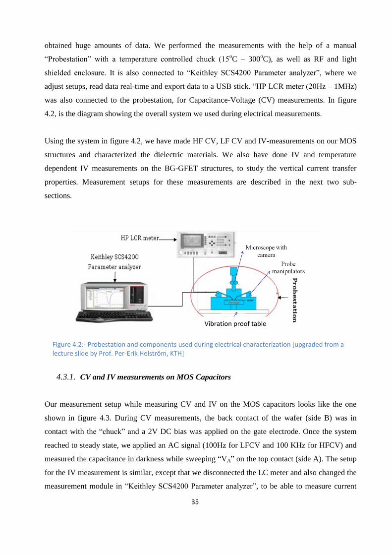
obtained huge amounts of data. We performed the measurements with the help of a manual
“Probestation” with a temperature controlled chuck (15oC – 300
oC), as well as RF and light
shielded enclosure. It is also connected to “Keithley SCS4200 Parameter analyzer”, where we
adjust setups, read data real-time and export data to a USB stick. “HP LCR meter (20Hz – 1MHz)
was also connected to the probestation, for Capacitance-Voltage (CV) measurements. In figure
4.2, is the diagram showing the overall system we used during electrical measurements.
Using the system in figure 4.2, we have made HF CV, LF CV and IV-measurements on our MOS
structures and characterized the dielectric materials. We also have done IV and temperature
dependent IV measurements on the BG-GFET structures, to study the vertical current transfer
properties. Measurement setups for these measurements are described in the next two sub-
sections.
4.3.1. CV and IV measurements on MOS Capacitors
Our measurement setup while measuring CV and IV on the MOS capacitors looks like the one
shown in figure 4.3. During CV measurements, the back contact of the wafer (side B) was in
contact with the “chuck” and a 2V DC bias was applied on the gate electrode. Once the system
reached to steady state, we applied an AC signal (100Hz for LFCV and 100 KHz for HFCV) and
measured the capacitance in darkness while sweeping “VA” on the top contact (side A). The setup
for the IV measurement is similar, except that we disconnected the LC meter and also changed the
measurement module in “Keithley SCS4200 Parameter analyzer”, to be able to measure current
Figure 4.2:- Probestation and components used during electrical characterization [upgraded from a lecture slide by Prof. Per-Erik Helström, KTH]
Vibration proof table

36
instead of CV. In this case, we set VB at 0V and swept VA to measure IA as a function of VA.
4.3.2. IV and Temperature-dependent IV measurements on BG-GFETs
Here, we have used the “Keithley SCS4200 Parameter analyzer” connected to the probestation.
We have used a 2-probe setup (figure 4.4a) while performing the standard IV and temperature-
dependent IV measurements. On the other hand, the three-probe setup (figure 4.4b), was used to
measure devices in GFET mode; i.e to measure the “Transfer characteristics” (drain current Vs
back-gate voltage) and “Leakage characteristics” (back-gate current Vs back-gate voltage). In the
case of temperature-dependent IV, a heat generator was used to heat up the sample stage to
intended temperature levels. This way, we measured the current with a temperature gradient of 15
oC – 30
oC, the lowest temperature being 25
oC and the highest 200
oC.
Figure 4.3:- schematic diagram showing measurement setup used during CV and IV measurements on MOS capacitor structures.
Ni
n-Si
Dielectric
layer
TiN gate electrode
B
A
VG

37
Using the “two-probe” setup (figure 4.4a), we measured the current on the top (S/D) contact,
while biasing the chuck at 0V and sweeping the voltage on the S/D contact, either from zero to
positive or from negative to positive values, depending on the type of data we needed. On the
other hand in the GFET mode shown in figure 4.4b, we applied a source-drain voltage (VDS) of
1mV and varied the voltage on the chuck. Then we measured the drain current (ID) and back-gate
current (IBG) as a function of the varying back-gate voltage (VBG), to obtain what we call the
“transfer”- and “leakage- characteristics”, respectively. All the data obtained through electrical
measurements were then processed and analyzed in a computer program called “Origin lab”,
where we produced all the plots included in this thesis report. All those final results will shortly be
presented in the form of variety of plots and be exhaustively discussed in the forthcoming chapter.
5. Presentation and Discussion of Results
Large amount of electrical data were acquired from the electrical measurements carried out on the
MOS capacitors and BG-GFET structures. Further processing and analysis of these data have
been accomplished using “Origin lab” data processing software. In result, several plots and graphs
were produced, which will be presented and discussed in this chapter.
5.1. CV- Characteristics of the MOS Capacitors
Figure 4.4:- Schematic diagrams illustrating: (a) two-probe setup used during standard IV measurement on BG-GFET structures. Here, the current is measured on the top contact where the voltage is swept, while the back contact is biased at 0V. (b) three-probe setup used to measure the current on drain while sweeping the back-contact voltage, at a drain source voltage (VDS) of 1mV.
(a) (b)
S/D ALD Oxide
Graphene
n+Si
Si
STI 2nm SiO2
Ni
ALD Oxide Graphene
n+Si
Si
STI
2nm SiO2
Ni

38
As clearly stated in the previous chapter, IV and CV measurements were done on our seven
varieties of MOS capacitors. The resulting high-frequency CV (HFCV), low-frequency CV
(LFCV) and current-voltage (IV) plots are presented in figures 5.1a, 5.1b and 5.2, respectively.
The low-frequency CV curves shown in figure 5.1b are very noisy and hence didn’t yield as such
useful information. In fact, due to the high level of noise arising as one goes to low frequency
ranges, obtaining the low frequency capacitance of MOS-Cs from CV measurement is known to
be almost impossible [70]. The HF CV curve (figure 5.1a) on the hand, displays well behaved CV
curves, at least for the commonly used oxides (SiO2, HfO2, TiO2 and Al2O3). Hence, together with
the corresponding IV results, it somehow helped us to make qualitative comparison among those
dielectrics. However, the values in the HF CV curves were still not precise enough to be used for
quantitative purposes, for the extracted parameters of known oxides had shown some deviations
from standard literature values. That deviation could actually be attributed to the serious
resistance effects, which somehow could be minimized by making some sort of analytical
corrections. Moreover, in principle for good HFCV results, higher frequencies > 1MHz are
normally recommended so that interface traps would not respond [70]. However in our case, it
was not possible to reach the recommended frequency range due to the fact that 1MHz was the
roof for the instrument we used (section 4.3). Even below 1MHz, we faced a trade-off between the
level of frequency and level of quality-factor (Q). i.e. increasing the frequency resulted in low
quality factor values (< 20) and in raising the quality fact to the recommended value (Q 20),
Figure 5.1:- Measurement results of MOS capacitors in the form of: (a) HF CV measured at 100 KHz and (b) LF CV measured at 100Hz, which has a high level of noise. The inset in (a) illustrates the structure and measurement setup of the MOS Capacitor structures.
TiN
(a) (b)

39
caused the frequency to reach low range. Hence, the measurement results presented here, are the
best they could be although we could not use them to extract quantitative data.
5.2. IV- Characteristics of the MOS Capacitors
We have measured both the hole and electron currents for the MOS capacitors under study, and
the resulting IV-characteristics plots are shown in figure 5.2. This graph has clearly delineated
reasonable IV responses of the dielectric materials used. Hence, it was very useful for us to make
comparison among those dielectric materials.
Figure 5.2:-IV measurement results from MOS capacitors, with both hole and electron currents and the table to the right presents the corresponding thicknesses of the oxides used. The curves in general lack symmetry and that could be due to the work function difference of the n-Si and TiN on either side of the oxides. The graph also shows that TiO2 which has the lowest band offset is the most leaky and the largest band offset material-SiO2 is the least leaky one. Moreover, Al2O3 and SiO2/Al2O3 stack have the highest amount of traps.
Oxide tOX (nm)
SiO2/HfO2 6
SiO2/Al2O3 6
SiO2 4.8
HfO2 5.1
TiO2 2.7 - 3
Al2O3 5.2
TiO2+Al2O3
”mix”
4.4

40
To enable comparison of our results with literature, we have sketched the conduction band-offset
(CBO) and Valence band-offset (VBO) of the four main oxides, with respect to the conduction
and valence bands of silicon, respectively (figure 5.3).
Figure 5.3:- a schematic diagram illustrating the conduction and Valence band offsets of SiO2, Al2O3, HfO2 and TiO2 with respect to the conduction and valence bands of Si, respectively. The CBO and VBO values are taken from reported values in available literatures.
As one can see from figure 5.2, TiO2 and SiO2 are found to be the leakiest and the least leaky
oxides respectively, which also matched with available literatures (figure 5.3, for positive
voltage). On the other hand, considering figure 5.3, it seems that HfO2 and Al2O3 have
interchanged places in the IV plot. But this could be caused by the higher trap density of Al2O3
[70] and it is known that the presence of more traps creates more chances for electrons to tunnel
through the oxides.
In addition, according to our results, the oxide stacks (SiO2/HfO2 and SiO2/Al2O3) happen to be
leakier than their single-layer equivalents (SiO2, HfO2 and Al2O3). And this could arise from the
fact that, the SiO2 layer in the stacks is extremely thin and is not thermally grown; it rather is
obtained from the ozone treatment of silicon during the “Ozone-clean” ALD process. The exact
thickness of this layer is not known, but in principle it should be around 1nm and hence electrons
can directly tunnel through this ultrathin layer to reach to the stack-interface. Moreover, the
addition of one more interface in the stacks (which the single-layer oxides do not have), could
host additional interface states, which in turn could establish additional path for electrons to
somehow transfer through the barrier of the next oxide layer. Hence, in comparison to the single
oxide layers, the stacks seem to have additional current transferring mechanisms and thus the
early and yet higher currents in the stacks could be originated from these facts.

41
5.3. IV-Characteristics of the BG-GFETs
After processing IV data obtained from “two- and three-probe” measurements, here in this section
we are presenting results in the form of “transfer & leakage characteristics” plots.
5.3.1. Transfer characteristics
Studying the lateral transport properties was not actually part of the main concern of this thesis
project; it is rather the vertical transport which we were devoted to investigate. However on the
way, we have also made GFET-mode measurements on our devices to make sure that we had a
properly functioning graphene layer covering the gate. Figure-5.4 presents the transfer
characteristics of BG-GFETS with SiO2 bottom gates of different thicknesses, measured at a
source-drain voltage of 1mV. From the figure, one can clearly see the minimum conductivity
points (Dirac points), which indicates the ambipolar behavior of our BG-GFETs, which arised
from the gap-less nature of graphene. This tells us that our devices are operating just like typical
GFETs and this proved us the existence of good quality graphene layer on top of the SiO2 gate.
Figure 5.4:- Transfer Characteristics of 2nm, 5nm and 10nm SiO2 bottom gates, at drain-source voltage of 1mV. The inset shows the schematics of the cross-section of the device. The Dirac points except for 10nm SiO2 are more or less located around 0V. The curves are smooth and show good current modulation with the changing field. However, the asymmetry could have resulted from chemical adsorbants incorporated during fabrication and any charged molecules in the air interacting with carriers of the graphene, which was left open.
Ni Si
SiO2 n
+ Si STI
SLG
VBG = Swept (from – to +)
VDS = 1mV

42
The transfer characteristics of BG-GFETs with the rest four bottom-gate oxides (2nm/4.5nm
SiO2/HfO2 stack, (2nm/ 4.2nm) SiO2/ “Al2O3+TiO2 mix”, 6nm “Al2O3+TiO2 mix” and 6.6nm
TiO2) can be found in figure 5.5. Unlike the previous one, this “transfer characteristics” have
displayed a set of asymmetric and non-smooth curves with Dirac points slightly shifted towards
the negative voltages.
Figure 5.5:- Transfer Characteristics of BG-GFETS with 2nm SiO2/4.5nm HfO2, 2nm SiO2/4.2nm "Al2O3+TiO2 mix", 6nm "Al2O3+TiO2 mix" and 6.6nm TiO2 bottom gates; and measured at VDS = 1mV. The right inset shows the schematic structure of BG-GFETs with TiO2 and “TiO2+Al2O3 mix”, while the left is for the stacks. The Dirac points in general have shifted to around -1.5V and the curves are not symmetrical and also not smooth except for SiO2/HfO2. This in fact could be caused by: chemical adsorbants, poor graphene/oxide interface resulting in high interface state density and also the fact that graphene is left uncovered.
The Dirac point shifts could actually be resulted from the relatively poor quality graphene/ high-k
dielectric interfaces, where charged impurities might have been incorporated. Moreover, due to
this possible poor interface, the graphene layer may not completely be adhered to the oxide
surfaces and that in turn could result in graphene being torn or pinched off randomly. As a
consequence, the effective graphene surface in contact with the drain and source contacts may not
be similar. Thus, a difference in contact resistances could arise, and that could have caused the
asymmetric and non-smooth transfer characteristics [71].
SLG
SiO
2
TiO2 or ”mix”
STI
Si Ni
Ni Si
n+ Si STI

43
One should also remind the fact that, the graphene layers in our devices are uncovered, giving the
chance for any ions or charged air molecules to interact with graphene’s charge carriers and
distort the electrical transport properties [69]. Moreover, it should also be noted that the Dirac
point shifts and current asymmetries could have originated from the “chemical doping of
adsorbents” induced during processing [72]. From the discussions so far, one can draw a wise
conclusion that, graphene has a much better interface with SiO2 than with the high-k oxides
(Al2O3, TiO2 and HfO2). But among these three high-k dielectrics, graphene seem to have a
relatively better interface with HfO2.
5.3.2. Leakage Characteristics
The IV-Characteristics plots for BG-GFET structures with SiO2 bottom gates of three different
thicknesses are presented in figure 5.6, bellow. From these plots, it is straight forward to see that
the thinnest oxide (i.e. 2nm SiO2) is the most leaky and the thick (10nm) SiO2 bottom gate is the
least leaky one. The results also have displayed higher current levels for positive voltages, which
seem to result from the fact that holes would face a relatively higher barrier than electrons as can
be seen in figure 5.3, and could also arise from the work function difference between the n-Si on
one side and Ti/Au on the other side of the oxides.

44
Figure 5.6:- Leakage characteristics of BG-GFET structures with 2nm (red), 5nm (green) and 10nm (blue) SiO2 bottom gates, where the level of leakage increases as one goes from the 10nm to 2nm SiO2. The IV curves, especially for the thicker ones are not symmetrical at all and this could be due to the fact the difference in the work function of the materials on either sides of the oxides (i.e. n-Si and Ti/Au).
In figure 5.7, we have presented similar plots (measured with similar set ups and plotted similar
ways) for BG-GFETS with (2nm/4.5nm) SiO2/HfO2, (2nm/ 4.2nm) SiO2/"TiO2+Al2O3 mix”,
6nm "TiO2+Al2O3 mix" and 6.6nm TiO2 bottom gates. According to this figure, on the basis of
increasing leakage, these four bottom gate dielectrics can be ranked in the order of: TiO2,
SiO2/HfO2 stack, "TiO2+Al2O3 mix" (1:1 ALD pulse ratio) and finally the SiO2/ "TiO2+Al2O3
mix" stack. That is just based on what we can see from the available plot, but we believe that it is
also good to put in consideration that, noise is observed on some of the measurement results in the
figure under discussion.
At this point, we would like highlight the fact that, we have fabricated both devices with graphene
under and graphene on top of contacts. According to most of our IV results, devices with
graphene on top of contacts in general show a relatively lower level of currents and that could lead
to a conclusion that graphene on top of contacts has a more contact resistance than when it is
under contacts.

45
Figure 5.7:- Leakage characteristics of BG-GFET Structures with (2nm/4.5nm) SiO2/HfO2 (red), (2nm/4.2nm) SiO2/ "TiO2+Al2O3 mix"(green), 6nm "TiO2+Al2O3 mix" (blue) and 6.6nm TiO2. Inset: schematic diagram showing the measurement setup. The leakage level increases in the order of TiO2, "TiO2+Al2O3 mix", SiO2/HfO2 and SiO2/ "TiO2+Al2O3 mix"
5.3.3. Investigation of Current Transfer Mechanisms through Bottom-gates of BG-GFETs
a) 2nm SiO2 bottom gate
The IV-characteristics in figure 5.8a was further analyzed to evaluate the current transfer
mechanism across the 2nm SiO2 bottom gate. The analysis was done in a way that, the
experimental data was plotted using the well known models (direct tunneling, Fowler-Nordheim
tunneling, Poole-Frenkel tunneling, Trap-assisted tunneling and Thermionic/Schottky emission)
[57]. Then following the transmission regimes outlined in the original IV curves, linear regression
was made to find out which model explains the data best. As a result, we found a good linear fit
for the direct tunneling model (figure 5.8b) towards the lower field region, while no significant
fittings were obtained for the rest models, which we don’t show in here. This result depicts the
fact that the current transfer across 2nm SiO2 gate insulator is mainly dominated by direct
tunneling of charge carriers through the thin barrier, which is also supported by available
literatures [51],[65],[70].
Ni Si
SiO2 n
+ Si STI
VS/D = Swept ( - to +)
VBG = 0V
SLG

46
The temperature dependent measurement result in figure 5.8c has also strengthened this fact, with
a resulting low activation energies extracted from the Arrhenius plot shown in figure 5.8d. Here,
the small activation energies indicate the absence of significant amounts of traps to respond to the
temperature changes. This in turn indicates the absence of temperature dependent mechanisms
contributing to the overall current transfer. However, one can see from figure 5.8c that, there is a
slight offset between the IV plots for temperatures ranging from 30oC to 150
oC. Nonetheless, this
is not caused by the dependency of the current on temperature. This rather could be attributed to
the slight changing of the Si band-gap, with increasing temperature [73].
c) d)
a) b)
Figure 5.8:-(a) plot showing IV-characteristics of BG-GFET structures with 2nm SiO2 bottom-gate at room temperature; (b) linear regression on data plotted using the DT model, revealing the fact that the current transfer in 2nm SiO2 is mainly due to direct tunneling (DT); (c) temperature dependent IV measurement from 30oC to 150oC; and (d) the corresponding Arrhenius plots.

47
b) 5nm SiO2 bottom gate
In figure 5.9, are IV measurement results and the corresponding analyses made to identify current
transfer mechanisms. The analyses results were obtained in similar way as in “part-a”. From
figures 5.9b & c, it is shown that a perfect linear fit (red and pink lines) to the Fowler-Nordheim
(FN) and Poole-Frenkel (PF) plots respectively, in the field regions labeled in figure 5.9a. This of
course is an indication for the contribution of FN and PF mechanisms to the overall current
conduction across the gate oxide. Shown in figure 5.9d, is a temperature-dependent current
measured from 30oC to 150
oC, to confirm the presence of temperature dependency of the current.
Activation energies were then extracted from the Arrhenius plots shown in figure 5.10a and
finally the resulting activation energies are plotted as a function of applied field (figure 5.10b).
a) b)
c) d)
Figure 5.9:- a) IV-characteristics measured at room temperature and shows two current conduction regimes; (b) linear fitting for FN tunneling analysis, where the blue solid spheres represent the experimental data and the red line the linear regression line, indicating the fact that FN tunneling controls the high field current transfer process; (c) linear fitting showing the contribution of PF tunneling in the medium field region; and (d) temperature dependent IV plots for currents measured from 30oC to 150oC with a 30oC temperature gradient. All the data here represents BG-GFETs with 5nm SiO2 bottom-gate.

48
It is known that, the PF effect occurs by means of successive thermal emissions of electrons from
the localized trap levels to the conduction band, following the barrier lowering induced by the
applied external electric field [60], [61]. In other words, the amount of energy electrons demand to
escape from those traps decreases with increasing electric field, and this in turn is revealed by
lower activation energies at higher electric fields [63]. Hence, the decrease in the activation
energy in figure 5.10b, starting from 5.4V, indicates current conduction via PF emission and this
supports the result we obtained in figure 5.9c. Moreover, already reported results [54] are in favor
of our premise regarding the contribution of FN tunneling mechanism, for this oxide range.
c) 10nm SiO2 bottom gate
The current transfer properties across a 10nm SiO2 bottom gate were studied through a standard
IV and temperature-dependent IV measurements on BG-GFETs. The IV-characteristics result
displayed in figure 5.11a was incorporated in to the current transfer models and plotted
accordingly. Among the final results, a good linear trend was observed only in the FN plot, which
is shown in figure 5.11b. In addition, temperature-dependent measurement was also done from
30oC to 150
oC and the result didn’t show any significant change with temperature. The
corresponding Arrhenius plots resulted in low slops, which insures very low activation energies.
a) b)
Figure 5.10:- results derived from IV measurements taken from 30oC to 150 oC in BG-GFET structures of 5nm SiO2 bottom gate, and presented in the form of: (a) Arrhenius plots with a very good linear fit for V 5.6V, which is the onset of the current in figure 5.9a, and that confirms the existence of temperature dependence of the current; and (b) activation energy as a function of applied voltage, whose linear decrease after 5.2V is the manifestation of PF tunneling in that field range

49
Low activation energies for various electric fields imply that, the gate oxide under study do not
have influential traps, which take part in the current transfer process. Hence this would give us an
insight in to the fact that, the current transfer mechanism across the 10nm SiO2 bottom-gate of our
BG-GFETs occurs via charge carriers traversing across a triangular barrier formed in high electric
fields. Thus, the Fowler-Nordheim (FN) tunneling mechanism overrides the current transfer
process in this dielectric, which is in agreement with existing literature [70].
d) (2nm/4.5nm) SiO2/HfO2 bottom gate stack
During investigation of the current transport across this bottom gate stack; room temperature IV-
measurement result (figure 5.12a) was analyzed. The IV characteristics in figure 5.12a seem to
have two major current conduction regimes and according to our result in figure 5.12b, the current
transfer in the low filed regime is associated with Trap-assisted tunneling (TAT), in which
electrons jump from trap-to-trap, via the “traping-detraping” process. This low temperature and
low field, trap-assisted conduction of electrons have not yet resulted in a significant amount of
current. However, as the applied field keeps rising, eventually there comes the onset of an
exponential current increase. Our analysis results in figures 5.12 (c & d) suggest that this
exponential increase in current could be triggered by Poole-Frenkel (PF) and Fowler-Nordheim
(FN) tunnelings, respectively.
a) b)
Figure 5.11:- (a) Room temperature IV characteristics with two distinct current transfer regimes; and (b) FN plot of experimental data (black solid spheres) with a linear fit(red line) indicating the fact that the current tranfer in BG-GFET structures with 10nm SiO2 bottom gate is dominated by FN tunneling.
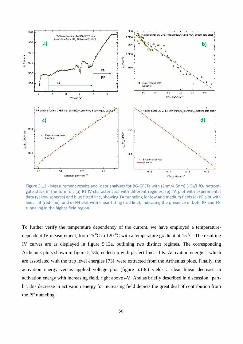
50
To further verify the temperature dependency of the current, we have employed a temperature-
dependent IV measurement, from 25 oC to 120
oC with a temperature gradient of 15
oC. The resulting
IV curves are as displayed in figure 5.13a, outlining two distinct regimes. The corresponding
Arrhenius plots shown in figure 5.13b, ended up with perfect linear fits. Activation energies, which
are associated with the trap level energies [73], were extracted from the Arrhenius plots. Finally, the
activation energy versus applied voltage plot (figure 5.13c) yields a clear linear decrease in
activation energy with increasing field, right above 4V. And as briefly described in discussion “part-
b”, this decrease in activation energy for increasing field depicts the great deal of contribution from
the PF tunneling.
a)
c)
b)
d)
Figure 5.12:- Measurement results and data analyses for BG-GFETs with (2nm/4.5nm) SiO2/HfO2 bottom-gate stack in the form of: (a) RT IV-characteristics with different regimes, (b) TA plot with experimental data (yellow spheres) and blue fitted line, showing TA tunneling for low and medium fields (c) PF plot with linear fit (red line); and d) FN plot with linear fitting (red line), indicating the presence of both PF and FN tunneling in the higher field region.
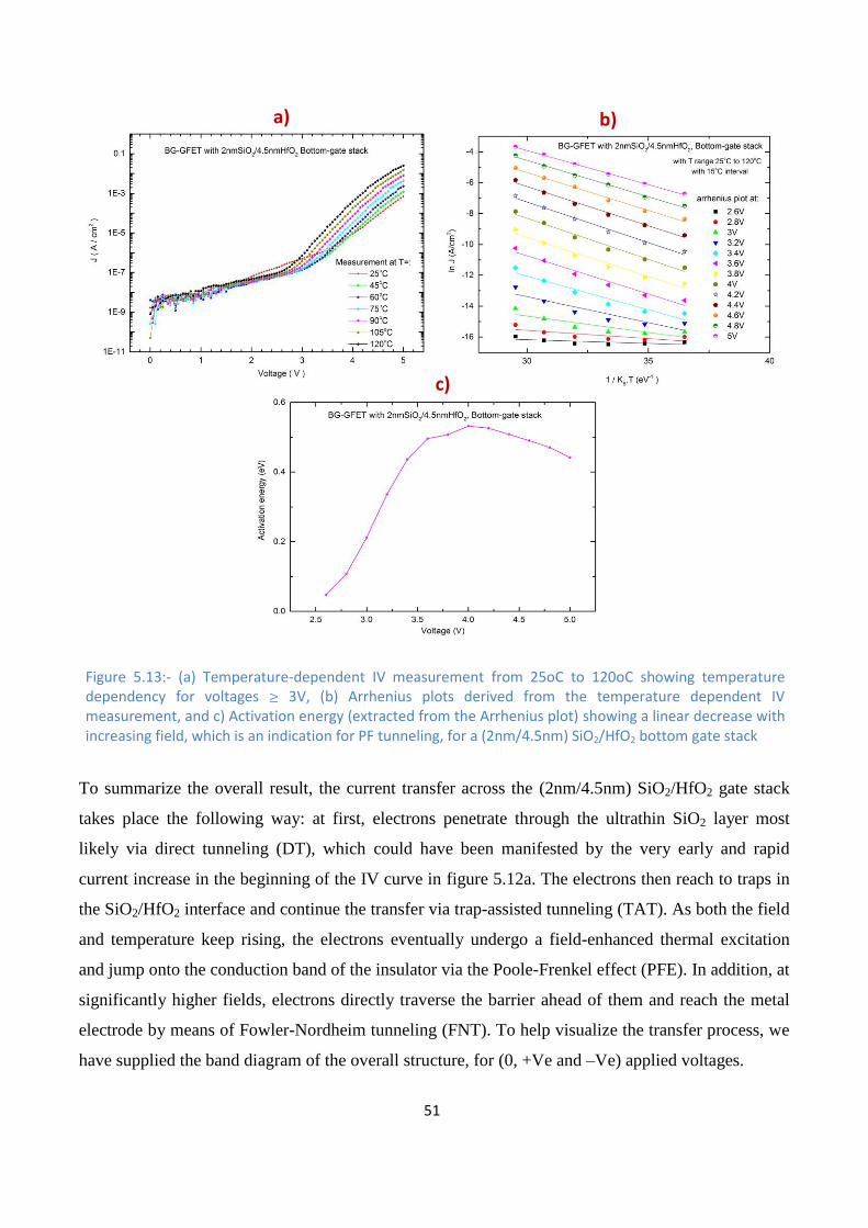
51
To summarize the overall result, the current transfer across the (2nm/4.5nm) SiO2/HfO2 gate stack
takes place the following way: at first, electrons penetrate through the ultrathin SiO2 layer most
likely via direct tunneling (DT), which could have been manifested by the very early and rapid
current increase in the beginning of the IV curve in figure 5.12a. The electrons then reach to traps in
the SiO2/HfO2 interface and continue the transfer via trap-assisted tunneling (TAT). As both the field
and temperature keep rising, the electrons eventually undergo a field-enhanced thermal excitation
and jump onto the conduction band of the insulator via the Poole-Frenkel effect (PFE). In addition, at
significantly higher fields, electrons directly traverse the barrier ahead of them and reach the metal
electrode by means of Fowler-Nordheim tunneling (FNT). To help visualize the transfer process, we
have supplied the band diagram of the overall structure, for (0, +Ve and –Ve) applied voltages.
a) b)
c)
Figure 5.13:- (a) Temperature-dependent IV measurement from 25oC to 120oC showing temperature dependency for voltages 3V, (b) Arrhenius plots derived from the temperature dependent IV measurement, and c) Activation energy (extracted from the Arrhenius plot) showing a linear decrease with increasing field, which is an indication for PF tunneling, for a (2nm/4.5nm) SiO2/HfO2 bottom gate stack

52
e) (2nm/ 4.2nm) SiO2/ “Al2O3+TiO2 mix” bottom-gate stack
The analyses results in here are more or less similar to the ones we had in discussion “part-d” and
obviously, the interpretation will somehow be similar to the ones we did in there. Hence, we
recommend the reader to refer back to discussion “part-d”, for detailed descriptions regarding the
overall current transfer process. To generally highlight the mechanisms taking part in the transfer;
it seems that Fowler-Nordheim in the high field regime and defect-mediated processes both in the
low and high field regimes, contribute to the total current transferred across the gate-stack under
study. Equivalent to the ones given in figure 5.14, here in figure 5.15 are the schematic band
diagrams for the structure we are dealing with. To the best of our knowledge, no values for barrier
height, electron affinity or band offset relative to silicon, have been reported for this new
composition (“Al2O3/TiO2” mix with 1:1 ALD pulse ratio) so far. Hence, its position from the
vacuum level and thereby from the silicon conduction band or SiO2 is just approximation.
”mix
”
Figure 5.15:- Schematic band diagrams of BG-GFET structures with (2nm/≈4.2nm) SiO2/”Al2O3+TiO2 mix” bottom gate stack: (a) band alignment at Zero bias (flat band condition), (b) band diagram showing the device’s operation for +Ve applied voltages and; (c) the band structure at -Ve applied voltages, in which electrons either undergo a step tunneling or traverse across both the whole thickness of both barriers
0.9 eV
4.5eV
SLG
SiO
2
”mix”
Al2O3/TiO2
4.05
eV
n-Si
(a)
SLG
e
n-Si
SiO
2
Al2O3/TiO2 ”mix”
(b)
SiO
2
SLG
n-Si
Al 2
O3/T
iO2
(c)
SiO
2
2 e
V
0.9 eV
4.5eV 2.0 eV
HfO2 n-Si
4.05 eV
(a)
SLG
e
n-Si
SiO
2
HfO2
SLG
(b)
n-Si
SiO
2
SLG
HfO2
(c)
Figure 5.14:- Schematic band diagrams of a BG-GFET with (2nm/4.5nm) SiO2/HfO2 bottom gate stack showing: (a) band alignment at Zero voltage (flat band condition), (b) for +Ve applied voltages and; (c) -Ve applied voltages

53
Apart from the similarities in the current transfer processes and the respective mechanisms they
are attributed to, there exists a slight difference between the case in here and the one in “part-d”.
This slight difference can be stated as follows: in the earlier case, Fowler-Nordheim and Poole-
Frenkel seem to run head-to-head (figures 5.12c & d) and thus it wasn’t easy to tell which
mechanism dominates the current transfer process. Whereas in the current case, by looking at
figures 5.16a, b & c, it is much easier to tell that the majority of the current transfer is being
handled by defect-mediated processes in general term. The temperature dependent measurement
results in figure 5.17 have also approved this fact.
a)
c)
b)
d)
Figure 5.16:- (a) Room temperature IV-characteristics plot, (b) TA plot with experimental data (solid spheres) and black fitted line, indicating TA tunneling in the low field region; (c) PF plot with linear fit (green line), which indicates a dominating PF tunneling both in the low and medium field region; and (d) FN plot with linear fitting (blue line), for BG-GFET structures with (2nm/4.2nm) SiO2/”Al2O3+TiO2 mix” bottom-gate stack
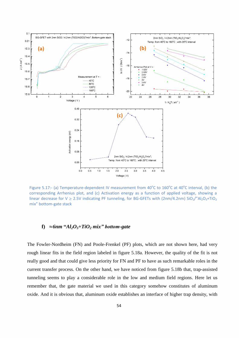
54
f) 6nm “Al2O3+TiO2 mix” bottom-gate
The Fowler-Nordheim (FN) and Poole-Frenkel (PF) plots, which are not shown here, had very
rough linear fits in the field region labeled in figure 5.18a. However, the quality of the fit is not
really good and that could give less priority for FN and PF to have as such remarkable roles in the
current transfer process. On the other hand, we have noticed from figure 5.18b that, trap-assisted
tunneling seems to play a considerable role in the low and medium field regions. Here let us
remember that, the gate material we used in this category somehow constitutes of aluminum
oxide. And it is obvious that, aluminum oxide establishes an interface of higher trap density, with
(a) (b)
(c)
Figure 5.17:- (a) Temperature-dependent IV measurement from 40oC to 160oC at 40oC interval, (b) the corresponding Arrhenius plot, and (c) Activation energy as a function of applied voltage, showing a linear decrease for V 2.5V indicating PF tunneling, for BG-GFETs with (2nm/4.2nm) SiO2/”Al2O3+TiO2 mix” bottom-gate stack

55
silicon [70]. Hence the presence of trap-assisted tunneling for the current transfer through the
barrier under discussion makes so much sense.
We also know that, our gate material contains titanium oxide in equal proportion to aluminum
oxide. And it is true that, the barrier height of titanium oxide is almost about the same level or
slightly below the conduction band of silicon [74]. Thus, Schottky Emission (SE) could be a
possibility, for which we have made analysis on a current measured at 120 oC (figure 5.18c). It
seems that, this IV characteristics plot show three different regimes (RI, RII & RIII), whose
corresponding SE plot appear to have a very good linear fit (figure 5.18d). This could be a path
finder for Schottky emission (SE) and following this clue; we further analyzed our temperature
(a) (b)
(c) (d) at T = 120 oC
Figure 5.18:- (a) IV characteristics at room temperature, (b) Trap-assisted tunneling plot (dark squares = experimental data and Blue line = linear fit), (c) IV characteristics at 120 oC showing three distinct current transfer regimes; and (d) Schottky Emission (SE) plot with three different fitted regions corresponding to the identified regimes in (c); for BG-GFET structures with 6nm “Al2O3/TiO2 mix” bottom gate.

56
dependent IV data, figure 5.19a, measured from 25 oC to 200
oC. As can be seen in the graph, this
plot has clearly delineated three temperature dependency zones, in which the temperature
dependency decreases as one goes from region I to region III, following an increase in the applied
electric field.
The Arrhenius plot in figure 5.19b, which is derived from the temperature-dependent IV result,
shows a clear trend with perfect linear fits. The extracted activation energy attains its maximum
value (0.6 eV) at around 1.25V and afterwards it decreases linearly as the field increases. Here let
us recall the fact that, just like the Poole-Frenkel (PF) effect, Schottky emission (SE) is also
characterized by barrier lowering for high field and temperature. The barrier lowering in turn is
manifested through low activation energy at high field; and that is exactly what one can notice
(b)
(d) (c)
(a)
I
II
III
Figure 5.19:- (a) temperature-dependent current measured from 25 oC to 200 oC, where three distinct regions are outlined. in this graph, there a high temperature dependence at low voltages but the dependency decreases towards higher voltages, (b) Arrhenius plot with good linear fit for 1V, (c) Richardson SE plots with good linear fits for 1V, 1.5V, 1.7V and 2V and the corresponding barrier heights are extracted from these four fittings, and (d) Activation energy Vs Voltage plot. The activation energies were extracted from the perfectly fitted lines.

57
from figure 5.19d. In addition, figure 5.19c contains the Richardson SE plots for different voltage
values and perfect linear fits were obtained for voltages 1V. From the slopes of the fitted lines,
we extracted the barrier heights (ɸB) and the resulting values are in the range from 0.313eV to
0.562eV. As we have mentioned earlier, we have not found any report regarding the band offset
of “Al2O3/TiO2 mix” with respect to silicon, to compare with. Nevertheless, we believe that the
barrier height values we obtained look reasonable that, electrons from the silicon conduction band
can surmount them at high temperatures.
Therefore, based on the ongoing discussions, trap-assisted takes care of the low and medium filed
current transfer at low temperatures; whereas Schottky emission (SE) dominates the high
temperature current transfer across the 6nm “Al2O3+TiO2 mix” bottom-gate. The schematic band
diagrams for the whole structure can be seen below, in figure 5.20.
g) 6.6nm TiO2 bottom-gate
Here, the current transfer properties of a 6.6nm thick TiO2 gate were examined and the results are
presented in figures 5.21 and 5.22. Our analyses results turn out in a way that, trap-assisted
tunneling help out the transfer process at very low fields (the figure is not included here). The FN
and PF plots, which both are not shown here, do not show significant linear trends in respective
field regions. Hence, we believed that neither of them plays an outstanding role to the overall
current transfer process. However, the SE plot [ln(JSE) Vs √ ) at 25 oC shows a considerable
linear trend in reasonable field regions; and that motivated us to check for Schottky emissions
(SE) at higher temperatures.
Figure 5.20:- Schematics of band diagram of BG-GFETS with “Al2O3+TiO2 mix” bottom-gate illustrating: a) the band alignment in flat band condition and b) the band structure for +Ve applied voltage with a Schottky emission of electrons indicated with red broken arrow.
4.05 eV
(a)
”mix”
Al2O3/TiO2
SLG
4.5eV
n-Si
e
n-Si Al2O3/TiO2
”mix”
(b)
SLG

58
Then, to see the effect of temperature on the current transfer across this gate insulator, we
accomplished a temperature-dependent IV measurement from 25 oC to 120
oC with a 15
oC
interval (figure 5.21a). The resulting Arrhenius plots in figure 5.21b have yielded linear trends,
which perfectly fit to straight lines, and this could be an indication that the current transfer process
solely depend on temperature. In addition, the extracted activation energy shows a decreasing
trend after some voltage values and thereby reached minimum at the highest voltage value. As we
have described in the previous discussions, this decrease in activation energy with increasing
voltage could be associated with the barrier lowering at the SiO2/TiO2 interface.
We have also analyzed the current measured at 105 oC, which is part of our temperature-
dependent IV measurement results in figure 5.21a. The inset of figure 5.22a shows this IV plot,
with likely three regimes marked with Green, blue and red horizontal arrows. And shown in figure
5.22a, is the SE plot (ln(JSE) Vs √ ) at 105 oC, showing three linear regions perfectly
associated with the three regimes identified in the IV-characteristics plot. Hence, this is an
indication that, at higher temperatures SE has become the anchor of the current transfer process in
this structure. To strengthen our conclusion, we have made a conventional Richardson’s plot [(ln
(JSE/T2) Vs (1/KBT)], which we have presented in figure 5.22b. These SE plots are perfectly linear
and thus the barrier height ɸB can be extracted from the slopes of the fitted lines [57]. The barrier
height values we extracted are in the range of: 0.262eV to 0.45eV, which is acceptable
(a) (b)
Figure 5.21:- (a) a graph showing the temperature-dependency of current measured from 25 oC to 120 oC. the temperature dependency increases until some voltage values and then starts to diminish as one goes to higher fields; and (b) the corresponding Arrhenius plot for voltages from 1.05 to 3V showing a good linear fit for voltages 1.35V, from which the activation energies are extracted.

59
considering the conduction band offset (CBO) of TiO2 from the conduction band of silicon [74].
Hence, according to our results, the current transfer mechanism in the 6.6nm TiO2 gate oxide is
totally dominated by Schottky emission (SE).
The schematic band diagrams showing the band structures of the device for two cases (0V and
+ve applied voltages) are given in figure 5.23, below.
Figure 5.23:- Schematic band diagrams of BG-GFETS with “Al2O3+TiO2 mix” bottom-gate, showing: a) band alignment in flat band condition; and b) the band structure at low +Ve applied voltages, in which electrons easily overcome the low barrier by means of Schottky Emission (SE)
Figure 5.22:- (a) SE plot for a current measured at 105oC showing straight line fittings (green, blue and red) in three different regimes. The inset shows the IV-characteristics at 105 oC . (b) Richardson SE plots (ln(J/T2) Vs (1/KB.T) with linear fittings, where the perfect fittings indicate the temperature dependence and the barrier height is extracted from this graph.
(a) (b)

60
6. Conclusions and Outlook
Two batches of device fabrication and characterization processes have been carried out. In the
first batch, MOS capacitors with seven different dielectric materials were fabricated and then IV
and CV measurements were done. According to the IV measurement results, TiO2 and SiO2 were
confirmed to be the most and the least-leaky oxides, respectively. On the basis of the first batch
results, four different oxides of similar thicknesses (i.e. 2nm/4.5nm SiO2/HfO2, 2nm/4.2nm SiO2/
“Al2O3+TiO2 mix”, 6nm “Al2O3+TiO2 mix”, and 6.6nm TiO2) and also SiO2 with three different
thicknesses (2nm, 5nm and 10nm) were chosen as gate oxides to build BG-GFET structures.
During the second batch process, different BG-GFETs with the seven gate oxides mentioned
above, were successfully fabricated. IV and temperature-dependent IV measurements were
employed, and the vertical current transfer mechanisms across each gate dielectric were
investigated. In addition comparing results obtained from devices with graphene under and on top
of contacts, most results have confirmed that devices with graphene on top of contacts show
relatively lower current levels and that could lead to a conclusion that there emerges a higher
contact resistance when graphene is on top of the Ti/Au contacts than when it is under.
Based on our analysis results, direct tunneling (DT) was found to be the dominant mechanism in
the 2nm SiO2, while Fowler-Nordheim (FN) tunneling is proved to dominate the transfer
properties of the 10nm SiO2 bottom-gate. Unlike the 2nm and 10nm SiO2, the current transfer
through the 5nm SiO2 was revealed to come from the contribution of two mechanisms (FN and
Poole-Frenkel).
Furthermore, FN appears to collaborate with defect-mediated processes, to deliver the current
across the 2nm/4.5nm SiO2/HfO2 gate stack. Although FN seemed to have a valuable contribution
to the current transfer through the 2nm/4.2nm SiO2/“Al2O3+TiO2 mix” gate stack, defect-
mediated, in particular PF, was observed to be the main mechanism handling the overall transfer
process. The current conduction across the 6nm“Al2O3+TiO2 mix” gate oxide is found to be the
result of Schottky emission (SE) in the high temperature and high field, in cooperation with trap-
assisted tunneling (TAT) acting in the low field region for low temperatures. On the other hand,
SE was suggested as the dominant mechanism in the 6.6nm TiO2 bottom-gate, provided that TAT
also has a little contribution in the low field region at room temperature.

61
The presence of temperature-dependent/ defect mediated processes investigated so far, in general
indicate the existence of interface states and trap cites or defects within the oxides. This basically
would be a drawback when using these tunneling barriers in GBTs, by causing inconsistency and
unreliability of the device performances and could even result in short device life. On the other
hand, SE and FN tunneling are believed to be favorable for GBT applications, for they are
consistent and can secure device reliability. Hence, among the gate oxides whose results are
highlighted above, those in which SE and FN contribute to their current transfer are potential
candidates for a tunneling barrier in GBTs. However, much work needs to be done to suppress the
defect-mediated processes.
We therefore would like to suggest a future work on optimization of heights and thickness of
tunneling barriers. In addition, we highly recommend further work towards improving fabrication
conditions and optimizing the fabrication parameters, for the oxides we have already studied. This
is mainly intended to produce oxides of better quality than the ones we had (i.e. with quite lower
interface states and lower defect densities) and thereby suppress the defect-mediated processes
manifested in our study. Furthermore, we would also like to suggest experimental studies using
some other dielectric materials of reasonable band-offsets with respect to silicon, which could
have feasible potential applications as tunneling barriers for GBTs.

62
7. References
[1] K. S. Novoselov, A. K. Geim, S. V Morozov, D. Jiang, Y. Zhang, S. V Dubonos, I. V
Grigorieva, and A. A. Firsov, “Electric field effect in atomically thin carbon films.,”
Science (New York, N.Y.), vol. 306, no. 5696, pp. 666–9, Oct. 2004.
[2] P. R. Wallace, “The Band Theory of Graphite,” Physical review, vol. 71 No.9, May 1947.
[3] K. I. Bolotin, K. J. Sikes, Z. Jiang, M. Klima, G. Fudenberg, J. Hone, P. Kim, and H. L.
Stormer, “Ultrahigh electron mobility in suspended graphene,” Solid State
Communications, vol. 146, no. 9–10, pp. 351–355, Jun. 2008.
[4] M. C. Lemme, “Current Status of Graphene Transistors,” Solid State Phenomena, vol. 156–
158, pp. 499–509, Oct. 2009.
[5] A. Geim and K. Novoselov, “The rise of graphene,” Nature materials, pp. 183–191, 2007.
[6] W. Mehr, J. Dabrowski, J. C. Scheytt, G. Lippert, Y. Xie, S. Member, M. C. Lemme, M.
Ostling, and G. Lupina, “Vertical Graphene Base Transistor,” vol. 33, no. 5, pp. 691–693,
2012.
[7] M. Freitag, “Nanoelectronics goes flat out,” Nature nanotechnology, vol. 3, pp. 455–457,
Aug. 2008.
[8] A. H. Castro Neto, N. M. R. Peres, K. S. Novoselov, and A. K. Geim, “The electronic
properties of graphene,” Reviews of Modern Physics, vol. 81, no. 1, pp. 109–162, Jan.
2009.
[9] C. Lee, X. Wei, J. W. Kysar, and J. Hone, “Measurement of the elastic properties and
intrinsic strength of monolayer graphene.,” Science (New York, N.Y.), vol. 321, no. 5887,
pp. 385–8, Jul. 2008.
[10] K. S. Novoselov, A. K. Geim, S. V Morozov, D. Jiang, M. I. Katsnelson, I. V Grigorieva,
S. V Dubonos, and A. A. Firsov, “Two-dimensional gas of massless Dirac fermions in
graphene.,” Nature, vol. 438, no. 7065, pp. 197–200, Nov. 2005.
[11] M. S. Purewal, Y. Zhang, and P. Kim, “Unusual transport properties in carbon based
nanoscaled materials: nanotubes and graphene,” Physica Status Solidi (B), vol. 243, no. 13,
pp. 3418–3422, Nov. 2006.
[12] A. S. Mayorov, R. V Gorbachev, S. V Morozov, L. Britnell, R. Jalil, L. a Ponomarenko, P.
Blake, K. S. Novoselov, K. Watanabe, T. Taniguchi, and A. K. Geim, “Micrometer-scale
ballistic transport in encapsulated graphene at room temperature.,” Nano letters, vol. 11,
no. 6, pp. 2396–9, Jun. 2011.
[13] W. K. Tse, E. H. Hwang, and S. Das Sarma, “Ballistic hot electron transport in graphene,”
Applied Physics Letters, vol. 93, no. 2, p. 023128, 2008.

63
[14] C. Berger, Z. Song, X. Li, X. Wu, N. Brown, C. Naud, D. Mayou, T. Li, J. Hass, A. N.
Marchenkov, E. H. Conrad, P. N. First, and W. a de Heer, “Electronic confinement and
coherence in patterned epitaxial graphene.,” Science (New York, N.Y.), vol. 312, no. 5777,
pp. 1191–6, May 2006.
[15] S. Morozov, K. Novoselov, M. Katsnelson, F. Schedin, D. Elias, J. Jaszczak, and A. Geim,
“Giant Intrinsic Carrier Mobilities in Graphene and Its Bilayer,” Physical Review Letters,
vol. 100, no. 1, p. 016602, Jan. 2008.
[16] E. Hwang, S. Adam, and S. Sarma, “Carrier Transport in Two-Dimensional Graphene
Layers,” Physical Review Letters, vol. 98, no. 18, p. 186806, May 2007.
[17] A. A. Balandin, S. Ghosh, W. Bao, I. Calizo, D. Teweldebrhan, F. Miao, and C. N. Lau,
“Superior thermal conductivity of single-layer graphene.,” Nano letters, vol. 8, no. 3, pp.
902–7, Mar. 2008.
[18] P. Blake, P. D. Brimicombe, R. R. Nair, T. J. Booth, D. Jiang, F. Schedin, L. A.
Ponomarenko, S. V Morozov, H. F. Gleeson, E. W. Hill, A. K. Geim, and K. S. Novoselov,
“Graphene-based liquid crystal device.,” Nano letters, vol. 8, no. 6, pp. 1704–8, Jun. 2008.
[19] T. J. Booth, P. Blake, R. R. Nair, D. Jiang, E. W. Hill, U. Bangert, A. Bleloch, M. Gass, K.
S. Novoselov, M. I. Katsnelson, and A. K. Geim, “Macroscopic graphene membranes and
their extraordinary stiffness.,” Nano letters, vol. 8, no. 8, pp. 2442–6, Aug. 2008.
[20] P. Avouris, “Fast graphene-based electronics and optoelectronics,” 10th IEEE International
Conference on Nanotechnology, pp. 6–9, Aug. 2010.
[21] F. Schwierz, “Graphene transistors” Nature nanotechnology, vol. 5, no. 7, pp. 487–96, Jul.
2010.
[22] M. Han, B. Özyilmaz, Y. Zhang, and P. Kim, “Energy Band-Gap Engineering of Graphene
Nanoribbons,” Physical Review Letters, vol. 98, no. 20, p. 206805, May 2007.
[23] X. Li, X. Wang, L. Zhang, S. Lee, and H. Dai, “Chemically derived, ultrasmooth graphene
nanoribbon semiconductors.,” Science (New York, N.Y.), vol. 319, no. 5867, pp. 1229–32,
Feb. 2008.
[24] R. Quhe, J. Zheng, G. Luo, Q. Liu, R. Qin, J. Zhou, D. Yu, S. Nagase, W.-N. Mei, Z. Gao,
and J. Lu, “Tunable and sizable band gap of single-layer graphene sandwiched between
hexagonal boron nitride,” NPG Asia Materials, vol. 4, no. 2, p. e6, Feb. 2012.
[25] D. Nezich and T. Palacios, “Graphene Frequency Multipliers,” IEEE Electron Device
Letters, vol. 30, no. 5, pp. 547–549, May 2009.
[26] H. Wang, A. Hsu, and J. Wu, “Graphene-based ambipolar RF mixers,” Electron Device
Letters, vol. 31, no. 9, pp. 906–908, 2010.
[27] F. Bonaccorso, Z. Sun, T. Hasan, and A. C. Ferrari, “Graphene photonics and
optoelectronics,” Nature Photonics, vol. 4, no. 9, pp. 611–622, Aug. 2010.

64
[28] X. Miao, S. Tongay, M. K. Petterson, K. Berke, A. G. Rinzler, B. R. Appleton, and A. F.
Hebard, “High efficiency graphene solar cells by chemical doping.,” Nano letters, vol. 12,
no. 6, pp. 2745–50, Jun. 2012.
[29] P. Avouris, “Graphene: Electronic and Photonic Properties and Devices.,” Nano letters, pp.
4285–4294, Sep. 2010.
[30] F. Xia, T. Mueller, Y.-M. Lin, A. Valdes-Garcia, and P. Avouris, “Ultrafast graphene
photodetector.,” Nature nanotechnology, vol. 4, no. 12, pp. 839–43, Dec. 2009.
[31] A. K. Geim, “Graphene: status and prospects.,” Science (New York, N.Y.), vol. 324, no.
5934, pp. 1530–4, Jun. 2009.
[32] Y. Wang, R. Yang, Z. Shi, L. Zhang, D. Shi, E. Wang, and G. Zhang, “Super-elastic
graphene ripples for flexible strain sensors.,” ACS nano, vol. 5, no. 5, pp. 3645–50, May
2011.
[33] J. T. Robinson, F. K. Perkins, E. S. Snow, Z. Wei, and P. E. Sheehan, “Reduced graphene
oxide molecular sensors.,” Nano letters, vol. 8, no. 10, pp. 3137–40, Oct. 2008.
[34] J. S. Bunch, A. M. van der Zande, S. S. Verbridge, I. W. Frank, D. M. Tanenbaum, J. M.
Parpia, H. G. Craighead, and P. L. McEuen, “Electromechanical resonators from graphene
sheets.,” Science (New York, N.Y.), vol. 315, no. 5811, pp. 490–3, Jan. 2007.
[35] Dale. A. C. Brownson, D. K. Kampouris, and C. E. Banks, “An overview of graphene in
energy production and storage applications,” Journal of Power Sources, vol. 196, no. 11,
pp. 4873–4885, Jun. 2011.
[36] C. Soldano, A. Mahmood, and E. Dujardin, “Production, properties and potential of
graphene” ScienceDirect, Carbon, vol. 48, p. 21, 2010.
[37] G. Nanoelectronics, C. Berger, Z. Song, T. Li, X. Li, A. Y. Ogbazghi, R. Feng, Z. Dai, A.
N. Marchenkov, E. H. Conrad, P. N. First, and W. A. De Heer, “Ultrathin Epitaxial
Graphite : 2D Electron Gas Properties and a Route toward,” J.Phys. Chem. pp. 19912–
19916, 2004.
[38] W. A. de Heer and C. Berger, “Epitaxial graphene,” Journal of Physics D: Applied Physics,
vol. 45, no. 15, p. 150301, Apr. 2012.
[39] A. Reina, X. Jia, J. Ho, D. Nezich, H. Son, V. Bulovic, M. S. Dresselhaus, and J. Kong,
“Large area, few-layer graphene films on arbitrary substrates by chemical vapor
deposition.,” Nano letters, vol. 9, no. 1, pp. 30–5, Jan. 2009.
[40] H. J. Park, J. Meyer, S. Roth, and V. Skákalová, “Growth and properties of few-layer
graphene prepared by chemical vapor deposition,” ScienceDirect, Carbon, vol. 48, no. 4,
pp. 1088–1094, Apr. 2010.

65
[41] K. S. Kim, Y. Zhao, H. Jang, S. Y. Lee, J. M. Kim, K. S. Kim, J.-H. Ahn, P. Kim, J.-Y.
Choi, and B. H. Hong, “Large-scale pattern growth of graphene films for stretchable
transparent electrodes.,” Nature, vol. 457, no. 7230, pp. 706–10, Feb. 2009.
[42] S. Park and R. S. Ruoff, “Chemical methods for the production of graphenes.,” Nature
nanotechnology, vol. 4, no. 4, pp. 217–24, Apr. 2009.
[43] C. Zeng, E. B. Song, M. Wang, S. Lee, C. M. Torres, J. Tang, B. H. Weiller, and K. L.
Wang, “Vertical graphene-base hot-electron transistor.,” Nano letters, vol. 13, no. 6, pp.
2370–5, Jun. 2013.
[44] S. Vaziri, G. Lupina, C. Henkel, A. Smith, M.Östling, J.Dabrowski, G.Lippert, W.Mehr
and M. C. Lemme, “A Graphene-Based Hot Electron Transistor,” Nano letters, 2013.
[45] L. Britnell, R. V Gorbachev, R. Jalil, B. D. Belle, F. Schedin, a Mishchenko, T. Georgiou,
M. I. Katsnelson, L. Eaves, S. V Morozov, N. M. R. Peres, J. Leist, A. K. Geim, K. S.
Novoselov, and L. A. Ponomarenko, “Field-effect tunneling transistor based on vertical
graphene heterostructures.,” Science (New York, N.Y.), vol. 335, no. 6071, pp. 947–50, Feb.
2012.
[46] F. Driussi, P. Palestri, and L. Selmi, “Modeling, simulation and design of the vertical
Graphene Base Transistor,” Microelectronic Engineering, vol. 109, pp. 338–341, Sep.
2013.
[47] Y. Taur, S. Member, D. A. Buchanan, W. E. I. Chen, D. J. Frank, K. E. Ismail, S. Lo, G. A.
Sai-halasz, R. G. Viswanathan, H. C. Wann, S. J. Wind, and H. Wong, “CMOS Scaling
into the Nanometer Regime,” Proceedings of the IEEE, vol. 85, no. 4, 1997.
[48] C. A. Mead, “Operation of Tunnel-Emission Devices,” Journal of Applied Physics, vol. 32,
no. 4, p. 646, 1961.
[49] W. Soutter, “An Introduction to Quantum Tunneling” pp. 1–5, 1927.
[50] K. Roy, S. Mukhopadhyay, and H. Mahmoodi-Meimand, “Leakage Current Mechanisms
and Leakage Reduction Techniques in Deep-Submicrometer CMOS Circuits,” Proceedings
of the IEEE, vol. 91, no. 2, 2003.
[51] R. W. Dutton, “Direct tunneling current model for circuit simulation,” International
Electron Devices Meeting 1999. Technical Digest (Cat. No.99CH36318), no. 3, pp. 735–
738.
[52] R . H . Fowler and L . Nordheim, “Electron Emission in Intense Electric Fields”
Proceedings of the Royal Society of London . Series A , Containing Papers of a
Mathematical and Physical character, Published by : The Royal Society Stable URL :
http://www.jstor.org/stable/95,” vol. 119, no. 781, pp. 173–181, May 1, 1928.
[53] M. A. Grado-Caffaro and M. Grado-Caffaro, “Fowler–Nordheim electron tunneling under
very intense electric field,” Optik - International Journal for Light and Electron Optics,
vol. 121, no. 21, pp. 2001–2002, Nov. 2010.

66
[54] E. Miranda and F. Palumbo, “Analytic expression for the Fowler–Nordheim V–I
characteristic including the series resistance effect,” Solid-State Electronics, vol. 61, no. 1,
pp. 93–95, Jul. 2011.
[55] W. Reimann, Arnold L. “thermioic emission”, London: Chapman & Hall Ltd, Henrietta
Street, W.C.2, 1934, pp. 1–4.
[56] S. R. Pollack, “Schottky Field Emission Through Insulating Layers,” Journal of Applied
Physics, vol. 34, no. 4, p. 877, 1963.
[57] Z. H. Liu, G. I. Ng, S. Arulkumaran, Y. K. T. Maung, and H. Zhou, “Temperature-
dependent forward gate current transport in atomic-layer-deposited Al[sub 2]O[sub
3]/AlGaN/GaN metal-insulator-semiconductor high electron mobility transistor,” Applied
Physics Letters, vol. 98, no. 16, p. 163501, 2011.
[58] B. Ricc, G. Gozzi, and M. Lanzoni, “Modeling and Simulation of Stress-Induced Leakage
Current in Ultrathin SiO Films,” IEEE transactions on electron devices, vol. 45, no. 7, pp.
1554–1560, 1998.
[59] R. M. and C. Hut, “Stress-Insuced Current in Thin Silicon Dioxide,” Advanced Products
Research and Development Laboratory Motorola, Inc., MD K10, 3501 Ed Bluestein Blvd..
Austin, Texas 78721 U.S.A. f Department of Electrical Engineering and Computer Sciences
University of California, Berkeley, CA 94720 U.S.A., vol. IEEE, no. c, pp. 139–142, 1992.
[60] S. Ganichev, E. Ziemann, W. Prettl, I. Yassievich, A. Istratov, and E. Weber, “Distinction
between the Poole-Frenkel and tunneling models of electric-field-stimulated carrier
emission from deep levels in semiconductors,” Physical Review B, vol. 61, no. 15, pp.
10361–10365, Apr. 2000.
[61] P. V. Aleskandrova, V. K. Gueorguiev, T. E. Ivanov, and J. B. Koprinarova, “Poole-
Frenkel conduction in Al/ZrO2 /SiO 2 /Si structures,” The European Physical Journal B,
vol. 52, no. 4, pp. 453–457, Aug. 2006.
[62] D. S. Jeong and C. S. Hwang, “Tunneling-assisted Poole-Frenkel conduction mechanism in
HfO[sub 2] thin films,” Journal of Applied Physics, vol. 98, no. 11, p. 113701, 2005.
[63] H. Sio, S. Mos, G. Stacks, R. G. S. Iii, J. Reed, C. Buu, H. Bui, R. Butler, G. Bersuker, and
W. B. Knowlton, “Temperature (5.6-300K) Dependence Comparison of Carrier Transport
Mechanisms in HfO2/SiO2 and SiO2 MOS Gate Stacks,” IEEE, vol. 02, pp. 48–54, 2008.
[64] Online resource, “Quantum Mechanical Tunneling,” pp. 1–12. Access date: 2013-07-07,
9:00PM, link: http://www.iue.tuwien.ac.at/phd/entner/node23.html.
[65] B. L. Yang, P. T. Lai, and H. Wong, “Conduction mechanisms in MOS gate dielectric
films,” Microelectronics Reliability, vol. 44, no. 5, pp. 709–718, May 2004.
[66] M. Meuris, S. Arnauts, I. Cornelissen, K. Kenis, M. Lux, S. Degendt, P. M. Teerlinck, R.
Vas, L. Loewensteine, and M. M. Heyns, “Implementation of the IMEC-Clean in advanced
CMOS manufacturing”, IEEE, pp. 3–6, 1993.
67
[67] R. L. Puurunen, “Surface chemistry of atomic layer deposition: A case study for the
trimethylaluminum/water process,” Journal of Applied Physics, vol. 97, no. 12, p. 121301,
2005.
[68] A. H. Taghaboni and P. M. Östling, “Characterization of Tunneling Currents in Graphene
Base Transistors Examiner,” KTH, pp. 1–47, March 2013.
[69] S. Vaziri, “Fabrication and Characterization of Graphene Field Effect Transistors,”, KTH-
The Royal Institute of Technology, 2011.
[70] D. K. Schroder, “Semiconductor Material and Device Characterization”, 3rd ed. New
Jersey: IEEE Press; John Wiley & Sons, Inc., Hoboken, New Jersey, 2006.
[71] S. Xu and Q. Zhang, “Causes of asymmetry in graphene transfer characteristics,” 2010
International Workshop on Junction Technology Extended Abstracts, pp. 1–3, May 2010.
[72] M. Lemme and T. Echtermeyer, M. Baus and H.Kurz, “A graphene field-effect device,”
IEEE Electron Device Letters, vol. 28, no. 4, pp. 282–284, 2007.
[73] A. Alnuaimi, A. Nayfeh, and V. Koldyaev, “Electric-field and temperature dependence of
the activation energy associated with gate induced drain leakage,” Journal of Applied
Physics, vol. 113, no. 4, p. 044513, 2013.
[74] M. Perego, G. Seguini, G. Scarel, M. Fanciulli, and F. Wallrapp, “Energy band alignment
at TiO[sub 2]∕Si interface with various interlayers,” Journal of Applied Physics, vol. 103,
no. 4, p. 043509, 2008.
[75] J. Güttinger, F. Molitor, C. Stampfer, S. Schnez, a Jacobsen, S. Dröscher, T. Ihn, and K.
Ensslin, “Transport through graphene quantum dots.,” Reports on progress in physics.
Physical Society (Great Britain), vol. 75, no. 12, p. 126502, Dec. 2012.
[76] S. Vaziri, G. Lupina, A. Paussa, A. D. Smith, C. Henkel, G. Lippert, J. Dabrowski, W.
Mehr, M. Östling, and M. C. Lemme,“A manufacturable process integration approach for
graphene devices”, Solid-State Electronics, 2013.

www.kth.se
TRITA-ICT-EX-2013:238


![Transition metal oxides/hydroxides nanoarrays for aqueous ......2014/12/08 · Commonly chemical vapor deposition (CVD) [41] is used for controllable fabrication of highly ordered](https://img.pdfslide.us/doc/110x75/60820092bc9b25274e2722bd/transition-metal-oxideshydroxides-nanoarrays-for-aqueous-20141208-.jpg)