Embed Size (px)
Citation preview

FABRICATION AND CHARACTERIZATION OF MICROLASERS
BY THE SOL-GEL METHOD
Thesis by
Lan Yang
In Partial Fulfillment of the Requirements for the
Degree of
Doctor of Philosophy
CALIFORNIA INSTITUTE OF TECHNOLOGY
Pasadena, California
2005
(Defended May 16, 2005)

ii
© 2005
Lan Yang
All Rights Reserved

iii

ivACKNOWLEDGEMENTS
The time I have spent at Caltech was certainly fruitful and enjoyable. Caltech not only
opened the door to scientific research, but also broadened my view in many aspects to the
world. I feel very grateful to spend part of my life in this wonderful place.
There are many people to thank for their support and encouragement, without whom this
thesis would have not been possible. First I would like to thank my thesis advisor,
Professor Kerry J. Vahala, for his patience, support, and guidance through my five years in
his group at Caltech. It has been a great pleasure to be one of his students. His deep
understanding of physics and his fascination with both fundamental and applied science are
what have inspired me most. While allowing and encouraging me to work independently,
he was always ready to offer helpful suggestions and insightful comments. In spite of his
many responsibilities, he was never too busy to give inspiration, detailed comments,
including correcting my naïve grammar mistakes on my papers, or simply to chat. I truly
believe I could not have had a better advisor, and his attitude toward science, education and
even life will serve as a role model for me in the years to come.
I want to thank other members of my thesis Advisory Committee: Professor Demetri
Psaltis, Professor Oskar Painter, Professor David Rutledge and Professor Changhuei Yang,
for their useful comments and suggestions for the work included in this thesis.
I have enjoyed working with people in the lab and would like to thank, Dr. Min Cai, Dr.
Mark Brongersma, Dr. Sean M. Spillane, Dr. Tobias, J. Kippenberg, Hosein Rohksari,
Deniz Armani, and Andrea Martin. Special thanks go to Dr. Tal Carmon and Bumki Min,

vwith whom I have had a fruitful collaboration. I would like to thank Bumki Min for his
willingness to share his knowledge with me and I have enjoyed talking with him very
much. It is also an enjoyable experience working with Dr. Tal Carmon and I like his
“Hebrew wisdom” very much. I also would like to thank Alireza Ghaffari for showing me
how to use some facilities, such as mask aligner and spinner, in the clean room.
I also want to thank my friends for making the graduate school life a colorful experience.
Many thanks go to Lili Yang, Pin Wang, Weiwei Zhong, Yin Gong, Chunhui Mo, Qiang
Yang, Zhengrong Wang, Jiao Lin, Jian Wu, Qingsong Zhang, Wei Liang, Yanyi Huang, Jie
Yu, Ying Li, Charles Fan, Fang Wang, and Chunhua Qi……
I thank my beloved family whose love and encouragement are extremely important to
me. I appreciate what they have done for me throughout these years. I also thank my
husband Hongyu for his unlimited support, who made the possibly-dreary graduate school
life a pleasant experience overall. With beloved ones around, I can move forward full of
passion and hope.

vi

viiABSTRACT
The present study explores the application of new materials systems for low threshold
microlasers, and characterization of the microcavities. The sol-gel method is used for gain
functionalization of high-Q microcavities. A detailed procedure for preparation of the sol-
gel films by the spin-on or dip-coating method is presented. The effect of different process
conditions on the properties and microstructure of the thin films is investigated through
Fourier Transform Infrared (FTIR) Spectroscopy, Scanning Electron Microscopy (SEM),
and etching rate test.
Surface gain functionalization of microsphere cavities is fabricated by coating the
microsphere with a thin layer of Er3+-doped sol-gel films. The optical gain is due to the
population inversion of rare earth ions in the sol-gel films. A fiber taper is used to both
couple the pump power into and extract the laser power out of the microsphere laser. The
laser dynamics change between continuous-wave and pulsating operation by varying the
doping concentration and the thickness of the sol-gel films outside the microsphere.
Surface functionalization is also achieved on the microtoroid on a single silicon chip,
which can be fabricated in parallel using wafer-scale processing and has characteristics that
are more easily controlled than microsphere. The microtoroid can be selectively coated
only at the periphery by making use of the variation of etching rate (in buffered HF) of sol-
gel films with different degrees of densification. The laser performance of the gain
functionalized microtoroids is investigated. Highly confined whispering gallery modes
make possible single-mode microlasers. This work also shows that the high Q microtoroid
laser has a linewidth much lower than 300 kHz.

viii The thesis explores fabrication of high Q microcavities directly from the sol-gel silica
films deposited on a single silicon wafer. Quality factor as high as 2.5 × 10⁷ at 1561 nm is
obtained in toroidal microcavities formed of silica sol-gel, which allows Raman lasing at
absorbed pump power below 1 mW. Additionally, Er3+-doped microlasers are fabricated
from Er3+-doped sol-gel layers with control of the laser dynamics possible by varying the
erbium concentration of the starting sol-gel material. Continuous lasing with a record
threshold of 660 nW for erbium-doped microlaser on a silicon wafer is also obtained.
Analytic formulas are derived to predict the laser performance, such as the laser output
power, the threshold power, and the differential quantum efficiency, under different loading
condition, i.e. the air gap between the fiber-taper coupler and the cavities. The effect of Er3+
concentration on the minimum threshold is also investigated. In addition, we present a
theoretical model in which we include paired ions as the saturable absorber. It shows that
self-pulsing operation can be expected with paired-ions-induced quenching in the system.
The pulsation frequency increases linearly with the square root of the pumping level, which
is consistent with the experimental observation.

ixTABLE OF CONTENTS
Acknowledgements ........................................................................................... iv
Abstract.............................................................................................................vii
Table of Contents .............................................................................................. ix
List of Figures..................................................................................................xiv
List of Tables .................................................................................................xviii
Chapter I: Introduction .................................................................................... 1
1.1 Motivation ........................................................................................ 2
1.2 Organization of the Thesis ............................................................... 3
Chapter II: Whispering gallery type microresonators ................................. 7
2.1. Introduction .................................................................................... 7
2.2. Microsphere resonators .................................................................. 8
2.3 Cavity quality factor (Q) .............................................................. 17
Chapter III: Optical coupling between fiber taper and WGM cavity ...... 23

x 3.1 Introduction .................................................................................. 23
3.2 General methods for coupling to microsphere microcavities ..... 23
3.3 Fabrication of the fiber taper........................................................ 25
3.4 Characterization of the fiber taper modes.................................... 26
3.5 Coupling between the fiber taper and the cavity ......................... 26
3.6 Phase matching between the microcavities and the fiber-taper
coupler............................................................. …...…...…...…...33
3.7 Conclusion …..............................................................................34
Chapter IV: Optical materials by sol-gel process........................................ 35
4.1 Introduction ................................................................................. 35
4.2 An overview of sol-gel process steps ......................................... 35
4.2.1 Hydrolysis and condensation ............................................ 37
4.2.2 Gelation ............................................................................. 38
4.2.3 Ageing ............................................................................... 39
4.2.4 Drying ................................................................................ 39
4.2.5 Densification ..................................................................... 39
4.2.6 Advantages and limitations of sol-gel method ................. 40
4.3 Fabrication of sol-gel films for photonic application................. 41
4.4 Characterization of sol-gel silica film with Fourier Transform
Infrared Spectrometer (FTIR) ..................................................... 42
4.5 Effect of anneal temperature on etching rate of sol-gel film in
buffered Fluoride acid (HF) ........................................................ 44

xi 4.6 Conclusion..................................................................................... 45
Chapter V: Surface functionalization of silica microsphere resonators... 46
5.1 Introduction ................................................................................... 46
5.2 Erbium doped silica glass.............................................................. 46
5.2.1 Er3+-Er3+ interactions............................................................ 48
5.3 Fabrication of silica microsphere.................................................. 49
5.4 Surface functionalization of microsphere..................................... 52
5.5 Coupling between fiber taper and microsphere............................ 54
5.6 Laser performance......................................................................... 56
5.7 Effect of doping thickness on the laser dynamics ........................ 59
5.8 Conclusion..................................................................................... 61
Chapter VI: Surface functionalization of silica microtoroid resonators on
a si chip........................................................................................................ 62
6.1 Introduction .................................................................................. 62
6.2 Characterization of Microtoroid cavities ..................................... 63
6.3 Surface functionalization of microtoroid cavities on a Si chip... 66
6.4 Fiber taper coupled microtoroid lasers on a Si chip.................... 67
6.5 Conclusions .................................................................................. 72
Chapter VII: Fabrication and characterization of microtoroid lasers on a
Si chip ........................................................................................ 73

xii 7.1 Introduction .................................................................................. 73
7.2 Fabrication and characterization of microdisk and microtoroid
cavities from the sol-gel films...................................................... 75
7.2.1 Fabrication of sol-gel films on a silicon wafer.................... 75
7.2.2 Fabrication of microdisk and microtoroid cavities from the
sol-gel films ......................................................................... 76
7.2.3 Characterization of microdisks and microtoroids with
optical microscope and SEM ............................................... 79
7.3 Raman Microlasers from sol-gel films on a Si chip.................... 81
7.4 Er3+-doped Microlasers from sol-gel films on a Si chip ............. 82
7.5 Analysis of Er3+-doped microlasers ............................................. 87
7.5.1 Transmission spectrum of the pump................................ 89
7.5.2 Laser output power of the microlasers ............................ 91
7.5.3 Threshold power of the microlasers ................................ 95
7.5.4 Differential quantum efficiency of the microlasers....... 100
7.5.5 Experimental Results ..................................................... 102
7.6 Conclusions ............................................................................... 105
Chapter VIII: Paired ions induced self-pulsing in Erbium-doped
Microtoroid lasers.................................................................................... 107
8.1 Introduction .............................................................................. 107
8.2 Model for ion pairs inducing self-pulsing ............................... 108
8.3 Experimental results on self-pulsing operation ....................... 116

xiii 8.4 Conclusions ............................................................................... 120
Chapter IX: Conclusion and future work .................................................. 121
Bibliography ................................................................................................... 126
xivLIST OF FIGURES
2.1. The field profile of a TE mode of a microsphere. ..................................... 12
2.2 The field profile of a TE mode of a microsphere,
4-lm and 192,l ,1n === .................................................................. 14
2.3 Images of the WGMs in the taper-sphere coupling zone: (a) l-m=0.
(b) l-m=1. and (c) l-m=5. ............................................................................ 15
2.4 High resolution whispering gallery mode spectrum.................................. 19
3.1 Different coupling scheme for microspheres............................................. 24
3.2 Optical image of waist of the fiber taper. Inset: a standard 125 µm single
mode optical fibers……………………………………………………….25
3.3 Schematic of coupling between fiber taper and cavity.............................. 27
3.4 Different coupling regimes for a cavity with the intrinsic quality factor Qo
of 1×10⁸......................................................................................................... 31
3.5 Normalized transmission of a fiber taper coupled microsphere versus
the air gap between the microsphere and the taper..................................... 33
4.1 Schematic of fabrication of sol-gel films on a substrate ........................... 41
4.2 FTIR spectra of thermal silica and sol-gel silica samples prepared with
different heat treatment................................................................................ 43
5.1 Schematic representation of the Er3+ intra 4f Energy level ........................ 47
5.2 Illustration of fabrication of the microsphere for a silica fiber ................. 50
5.3 Transmission spectrum of a fiber taper coupled microsphere.................... 51
xv
5.4 Schematic of surface functionalization of silica microsphere................... 53
5.5 Schematic of a thin film coated microsphere laser coupled with a fiber
taper............................................................................................................. 55
5.6 Image of the WGMs in the taper-sphere coupling zone........................... 56
5.7 Emission spectrum of a microsphere laser ............................................... 57
5.8 Laser output power versus absorbed pump power in the microsphere
laser .............................................................................................................. 58
5.9 Measured pulsation frequency versus the square root of the laser
output power P ............................................................................................ 60
6.1 Optical micrograph top view of a microtoroid shoing principal and minor
diameters of the toroid ............................................................................... 63
6.2 Simulation of fundamental TM modes for toroid with minor diameters of
(a) 4 µm; (b) 8 µm and (c) 16 µm. ........................................................... 64
6.3 Field intensity distribution along the polar direction for different micro-
toroids........................................................................................................... 65
6.4 Schematic of surface functionalization of a microtoroid on a silicon
chip............................................................................................................. 66
6.5 Illustration showing a micro-chip laser consisting of an Erbium-doped
sol-gel thin film applied to a microtoroid .................................................. 68
6.6 Photomicrograph top view of an Erbium microtoroid laser coupled
by a fiber taper ............................................................................................ 68

xvi6.7 Emission spectrum of a microtoroid laser with approximate diameter
of 80 µm....................................................................................................... 69
6.8 Laser emission spectrum from Er-doped sol-gel thin-film coated
microtoroid laser. ......................................................................................... 70
6.9 Measured laser output power plotted versus absorbed pump power
for a microtoroid laser with a diameter of 80 µm...................................... 71
7.1 Schematic process flow for creation of solgel microcavities on a
Si wafer ....................................................................................................... 77
7.2 Transmission spectrum of a fiber taper coupled microdisk with
diameter of 100 micron .............................................................................. 78
7.3 Optical photomicrograph of (a) circular pads on silicon wafer
(b) under-etched silica disk (c) Microtoroid after CO2 laser reflow .......... 80
7.4 SEM images of microdisks and microtoroids............................................. 81
7.5 Raman emission spectrum of an undoped microtoroid with principal
diameter of 49 µm........................................................................................ 83
7.6 Photomicrograph view (horizontal and vertical) of an Er3+-doped
solgel silica microtoroid laser...................................................................... 85
7.7 Typical laser spectrum of an Er-doped solgel silica microtoroid laser..... 86
7.8 Normalized transmission of pump power as a function of air
gap between the fiber taper coupler and the microlaser ............................. 90
7.9 Laser output power as a function of air gap between the fiber
taper coupler and the microlasers with different intrinsic Q .................... 95

xvii7.10 Threshold pump power as a function of air gap ....................................... 98
7.11 Threshold pump power as a function of erbium concentration in the
microlasers with different intrinsic Q ...................................................... 99
7.12 Quantum efficiency as a function of air gap with different intrinsic Q .102
7.13 Normalized laser output power as a function of air gap......................... 103
7.14 Differential quantum efficiency as a function of air gap........................ 103
7.15 Measured laser output power plotted versus the absorbed pump
power for a microtoroid laser ................................................................. 104
8.1. Cross-relaxation process between paired ions ......................................... 110
8.2 Energy level diagram in current model for paired ions ........................... 112
8.3 Numerical simulation of photon density as a function of time at
different pumping level ............................................................................ 115
8.4 Numerical simulation of evolution of the self-pulsing frequency as
a function of square root of P/Pth............................................................. 116
8.5 Self-pulsing operation of an Er3+-doped microtoroid laser with laser
output power .............................................................................................. 119
8.6 Evolution of the self-pulsing frequency as a function of square root
of the laser output power ........................................................................... 119

xviiiLIST OF TABLES
8.1 Values of parameters used in simulation. .................................................... 117

xix

1C h a p t e r 1
INTRODUCTION
There has been interest in microresonators, which are attractive systems both for
fundamental physics research in the fields of nonlinear optics, cavity quantum
electrodynamics and for applications in sensor for bio-molecule and low threshold
microlasers etc. [1-4]. My research interest lies in exploring application of new materials
system for low threshold microlasers and evaluating the performance of the devices.
Optical gain can be obtained not only through nonlinear optical process such as Stimulated
Raman Scattering (SRS), but also through population inversion of rare earth ions in a host
medium [5]. High finesse microcavities are good candidate for low threshold microlasers.
Chang’s research group reported lasing from rhodamine doped ethanol [6]. Later Campillo
and his colleagues observed Stimulated Raman Scattering from CS2 microdroplets [7-9].
However the liquid droplets are difficult to handle and suffer from their short lifetime due
to the evaporation in the air. More recently, Ilchenko first showed a surface-tension-
induced silica microsphere exhibiting relatively small mode volume with the highest
observed quality factor (Q) up to 1010 at 633 nm corresponding to photon storage times in
the order of microsecond [10]. Subsequently, an ultra-low-threshold microsphere Raman
laser was demonstrated due to high power build-up factor of these ultra-high-Q
microcavities [11]. Nd3+-doped silica microsphere and Er3+-doped phosphate sphere
microlasers have been reported by Sandoghdar and Cai [3, 12], who made the sphere by

2heat-fusing the tip of a doped silica or phosphate wire. All the microspheres are made by
heat-fusing the tip of a glass wire. For the pure silica microsphere, a regular silica optical
fiber can be used, while for the doped microsphere, either the Nd3+-doped silica wire was
obtained by HF etching the cladding of a fiber with a core of 20 µm in diameter doped with
0.2 wt% Nd3+, or the Er3+/Yb3+ codoped phosphate wire was pulled from a piece of melted
Er3+/Yb3+ bulk phosphate glass. However, it tends to form some crystallized spots during
the melting-and-pulling process to get the doped-phosphate wire and further heating can
not get rid of the crystallization defect, which makes the final microsphere inhomogeneous
and degrade the quality factor of the microcavites.
On the other hand, sol-gel method has been used for preparation of oxide in a variety
forms [13]. This thesis centers on the fabrication of microlasers by surface gain
functionalization of existing high-Q microcavities with sol-gel films or directly processing
of sol-gel films into a microlasers. Throughout the thesis work, a CO2 laser was used to
modify the sol-gel materials. The laser reflow process endows the sol-gel material very
high optical quality. This thesis also includes a detailed study of the microlasers. Before
turning to the outline of the thesis, a brief introduction of the sol-gel method in optics field
will be outlined.
1.1 Motivation
The sol-gel process actually offers unique opportunity for the synthesis of optical materials
with composition stoichiometrically controlled. The homogeneous mixture of several

3components in liquid state makes it possible to vary the optical materials over a wide
range of compositions at molecular level, therefore the optical properties of the materials
are tailored, such as Ge dopants to change the refractive index [14], P dopants to increase
nonlinear gain coefficient of silica and rare earth dopants to create gain in the host materials
[15-17]. In summary, the sol-gel method provides an efficient and cost-effective platform
for us to explore the effects of different dopants on the properties of the microcavities.
1.2 Organization of the Thesis
To provide a common footing for the chapters that follow, chapter 2 introduces the origin
of the Whispering Gallery Mode (WGM) cavities. Several terminologies, such as finesse
and optical quality factor, used in cavities are also introduced. The mode characterization
and field distribution of the microsphere is discussed. Tracing of the modes in microsphere
is visible by using up-conversion (540 nm transition) of Er3+ inside the sol-gel films coated
outside the microsphere.
Chapter 3 describes the fabrication process of fiber taper and gives a review of the fiber
taper coupling schemes used throughout this work. A simple theoretical model is presented
to study the coupling mechanism between the fiber taper and the microcavities. The
coupling efficiency adjusted by variation of the air gap between the microcavities and the
taper is discussed in details.

4 Chapter 4 introduces the sol-gel method and its application in optics field. A detailed
procedure for preparation of sol-gel films by spin-on or dip-coating method is presented.
The effect of different annealing temperature on the properties of the thin films is
investigated by Fourier Transform Infrared (FTIR) Spectroscopy. An etching rate test of
the sol-gel films further reveals the change of microstructure of the sol-gel films annealed
under different temperature.
Chapter 5 investigates surface gain functionalization of microsphere cavities by coating
the microsphere with a thin layer of Er3+-doped sol-gel films. The procedure for fabrication
of silica microsphere is presented followed by surface functionalization of the microsphere.
A fiber taper is used to both couple the pump power into and extract the laser power out of
the microsphere laser. A single frequency laser is obtained under certain pump wavelength
and coupling condition. It demonstrates that the laser dynamics can be changed by
variation the thickness of the doping films outside the microsphere.
Chapter 6 describes the surface functionalization of a microcavities on a single silicon
chip, the microtoroid. Although the ultra-high-Q microsphere is far more robust and stable
than the liquid microdroplets, it’s not wafer based device and is not suitable for integration
with other optical or electronic functions. In addition it’s difficult to prepare the
microspheres in large scale. In contrast, microlasers on a chip can be fabricated in parallel
using wafer-scale processing and have characteristic that are more easily controlled. A
numerical simulation of the microtoroid modes shows that the modes are compressed in
polar direction compared with the micropshere. The surface functionalization process for

5the microtoroid is very similar to that used for the microsphere, except that the
microtoroid can be selectively coated only at the periphery by making using of the variation
of etching rate (in buffered HF) of sol-gel films with different degree of densification. The
laser performance of the gain functionalizaed microtoroids is investigated. With the
reduction of freedom in the azimuthal direction, a simpler mode spectra than that of the
microsphere is obtained, which makes it easier to get single laser line. A high finesse
Fabry-Perot etalon was used to compare the linewidth of the microlaser with that of a
single frequency external cavity laser with know linewidth of 300 kHz, which shows that
the high-Q microtoroid laser has a much narrower linewidth than 300 kHz.
Chapter 7 explores fabrication of microtoroid lasers directly from the sol-gel films
deposited on a single silicon wafer. It’s demonstrated that a Raman microlaser can be made
from pure silica sol-gel film, while an Er3+-doped microlaser can be achieved from Er3+-
doped silica sol-gel films. The single mode Raman lasing and single mode Er3+ lasing are
presented. A fiber taper was used to couple the pump light into and laser light out of the
microtoroids. Analytical formulas were developed to study the change of pump threshold,
differential quantum efficiency and laser output power with the air gap between the fiber
taper coupler and the microcavities. The effect of Er3+ concentration on the minimum
absorbed threshold power is also investigated.
In chapter 8, a theoretical modal is developed to study the effect of Er3+ concentration
due to ion-pair induced quenching on the laser dynamics. Thereafter, experimental data is
presented to compare with the simulation results.

6 Chapter 9, the final chapter, draws upon the general conclusions of the previous
chapters to speculate on further study following this work.

7C h a p t e r 2
WHISPERING GALLERY TYPE MICRORESONATORS
2.1 Introduction
A wide range of resonator constructed for different applications have been fabricated and
investigated. Among them the surface-tension-induced microcavities, such as microsphere
and microdisk, attract great interests because unprecedented quality factor (Q) as high as a
several billion have been achieved in silica microphere, which are of great use for ultra-
narrow linewidth, cavity QED, ultra-low threshold microlasers, and other photonics
application. The microsphere, together with cavities with circular geometry, is called
Whispering Gallery Mode (WGM) resonators. The WGM is named after the sound effect
noted in some cathedrals, where one can whisper along the wall and hear all along the
inside perimeter of the dome. Light presents the same behavior when injected tangentially
into the WGM type cavities, where light is trapped in circular orbits just within the surface
by repeated total internal reflections. This low dissipation mechanism for confinement
leads to unusual high quality factor mentioned above.
In this chapter, the mode characterization and field distribution in the microsphere, a
typical Whispering Gallery type resonator, is studied. The most important figure of merit,
Cavity quality factor Q, is introduced. A typical mode spectrum from a microsphere cavity
is presented. In the end, an Er3+-doped microsphere is used to demonstration different
WGMs.

82.2 Microsphere resonators
To investigate the electromagnetic modes in the microsphere cavity, we study the
Maxwell’s equation in an isotropic medium with constant scalar permittivity and
permeability, and free of charge and current.
(2.1) 0D =⋅∇
0B =⋅∇ (2.2)
t
HtBE
∂∂
µ−=∂∂
−=×∇ (2.3)
tE
tDH
∂∂
ε=∂∂
−=×∇ (2.4)
First we take the curl of the Maxwell’s curl equation for electric field (2.3), and use the
vector identity
(2.5) A)A(A 2∇−⋅∇∇=×∇×∇
to obtain
)t
H(E)E( 2
∂∂
×∇µ−=∇−⋅∇∇ . (2.6)
Then using (2.1) and substituting (2.4) in (2.5), we find

9
0tEE 2
22 =
∂∂
µε−∇ (2.7)
If we assume the field quantities to vary as tie)r(E)t,r(E ω=rr
, we obtain:
0EkE 22 =+∇ (2.8)
where µεω=k
It’s been verified numerically that the polarization direction of the electromagnetic field of
a sphere can be approximated constant along the same spherical coordinate axes at all
points in space. Therefore the either or component of the electromagnetic field is
separable, i.e.
θE θH
)()()r(E r φψ⋅θψ⋅ψ= φθθ , or )()()r(H r φψ⋅θψ⋅ψ= φθθ .
Here we consider the transverse electric (TE) mode, where the electric field is parallel to
the surface with θ= θ
rrEE and 0EE r ==φ . Similar process can be used to study the
transverse magnetic (TM) mode. Consider the wave equation (2.8) in spherical coordinate
system:
0EkEsinr1)E(sin
sinr1)
rEr(
rr1 2
2
2222
2 =+φ∂
∂θ
+θ∂
∂θ
θ∂∂
θ+
∂∂
∂∂
(2.9)
Equation (2.9) can be solved by separation of variables.

10
0rkd
d
sin1)
dd(sin
dd
sin1)
rdr(
drd1 22
2
2r2
r=+
φ
ψ
θψ+
θψ
θθθψ
+∂ψ
ψφ
φ
θ
θ
Thus there are three ordinary differential equation, one in r only, one in θ only and one in
. φ
(a). The radial dependence satisfy the equation
0)r
)1l(lk(dr
dr2
drd
r22r
2r
2=ψ
+−+
ψ+
ψ (2.10)
This is the spherical Bessel differential equation, and the solutions are called spherical
Bessel functions of order l . Within the sphere the general solutions of (2.10) is
)kr(nc)kr(jc l2l1r +=ψ (2.11)
For the field inside the sphere, 0Rr < , we must consider the behavior of the field as
0r → . While for 1x << , !)!1l2(
x)x(jl
l +→ and 1ll x
!)!1l2()x(n +−
−→ , which
means that is divergent as )x(nl 0r → . Since the field should be finite at 0r = , so the
fields inside the sphere ( , where is the radius of the sphere) is 0Rr < 0R
)kr(jc l1r =ψ for 0Rr < (2.12)

11Outside the sphere, it’s an evanescent field which will decay exponentially in the radial
direction. To get the solution outside the sphere, we use substitution of variables by
assuming rr
rϕ
=ψ and obtain:
0)r
)1l(lk(dr
dr2
22
r2
=ϕ+
−+ϕ
(2.13)
Let and equation (2.13) become: rRr 0 ∆+=
0))rR(
)1l(lk(rd
dr2
0
22r
2=ϕ
∆++
−+∆ϕ
(2.14)
Because the amplitude of the fields decay rapidly outside the sphere, we are interested in
the region of space that is within several wavelength out from the sphere surface. We can
assume that 0Rr∆
, so equation (2.14) is simplified to:
0)R
)1l(lk(rd
dr2
0
22r
2=ϕ
+−+
∆ϕ
(2.15)
Equation (2.15) describes an evanescent field in the radial direction outside the sphere. The
solution is an exponentially decay field:
)rexp(~r ∆⋅α−ϕ , with 22
0k
R)1l(l−
+=α (2.16)

12
Figure 2.1. The field profile of a TE mode in the radial direction for a microsphere
with diameter of 70 µm. The wavelength is at 1.5572 µm and the mode numbers are
192.l and ,1n ==
So the full radial dependence is:
(2.17) ⎪⎩
⎪⎨⎧
>−⋅α−
<=ψ
00
0lr Rr for ))Rr(exp(B
Rr for )kr(jA
with 220 kR/)1l(l −+=α , and A, B are constants, which will be determined by
boundary condition at surface and the normalization condition. The radial dependence of

13the fields are related to mode numbers l and . Furthermore the number of field
maximum along the radial direction is determined by .
n
n
(b). The azimuthal dependence satisfy the equation
0md
d 22
=ψ+φ
ψφ
φ (2.18)
π2The field in the azimuthal direction has a periodicity of , so the azimuthal dependence
of the field is:
)imexp(N φ=ψ φφ (2.19)
where is an integer and is the normalization constant to be chosen so that after one
revolution the integral of
m φN
2φψ is unity
(c). The polar dependence is
0)sin
m1l(l)d
d(sindd
sin1
2
2=ψ⎥
⎦
⎤⎢⎣
⎡
θ−++
θψ
θθθ θ
θ (2.20)
This is polar-dependent part of a spherical harmonic differential equation and the solution
is associated Legendre polynomials. So the polar solution of the field is:
(2.21) )(cosPN ml θ=ψ θθ

14
Figure 2.2. The field profile of a TE mode in the azimuthal direction for a
microsphere with diameter of 70 µm. The wavelength is 1.557µm and mode
numbers are 4-lm192,l ,1n === .
where l,1l),...,1l( ,lm −−−−= and is an associated Legendre
polynomial. is the normalization constant to be chosen so that the integral of
)(cosPml θ
θN 2θψ
over is unity. Figure 2.3 shows images of different WGM of an Erθ 3+-doped microsphere,
where the up-conversion transition in 540 nm is used to trace the mode.
The characteristic equation:

15
(a) (b)
(c)
Figure 2.3. Image of the WGMs in the taper-sphere coupling zone: (a) l-m=0. (b) l-
m=1. and (c)l-m=5. The green rings are up-converted photoluminescence.

16For the TE mode, the magnetic field can be solved from Maxwell’s equation:
θ×∇ωµ
−= θ
rrE1iH
⎟⎟⎠
⎞⎜⎜⎝
⎛φ⎟⎠⎞
⎜⎝⎛
∂∂
++θ
−ωµ
−= θθθ
rr
rE
rErE
sinrmi1i (2.22)
The electromagnetic fields must satisfy the boundary condition that the tangential
components and should be continuous at θE φH 0Rr = . This leads to
( ) ( )
( ) s00s0l
0s0'ls0
0
0s0l
R1
Rnkj
RnkjnkR
Rnkj
α−=+
(2.23)
Similarly for TM mode
( ) ( )
( ) 20
2s
s00s0l
0s0'ls0
0
0s0l
nn
R1
Rnkj
RnkjnkR
Rnkj
⎟⎟⎠
⎞⎜⎜⎝
⎛α−=
+ (2.24)
We now use the spherical Bessel function recursion relation
( ) ( ) ( )xjx
xjlxj 1ll
l +−⋅
=′ (2.25)
and (2.22) and (2.23) become

17
TE modes: ( ) ( 0s01ls00s0ls0
RnkjnkRnkjRl
+=⎟⎟⎠
⎞⎜⎜⎝
⎛α+ ) (2.26)
TM modes: ( ) ( 0s01ls00s0ls20
2s
020
2s RnkjnkRnkj
nn
R1
nn1l +=⎟
⎟⎠
⎞⎜⎜⎝
⎛α+⎟
⎟⎠
⎞⎜⎜⎝
⎛−+ ) (2.27)
These characteristic equation relates the wavevector and mode number 0k l and . For a
cavity with , the mode number
n
λ>>0R 1l >> , (e.g. for 43.1ns = , m, 50R0 µ=
, the mode number m 55.1 µ=λ 290/Rn2~l 0s =λπ ), the characteristic equation for
TM mode can be simplified to
TM modes: ( ) ( 0s01ls00s0ls20
2s
0RnkjnkRnkj
nn
Rl
+=⎟⎟⎠
⎞⎜⎜⎝
⎛α+ ) (2.28)
2.3 Cavity quality factor (Q)
The quality factor Q is often used to characterize the resonators. It is defined in terms of
energy storage and power loss:
W
Ucycle per lossenergy
)energy stored(2Q 0tot
ω=
π= (2.29)
where is the cavity resonant frequency, 0ω U is the energy stored in the mode, and W is
the energy loss rate of the mode. So a differential equation can be used to describe the
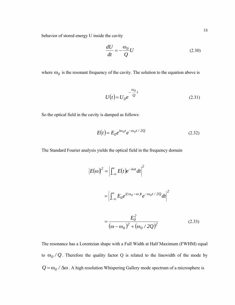
18behavior of stored energy U inside the cavity
UQdt
dU 0ω−= (2.30)
where is the resonant frequency of the cavity. The solution to the equation above is 0ω
( )t
Q0
0
eUtUω
−= (2.31)
So the optical field in the cavity is damped as follows:
( ) Q2/tti0
00 eeEtE ω−ω= (2.32)
The Standard Fourier analysis yields the optical field in the frequency domain
( ) ( )2
ti2 dtetEE ∫∞∞−
ω−=ω
2
Q2/tt)(i0 dteeE 00∫
∞∞−
ω−ω−ω=
( ) ( )20
20
20
Q2/E
ω+ω−ω= (2.33)
The resonance has a Lorentzian shape with a Full Width at Half Maximum (FWHM) equal
to . Therefore the quality factor Q is related to the linewidth of the mode by
. A high resolution Whispering Gallery mode spectrum of a microsphere is
Q/0ω
ω∆ω= /Q 0

19
Figure 2.4. High resolution whispering gallery mode spectrum. The quality factor is
2×10⁷ at 980 nm.
presented in figure 2.4, where the total quality factor is deduced from the linewidth of the
mode.
We recall the definition of the cavity quality factor given by (2.30), and the total quality
factor is decided by the total loss rate in the cavities. There are several loss mechanisms in
optical resonators, thus we can rewrite equation (2.30) as

20
U
WU
WU
WU
WU
WU
WQ
1 coupradscssmattot
tot ω+
ω+
ω+
ω+
ω=
ω=
3214444 34444 21factorQuality External
coup factorQuality Intrinsic
radscssmat Q1
Q1
Q1
Q1
Q1
++++= (2.34)
where accounts for materials absorption loss, denotes the scattering loss from
surface inhomogeneities, describe the loss caused by surface contamination,
represents the tunneling loss due to the curvature of the boundaries in the propagation path
of the mode, and describes the coupling loss to a coupler. The quality factor
describing the loss from materials absorption, scattering, surface contamination and
radiation are usually called “cold cavity quality factor” or “intrinsic quality factor”, while
, which accounts for the coupling to a external coupler, is designated as ‘external
quality factor’. As studied by Haus and his colleague, increase exponentially with
increasing size, and for air clad microspheres with radii larger than about 15 µm,
[18]. While the absorption of silica at the wavelength of 1.55 µm can be as
low as 0.2 dB/km, which corresponds to an absorption limited quality factor of 10
matQ ssQ
scQ radQ
coupQ
coupQ
radQ
11rad 10Q >
11.
Therefore absorption and surface scattering are the predominant loss mechanism for silica
microspheres with radii larger than 15 µm.
Materials Loss:

21The quality factor due to materials absorption can be determined by [10]:
λαπ
=n2Qmat (2.35)
where is the wavelength, is the refractive index of the materials at λ , and λ n α is the
linear attenuation in the resonator caused by materials absorption.
Scattering Loss:
The quality factor due to scattering loss by the surface homogeneity can be estimated by
[10]
B
RQ 220
2
ssσπ
λ= (2.36)
where and σ B are the rms size the correlation length of surface homogeneities,
respectively.
Radiation Loss:
The Quality factor associated with the radiation loss is shown to be [18]:
( ) ( )
( ) ( )
2
0sl0s1l2
s
0s1l0sl1
0
050
20s0
3s
2
rad
RknjRknjn
RknjRknjn
ZRnNcknlQ
−
−
+
⎥⎥⎥⎥⎥
⎦
⎤
⎢⎢⎢⎢⎢
⎣
⎡
⎟⎟⎠
⎞⎜⎜⎝
⎛γπ
−
⎟⎟⎠
⎞⎜⎜⎝
⎛γπ
ε= (2.37)

22
with ( )( )
( )lRkn
RknjRknjRkn
21l
200
001l
00l001 +−−=γ
−
( )( )
( )lRkn
RknjRknjRkn
21l
200
00l
001l002 +−+=γ +
where c is the speed of light in the vacuum, 0ε is the permittivity of free space,
is the free space impedance. 377Z0 ≈

23C h a p t e r 3
OPTICAL COUPLING BETWEEN FIBER TAPER AND WGM CAVITY
3.1 Introduction
In this chapter we will review various methods developed to excite microsphere modes.
The fiber taper is used as an efficient way to couple the light into and out of the
microcavities throughout this thesis work. The coupling between the fiber taper and
microsphere cavities is investigated in details.
3.2 General methods for coupling to microsphere and microcavities
The modes in the WGM type microcavities are highly confined and are not accessible by
free-space beam. Therefore employments of near-field couplers are highly required.
Numerous methods have been developed to excite the whispering gallery modes in
microsphere resonators. The evanescent coupling scheme in which an evanescent field
tunnels into the microsphere appears to be the most promising approaching without
disturbing the high Q property of the cavities. As depicted in figure 3.1, the prism can be
used to efficiently couple the light into and out of the microsphere [19], but it uses bulk
component and it is difficult to align it with microsphere. The polished half block coupler
provides is a robust way to couple the light into the microsphere but the coupling efficiency

24
(a) (b)
(c) (d)
Figure 3.1. Different coupling schemes for microspheres: (a) Prism coupler; (b)
Angle polished fiber tip; (c) Polished half block coupler; (d) fiber taper
is low because of the light coupled to the cladding radiation mode of the half block [20,
21]. The angle polished fiber is efficient to excite the microsphere modes, but it requires
delicate cutting of the angle and polishing the end of the fiber tip [22]. The fiber taper
coupler can not only to align with the microsphere but only efficiently couple the light into
and out of the microsphere cavities. In the following part, we will focus on the fiber taper
coupler.

253.3 Fabrication of the fiber taper
Figure 3.2. Optical image of waist of the fiber taper. Inset: a standard 125 µm single
mode optical fibers
The fiber taper is fabricated from a standard optical fiber. The fiber is first mounted on a
stage which can hold the fiber throughout all the experiment. Then the fiber is exposed to
the top zone of a hydrogen flame, where the temperature is high enough to melt the silica.
Right after the fiber become soft due to the heat absorption, two computer program
controlled motors begin to pull each end of the fiber to opposite direction. The pulling
process is stopped when the waist size of the fiber taper decreases to 1 to 2 µm. Figure 3.2
shows an optical image of a tapered fiber with waist diameter around 1 µm. The inset
presents an image of a standard SMF-28 optical fiber with diameter of 125 µm for
comparison.

263.4 Characterization of the fiber taper modes
Although the fiber taper is pulled from a fiber with core and cladding region, during the
pulling process the core vanishes and the fiber taper can be regarded as an air-clad cylinder
waveguides. The analytic solution for mode of propagation in cylinder waveguide is well
known. The characteristic equation which determines the propagation constant ( ) of the
fiber mode is [18]:
fβ
( )( )
( )( )f0
f1f
f0
f1f akK
akKakJakJ
k α= (3.1)
with 2f
2f
2f nkk β−=
2c
22ff nk−β=α
where a is the core radius of the fiber taper at the coupling zone, is the refractive index
of the fiber taper, and are Bessel function of the zero and first order, while and
are the modified Hankel functions of zero and first order.
fn
0J 1J 0K
1K
3.5 Coupling between the fiber taper and the cavity
Let’s consider excitation of a high Q WGM by a traveling mode in the fiber taper coupler.
Assume is the field amplitude of the whispering gallery mode, and in the ( )tEs iE oE

27
α
Es
Ei:Input Eo:Output
Figure 3.3. Schematic of cou
field amplitude of taper mode b
coupling of the resonator mo
coefficient of the field amplitud
into and out of the resonator ca
( ) (EitE is κ=
( ) ( )ttEtE io =
where L is the round trip dista
case, ), is the co0R2L π= κ
t
,ϕ
t′
κ′
pling
efore a
de wit
e befo
n be de
) tt '+
Ei 'κ+
nce tra
upling
κ
between fiber taper and cav
nd after the cavities, respectiv
h the fiber taper mode and
re and after the coupling regio
scribed by equations [23]:
( ) ( 2/LiexptE 0s α−ϕτ−
( )ts
veled by the mode inside the r
coefficient, which can be calc
ity
ely. Let describe the κ
t be the transmission
n. The coupling of light
) (3.2)
(3.3)
esonator (for the sphere
ulated as the normalized

28integral of the field of the cavity mode and the fiber taper coupler mode.
is the round trip time of the mode traveling inside the resonator,
c/Lns0 =τ
λπ=ϕ /Ln2 s is the
phase change of the mode after a round trip in the resonator, and α is the linear attenuation
in the resonator caused by absorption, scattering and radiation. Because of time reversal
symmetry and energy conservation, we have 'tt = , 'κ=κ , and 1t 22 =κ+ . For high
Q cavity, the round trip loss is very small, in other words 1<<α and 1<<κ . Assume
is the resonant frequency of the cavity mode. By expanding 00 /c2 λπ=ω ( )0s tE τ−
at t and ignore the high order term, i.e. ( ) ( ) ( ) dt/tdEtEtE s0s0s τ−=τ− , and replace
it in equation 3.2, we obtain
( ) ( ) ( ) ( )tE
titEi
dttdE
i0
s0cs
τκ
=ω∆+δ+δ+ (3.4)
where 0
c tt1
τ−
=δ , s
0 n2cα
=δ and ω∆ is the frequency shift to the resonant
frequency. According to definition of the quality factor, the equation for the field of the
mode in the resonator can also be written as
( ) ( ) ( )tEitEi
Q2Q2dttdE
is0
0
ex
0s γ=⎟⎟⎠
⎞⎜⎜⎝
⎛ω∆+
ω+
ω+ (3.5)
where is the intrinsic quality factor originating from the loss mechanism in the cavity
including scattering from surface, materials absorption due to molecule resonances, or
0Q

29whispering gallery radiation loss, is the external quality factor determined by the
coupling between the resonator and the coupler and
exQ
γ is the coupling coefficient of input
field coupled into the resonator [18]. Compare equation 3.4 with 3.5, the parameter 0δ and
can be related to the quality factor: cδ
0
00 Q2
ω=δ (3.6)
ex
0c Q2
ω=δ (3.7)
At steady state, the time derivative of ( )tEs is equal to zero, which means that
( ) ( ) ( )tEti
i1tE i
00cs ⎟⎟
⎠
⎞⎜⎜⎝
⎛τκ
ω∆+δ+δ= (3.8)
So the field amplitude can be changed by cδ for a given input power in the fiber taper
coupler and it reaches its maximum value at c0 δ=δ . The cavity buildup factor (B) is
( ) ex
2tot
s
020
2
2
2c0
2in
2s
Lnt1
E
EB
πλ
=τκ
δ+δ== (3.9)
The output field amplitude can be deduced from equation 3.3 and 3.8:

30
( ) ( ) ( ) ( )tEti
1tEtE i0
2
0cio ⎟⎟
⎠
⎞⎜⎜⎝
⎛
τκ
ω∆+δ+δ−=
( ) ( ) ( )tEi
2tE i0c
ci ω∆+δ+δ
δ−= (3.10)
And the normalized transmission of the cavitiy (T) is given by
( )( ) ( ) ( )22
c0
c02
i
2o 41
tE
tET
ω∆+δ+δ
δδ−==
( ) ( )20ex0
2ex0
ex0
/QQQQQQ41
ωω∆++−= (3.11)
Both the resonator buildup factor and transmission can be described as function of the
quality factors of the resonator, therefore the quality factors are very important parameter to
characterize the fiber taper coupled resonator. The intrinsic quality factor is a decided by
the resonator itself, while the external quality factor changes with the transmission
coefficient t, which changes with the geometry of the coupling (i.e. overlap between the
resonator mode and the fiber taper coupler mode). As noted in equation 3.11, the
transmission of the resonator is decided by the relation between the intrinsic quality factor
and controllable external quality factor . The intrinsic quality factor is a
constant for a given cavity, but the external quality factor changes with the loading
inQ exQ inQ
exQ

31
Figure 3.4. Different coupling regimes for a cavity with the intrinsic quality factor
Qo of 1×10⁸.
conditions. Figure 3.4 is a plot of the resonator transmission T against the phase shift for
different loading condition.
When the mode is on resonant in the cavities, the coupling between the waveguide and the
resonator can be divided into three regimes:

32(1) Under-coupled regime: Due to the loss mechanisms, the resonator has a limited
intrinsic quality factor . When the fiber taper is far away from the resonator, the
coupling between them is very weak and the overlap between the fiber taper mode
and resonator mode is close to zero, i.e.
inQ
1t → , and . When the fiber
taper get closer to the resonator, the overlap of the modes increase, decreases
but still larger than , then the transmission T decrease continuously from unity
and approaches zero gradually.
∞→exQ
exQ
inQ
(2) Critical-coupled regime: When the fiber taper get close to the resonator to a such
point (critical coupling point) that is equal to , the normalized
transmission is zero, which means that all the input power is coupled into the
cavity.
exQ inQ
(3) Over-coupled regime: When the fiber taper approaches the cavity further after the
critical coupling point, the overlap of the modes become larger and the
decrease further. The normalized transmission becomes smaller than 1 again and
it’s called over-coupled regime.
exQ
Figure 3.4 shows how the transmissions changed by the relation between the intrinsic
quality factor and the external quality factor. In addition, as can be seen from equation
3.11, the transmission of the mode is a function of the external quality factor, which
changes with the loading condition. Figure 3.5 shows the normalized transmission of the
mode as a function of the air gap between the fiber taper coupler and a microsphere with

33
Figure 3.5. Normalized transmission of a fiber taper coupled microsphere versus the
air gap between the microsphere and the taper.
diameter of 60 µm. In the under-coupled regime, the transmission decreases gradually
when the air gap decreases, and become zero at critical coupling, then it increases if the air
gap decrease further.
3.6 Phase matching between the microcavities and the fiber-taper coupler
The amount of power coupled out of the fiber into the sphere is proportional to
( )20exp β∆⋅γ− , where 0γ is constant decided by propagation constant and the fβ

34diameter of the microsphere and β∆ is the difference in the propagation constants
between the fiber mode and the sphere mode. The coupling efficiency is maximized at the
phase matching condition, where β∆ is equal to zero.
3.7 Conclusion
Fiber taper is proved to be very efficient in coupling light into and out of the resonator
throughout this thesis work. The transmission of the microcavity depends on the
configuration, i.e. the air gap between the fiber taper coupler and the microcavity and the
phase matching condition between the coupler and microcavity modes. To optimized the
coupling efficiency between the fiber taper and the microcavities, phase matching
condition need to be satisfied.

35C h a p t e r 4
OPTICAL MATERIALS BY SOL-GEL PROCESS
4.1 Introduction
The sol-gel method is a wet-chemical synthesis technique for preparation of oxide gels,
glasses, and ceramics at low temperature. It’s based on control of hydrolysis and
condensation of alkoxide precursors. As early as the mid-1800s, interest in the sol-gel
processing of inorganic ceramics and glass materials has begun with Ebelman and
Graham’s studies on silica gels [24]. The investigator recognized that the product of
hydrolysis of tetraethoxysilane (TEOS) under acidic conditions is SiO2. In the 1950s and
1960s Roy and co-workers used sol-gel method to synthesize a variety of novel ceramic
oxide compositions with very high levels of chemical homogeneity, involving Si, Al, Zr,
etc, which couldn’t be made using traditional ceramic powder methods [25-28]. It’s
possible to fabricate ceramic or glass materials in a variety of forms, such as ultra-fine
powers, fibers, thin films, porous aerogel materials or monolithic bulky glasses and
ceramics [29]. Since then powders, fibers, thin films and monolithic optical lens have
been made from the sol-gel glass.
4.2 An overview of sol-gel process steps

36The sol-gel process, as the name implies, involves transition from a liquid ‘sol’ (colloidal
solution) into a ‘gel’ phase [30]. Usually inorganic metal salts or metal organic compounds
such as metal alkoxide are used as precursors. A colloidal suspension, or a ‘sol’ is formed
after a series of hydrolysis and condensation reaction of the precursors. Then the sol
particles condense into a continuous liquid phase (gel). With further drying and heat
treatment, the ‘gel’ is converted into dense ceramic or glass materials. Generally three
reactions are used to describe the sol-gel process: hydrolysis, alcohol condensation and
water condensation. Because water and alkoxides are immiscible, alcohol is commonly
used as co-solvent. Due to the presence of the co-solvent, the sol-gel precursor, alkoxide,
mixes well with water to facilitate the hydrolysis.
(4.1) OHROHSiOHHORSi|
|
Hydrolysis|
|tionesterificaRe
−+−−⎯⎯⎯⎯ →⎯−+−−⎯⎯⎯⎯⎯⎯ ⎯←
During the hydrolysis reaction, the alkoxide groups (OR) are replaced with hydroxyl group
(OH) through the addition of water. Subsequent condensation reaction involving silanol
group (Si-OH) produces siloxane bonds (Si-O-Si) with by-product of water (water
condensation) or alcohol (alcohol condensation). As the number of siloxane group
increases, they bridged with each other and a silica network is formed. Upon drying, the
solvents that are trapped in the network are driven off. With further heat treatment at high
temperature, the organic residue in the structure is taken out, the interconnected pores
collapse and a densified glass or ceramics is formed.

37
4.2.1 Hydrolysis and condensation
Although hydrolysis can occur without additional catalyst, it has been observed that with
the help of acid or base catalyst the speed and extent of the hydrolysis reaction can be
enhanced. Under acid conditions, the alkoxide group is protonated rapidly. As a result,
electron density is withdrawn from the silicon atom, making it more electrophilic with
partial positive charges. Therefore it’s more susceptible to be attacked by the nucleophile,
water molecule. Subsequently a penta-coordinated transition state is formed with SN2 type
characters, where there is simultaneous attack of the nucleophile and displacement of the
leaving group. When the nucleophile attacks the center atom, Si, it’s on the opposite side to
the position of the leaving group, R-OH. Finally the transition state decays by breaking of
the Si-OHR bond and ends up with an inversion of silicon configuration as shown in
equation 4.2. The acid-catalyzed mechanism can be described as following:
ROSiHORSi|
H
|
|
Fast|
|−−−⎯⎯ →⎯+−−
+
⎯⎯←
+ (4.2)
OHROHSiOSiOHOHROSi|
|
H
H|
R
HH
|
| |−+−−⎯→⎯⎥
⎦
⎤⎢⎣
⎡−−⎯→⎯−+−−−
⎯⎯←
+∨
⎯⎯←
••+
Under basic conditions, the hydroxyl anion works as nucleophile and attacks the silicon
atom. Again, an SN-2 type mechanism has been proposed in which OH displaces OR

38group with inversion configuration of the silicon tetrahedron. The mechanism of the
base-catalyzed mechanism can be described as following:
HOSiORHOSiORHOORSi||
|
|−−−−⎯→⎯⎥
⎦
⎤⎢⎣
⎡−−−−⎯→⎯+−−
∨−
⎯⎯←
−∨
⎯⎯←
−••
(4.3) −
⎯⎯←+−−⎯→⎯ ROOHSi
|
|
4.2.2 Gelation
In the gelation step, alkoxide gel precursor undergoes polymerization (condensation)
reaction with by-product of water or alcohol. Similar to hydrolysis, the condensation
reaction is also affected the acid/base catalyst. With the existence of acid catalyst, weakly-
crosslinked polymer is formed and can easily aggregate after drying yielding low-porosity
microporous structure. On the contrary, if base catalyst is used, discrete highly branched
clusters are formed and lead to a mesoporous structure after gelation.
(4.4) OHHSiOSiOHSiOHSi|
|
|
|
onCondensatiWater|
|
|
|Hydolysis
−+−−−−⎯⎯⎯⎯ →⎯−−+−−⎯⎯⎯⎯ ⎯←
(4.5) OHRSiOSiRSiOHSi|
|
|
|
onCondensatiAlcohol|
|
|
|sAlcoholysi
−+−−−−⎯⎯⎯⎯ →⎯−−+−−⎯⎯⎯⎯ ⎯←

39
4.2.3 Ageing
The continuing chemical and physical changes during ageing after gelation are very
important. During this process, further cross-links continuous, the gel shrinks as the
covalent links replace non-bonded contacts and the pore sizes and pore wall strengths
change with the evolution of the gel’s structure.
4.2.4 Drying
The gel has a high ratio of water and three dimensional inter-connected pores inside the
structure. Before the pore is closed during the densification process, drying is needed to
remove the liquid trapped in the interconnected pores. On the other hand removal of the
liquid from the tiny pores causes significant stress resulting from inhomogeneous
shrinkage. Therefore the main problem that had to be overcome is cracking due to the large
stress in the structure. For small cross sections, such as powder, coating, or fiber, the drying
stress is small and can be accommodated by the materials, so no special care is needed to
avoid cracking for those sol-gel structures. While for monolithic objects greater than 1 cm,
drying stress developed in ambient atmosphere can introduce catastrophic cracking, as a
result control of the chemistry of each processing step is essential to prevent cracking
during drying.
4.2.5 Densification
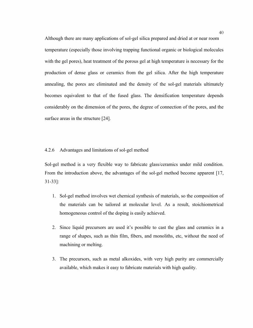
40Although there are many applications of sol-gel silica prepared and dried at or near room
temperature (especially those involving trapping functional organic or biological molecules
with the gel pores), heat treatment of the porous gel at high temperature is necessary for the
production of dense glass or ceramics from the gel silica. After the high temperature
annealing, the pores are eliminated and the density of the sol-gel materials ultimately
becomes equivalent to that of the fused glass. The densification temperature depends
considerably on the dimension of the pores, the degree of connection of the pores, and the
surface areas in the structure [24].
4.2.6 Advantages and limitations of sol-gel method
Sol-gel method is a very flexible way to fabricate glass/ceramics under mild condition.
From the introduction above, the advantages of the sol-gel method become apparent [17,
31-33]:
1. Sol-gel method involves wet chemical synthesis of materials, so the composition of
the materials can be tailored at molecular level. As a result, stoichiometrical
homogeneous control of the doping is easily achieved.
2. Since liquid precursors are used it’s possible to cast the glass and ceramics in a
range of shapes, such as thin film, fibers, and monoliths, etc, without the need of
machining or melting.
3. The precursors, such as metal alkoxides, with very high purity are commercially
available, which makes it easy to fabricate materials with high quality.

414. It’s cost effective because the temperatures required in the process are low, close
to room temperature, and no delicate vacuum system is needed.
Despite all the advantages, sol-gel method still has some limitation. Solvents, such as
alcohol and water, are involved in the process, so it’s not appropriate for fabrication which
is very sensitive to solvents. Furthermore, stress induced cracks upon drying are not unusal
and can’t be healed after densification. Very careful attentions are needed to avoid
cracking. Despite of the disadvantages, sol-gel method is a very mild and flexible method
to fabrication materials that possess properties not attainable by other methods. It inspires
us to further investigate and modify the method to exploit its maximum value in
application.
4.3 Fabrication of sol-gel films for photonic application
(a) (b) (c)
Figure 4.1. Schematic of fabrication of sol-gel films on a substrate: (a)
organometallics and dopants in alcohol solvents (b) hydrolysis of organometallics in
water (c) sol-gel films on a substrate by dip-coating or spin-on methods.

42Figure 4.1 shows a schematic of the preparation procedure of sol-gel films on a glass or
silicon substrate. First, organometallics (such as metal alkoxides) and dopants are put in an
alcohol solvent, such as ethanol or isopropanol. Then the water is added to hydrolyze the
organometallics. After hydrolysis and condensation reaction for certain time (ranges from
several hours to several days under different condition), a viscous gel is formed. After
aging the sol solution at room temperature, a layer of sol-gel film is deposited on a
substrate by spin-on or dip-coating method. The thickness of the films is decided by the
viscosity of the sol solution, the spin speed for the spin-on method, or dipping time for the
dip-coating method.
4.4 Characterization of sol-gel silica film with Fourier Transform Infrared Spectrometer
(FTIR)
Infrared spectroscopy is the study of the interaction of infrared light with matter [34].
When infrared radiation interacts with matter it can be absorbed, causing the chemical
bonds in the materials to vibrate. Chemical structures within molecules, known as
functional groups, tend to absorb infrared radiation in the same wavenumber range
regardless of the structure of the rest of the molecules. The correlation between the
wavenumber and molecule structures makes it possible to identify the structure of unknown
molecules. For instance, the peaks around 3000 cm-1 are due to C-H stretching bond.
A series of thin films were annealed at different temperatures, ranging from 200° C to
1200° C. A Fourier Transform Infrared (FTIR) microspectroscope was used to compare the

43structure of sol-gel silica with that of thermally grown silica. Figure 4.2 shows the
evolution of the reflectance infrared spectra as a function of annealing temperature. The
characteristic
1200 1000 800 600 400
1200 0C
1000 0C
800 0C600 0C400 0C
Ref
lect
ion(
a.u.
)
Wavenumber (cm-1)
200 0C
thermal Silica
Figure 4.2. FTIR spectra of thermal silica and sol-gel silica samples prepared with
different heat treatment.
vibrational bands of silica were found in the spectra of sol-gel silica. Compared with FTIR
spectrum of thermally grown silica film, the absorption band, which correspond to Si-O-Si
bending (near 460 cm-1), Si-O-Si symmetric stretching (near 810 cm-1), and Si-O-Si

44asymmetric stretching (near 1105 cm-1) are clearly shown in figure 4.2 [35]. When the
annealing temperature is 200° C, a weak absorption band at ~964 cm-1 is observed, which
is attributed to stretching vibration of silanol Si-OH hydrogen bonded groups. The
excited Er3+ can be quenched through non-radiative relaxation by coupling to a
quenching site, such as hydroxyl group OH-. This absorption band disappears at
temperature of 600 °C. In addition, compare with the spectra of others, the spectra of the
sample heated at 1000° C and 1200° C have stronger, broader and blue-shifted Si-O-Si
bands. The changes in the spectra indicate the complete densification of silica films after
heat treatment [36]. Furthermore, as the temperature is increased, the absorption band due
to Si-O-Si bending becomes stronger. It shows that the crosslink between silica chains are
improved gradually due to progressively enhancement of condensation reaction under
higher densification temperature. The spectra of the samples heated at 1000° C and 1200°
C are similar to that of the thermally grown silica.
4.5 Effect of anneal temperature on etching rate of sol-gel film in buffered Fluoride acid
(HF)
To further probe the change of the microstructure of the glass, hydrofluoric acid (HF)
etching was used to monitor the subtle change of the glass after different heat treatment.
The silicate structure with smaller Si-O-Si bond angles are more vulnerable to HF than
structure with larger bond angles [37]. During the etching rate test experiments, the
etching rate of films annealed at temperature lower than 600° C has etching rate of more
than 1000 Å/s. When samples are annealed at 1000° C and 1200° C, the etching rate

45decreases to 15 Å/s, which is almost the same as that of the thermally grown silica (13
Å /s). This result is consistent with the blue shift of the Si-O-Si bond in FTIR which
indicates an increase of the average Si-O-Si bond angles [38]. The etching rate
experiment confirms that the microstructure of the sol-gel silica annealed at temperature
as high as 1000 °C is the very close to that of the thermally grown silica.
4.6 Conclusion
In this work, silica thin film has been prepared by the sol-gel method. A Fourier Transform
Infrared Spectroscopy (FTIR) is used to analyze the composition of the silica sol-gel
prepared in the lab. It shows that the sol-gel silica annealed at temperature at or above 1000
°C is very similar to thermal silica. Furthermore the etch rate in buffered HF solution of
thin films annealed at different temperature was investigated. The etch rate of the films has
been shown to change by almost two orders of magnitude for undensified and densified
sol-gel films. This result can later be used to selectively coat the surface of a microtoroid
cavity on a silicon chip which will be discussed in chapter 6.
.

46C h a p t e r 5
SURFACE FUNCTIONALIZATION OF SILICA MICROSPHERE RESONATORS
5.1 Introduction
Microcavities formed by surface tension (droplets and solid spheres or spheroids) can
exhibit quality factors in excess of one billion and are of interest in cavity QED, nonlinear
optics, photonics and sensing. When silica microspheres are doped using any number of
rare earth ions, ultra-low threshold micro lasers are possible [3, 12, 39]. The preparation of
these devices requires acquisition of bulk samples of rare-earth doped glass that are
subsequently processed into a spherical cavity. Here, an alternative to this process is
presented in which ready-made microspheres of undoped silica serve as a base resonator
structure and gain functionalization of the surface is performed using an erbium-doped sol-
gel film. Sol-gel films are readily doped with a number of different rare earth ions [40-42],
as well as other materials [43, 44], thereby making this a more versatile method for
preparation of active microspheres. In addition, the sol-gel preparation process allows for
precise control of dopant concentration, making possible the study of a range of inversion
concentrations. Finally, it will be shown that the thin film nature of the gain layer has an
important effect on laser dynamics.
5.2 Erbium doped silica glass

47
Figure 5.1. Schematic representation of the Er3+ intra 4f Energy level.
Rare earth atoms are divided into two groups: the lanthanides with atomic number from 57
to 71, and the actinides with atomic number from 89 to 103. The vast majority of rare earth
doped amplifiers and lasers use lanthanides elements as gain medium. Among them erbium
(with atomic number 68) doped amplifiers and lasers are especially interesting due to the
erbium 4f transition which falls in the 1.5 µm telecommunication window.
Erbium usually takes the ionic form, in particular the trivalent state, Er
2/154
2/134 II →
3+. The atomic

48configuration of the Er3+ is (Xe)4f11, where (Xe) represents a Xenon core. The shielding
of 4f electron from the environments by the outmost 5s and 5p electrons is responsible for
erbium’s rich optical spectrum. Due to various atomic interactions between electrons, the 4f
electron spread in different energy level. A further splitting of the energy level arise when
erbium are doped in a glass host materials. The local electric field in the glass matrix
breaks the spherical symmetry of the rare earth ions. Thus the degeneracy of the 4f atomic
states will be lifted to some degree and the splitting is referred to as Stark splitting of the
energy level. As can be seen from the energy level diagram in fig. 5.1, the Erbium ion can
be excited by pump wavelength of 1.48 or 0.98 µm.
5.2.1 Er3+-Er3+ interactions
The intra-4f transitions are ‘forbidden electronic dipole’ in nature, so the Er3+ has very
small absorption/emission cross section, on the order of 10-21 cm2. It has been found that
when the Er3+ concentration is high in order to obtain adequate gain, undesirable effect
occurs. These effects can be related to certain Er3+-Er3+ interactions. When the local
concentration of Er3+ becomes high enough, it’s not valid to assume that each ion is
isolated and independent of its neighbors. On the contrary, when two ions get close enough,
energy can migrate from one ion to another, which has a negative impact on the energy-
donor ions. There are several erbium ion interactions, among which two mechanisms
prevail.
Cooperative Upconversion

49When ions 1 and 2 are both in the upper laser level , The radiative lifetime around
10 ms in a silica glass gives closely spaced neighbors enough time to interact. During the
upconversion process, ion 1 transfers energy to ion 2 and drops back non-radiatively to the
ground state. At the same time, ion 2 is promoted to higher energy level, usually ,
from where it rapidly relax non-radiatively back to the excited state or relax
radiatively to the ground state with emission of one photon at 540 nm, which corresponds
to the green light observed throughout this work. In this case, the ions are independent
which means that if one ion in the excited state does not prevent the neighboring ion
from being excited to the state . Up-conversion depends on whether both ions are
exited to the state.
2/134I
2/94 I
2/134I
2/134I
2/134I
2/134I
Pair induced quenching
Similar to the cooperative up-conversion it involves energy transfer between two excited
ions. The ions are so closely coupled that one ion will transfer its energy to the other one in
a time scale that is significantly faster than the pump rate. But in this case the ions are no
longer considered to be independent, and the ions should be treated as paired ions, instead
of single ions. This effect will be discussed in details in chapter 8.
5.3 Fabrication of silica microsphere

50
(a)
(b)
(c)
(d)
Figure 5.2. Illustration of fabrication of the microsphere for a silica fiber. (a) single
mode silica fiber (b) A fiber taper is formed (c) Use very strong CO2 laser to
irradiate at A, at the same time pull the fiber quickly to break the fiber taper at spot
A. (d) Irradiate the fiber tip with CO2 laser, and due to surface tension a
microsphere is formed with the left fiber as a supporting stem.

51
Figure 5.3. Transmission spectrum of a fiber taper coupled microsphere with
diameter of 39 µm.
Silica has a very low loss in the 1550 nm band and is therefore an excellent material for
preparation of ultra-high-Q microspheres. In addition, because silica has a strong
absorption for CO2 laser at 10.6 µm, a SYNRAD 10W CO2 laser is used a as a heat source
during the microsphere fabrication process. A CCD camera connected with a display
screen is used to monitor the microsphere fabrication process. Figure 5.2 shows an
illustration of the fabrication of the ultra-high-Q microspheres. First the plastic cladding of
a standard silica optical fiber is removed and the core region with a diameter of 125 µm is

52exposed to the air. Some volatile solvent, such as ethanol or isopropanol, is used to clean
the surface of the core. Then the CO2 is used to heat certain region of the fiber,
simultaneously the fiber is pulled gradually until the waist diameter is about 5~20 µm.
Then the heating point moves to fiber region A which is a little shifted from the waist area
as show in fig. 5.2c. A very strong CO2 laser is used to irradiation at A while the fiber is
pulled quickly, as a result the fiber can not sustain the quick pulling and breaks at the soft
point A. Afterwards, the fiber tip is heated and a microsphere is formed due to surface
tension. The left fiber works as a supporting stem for the microsphere. Figure 5.3 shows a
transmission spectrum of a fiber taper coupled microsphere.
5.4 Surface functionalization of microsphere
Figure 5.4 shows a schematic for surface functionalization of a silica microsphere. First the
sol gel starting solution was prepared by hydrolyzing tetraethoxysilane (TEOS) in water
under acid conditions (pH~1) with isopropanol as the co-solvent. Er ions were introduced
by adding ErNO3⋅5H2O with a weight ratio of ErNO3⋅5H2O/TEOS∼0.2wt% [45]. The
mixture was then stirred vigorously at 70°C for ten hours. After aging the sol solution at
room temperature for another ten hours we immersed silica microspheres in the solution.
The initial pure-silica microspheres were formed by heating the end of a tapered fiber tip
with a CO2 laser as described by Knight [46]. Multiple process cycles were used to build up
a desired layer thickness. Each process cycle consisted of dipping the sphere for 20 minutes

53
Figure 5.4. Schematic of surface functionalization of silica microsphere.
in the sol gel solution followed by heating in an oven at 160°C for 10 minutes. The layer
thickness obtained in a processing cycle depended on the dipping time and solution
viscosity. In this experiment, the build-up rate was estimated to be about 0.3 µm/cycle
(determined by observation of layer thickness after multiple cycles). Every two cycles, the
spheres were irradiated using the CO2 laser for several seconds. The laser intensity was
sufficient to induce flow and densification of the sol gel layer. In addition, micro-cracking
that was present in the sol gel surface was annealed out by this process. By repeating this
process, the coating thickness was varied. Silica spheres ranged in diameter from 50 to 80

54µm and the coating thickness was varied from 1 to tens of microns. The Er3+ doping
concentration of the resulting doped shell was estimated to be around 1019 cm-3.
5.5 Coupling between fiber taper and microsphere
Optical coupling to the spherical microcavities both for the purposes of pumping as well as
laser output extraction was performed using optical-fiber tapers. Taper coupling has been
used previously to demonstrate microsphere-lasers in the telecommunication band. It
makes possible the resonant excitation of specific whispering gallery modes and efficient
pumping of a small gain volume within the sphere. As shown in fig. 5.5, the pump power
was transmitted and coupled into the microsphere from one end of the fiber taper and the
laser output was extracted and transmitted to some optical receivers connected to the other
end. The typical waist diameter of the tapers used to couple pump power and collect laser
emission was around 1.6 µm.
Whispering gallery mode (WGM) resonances correspond to light trapped in circulating
orbits just within the surface of the spheroidal particle [47, 48]. The modal indices are
similar to those used to characterize simple atomic systems with radial (n), orbital (l),
azimuthal (m) and polarization (TE or TM) indices needed to completely specify a mode.

55
Figure 5.5. Schematic of a thin film coated microsphere laser coupled with a fiber
taper. Red and green arrows represent input pump and output lasing waves,
respectively.
In particular, the angular distribution of the modes is given by the spherical harmonics
Ylm(θ,ϕ) (see figure 5.6) and the WGM modes with best spatial overlap to the fiber taper
have their power concentrated near the equatorial plane (m≈l) with a low radial coordinate
n≈1. These same modes are also best able to pump the active medium surface layer over a
radial thickness given approximately by the material wavelength of the pump band. The
pumped region will overlap with the emission band modes enabling lasing action. For a
surface layer thickness somewhat less than the radial width of the pump mode, nearly
complete inversion is expected within annular shaped equatorial bands. Conversely, when
the thickness is substantially greater than the pump-mode radial width there will remain

56unpumped regions that can provide saturable absorption to the longer-wavelength lasing
modes. In addition to modifying the threshold characteristics, saturable absorption is
known to modify lasing dynamics such that pulsation behavior is possible. This distinction
between thick and thin shell behavior is investigated below.
(b)(a)
Figure 5.6. Image of the WGMs in the taper-sphere coupling zone: (a) l-m=1. (b) l-
m=4. The green rings are up-converted photoluminescence. The inset shows
spherical harmonics Ylm(θ,ϕ) for (a) l-m=1 and (b) l-m=4
5.6 Laser performance
The pump wave was in the 980nm wavelength band, and provided by a tunable single
frequency, narrow-linewidth (<300kHz), external-cavity laser. The pump wavelength was
scanned initially to survey pumping modes. These were observable by monitoring the
transmission versus tuning and also by using a camera to monitor green, excited-state
emission from the sphere as the pump laser tuned into resonance with various pump modes.

57Figure 5.6 shows representative lateral emission distributions observed for different
WGMs in the sphere-taper coupling zones. The pump power coupled to the sphere was
measured as the difference of the launch power into the taper and the transmitted power
after the taper.
1500 1510 1520 1530 1540 1550 1560 1570-70
-60
-50
-40
-30
-20
-10
Lase
r Out
put (
dBm
)
Wavelength (nm)
Figure 5.7. Emission spectrum of a microsphere laser
A typical laser spectrum for cw operation is presented in figure 5.7. This was measured
using an optical spectrum analyzer with resolution bandwidth setting of 0.5nm. Multi-line
operation was also observed and depended upon the pump wavelength selected. However,

58by tuning the pump wave it was always possible to achieve single line operation. This is
believed to result from strong spatial mode selection possible when the so-called
whispering gallery mode (equatorial ring orbit) is resonantly pumped. Figure 5.8 shows the
laser output versus the pump power absorbed by the microsphere for cw operation. The
0 100 200 300 4000
1
2
3
4
5
6
Lase
r Out
put(µ
W)
Absorbed Pump Power(µW)
Figure 5.8. Laser output power versus absorbed pump power in the microsphere
laser.
threshold was estimated to be around 28µW and the laser reaches an output power of 6µW.
Above threshold, the laser output power varied linearly with absorbed pump power. A laser
output power of up to 10µW was observed for single-mode pm operation. For convenience

59during the experiments, the sphere was in contact with the taper (i.e., zero air gap). This
greatly restricted control of coupling and potentially limited the optimization of laser output
power. In addition, optimal coupling of the pump requires balancing of taper loading with
round-trip loss (dominated by erbium absorption in the shell layer). Optimal coupling of
laser emission also requires optimization of loading, but not necessarily for the same
conditions as for the pump. Other factors affecting coupling are phase matching and field
overlap between the taper and sphere modes in both the pump band and the emission band.
5.7 Effect of doping thickness on the laser dynamics
Erbium-doped fiber lasers have shown pulsing operation. If a saturable absorber effect is
incorporated in the rate equations, a self-pulsing operation can be expected under certain
circumstance. There are two possible saturable absorber mechanisms for the Er3+-doped
microcavities. First, there may be a small amount of rare earth which has absorption line
close to the Er3+ laser but remain unpumped. The second possibility is a group of clusters
where the space between the neighboring Er3+ is so close that they can exchange energy
nonradiatively, subsequently some Er3+ originally pumped remain effectively unpumped
and serve as saturable absorbers. Both effects drain the upper laser level and may lead to
instability of the laser output.
Both continuous wave (cw) operation and pulsation mode (pm) operation were possible by
controlling the sol gel coating thickness. CW laser operation was observed with coating
thickness in the range of 1 micron, while pm laser operation was possible for coatings

60around or above 5 microns in thickness. The thickness of the doped layer was estimated
by observing the thickness of the sphere both before and after the coating process.
0.0 0.3 0.6 0.9 1.2 1.50
50
100
150
200
250
Rel
axat
ion
Osc
illat
ion
Freq
uenc
y(kH
z)
Sqrt(P/µW)
Figure 5.9. Measured pulsation frequency versus the square root of the laser output
power P
Figure 5.9 shows the measured pulsation frequency versus the square root of the laser
output power for pm operation. The frequency was in a range from tens of kilohertz to
several hundred kilohertz. An electrical spectrum analyzer was employed for this

61measurement. The observed linear behavior is consistent with un-damped relaxation
oscillations [49]. The ability to induce pm operation by control of shell thickness is
attributed to unpumped inner regions of the shell that can provide saturable absorption to
the lasing mode. This conjecture is consistent with the observation of pm operation in prior
microsphere laser work using bulk-doped glass for sphere fabrication. Azimuthal surface
regions can also potentially provide saturable absorption. However, if present here, they
were alone insufficient to induce instability.
5.8 Conclusion
In conclusion, we have demonstrated the gain functionalization of silica microspheres
using doped sol gel films. This technique provides a way to achieve a range of possible
gain media in the microsphere system. Likewise, other possible surface layers that target
applications such as nonlinear optics in a micro-cavity may also benefit from this approach
[11]. An important feature of the sol gel gain layer is the ability to quench previously
observed pulsations in these devices, thereby achieving continuous wave laser operation.
For shell thickness in the range of 1 micron, continuous wave laser operation was observed.
This behavior as well as the onset of pulsations for thicker active shells is attributed to
unpumped and hence saturable absorbing regions that can be present in thick shells.
62C h a p t e r 6
SURFACE FUNCTIONALIZATION OF SILICA MICROTOROID RESONATORS ON A SI CHIP
6.1 Introduction
Whispering-gallery type microlasers in which the cavity boundary is defined by surface
tension (e.g., spheres and droplets) have attracted much attention because the combination
of their very small mode volume and high, cold-cavity Q-factor enables ultra-low-threshold
operation [3, 12, 50]. Recently, a new class of ultra-high-Q, surface-tension-induced
microcavities fabricated on a silicon chip have been demonstrated. These structures feature
a toroidal-shaped cavity and enable the integration of electronics and other functions with
ultra-high-Q devices. In this paper we demonstrate surface-functionalization of these
devices using erbium-doped sol-gel films. To the authors’ knowledge, this is the first
demonstration of a wafer-based rare-earth doped microlaser. In addition to being integrable
with other optical or electric components, they are directly coupled to optical fiber using
fiber tapers.
We have previously applied the surface functionalization method using silica microsphere
resonators. Erbium-doped microlasers are especially interesting because their emission
band falls in the important 1.5 µm window used for optical communications. However,
microspheres, while useful as laboratory demonstration vehicles, are not suitable for
integration with other optical or electronic functions. Their properties are also difficult to

63
Figure 6.1. Optical micrograph top view of a microtoroid showing principal and
minor diameters of the toroid.
control during fabrication. In contrast, microlasers on a chip can be fabricated in parallel
and have characteristics that are more easily controllable using wafer-scale processing
methods.
6.2 Characterization of Microtoroid cavities
Like all whispering-gallery type microresonators, microtoroids feature optical modes that
are confined near the resonator periphery. The thickness of the microtoroid is generally
much smaller than the microtoroid diameter. Thus, in contrast to microspheres, these
structures support fewer azimuthal modes. This facilitates single-mode operation in the
microtoroids. Figure 6.2 shows field intensity distribution of the modes for toroids with the

64
(a) (b)
(c)
Figure 6.2. Simulation of fundamental TM modes for toroids with minor diameters
of (1) 4 µm (b) 8 µm and (c) 16 µm. Their principal diameters are all 70 µm.

65
1.2 1.3 1.4 1.5 1.6 1.7 1.8 1.90.0
0.2
0.4
0.6
0.8
1.0
D=70µm,d=16µmD=70µm,d=8µm
D=70µm,d=4µm
Nor
mal
ized
Fie
ld In
tens
ity
Polar Angle
sphere D=70µm
Figure 6.3. Field intensity distributions along the polar direction for different
microtoroids.
same principal diameter, but different minor diameters. To further demonstrate the
compression effect, in fig. 6.3 we plot the normalized field intensity along the polar
direction at a radial location with maximum intensity. The compression of the modes in the
polar direction is stronger with decreasing minor diameters. As the minor diameter increase
gradually, the mode profile approaches that of the microsphere.

66
Figure 6.4. Schematic of surface functionalization of a microtoroid on a silicon chip
6.3 Surface functionalization of microtoroid cavities on a Si chip
Figure 6.4 shows a schematic for surface functionalization of a silica microtoroid cavity on
a Si wafer. Silica toroid-shaped microresonators supported by a circular silicon pillar were
fabricated upon a silicon wafer containing a 2 µm layer of thermal silica (SiO2) [51]. The
sol-gel starting solution was prepared as described in chapter 5. After aging the sol-gel
solution at room temperature for 10 hours, we immersed silica microtoroids in the solution
for 3-5 hours. Then the wafers were heated in an oven at 160°C for another 10 hours to
drive off surface water. Microtoroids were then irradiated with a CO2 laser (10.6 µm
emission) in order to reflow and densify the sol-gel films. The CO2-laser emission is

67selectively absorbed by the silica layers. This and the relatively high thermal
conductivity of silicon (~100 times more thermally conductive than silica [52, 53],) leads to
selective reflow and densification of sol-gel at the all-important toroid periphery. Sol-gel
deposited elsewhere was unaffected by this process step. Because of the large difference
between the etching rate of densified and undensified silica films in buffered HF, sol-gel
deposited on all regions of the wafer other than the densified perimeter of the toroid could
subsequently be selectively removed. Microtoroids ranging in diameter from 60 to 85 µm
were fabricated and the Er3+ concentration in the sol-gel layer was estimated to be around
1019 cm-3.
6.4 Fiber taper coupled microtoroid lasers on a Si chip
An important feature of gain functionalization of the surface is that it puts optical gain only
where it is needed, i.e., where best overlap is possible with the fundamental whispering-
gallery modes. Figure 6.5 illustrates both a sol-gel functionalized microtoroid and the taper
coupling configuration used to both provide optical pumping and to extract laser optical
power. Figure 6.6 is a photomicrograph showing a taper-coupled microtoroid laser. The
pump wave was provided by a tunable, single-frequency, external-cavity laser operating in
the 980 nm band and having a short-term linewidth less than 300 kHz. The sample chip
was held in a rotator that was mounted upon a 3-axis translator for position control. Two
CCD cameras were used to monitor the microtoroid samples and the taper, providing both

68
Figure 6.5. Illustration showing a micro-chip laser consisting of an Erbium-doped
sol-gel thin film applied to a microtoroid. Also shown is a fiber taper used for both
pump coupling and laser emission extraction.
Figure 6.6. Photomicrograph top view of an Erbium microtoroid laser coupled by a
fiber taper.

69
1510 1520 1530 1540 1550 1560-65-60-55-50-45-40-35-30-25
Lase
r Out
put (
dBm
)
Wavelength (nm)
Figure 6.7. Emission spectrum of a microtoroid laser with approximate diameter of
80 µm.
horizontal and vertical views. The angle of the microtoroid relative to the taper was
adjusted using the rotator to align the taper with the equatorial plane of the toroid.
An optical spectrum analyzer (OSA) with resolution of 0.5 nm was used to measure the
laser emission. A typical laser spectrum is presented in fig. 6.7. Single line emission
(within the resolution of the OSA) was most often observed, however, at increased
pumping levels it was sometimes possible to induce oscillation in other longitudinal modes.

70
0 10 20 30 40 500.00.10.20.30.40.50.00.40.81.21.62.0
Reference Laser(b)
Frequency Detuning (MHz)
Lase
r Am
plitu
de (a
.u.)
(a) Microtoroid Laser
Figure 6.8. (a) Laser emission spectrum from Er-doped sol-gel thin-film coated
microtoroid laser. (b) Reference laser emission spectrum from a 1550 nm single-
mode laser with short-term linewidth of 300 kHz. Both spectra were measured using
a high finesse scanning Fabry-Perot spectrometer.
To further resolve the single line observed in the OSA scan of fig. 6.7, a high finesse
(~5000) Fabry-Perot etalon having a resolution of a few megahertz was also used to
analyze the laser spectrum. A single-frequency, tunable, external-cavity laser emitting in
the 1500 nm band and with known short-term linewidth of 300 kHz was measured as a
reference. Both spectra are presented in fig 6.8.

71
0 10 20 30 40 50 60 700.0
0.5
1.0
1.5
2.0
2.5
3.0
Lase
r Out
put (µW
)
Absorbed Pump Power (µW)
Figure 6.9. Measured laser output power plotted versus absorbed pump power for
a microtoroid laser with a diameter of 80 µm.
The measured laser output power plotted versus the absorbed pump power is shown in
figure 6.9. The threshold pump power in this data is 34 µW by extrapolation of the linear
lasing region. The differential quantum efficiency was measured to be as high as 11% for
the single-mode, unidirectional operation. During measurements, the microtoroids were in
contact with the taper. While this creates a very stable coupling, it prevents optimization of
the pump and emission coupling efficiencies. As a result, it might be possible to further

72reduce the threshold in more optimally coupled structures. The effect of optimization of
coupling will be part of a future study employing an improved experimental setup.
6.5 Conclusions
In summary, we have demonstrated Erbium-doped microtoroid lasers on a chip by use of
a sol-gel surface-functionalization technique. Single-line laser emission and threshold
pump powers as low as 34 µW were observed. Future work will be directed towards
studies of optimal coupling and potential integration with other devices.

73C h a p t e r 7
FABRICATION AND CHARACTERIZATION OF MICROTOROID LASERS ON A SI CHIP
7.1 Introduction
Optical gain can be generated by a nonlinear optical process, Stimulated Raman Scattering
(SRS), or rare-earth ions as a gain medium. These effects are the basis for a variety of
devices, such as Raman amplifiers/lasers and rare-earth ions-doped amplifiers/lasers [11,
54-56]. In Raman laser, the gain appears at frequency shifted from the pump wave by an
amount corresponding to the frequency of materials molecular vibration. While in rare-
earth doped lasers, the operating wavelength are determined by the energy level of dopants,
instead of the host materials itself. Many different rare-earth ions, such as erbium,
neodymium, thulium, etc, can be used to realize amplifiers operating at different
wavelength covering from visible to infrared light.
Recently, a chip-based silica resonator structure in the form of a microtoroid has
demonstrated ultra-high-Q-factors in the range of 100 million [51]. By coating these high-
Q microcavities with erbium-doped solgel films or by beginning with erbium implanted
silica layers, low threshold rare-earth-doped microlasers on a chip have been demonstrated
[57, 58]. In another study, the realization of integrated Raman microlasers beginning with a
layer of thermally-grown silica has been achieved [59]. The fabrication of both low
threshold Raman microlasers and Rare-earth doped microlasers made from silica-on-silicon

74is especially interesting because they are integrable with other optical or electronic
components and make integrated photonics circuits possible [57-59]. A number of methods
have been used to fabricate SiO2 films on silicon substrate, such as flame hydrolysis
deposition and chemical vapor deposition [60, 61]. An alternative route to fabricate silica
films is the sol-gel technique. Compared with other methods, the sol-gel method has
several advantages: First, it is a versatile technique that involves wet chemical synthesis,
therefore the chemical composition of the materials can be stoichiometrically controlled at
the molecular level, and the distributions of dopants are homogeneous. Second, it is cost
effective due to reaction at low temperature without expensive and delicate vacuum system.
This technique allows a wide variety of thin films to be deposited on various substrates.
Different optical devices, such as erbium doped waveguide amplifiers (EDWA), one-
dimensional photonics crystal devices, microlenses, external-cavity distributed Bragg
reflector and size-tunable silica nanocubes have been fabrication by sol-gel or mediated
sol-gel methods [62-64]. However, even after heat treatment at high temperature, the loss of
the sol-gel materials is still not satisfactory for high-quality optical devices. On the other
hand, Lasers have been used to treat the surface of ceramics by melting and re-
solidification to produce homogeneous and pore-free surfaces. Herein, we will demonstrate
a novel CO2 laser assisted sol-gel method for fabrication of low loss and low threshold
microlasers on a Si chip from sol-gel silica thin films. The main advantages of the approach
are that it is adaptable to large-scale wafer based fabrication, the materials composition is
easily tailored using sol-gel method, and the materials optical loss is decreased dramatically
by using laser reflow process. In one series of experiments, Erbium-doped solgel films are
used to create low threshold microlasers. In a second set of experiments, pure silica solgel

75layers are processed into ultra-high-Q Raman microlasers. Both of these cases
demonstrate the ability to use spin coating of solgel films as a processing alternative to
deposition or oxidation methods for silica layer formation.
7.2 Fabrication and characterization of microdisk and microtoroid cavities from the sol-gel
films
7.2.1 Fabrication of sol-gel films on a silicon wafer
The starting solution was prepared by hydrolyzing tetraethoxysilane (TEOS) using water in
acid condition with the molar ration of water to TEOS around 1~2. The silica precursor,
tetraethoxysilane(99.95%) and cosolvent, Isopropanol (99%) was purchased from Alfa
Aesar. The silica sol-gel catalyst, hydrochloric acid (36%), was a product from J. T. Baker.
Deionized water was used during the thin film fabrication process. Er3+ ions were
introduced by adding Er(NO)3 to achieve the desired Er3+ concentration. First 10 g of
TEOS water was added to 12 g isopropanol, and 1.4 g of deionized water was added to
initiate the hydrolysis and condensation reactions, thereafter 1.2 g of HCl (36%) was added
as catalyst to accelerate the reaction. The hydrolysis and polycondensation reactions were
allowed to proceed for 3 hours at 70 °C. After the solution aged at room temperature for 24
hours, sol-gel silica thin film was deposited on one side polished silicon (111) substrate by
spin-coating method, with spin speed of 3000 rpm for 30 s. During the spin-on process,
most of the solvent evaporates rapidly and the sol cross-linked into a network with the form
of gel. Subsequently, the Si wafer was annealed at 1000 °C for 3 hours under ambient

76atmosphere to remove the residual solvent and residual organic groups inside the sol-gel
silica network. Different thicknesses of the solgel films were obtained by changing the
viscosity of the solgel solution and spin speed, with multiple coating steps employed to
build up the thin film to a desired thickness. The thickness of the solgel film in this work
was 1 µm after three cycles of spin-coating.
7.2.2 Fabrication of microdisk microtoroid cavities from the sol-gel films
The silica microlasers on a Si chip was fabricated by the combination of sol-gel method,
optical photolithography, XeF2 etching and finally CO2 reflowing. Figure 7.1 depicts the
fabrication process flow of the microlasers beginning with the solgel layers on the Si wafer.
Corresponding optical micrographs, taken after each processing step, are also shown in fig.
7.1. First, thin layer of silica sol-gel films with thickness of 1.2 um were deposited on a
silicon (111) substrate. Then series of silica circular pad were created on the silicon wafer
through a combination of photolithography technique and buffered HF etching.
Subsequently, these pad served as etch masks for silicon etching using XeF2 gas, leaving an
under-cut silica disks supported by Si pillars. Figure 7.2 shows a transmission spectrum of
a fiber taper couple sol-gel silica microdisk. The optical image of the microdisk is
presented in the inset of fig. 7.2. Finally, a CO2 laser is used to selectively reflow the
microdisk into the microtoroid. The absorption depth of CO2 radiation in silica was found
to vary from 4 to 34 µm depending on the temperature of the materials [52]. This indicates
that complete reflow, instead of surface heating, is possible for silica films around 1 to 2

77
Figure 7.1. Schematic process flow for creation of solgel microcavities on a Si wafer
(left) and photomicrograph plan view (right) after each processing step (a) Sol-gel
layer spun on a Si wafer; (b) circular pads are etched; (c) XeF2 isotropic silicon
etch; (d) CO2 laser reflow.

78
Figure 7.2. Transmission spectrum of a fiber taper coupled microdisk with diameter
of 100 micron.
µm. In addition, silica has a strong absorption for CO2 laser while silicon has much weaker
absorption. As a result, during the laser irradiation process, only the periphery of the disk
melted, and collapse onto the silicon pillar to form a toroid shaped microcavity due to
surface tension. Meanwhile, the inner region of the silica disk which is directly on top of
the silicon pillar transfer the heat to silicon pillar, which is 100 times more thermal
conductive than silica and helps to dissipate the heat, therefore the inner region is not
reflowed. The exceptionally smooth surface of the reflowed toroid cavities endows these
structures with their high-Q properties.

797.2.3 Characterization of microdisks and microtoroids with optical microscope and
Scanning Electron Microscope (SEM).
Optical microscope:
Figure 7.3 shows Photomicrograph plan view of the circular pads, microdisk, and
microtoroid fabricated from sol-gel silica compared with those made from thermal silica. It
demonstrates that there is not much difference between the structures prepared in different
ways.
(a)
(b)

80
(c)
Figure 7.3. Optical photomicrograph of (a) circular pads on silicon wafer (b) under-
etched silica disk (c) Microtoroid after CO2 laser reflow, from 2 µm thermal silica
(left) and 1.2 µm solgel silica (right).
Scanning Electron Microscope (SEM)
The resolving power of optical microscope is limited by the wavelength of imaging light,
while SEM uses electron with energies of a few thousand electron volts (eV), which is a
thousand times greater than that of the visible light (2 to 3 eV). Therefore, a SEM is used to
obtain a finer image of the microdisks and microtoroid. The scanning electron microscopy
(SEM) images of the microcavities are shown in Fig. 7.4. Figure 7.4a shows an array of
microdisk on the Si chip before CO2 laser reflow. An enlarged image of the disk in Fig.
7.4b shows the thickness of the disk is about 1.4 microns. A series of microtoid after CO2
laser reflow was shown in fig. 7.4c. An enlarged image in Fig. 7.4d shows that the toroid
has a very smooth surface.

81
(a) (b)
(c) (d)
Figure 7.4. a)SEM image of an array of microdisks; b) Enlarged SEM image of a
microdisk; c)SEM image of an array of microtoids; d)enlarged SEM image of an
individual microtoroid.
7.3 Raman Microlasers from sol-gel films on a Si chip
Because silica has a small Raman gain coefficient [65], most silica based Raman sources
need high pump power and are macroscale (i.e., table-top devices) [66]. Recently, however,

82sub-milliwatt (sub 100 microwatt in thermal silica) threshold Raman micro-lasers on a Si
chip have been reported [59]. These devices leverage the very high quality factors and
microscale mode volumes possible in the micro-toroid design. To investigate the possibility
of Raman oscillation in sol-gel microcavities, microtoroids were fabricated from an
undoped sol-gel layer. Specifically, as described above, the CO2 laser reflow process
improves the surface smoothness of the microcavity. Additionally, it is also found to
improve sol-gel homogeneity, lowering optical losses substantially [67]. The quality factor
of the initial microdisk preform was 7.1×10⁴, whereas after the CO2 laser reflow the
microtoroid achieved quality factors as high as 2.5×10⁷ at 1561 nm. This corresponds to a
waveguide loss of 0.009 dB/cm, which is the lowest loss reported to date for solgel silica-
on-silicon technology [68, 69]. These high quality factors allow the observation of Raman
emission with threshold pump powers below a milliwatt. In this case, a single-frequency
tunable external-cavity laser operating around 1550 nm band was used to pump the
microcavity. Figure 7.5 shows a typical Raman laser spectrum taken on a microtoroid with
a quality factor of 2.5×10⁷ at 1561 nm. In the figure both pump wave at 1561nm and
Raman lasing at 1679 nm are visible. The Raman shift corresponds to the frequency of the
vibration mode of the silica at 460 cm-1. The inset in figure 7.5 presents a measurement of
Raman laser output power as a function of absorbed pump power, and shows a sub-
milliwatt threshold at 640 µW.
7.4 Er3+-doped Microlasers from sol-gel films on a Si chip

83
1560 1590 1620 1650 1680-70
-60
-50
-40
-30
-20
-10
0
550 600 650 70002468
1012
Ram
an P
ower
(µW
)
Absorbed Pump Power (µW)
P
ower
(dB
m)
Wavelength (nm)
Figure 7.5. Raman emission spectrum of an undoped microtoroid with principal
diameter of 49 µm.The pump wavelength is at 1561 nm and Raman oscillation
occurs at 1679 nm. The inset shows the measured Raman laser output power versus
the absorbed pump power.
From Er-doped sol-gel films, a low threshold Er-doped microlasers was created on a Si
chip. The principal diameters of the microtoroids studied in this work ranged from 50 to 60
µm. Tapered optical fibers were used to couple optical power both into and out of the

84resonator, with a fiber taper having a waist diameter of 1-2 µm used in order to couple to
the resonator with high efficiency. To vary the air gap between the microcavity and the
taper, the sample chips were mounted on a three-axis translator for position control. A
tunable, single-frequency, narrow linewidth (<300 kHz) external-cavity laser emitting in
the 1480 nm band was used to pump the erbium-doped microlaser. The fiber output was
connected to a 90/10 fused fiber coupler, with the 10% port connected to an optical
spectrum analyzer to monitor both the pump and signal spectra. The 90% port was
connected to an oscilloscope to observe the laser dynamics. The pump laser was scanned
repeatedly around a single whispering gallery mode. The absorbed pump power was
measured as the difference of launched power into the taper and the transmitted power after
the taper. Figure 7.6 shows photomicrograph of a fiber taper coupled microlaser. The green
ring around the toroid periphery is due to upconverted photoluminescence from Er3+.
Figure 7.7 show a single line laser spectrum of an Er-doped microtoroid laser made from
Er-doped sol-gel films. The resolution of the optical spectrum analyzer is 0.5 nm. The
pump wavelength is at 1442 nm and the lasing wavelength is at 1553 nm. Single-mode
operation could be obtained by proper choice of the coupling condition. The laser output as
a function of absorbed pump power is shown in the inset of figure 7.7. Benefit from both
the high quality and small mode volume of the cavity, a threshold pump power of 3 µw
was achieved. A further optimization of the coupling condition can further decrease the
threshold to sub-microwatt regime, which will be discussed later.

85
Figure 7.6. Photomicrograph view (horizontal and vertical) of an Er3+-doped solgel
silica microtoroid laser with principal diameter of 60 µm coupled by a fiber taper.
The green ring is due to upconverted photoluminescence from Er3+.

86
1450 1500 1550 1600
-70
-60
-50
-40
-30
-20
-10
0
0 2 4 6 8 10 120.0
0.1
0.20.3
0.4
0.5
0.6
Absorbed Pump Power (µW)
Lase
r Out
put P
ower
(µW
)
Pow
er (d
Bm
)
Wavelength (nm)
Figure 7.7. Typical laser spectrum of an Er-doped solgel silica microtoroid laser.
The pump wavelength is at 1442 nm and the laser line appears at 1553 nm. The inset
shows the measured laser output power plotted versus the absorbed pump power.
By varying the erbium concentration in the starting solgel solution, we could adjust the
final doping concentration in the microcavities, which ultimately modifies the laser
dynamics as previously described for the case of microsphere lasers [16]. In particular, for
a heavily doped (Er2O3~0.15 mol%) microcavity, pulsation behavior, as opposed to
continuous wave (cw) operation, is observed. The pulse repetition rate is 0.9 MHz at laser
output power of 3.8 µW and as described in [16] is attributed to the presence of saturable

87absorption in the cavity owing to unpumped or incompletely-pumped erbium regions and
ion-pair induced quenching. The self-pulsing operation will be discussed in details in
chapter 8.

88Bibliography
1. Braginsky V. B., Gorodetsky M. L., and Ilchenko V. S., Quality-Factor And Nonlinear
Properties Of Optical Whispering-Gallery Modes. Physics Letters A, 1989. 137(7-8): p. 393-
397.
2. Mabuchi H. and Kimble H. J., Atom Galleries For Whispering Atoms - Binding Atoms In
Stable Orbits Around An Optical-Resonator. Optics Letters, 1994. 19(10): p. 749-751.
3. Sandoghdar V., Treussart F., Hare J., LefevreSeguin V., Raimond J. M., and Haroche
S., Very low threshold whispering-gallery-mode microsphere laser. Physical Review A, 1996.
54(3): p. R1777-R1780.
4. Vollmer F., Arnold S., Braun D., Teraoka I., and Libchaber A., Multiplexed DNA
quanti. cation by spectroscopic shift of two microsphere cavities. Biophysical Journal, 2003. 85(3):
p. 1974-1979.
5. Agrawal G. P., Fiber-optic communication systems. Wiley series in microwave and optical
engineering. 1992: A wiley-interscience publication.
6. Tzeng H. M., Wall K. F., Long M. B., and Chang R. K., Laser-Emission From Individual
Droplets At Wavelengths Corresponding To Morphology-Dependent Resonances. Optics Letters,
1984. 9(11): p. 499-501.
7. Lin H. B. and Campillo A. J., Cw Nonlinear Optics In Droplet Microcavities Displaying
Enhanced Gain. Physical Review Letters, 1994. 73(18): p. 2440-2443.
8. Lin H. B. and Campillo A. J., Microcavity enhanced Raman gain. Optics Communications,
1997. 133(1-6): p. 287-292.
9. Zhang J. Z. and Chang R. K., Generation And Suppression Of Stimulated Brillouin-Scattering
In Single Liquid Droplets. Journal Of The Optical Society Of America B-Optical Physics,
1989. 6(2): p. 151-153.
10. Gorodetsky M. L., Savchenkov A. A., and Ilchenko V. S., Ultimate Q of optical microsphere
resonators. Optics Letters, 1996. 21(7): p. 453-455.
11. Spillane S. M., Kippenberg T. J., and Vahala K. J., Ultralow-threshold Raman laser using a
spherical dielectric microcavity. Nature, 2002. 415(6872): p. 621-623.

8912. Cai M., Painter O., Vahala K. J., and Sercel P. C., Fiber-coupled microsphere laser. Optics
Letters, 2000. 25(19): p. 1430-1432.
13. Sol-gel optics: processing and applications. Kluwer international series in engineering and
computer science. Electronic materials, science and technology, ed. L.C. Klein. 1994,
Boston: Kluwer Academic.
14. Chen D. G., Potter B. G., and Simmons J. H., Geo2-Sio2 Thin-Films For Planar Wave-
Guide Applications. Journal Of Non-Crystalline Solids, 1994. 178: p. 135-147.
15. Gouveianeto A. S., Modulation Instability And Soliton-Raman Generation In P2o5 Doped
Silica Fiber. Journal Of Lightwave Technology, 1992. 10(11): p. 1536-1539.
16. Yang L. and Vahala K. J., Gain functionalization of silica microresonators. Optics Letters,
2003. 28(8): p. 592-594.
17. Yeatman E. M., Ahmad M. M., McCarthy O., Vannucci A., Gastaldo P., Barbier D.,
Mongardien D., and Moronvalle C., Optical gain in Er-doped SiO2-TiO2 waveguides
fabricated by the sol-gel technique. Optics Communications, 1999. 164(1-3): p. 19-25.
18. Little B. E., Laine J. P., and Haus H. A., Analytic theory of coupling from tapered fibers and
half-blocks into microsphere resonators. Journal Of Lightwave Technology, 1999. 17(4): p.
704-715.
19. Collot L., Lefevreseguin V., Brune M., Raimond J. M., and Haroche S., Very High-Q
Whispering-Gallery Mode Resonances Observed On Fused-Silica Microspheres. Europhysics
Letters, 1993. 23(5): p. 327-334.
20. Dubreuil N., Knight J. C., Leventhal D. K., Sandoghdar V., Hare J., and Lefevre V.,
Eroded Monomode Optical-Fiber For Whispering-Gallery Made Excitation In Fused-Silica
Microspheres. Optics Letters, 1995. 20(8): p. 813-815.
21. Knight J. C., Dnbreuil N., Sandoghdar V., Hare J., Lefevreseguin V., Raimond J. M.,
and Haroche S., Mapping Whispering-Gallery Modes In Microspheres With A Near-Field Probe.
Optics Letters, 1995. 20(14): p. 1515-1517.
22. Ilchenko V. S., Yao X. S., and Maleki L., Pigtailing the high-Q microsphere cavity: a simple
fiber coupler for optical whispering-gallery modes. Optics Letters, 1999. 24(11): p. 723-725.
23. Gorodetsky M. L. and Ilchenko V. S., Optical microsphere resonators: optimal coupling to high-
Q whispering-gallery modes. Journal Of The Optical Society Of America B-Optical
Physics, 1999. 16(1): p. 147-154.

9024. Hench L. L. and West J. K., The Sol-Gel Process. Chemical Reviews, 1990. 90(1): p. 33-
72.
25. McCarthy G. J., Roy R., and McKay J. M., Preliminary Study Of Low-Temperature Glass
Fabrication From Noncrystalline Silicas. Journal Of The American Ceramic Society, 1971.
54(12): p. 637-&.
26. Roy R., Gel Route To Homogeneous Glass Preparation. Journal Of The American Ceramic
Society, 1969. 52(6): p. 344-&.
27. Roy R., Aids In Hydrothermal Experimentation.2. Methods Of Making Mixtures For Both Dry
And Wet Phase Equilibrium Studies. Journal Of The American Ceramic Society, 1956.
39(4): p. 145-146.
28. Roy D. M. and Roy R., An Experimental Study Of The Formation And Properties Of Synthetic
Serpentines And Related Layer Silicate Minerals. American Mineralogist, 1954. 39(11-1): p.
957-975.
29. Roy R., Ceramics By The Solution-Sol-Gel Route. Science, 1987. 238(4834): p. 1664-1669.
30. Wright J. D. and Sommerdijk N. A. J. M., Sol-gel Materials: Chemistry and applications.
Advanced Chemistry Texts. 2001: Gordon and Breach Science Publishers.
31. Martucci A., Fick J., Schell J., Battaglin G., and Guglielmi M., Microstructural and
nonlinear optical properties of silica-titania sol-gel film doped with PbS quantum dots. Journal Of
Applied Physics, 1999. 86(1): p. 79-87.
32. Benatsou M. and Bouazaoui M., Fluorescence properties of sol-gel derived Er3+:SiO2-GeO2
planar waveguides. Optics Communications, 1997. 137(1-3): p. 143-150.
33. Sorek Y., Reisfeld R., Finkelstein I., and Ruschin S., Sol-Gel Glass Wave-Guides Prepared
At Low-Temperature. Applied Physics Letters, 1993. 63(24): p. 3256-3258.
34. Smith B. C., Fundamentals of Fourier transform infrared spectroscopy. 1996, Boca Raton, FL:
CRC Press.
35. Davazoglou D. and Vamvakas V. E., Arrangement of Si and O atoms in thermally grown
SiO2 films. Journal Of The Electrochemical Society, 2003. 150(5): p. F90-F96.
36. Campostrini R., Carturan G., Ferrari M., Montagna M., and Pilla O., Luminescence Of
Eu3+ Ions During Thermal Densification Of Sio2 Gel. Journal Of Materials Research, 1992.
7(3): p. 745-753.

9137. Zhao J., Sullivan J., and Bennett T. D., Wet etching study of silica glass after CWCO2 laser
treatment. Applied Surface Science, 2004. 225(1-4): p. 250-255.
38. Kim B. G., Kang S. Y., and Kim J. J., FTIR study of fluorinated silicon oxide film. Journal
Of Physics D-Applied Physics, 1997. 30(12): p. 1720-1724.
39. von Klitzing W., Jahier E., Long R., Lissillour F., Lefevre-Seguin V., Hare J., Raimond
J. M., and Haroche S., Very low threshold lasing in Er3+ doped ZBLAN microsphere.
Electronics Letters, 1999. 35(20): p. 1745-1746.
40. Orignac X., Barbier D., Du X. M., and Almeida R. M., Fabrication and characterization of
sol-gel planar waveguides doped with rare-earth ions. Applied Physics Letters, 1996. 69(7): p.
895-897.
41. Bruynooghe S., Chabli A., Bertin F., Pierre F., and Leflem G., Preparation and
characterization of Nd3+ and Er3+-doped silica sol-gel coatings by Rutherford backscattering
spectroscopy and spectroscopic ellipsometry. Journal Of Materials Research, 1997. 12(10): p.
2779-2783.
42. Chen S. Y., Ting C. C., and Li C. H., Fluorescence enhancement and structural development of
sol-gel derived Er3+-doped SiO2 by yttrium codoping. Journal Of Materials Chemistry, 2002.
12(4): p. 1118-1123.
43. Arena A., Patane S., Saitta G., Rizzo G., Galvagno S., and Neri G., Preparation,
characterization, and micropatterning of laser-dye-doped sol-gel films. Journal Of Materials
Research, 2002. 17(8): p. 2095-2098.
44. Dong W. T. and Zhu C. S., Optical properties of UV dye PTP-doped silica film prepared by sol-
gel process. Materials Letters, 2000. 45(6): p. 336-339.
45. Slooff L. H., de Dood M. J. A., van Blaaderen A., and Polman A., Effects of heat treatment
and concentration on the luminescence properties of erbium-doped silica sol-gel films. Journal Of
Non-Crystalline Solids, 2001. 296(3): p. 158-164.
46. Knight J. C., Cheung G., Jacques F., and Birks T. A., Phase-matched excitation of whispering-
gallery-mode resonances by a fiber taper. Optics Letters, 1997. 22(15): p. 1129-1131.
47. Chang R. K. and Campillo A. J., Optical Processes in Microcavities. 1996: World Sientific,
Singapore.

9248. Gorodetsky M. L. and Ilchenko V. S., High-Q Optical Whispering-Gallery Microresonators
- Precession Approach For Spherical Mode Analysis And Emission Patterns With Prism Couplers.
Optics Communications, 1994. 113(1-3): p. 133-143.
49. Siegman A. E., Lasers. 1986: University Science Books, Mill Valley, CA.
50. Chang S. S., Rex N. B., Chang R. K., Chong G., and Guido L. J., Stimulated emission and
lasing in whispering-gallery modes of GaN microdisk cavities. Applied Physics Letters, 1999.
75(2): p. 166-168.
51. Armani D. K., Kippenberg T. J., Spillane S. M., and Vahala K. J., Ultra-high-Q toroid
microcavity on a chip. Nature, 2003. 421(6926): p. 925-928.
52. McLachlan A. D. and Meyer F. P., Temperature-Dependence Of The Extinction Coefficient Of
Fused-Silica For Co2-Laser Wavelengths. Applied Optics, 1987. 26(9): p. 1728-1731.
53. Sheikbahae M. and Kwok H. S., Controlled Co2-Laser Melting Of Silicon. Journal Of
Applied Physics, 1988. 63(2): p. 518-524.
54. Becker P. C., Olsson N. A., and Simpson J. R., Erbium-doped fiber amplifiers:fundamentals
and technology. 1999, San Diego: Academic Press.
55. Islam M. N., Raman amplifiers for telecommunications. Ieee Journal Of Selected Topics In
Quantum Electronics, 2002. 8(3): p. 548-559.
56. Troccoli M., Belyanin A., Capasso F., Cubukcu E., Sivco D. L., and Cho A. Y., Raman
injection laser. Nature, 2005. 433(7028): p. 845-848.
57. Yang L., Armani D. K., and Vahala K. J., Fiber-coupled erbium microlasers on a chip. Applied
Physics Letters, 2003. 83(5): p. 825-826.
58. Polman A., Min B., Kalkman J., Kippenberg T. J., and Vahala K. J., Ultralow-threshold
erbium-implanted toroidal microlaser on silicon. Applied Physics Letters, 2004. 84(7): p. 1037-
1039.
59. Kippenberg T. J., Spillane S. M., Armani D. K., and Vahala K. J., Ultralow-threshold
microcavity Raman laser on a microelectronic chip. Optics Letters, 2004. 29(11): p. 1224-1226.
60. Hattori K., Kitagawa T., Oguma M., Ohmori Y., and Horiguchi M., Erbium-Doped
Silica-Based Wave-Guide Amplifier Integrated With A 980 1530nm Wdm Coupler. Electronics
Letters, 1994. 30(11): p. 856-857.
61. Li Y. P. and Henry C. H., Silica-based optical integrated circuits. Iee Proceedings-
Optoelectronics, 1996. 143(5): p. 263-280.

9362. Huang W. and Syms R. R. A., Sol-gel silica-on-silicon buried-channel EDWAs. Journal Of
Lightwave Technology, 2003. 21(5): p. 1339-1349.
63. Chen K. M., Sparks A. W., Luan H. C., Lim D. R., Wada K., and Kimerling L. C.,
SiO2/TiO2 omnidirectional reflector and microcavity resonator via the sol-gel method. Applied
Physics Letters, 1999. 75(24): p. 3805-3807.
64. Jang J. K. and Yoon H., Novel fabrication of size-tunable silica nanotubes using a reverse-
microemulsion-mediated sol-gel method. Advanced Materials, 2004. 16(9-10): p. 799-+.
65. Stolen R. H. and Ippen E. P., Raman Gain In Glass Optical Waveguides. Applied Physics
Letters, 1973. 22(6): p. 276-278.
66. Dianov E. M., Advances in Raman fibers. Journal Of Lightwave Technology, 2002. 20(8):
p. 1457-1462.
67. Yang L., Carmon T., Min B., Spillane S. M., and Vahala K. J., Erbium-doped and Raman
microlasers on a silicon chip fabricated by the sol-gel process. Applied Physics Letters, 2005.
86(9): p. 091114.
68. Syms R. R. A., Schneider V., Huang W., and Holmes A. S., Low-Loss Achieved In Sol-Gel
Based Silica-On-Silicon Integrated-Optics Using Borophosphosilicate Glass. Electronics Letters,
1995. 31(21): p. 1833-1834.
69. Bellessa J., Rabaste S., Plenet J. C., Dumas J., Mugnier J., and Marty O., Eu3+-doped
microcavities fabricated by sol-gel process. Applied Physics Letters, 2001. 79(14): p. 2142-2144.
70. Haus H. A., Waves and fields in optoelectronics. Prentice-Hall series in solid state physical
electronics. 1984.
71. Min B. K., Kippenberg T. J., Yang L., Vahala K. J., Kalkman J., and Polman A.,
Erbium-implanted high-Q silica toroidal microcavity laser on a silicon chip. Physical Review A,
2004. 70(3).
72. Spillane S. M., Kippenberg T. J., Painter O. J., and Vahala K. J., Ideality in a fiber-taper-
coupled microresonator system for application to cavity quantum electrodynamics. Physical Review
Letters, 2003. 91(4).
73. Maiman T. H., Stimulated Optical Radiation In Ruby. Nature, 1960. 187(4736): p. 493-494.
74. Hideur A., Chartier T., Ozkul C., and Sanchez F., Dynamics and stabilization of a high
power side-pumped Yb-doped double-clad fiber laser. Optics Communications, 2000. 186(4-6):
p. 311-317.

9475. Colin S., Contesse E., LeBoudec P., Stephan G., and Sanchez F., Evidence of a
saturable-absorption effect in heavily erbium-doped fibers. Optics Letters, 1996. 21(24): p. 1987-
1989.
76. Sanchez F. and Stephan G., General analysis of instabilities in erbium-doped fiber lasers.
Physical Review E, 1996. 53(3): p. 2110-2122.
77. Wysocki P. F., Wagener J. L., Digonnet M. J. F., and Shaw H. J. Evidence and modeling of
paired ions and other loss mechanisms in erbium-doped silica fibers. in SPIE: Fiber Laser source adn
Amplifiers IV. 1992.
78. Sanchez F., Leboudec P., Francois P. L., and Stephan G., Effects Of Ion-Pairs On The
Dynamics Of Erbium-Doped Fiber Lasers. Physical Review A, 1993. 48(3): p. 2220-2229.
79. He M., Yuan X. C., Ngo N. Q., Bu J., and Kudryashov V., Simple reflow technique for
fabrication of a microlens array in solgel glass. Optics Letters, 2003. 28(9): p. 731-733.