Embed Size (px)
Citation preview

Fabrication and Characterization of Metal- Insulator -Metal Diode and
Gray scale Lithography
by
Manal Alhazmi
A thesis
presented to the University of Waterloo
in fulfillment of the
thesis requirement for the degree of
Master of Applied Science
in
Mechanical Engineering-‐Nanotechnology
Waterloo, Ontario, Canada, 2013
© Manal Alhazmi 2013

ii
AUTHOR'S DECLARATION
I hereby declare that I am the sole author of this thesis. This is a true copy of the thesis,
including any required final revisions, as accepted by my examiners.
I understand that my thesis may be made electronically available to the public.

iii
Abstract
The objective of this thesis is to successfully design, fabricate, and characterize an optimum
metal-insulator-metal diode that can be used as a fast switching diode in various applications
such as solar energy conversion. The improvements of this type of diode will result in
rectification of a wider spectrum of AC signals to usable electricity. In this project, several
proposed designs of MIM diodes were successfully fabricated and characterized. Pt-Al2O3-Al
metal-insulator-metal diode was fabricated to have high asymmetry in I-V curve. Additionally, in
an attempt to study the effect of material properties on MIM diode’s performance, four different
combinations of MIIIIM diode were compared and discussed. Many processes were involved in
the fabrication of these diodes such as E-beam evaporation, photolithography, reactive ion
etching RIE, and Atomic Layer Deposition (ALD) technique. The fabricated tunneling diodes are
intended to operate in the GHz regime and can also operate at higher frequencies (THz) by
changing and scaling the dimensions.
In addition to MIM diode work, this project attempted to engineer the contrast curve of
polystyrene as a negative resist used for E-beam lithography using multi layer resist stack. If the
resist stack has a very high contrast and its sensitivity differs between the various layers, it can
be ideal for the fabrication of multi-level zone-plate/Fresnel lens.

iv
Acknowledgements
Words are not enough to thank my supervisor, Professor Mustafa Yavuz, whose continuous
encouragement and attention guided me and made this work possible. I also wholeheartedly
thank my co-supervisor Professor Bo Cui for his energetic work in assisting me during my
laboratory training, as well as in all matters at all times.I offer special thanks to my colleague
Ferhat Aydinoglu as well as my group members for their cooperation in facilitating all
challenges I encountered. With great pleasure, I thank G2N lab technicians Richard Barber and
Robert Mullins as well as all G2N lab users for their help in carrying out my experiments
smoothly. I give warm thanks to my parents and family members for their prayers and
encouragement that helped me in accomplishing this work. I am highly indebted to my husband
Khalid for his support and motivation that enabled me to undertake my higher education.

v
Dedication
To my great parents, my beloved husband Khalid, and my family

vi
Table of Contents
AUTHOR'S DECLARATION ...................................................................................................... ii
Abstract .......................................................................................................................................... iii
Acknowledgements ....................................................................................................................... iv
Dedication ........................................................................................................................................v
Table Of Contents ......................................................................................................................... vi
List Of Figures ............................................................................................................................. viii
List Of Tables .................................................................................................................................x
Chapter 1 Research Motivation, Methodology And Characterization Tools .................................1 1.Resaerch Motivation .................................................................................................................1 2.Overview of MIM Tunnel diode ..............................................................................................2 3.Tunnel Junction Theory ...........................................................................................................3 4.methodology and characterization tools ..................................................................................3
1.4.1.Photolithography ............................................................................................................4 1.4.2.Nano imprint lithography ...............................................................................................6 1.4.3. Electron- beam evaporation .........................................................................................7 1.4.4. Scanning -Electron Microscopy (SEM) ........................................................................8
Chapter 2: Design And Fabrication Of Metal-Insulator-Metal Diode ..........................................10 2.1 Design and fabrication of Pt-Al2o3-Al metal-insulator-metal diode ...................................10
2.1.1 Introduction ..................................................................................................................10 2.1.2. Design and fabrication ...............................................................................................12 2.1.3 Results & Discussion .................................................................................................15 2.14 Conclusion .................................................................................................................16
2.2. Comparison of various materials’ properties effect on metal-insulator-metal diodes .......17 2.2.1 Introduction ..................................................................................................................17 2.2.2 Experimental details .....................................................................................................18 2.2.3 Results and discussion .................................................................................................21 2.2.4 Conclusion ...................................................................................................................25
Chapter 3: Electron Beam Lithography (EBL) .............................................................................26 3.1 Overview of Electron Beam Lithography ...........................................................................27 3.2 Electron Beam Lithography Systems, Operation, And Working Scheme ..........................27
3.2.1 Electron Beam Lithography Systems ...........................................................................29 3.2.2.Working scheme of EBL .............................................................................................29
3.3 Proximity effect ..................................................................................................................29 3.3.1 How to reduce it ...........................................................................................................30
Chapter 4: Gray Scale Lithography ..............................................................................................31 4.1. Motivation ..........................................................................................................................31 4.2. Overview of gray scale lithography ...................................................................................31

vii
4.3. Experimental ......................................................................................................................34 4.4. Results and Discussion ......................................................................................................36 4.5. Fresnel lenses .....................................................................................................................41
Appendix ........................................................................................................................................43
Bibliography .................................................................................................................................45

viii
List Of Figures
Figure 1.1 schematic representation of photolithography process using positive and negative resist ................................................................................................................................................4
Figure 1.2 Schematic illustrations for nanoimprint process ...........................................................6
Figure 1.3 Detection mechanism of scanning electron microscopy (SEM) ...................................7
Figure 1.4 Accelerating voltage effects on interaction of sample composed of heavy or light element ............................................................................................................................................9
Figure 2.1 A schematic representation of the fabrication flow steps of the diode. a) Deposition of Ti/Pt/Al2O3/Al , b) patterning .......................................................................................................13
Figure 2.2 A schematic representation of the complete diode ......................................................14
Figure 2.3: a) I-V curve, b) Asymmetry of Pt/Al2O3/Al MIM diodes ..........................................16
Figure 2.4 SEM image of the device structure showing three different sizes of the overlapping area (30,20,and 10 micron) ............................................................................................................19
Figure 2.5 SEM image of the (Cr-Al2o3-Tio2- Al2o3-Tio2-Ti) diode structure .............................20
Figure 2.6 SEM image of the overlapping area (diode active area). ............................................20
Figure 2.7 a) I-V curve for Cr-Al2O3-Tio2- Al2O3-TiO2-Ti diode, b) Cr-Al2o3-Tio2- Al2o3-Tio2-Cr, c) Cr-Al2O3-Tio2- Al2O3-TiO2-Al, d) Cr-Al2O3-TiO2- Al2O3-TiO2-Pt. .........................................22
Figure 2.8 asymmetry curve for all the fabricated diodes; a) represents a) Cr-Al2O3-Tio2- Al2O3-TiO2-Ti diode, b) Cr-Al2O3-Tio2- Al2O3-TiO2-Cr, c), Cr-Al2O3-Tio2- Al2O3-TiO2-Al d) Cr-Al2O3-Tio2- Al2O3-TiO2-Pt ......................................................................................................................24
Figure 3.1 EBL system based on SEM .........................................................................................30
Figure 3.2 A schematic illustration of EBL working scheme .......................................................31
Figure 4.1 The chemical structure of polystyrene. .......................................................................35
Figure 4.2 Schematic of contrast curves of five high contrast resists having decreasing sensitivity, as well as the contrast curve for the stack of the five resists with the most sensitive on the bottom and the least sensitive on top .......................................................................................37
Figure 4.3 A schematic representation of thermal bonding of Ps layers figure 4.4 contrast curve for a two-layer polystyrene resist stack, with each layer ~180 nm thick. Here 22 kg/mol is a calculated effective Mn for a mixture of 4.5 kg/mol and 50 kg/mol polystyrene. Exposed at 20 kev, and resist height measured by AFM .......................................................................................38
Figure 4.4 Contrast curve for a two-layer polystyrene resist stack, with each layer ~180 nm thick. Here 22 kg/mol is a calculated effective Mn for a mixture of 4.5 kg/mol and 50 kg/mol polystyrene exposed at 20 keV, and resist height measured by AFM. ..........................................38
Figure 4.5 contrast curve at 10kev for tri-layer polystyrene, with bottom two layers by thermal bonding, and the top layer subsequently coated by thermal evaporation of 1.2 kg/mol polystyrene ........................................................................................................................................................39

ix
Figure 4.6 SEM image of exposed square patterns .......................................................................39
Figure 4.7 SEM and AFM image of exposed square patterns, clearly showing the two steps. The square is 3.5µm in the cad file; larger square for the bottom two layers due to proximity over-exposure ........................................................................................................................................40 Figure 4.8 Schematic representation of thermal bonding process of the four polystyrene films where weight averaged molecular weight is in the following order :(mw1>mw2>mw3>mw4).
Figure 4.9 SEM images of the exposed square patterns showing the height of the resist corresponding to the film thickness ..............................................................................................42
Figure 4.10 Contrast curve of the four layer resist stack using polystyrene as negative resist ..42
Figure 4.10 Conceptual illustration (in side-profile) of collapsing a continuous surface aspheric lens into an equivalent power Fresnel lens ...................................................................................44

x
List Of Tables
Table 1. Barrier height potential of fabricated MI1I2I1I2M diodes. .............................................24
Table 2. MIIIIM diode combinations and their work function difference values reported in this
study ..............................................................................................................................................24
Table 3. The capabilities of different direct nanofabrication techniques ......................................26

1
Chapter 1
Metal-Insulator-Metal Diode
1.1 Research Motivation
There is still a continuous need to develop devices, which can be used for energy harvesting
without suffering from issues such as low harvested current and high cost. Rectenna (antenna
coupled with a rectifying element) has attracted attention over the last few years due to its
powerful efficiency in harvesting energy compared to previous methods such as solar cells. As
the rectifier used in rectennas is the most important part of this system, any improvement in this
aspect will lead to a huge development in the rectenna system. Metal-insulator-metal diode is the
best candidate for rectification in rectenna devices because of its fast response time and high
efficiency in converting alternating current to direct current. Therefore, over recent years various
research groups have tried to develop MIM diode in order to enhance the rectification process of
the electromagnetic radiation.
1.2 Overview of MIM Tunnel Diode
Metal-insulator-metal diode is a significant device since it has a large number of applications
in electronic devices, including energy harvesting systems, infrared photo detection, and
switching devices. For the purpose of energy harvesting, this device is used to convert solar
electromagnetic radiation (alternative current) to direct current in a circuit. MIM diode consists

2
of two electrodes and an ultra-thin insulator layer between the two electrodes. Even though MIM
diode is considered an optimum diode used as a rectifier in rectennas, its fabrication is still
challenging.
MIM diodes are based on the quantum tunneling theory; thus, their basic structure requires
two electrodes divided by a thin barrier in order to allow current to flow according to the
tunneling phenomenon 10. In MIM tunneling diodes, the electrons flow between the two metal
electrodes via a thin insulator layer. Exploiting this concept has led to a reliable rectification in
microwaves for critical emerging energy harvesting applications.
1.3. Tunnel Junction Theory
Metal-insulator-metal (MIM) tunnel junctions have been proposed for over four decades and
have led to several key studies in condensed matter physics, including the Josephson Effect. In
the MIM diode, two dominant phenomena - thermionic emission and quantum mechanical
tunneling - achieve the rectification of electromagnetic radiation induced by the antenna. The
thickness of the insulator is an important factor for rectification. In other words, the smaller the
thickness of insulator layer, the higher current delivered. For example, in case of thicknesses less
than 4nm, rectification is primarily achieved through tunneling. Alternatively, for thicknesses
more than 4nm, either tunneling or thermionic might predominate depending on the barrier
height. Asymmetry of MIM diode can be improved by using two different electrodes with
different work functions and density of states. It is preferred that these two electrodes are metal
in order to maintain high conductivity. Achieving conduction by tunneling mechanism would
result in ultrafast response time.

3
1.4 Methodology and Characterization Tools
In this thesis, various lithographies and nanofabrication techniques have been utilized to carry
out the project’s experiments. Fabrication techniques included photolithography, electron-beam
lithography, electron-beam evaporation, atomic layer deposition (ALD), spin coating, and
nanoimprint lithography. Characterization was achieved using atomic force microscopy (AFM),
scanning electron microscopy (SEM), and keithley 4200-SCS-semiconductor characterization
system connected to a probe station.
1.4.1 Photolithography
Photolithography is a main process in micro fabrication used to transfer patterns onto the
substrate. Exposing a photosensitive material to a light field like ultraviolet radiation transfers
the desired pattern. The photosensitive material is usually an organic polymer, which is called
photoresist. Simply, the photoresist is spin coated onto the substrate surface. By using the spin
coating process, a uniform layer of the photoresist is achieved. Following spin coating, the
substrate is baked to ensure that no solvents remain. This photoresist is then exposed to
ultraviolet radiation through a photo mask. Photoresist material can have either a positive tone or
a negative tone; the difference arises from how light influences them. The positive tone of the
polymer is insoluble in the resist developer; however, the negative tone is soluble, as shown in
Figure 1.1.

4
Figure 1.1 Schematic representation of photolithography process using positive and negative
resist
1.4.2 Nanoimprint Lithography
The first proposed replication process was nanoimprint, which relies on heat and press.
Unlike a hot embossing process that relies on heat and press but is used for microstructure,
nanoimprint process is used to replicate structures in nano scale.
sio2% sio2%substrate% substrate%
nega.ve%resist%posi.ve%resist%

5
The basic procedure of nanoimprint is illustrated in Figure 1.2. First, a thin layer of polymer
is coated on a substrate and then heated above its transition (Tg) temperature to approximately
50 ℃–100 ℃. The objective of heating the polymer film is to make it become softened. At a
pressure of approximately 50-100 bars a surface relief stamp is then pressed into the polymer
film. Pressure value could be adjusted depending on viscosity of the molten polymer. Typically,
pressure is released at 108 ℃. and the stamp is separated from the imprinted sample after it cools
down. Various key factors need to be considered for replication in sub 100nm features including
the polymer, the stamp, alignment if multi imprinting is needed, and demolding. The final step
removes the residue of the polymer using reactive ion etching RIE 19.

6
Figure 1.2 Schematic illustrations for nanoimprint process
1.4.3 Electron-beam Evaporation
In the electron beam evaporation process, a focused beam of electrons is used to heat and
evaporate metals. The temperature of these electrons can be approximately 10,000K, and they
are accelerated by DC 10kV. Evaporation occurs near the beam bombardment spot on the source
surface at a highly localized point.
Stamp&
Polymer&
Substrate&
1.#
Press%stamp%2.#
Remove&residual&by&RIE&&
4.#
Remove&Stamp&3.#
7
1.4.4 Scanning Electron Microscopy (SEM)
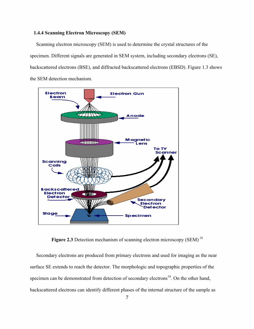
Scanning electron microscopy (SEM) is used to determine the crystal structures of the
specimen. Different signals are generated in SEM system, including secondary electrons (SE),
backscattered electrons (BSE), and diffracted backscattered electrons (EBSD). Figure 1.3 shows
the SEM detection mechanism.
Figure 2.3 Detection mechanism of scanning electron microscopy (SEM) 18
Secondary electrons are produced from primary electrons and used for imaging as the near
surface SE extends to reach the detector. The morphologic and topographic properties of the
specimen can be demonstrated from detection of secondary electrons18. On the other hand,
backscattered electrons can identify different phases of the internal structure of the sample as

8
they reveal the small variations of the atomic number on the sample surface by providing
different contrasts in image. These backscattered electron signals (BSEs) are widely used for the
investigation of specimen surface 20, 21. The mechanism of the interactions between incident
beam and sample surface are shown in Figure 2.3 18 .
1.4.4.1 SEM Images
Several SEM parameters should be adjusted in order to obtain a high quality image. One such
parameter is the working distance, which is known as the distance between the bottom pole piece
of the objective lens and the sample surface. The working distance affects depth of focus (D),
expressing the range of depth that an image appears to be in focus. The following equation is
used to determine the depth of field:
𝐷 = 2𝑟×𝑊𝐷/𝑅
Where 𝑟 is the maximum radius of the beam, 𝑊𝐷 represents the working distance, and 𝑅 is
the final aperture radius.
Using a lower accelerating voltage can be beneficial for obtaining good SEM image quality
and finer surface structure images. In contrast, applying higher accelerating voltages could
reduce the image contrast. The reason behind minimized contrast is the unnecessary signals from
the large penetration and diffusion area. Figure 1.4 shows the effects of accelerating voltage on a
sample composed of heavy or light elements 23.

9
Figure 1.4 Accelerating voltage effects on interaction of sample composed of heavy or light
elements 23

10
Chapter 2
Design and Fabrication of MIM Diode
2.1 Design and Fabrication of Pt-Al2o3-Al Metal-Insulator-Metal Diode
In this work, a Pt-Al2O3-Al metal-insulator-metal diode was fabricated to have high
asymmetry in I-V curve. The fabricated tunneling diode is intended to operate in the GHz
regime, and can also operate at higher frequencies (THz) by changing the dimensions. The
asymmetry of the I-V curve is reasonably very high due to a large difference in the work function
between Aluminum and Platinum metals.
2.1.1 Introduction
Investigation of new energy sources is vital because of the increasing demand for energy 3.
These new energy sources should be more efficient, cleaner, safer, and cheaper than traditional
energy sources. The solar energy based devices are clean and safe, but they are not efficient
enough, and at the same time they are expensive compared to fossil fuels and nuclear energy.
Efficiency of traditional solar cells is limited because of the band gap of semiconductors used in
these cells. This issue along with the huge amount of radiation received from the sun have led
researchers to investigate new technologies for converting solar energy to electricity. One
energy-harvesting device used in these systems is a rectifying antenna, also called a rectenna,
which converts solar radiation directly to electricity. The rectennas consist of an antenna, a
rectifier system, and frequency filters. The rectifier plays the primary role in converting AC

11
signals to direct current (DC), which can then be used directly or else used to charge batteries.
The cut-off frequency of the diode should be high enough to respond and be compatible with the
electromagnetic energy that is being harvested. Tunneling diodes are highly suitable for
rectification in microwaves and THz regimes (and beyond) because of their fast response time.
Metal-insulator-metal (MIM) diodes are one of the tunneling diodes used for rectification at high
frequencies 4.
MIM diode consists of two electrodes and a thin dielectric layer sandwiched in between the
electrodes 5. Although this type of diode is considered an optimum diode used in rectennas,
challenges remain in terms of its fabrication.
Rectennas consist of an antenna, filter circuits, and a rectifier diode. These devices have been
used for lower microwave frequencies; however, there is a growing interest in harvesting energy
in the infrared and optical frequency regimes 3, 5, 6, 7, 9. In this study, the fabrication process of
MIM diode will be discussed along with some challenges related to the fabrication process.
Some parameters including I-V characteristics, asymmetry, non-linearity, sensitivity,
coupling efficiency, and response time are important for determining the diode’s efficiency. The
current density highly depends on the work function of the metals, electron affinity of the
insulators, and thickness of the insulator layer. To have an efficient tunneling, the insulator layer
should be ultra-thin (less than 10 nm). Additionally, for operating a MIM diode at high
frequencies the contact area between the insulator and the metal interface should be very small;
i.e., the contact area at visible light range should be approximately 20 nm x 20 nm. It is very
difficult to have these ultra-small structures using current technology. In the next section, Pt-
Al2O3-Al metal-insulator-metal diode will be discussed.

12
2.1.2 Design and Fabrication
The area of the diode is an important parameter that determines the operation frequency of the
diode. The area and the frequency are related according to the following equations:
𝑓!= !!"!!!!
(1)
𝐶! =!!!!!!
! (2)
Where Ra is the antenna’s resistance, Cd is the diode capacitance, and Ad is the diode area 6, 10.
The design of this diode is a simple structure of four layers on top of the Si substrate. Ti, Pt, and
Al were the materials chosen for this diode.
For operation at 3GHz, the dimensions of the diodes were chosen to be 5 µm x 5 µm by using
Equations 1 and 2. The resulting Ra is 100Ω, which is close to a typical antenna resistance. The
thickness of the insulator was chosen to be 4 nm to have efficient tunneling. Although these
kinds of diodes are used for high frequency (near-IR or visible range), the frequency range was
not considered since the aim was to have high asymmetry in I-V curve.
Many processes were involved in the fabrication of the Pt- 𝐴l2𝑂3 -Al MIM diode including E-
beam evaporation, photolithography, reactive ion etching RIE, and Atomic Layer Deposition
(ALD) technique. The AFM was used to verify the smoothness of the surface of the diode and
the thickness of Al pads.

13
a)
b)
Figure 2.1 A schematic representation of the fabrication flow steps of the diode: a) Deposition of
Ti/Pt/Al2O3/Al; b) Patterning
The substrate of the diode was chosen to be a bare silicon wafer. The selected materials used
as the top and bottom electrodes were Platinum and Aluminum, respectively. These materials
were chosen due to their high difference in work function. They were good candidate metals for
the diode. The work function of Pt is 5.65 eV and that of Al is 4.28 eV. Electron-beam
evaporation was then used to deposit 50 nm of Ti onto the Si wafer in order to increase the

14
adhesion of the Pt layer to the substrate. Next, ultra thin layer (4 nm) of aluminum oxide (Al2O3)
was deposited onto the Pt layer using Oxford Plasma Lab 100 FlexAL ALD. It is preferred to
deposit insulators using ALD rather than oxygen plasma technique, as ALD is more precise and
controllable.
Figure 2.2 A schematic representation of the complete diode
Next, a 50 nm Al was deposited onto the insulator layer. Figure 2.1(a) shows the schematic of
the structure up until this step. A positive photoresist (S1813) was spin coated onto the ARC
under layer prior to photolithography. The conditions of the spin coating process were 2000
rounds per minute for 40 seconds followed by one minute soft baking at 110 ℃.
To carry out photolithography process, Karl Suss MA6 Mask Aligner was used. A glass
photo-mask with 5-micron diameter dots and 20 micron spacing was used to pattern the device,
as shown in Figure 2.1(b). The type of exposure was soft contact and G-line was chosen to
expose the substrate for five seconds. Following the development of the photoresist in AZ 300
MIF developer for one minute and etching the ARC by Reactive Ion Etching (RIE), Oxford
Instruments ICP380 plasma-based dry etching system was used to apply dry etching onto the Al

15
layer. A Laser End Point system connected to RIE was used to minimize the exposure of the
Platinum. The sample was then soaked in acetone in order to clean the photoresist on the top
followed by a four minute RIE process to clean the rest of the ARC by oxygen plasma. Figure
2.2 shows the final schematic of the device.
2.1.3 Results and Discussion
An important property of MIM diodes is the asymmetry in their I-V curve. This can be
achieved by having different metals in both sides of the insulator; however, this will result in a
high barrier asymmetric diode, which is good for having a large responsivity. Another property
of MIM diode is low resistance, which requires a low barrier height 1. A significant point that
needs to be considered prior to fabricating MIM diode is the selection of metals, since the work
function must be different to ensure asymmetrical and nonlinear characteristics of the diode. The
asymmetry can basically be described as the magnitude of the ratio of forward (IF) to reverse
bias (IR) current, as given by Equation 3.
FASYM=|𝐼!/𝐼! | (3)
Keithley 4200-SCS Semiconductor Characterization System, which was connected to a probe
station, was used to obtain current versus voltage (I-V) curve. One probe was connected to the
top of one of the Aluminum dots; another probe was connected to the Platinum surface. The
current was measured from -1 Volt to +1 Volt applied bias. As shown in Figure 2.3-a, the I-V
curve is highly asymmetrical. By using Equation 3, the asymmetry of the curve was plotted and
shown in Figure 2.3(b). The value of the asymmetry reaches approximately 240 when 1 Volt bias
is applied. A high asymmetric and non-linear I-V curve is illustrated in this study. However,

16
other parameters including tunneling efficiency, resistance, and responsivity should be
considered during design and fabrication of these diodes.
To achieve high responsivity at zero bias, the barrier heights of the electrodes should be high.
In our study, we used metals that have high work functions. Hence, the responsivity is also
expected to be high. To obtain efficient quantum tunneling, the insulating layer should be as thin
as possible; however, by using thick insulator layers, higher non-linearity can be achieved. To
achieve low resistance, the barrier heights of both sides should be low and the insulator layer
should be thin enough 11. However, there are always some trade-offs in this concept. By using a
thin insulator layer, a high non-linear and high asymmetric I-V curve was achieved in this study.
Figure 2.3 a) I-V curve; b) Asymmetry of Pt/Al2O3/Al MIM diodes
a)
b)

17
2.1.4 Conclusion
In this study, the fabrication of Pt-Al2O3-Al MIM diode was discussed in detail. In order to
increase the frequency of MIM diode operation, the capacitance values should be small. This can
be achieved either by increasing the thickness of the dielectric layer or by decreasing the contact
area. Therefore, in this work the thickness of the insulator layer was chosen to be 4nm. The
current-voltage characteristics of the fabricated diode are perceived to be sufficient for the diode
to work at the GHz regime. The value of the asymmetry was measured as approximately 240 at 1
Volt, which represents highly asymmetric and non-linear I-V curve as seen in Figure 2.3(a).
2.2 Comparison of the Effects of Various Materials Properties on Metal-Insulator-Metal
Diodes
This study compares various metal-insulator-metal diodes using the same bottom electrode
but different top electrodes. New metal-insulator-metal diodes were fabricated with four
insulators using various materials. Chromium was chosen for the bottom metal electrode while
Ti, Cr, Al, and Pt were chosen for the top metal electrode. This work indicates the effectiveness
of choosing the top metal for MIIIIM tunneling junction and its effect on the diode performance.
2.2.1 Introduction
The demand for using a sufficient and clean source of energy is continuous. Therefore,
investigation of a fast response time rectifying element is essential to overcome the issue of
having insufficient rectification1. The best candidate rectifying diode is metal-insulator-metal
diode due to its advantages over semiconductor solar cells in terms of response time7. Metal-

18
insulator-metal diode is a junction consisting of thin insulating layer (less than 10nm) between
two metals 1, 3, 6. Even though the architecture of this diode is simple, it is still a challenge to
determine which material’s properties are most suitable for producing the preferable electrical
performance of this device. Here, a comparison is provided of four different metal-insulator-
metal diodes with multi-layers of insulators by changing the top metal electrodes and keeping the
bottom one fixed. This comparison is based on the I-V characteristics and asymmetrical curves
of the fabricated diodes. Materials chosen for the top electrodes were Ti, Cr, Al, and Pt. I-V
characteristics are discussed in the next sections.
2.2.2 Experimental Details
Silicon oxide was the substrate chosen for all of the fabricated diodes to prevent the
conductivity of the substrate during electrical measurements. In fabrication of Cr-Tio2 -Al2o3 -Cr,
Cr-TiO2- Al2O3-Al, Cr-TiO2- Al2O3-Pt, Cr-TiO2- Al2O3-Ti MIIM diode, it was intended to keep
the first metal and insulator layers fixed while changing the second metal electrode. Chromium
was used as the fixed metal electrode, and chromium, aluminum, platinum, and titanium were
chosen for the second electrode. The substrate was cleaned by acetone and isopropanol alcohol
(IPA) and then dried by nitrogen blow. First, the negative photoresist (AznLOF 2035) was spin
coated onto the SiO2 substrate with 2000rpm spin speed for 40 sec, and then soft baking at 110°C
was applied to the sample for one minute to ensure that there were no remaining particles of
solvents. Following photoresist coating, Karl Suss MA6 Mask Aligner was used to pattern the
diode through photolithography process. The photo mask was designed with different structures
in different diameters. Following exposure, the substrate was baked at 110°C to allow for cross-

19
linking of the photoresist to occur. Next, the sample was developed by AZ300MIF developer for
one minute and rinsed by IPA followed by DI water for one minute and then dried with N2 gun.
Electron-beam evaporation technique was used to deposit 60nm of chromium. ALD technique
was utilized to deposit TiO2 and Al2O3, respectively. These two insulators were repeated in order
to obtain a total number of insulators of four. Each insulator was 0.75nm thick, giving a total of
3nm barrier thickness. In fact, using ALD is an effective way to deposit a uniform layer of
insulators due to its preciseness and controllability. Moreover, having a very uniform insulator is
good for current flow. Another photolithography step was applied to the same sample in order to
align the square’s structure and complete the whole device. The second metal was then deposited
with approximately 100nm thickness using electron-beam evaporation technique. The whole
device’s structure is clearly shown in Figure 2.4, and the overlapping area of metals one and two
is shown in Figures 2.5 and 2.6.
Figure 2.4 SEM image of the device structure showing three different sizes of the overlapping
area (30, 20, and 10 micron)

20
Figure 2.5 SEM image of the (Cr-TiO2- Al2O3-TiO2- Al2O3-Ti) diode structure
Figure 2.6 SEM image of the overlapping area (diode active area)

21
2.2.3 Results and Discussion
In order for MIM diodes to have optimal behaviour, the insulator layer requires a low surface
roughness, uniform thickness, and stoichiometry. This can be obtained by having a small device
area (in the order of 𝜇𝑚! or less) 4. Four combinations of MIM diode with different work
function Δ φ (= φ 2 – φ 1) values were fabricated and characterized. The work function of
chromium as the base metal is 4.5eV(φ1). To improve the device’s performance, a quadra
insulator diode was fabricated using repeated TiO2 and Al2O3 insulator layers. The same quadra
insulator diode was repeated but with the second metal changed in order to study the difference
between different material properties on the metal-insulator-metal diode. Each insulator layer of
this quadra insulator layer diode was 0.75nm thick. These insulators were deposited by using
ALD at a rate of 0.105 ± 0.001 nm/cycle for Al2O3 and a rate of 0.0437 ± 0.001 nm/cycle for
TiO2.
Figure. 2.7 shows the current-voltage electrical response for all the fabricated diodes having
doubled insulator (red curve) and four insulators (blue curve). It is clearly shown that current
resulted from diodes with four insulators is much larger than that of two insulators. When the
device is forward biased, the electrons tunnel via the aid of a quantum well formed due to the
insulator barrier, however, when a reverse biase is applied there is no quantum well formation
occur and thus electrons must tunnel through all barriers without any assistance2. Therefore a
highly nonlinear and asymmetric I-V curve results. Since there is a trade off between
conductivity and nonlinearity, it is hard to achieve both, and hence devices with two insulators
exhibited more nonlinear curves however conductivity is higher for devices with four insulators
as shown in figure 3. From this figure also, it is clear that the MIM diodes using Ti and Cr, and

22
Pt as top electrodes perform most asymmetric diodes. This could be attributed to their band
energy offset at the interface, which affects the tunneling current through insulating layers.
FIG.3. The I-V characteristics curve of the a) Cr-I1I2I1I2 -Ti and Cr-I1I2-Ti , b) Cr- I1I2I1I2 -
Cr and Cr- I1I2-Cr, c) Cr- I1I2I1I2-Al and Cr- I1I2-Al, and d) Cr- I1I2I1I2-Pt and Cr- I1I2-Pt diode.
Figure.2.8 compares the asymmetry curve of MIIIIM / MIIM fabricated diodes when a
voltage range of (0.5-3 volts) is applied to these devices. . As can be seen from this figure the
highest asymmetry value (40) was achieved at a voltage value of 1volt when using Ti as top
electrode for the MIIIIM structure (blue curve), but for MIIM structure (red curve) it shows less
asymmetry. When using the Pt as top electrode the asymmetry was calculated as 6 under 0.5
voltage, and much less (about 1) for CrIIPt .For the device using Cr for both metal electrodes and
with four layer of insulators, the I-V curve was highly asymmetric with value of 16 under
voltage of 2volts. Even though this diode consists of the same metal electrodes (Cr), there is still

23
a work function difference between the two electrodes. The reason of such low barrier height on
one side might be due to the difference in processing conditions of electrodes s, as explained by
Hobbs 5. The forward current, which is defined as those electron tunneled from top electrode to
the base electrode (Cr), was larger than the reverse current, which is those electrons tunneled
from base electrode to top electrode, and hence there is inherent work function difference. Since
asymmetry of MIM diode is a function of applied voltage, the amount of voltage bias affects the
resulted asymmetry values. Figure.2.8 also shows a low asymmetry using a combination of Cr
and Al as base and top electrode, respectively especially for MIIIIM structures at voltage of 1
volt. By applying a voltage bias to Al electrons of the Al tunneled through the thin barrier with a
total thickness of 3nm. The amplitude of the current obtained from Cr electrode depends on the
barrier heights as well as on the applied voltage. It can be concluded that the increase in
asymmetry is not linear function of the work function difference between base and top electrodes
which is in good agreement with other studies2.
! !! !!!!!!!!!!!!!!!!!!!
!! !! !

24
Figure 2.8 Asymmetry curve of the fabricated diodes indicating the two structures MIIM
and MIIIIM.
The barrier heights of device’s interface were calculated for difference fabricated diodes
and were reported in table.1 The electron affinity of 0.75 nm thickness of the TiO2 and Al2O3
was reported as 4.3 eV, and 3.5 eV, respectively. Since each diodes have five interfaces, the
barrier heights were calculated as follow: Φ1 = φ1 – χ1 = eV, Φ2 = Φ3 = Φ4 = χ1 – χ2 , and Φ5 = φ2
– χ2.
Table.1 Barrier height potential of fabricated MI1I2I1I2M diodes.
MIM# Φ1=ϕ1-χ1(ev) Φ2=Φ3=Φ4= χ 1-χ2(ev) Φ5= ϕ2-χ2(ev) 1 0.2 0.8 0.83 2 0.2 0.8 1 3 0.2 0.8 0.78 4 0.2 0.8 2.15
Table.2 shows the list of MIIIIM diodes’ various combinations and the differences in work
function values between metals one and two. The study of different materials’ properties is
crucial to determine the suitable material combinations for the optimum metal-insulator-metal
diode operation performance.
Table.2 MIIIIM diode combinations and their difference in work function values reported in this
study
Metal 1-Insulator 1, 2, 3, 4 –Metal 2 configuration
Work function difference value Δ φ (= φ 2 – φ 1)
Cr-Tio2- Al2o3-Tio2 -Al2o3 -Ti -‐0.17eV Cr-Tio2- Al2o3-Tio2 - Al2o3 - Cr >0eV Cr-Tio2- Al2o3-Tio2 - Al2o3 -Al -‐0.22eV Cr-Tio2- Al2o3-Tio2 - Al2o3 - Pt 1.15eV

25
2.2.4 Conclusion
In this work, four new MI1I2I3I4M diodes were compared following successful fabrication.
Characterization of these various diodes was achieved from their I-V electrical responses.
MIIIIM diodes using Ti and Cr, and Pt as the second metal electrode exhibited superior
performance in terms of asymmetry, while a combination of (Cr –Al) shows relatively lower
asymmetry curve.

26
Chapter 3
Electron Beam Lithography
3.1 Overview of Electron Beam Lithography
Electron beam lithography (EBL) is popular due to its excellent resolution capability,
significant reliability, and ability to write reproducible structures over large areas, and low cost.
EBL is capable of achieving sub-10nm resolution patterns 17. EBL, which was generated from
scanning electron microscopy (SEM), is a mask less lithography technique since it is only based
on the electron beam source. Because electron beam has a small wavelength and small probe
size, Electron Beam Lithography has become the most useful nanofabrication tool.
The spot size of electron beam can be less than 5nm, and the beam can be focused using
electron optics. However, the literature has reported the general capabilities of different direct
lithographies such as (~10 nm) for EBL.
Table 3. Capabilities of different direct nanofabrication techniques 19
Technology Capability
Optical lithography
~30 nm
Electron beam lithography
~10 nm
Nanoimprint lithography
~10 nm
Scanning probe lithography
~1 nm
Focused ion beam ~30 nm
By using de Broglie wavelength equation, one can estimate the electron wavelength.

27
EBL system can resolve a minimum feature size depending on many factors such as resist type,
resist thickness, exposure dosage, beam current level, development process, proximity
correction, and resistance to etching of the used EBL resist.
3.2 Electron Beam Lithography Systems, Operation, and Working Scheme
3.2.1 Electron Beam Lithography Systems
EBL has different types of systems that have been developed which are used for both research
and industry. A schematic of an EBL system is shown in Figure 3.1. Generally, a beam of
electrons is deflected to a desired area in the substrate surface. This electron beam modifies the
resist depending on its tone by blanking the beam, moving it to another location, and then turning
it on in order to expose the resist again. By repeating this process the desired pattern is achieved.

28
Figure 3.1 EBL System based on SEM 22
Even though sub-10 nm resolution is achieved by EBL, exposures are done serially which reduces
throughput and also limits to the scientific research applications.
Two different types of EBL systems are used for EBL writing: raster and vector scan. In raster scan the
electron beam is scanned in only one direction and a mechanical translation of the stage occurs in the
perpendicular direction. Unlike raster scan, in vector scan the electron beam is scanned in both x and y
directions with beam blanking. Here the pattern writing will be pixel by pixel and without stage movement
within each writing field, yet the stage or the substrate will move to the next location after each writing field.

29
3.2.2 Working Scheme of EBL
An electron beam scans a substrate surface covered with a resist material. This resist
material is sensitive to electrons, and is chemically modified depending on its tone.
There are two different tones of EBL resists: positive and negative. The positive tone
resist is dissolved during the development process, while the negative resist remains, as
shown in Figure 3.2.
Figure 3.2 A schematic illustration of EBL working scheme
3.3 Proximity Effect
Scattering of the electron beam during exposure leads to pattern distortion. The
incident electrons on the resist film cause the resist molecules chains to break.

30
During the development process, the exposed areas will be dissolvable. When
electrons expose undesired areas of the resist, this is called proximity effect. Two
scattering events occur: forward scattering and backscattering. In forward scattering
event, primary electrons generate secondary electrons along its path but with low
energy. However, in backscattering event the resist is exposed far from incidence
(proximity effect), because secondary electrons with higher energy and long travel
length are generated along backscattered electron path that can expose the resist
there.
3.3.1 How to Reduce Proximity Effect
Using thinner resist can minimize the forward scattering. Moreover higher applied
voltage can also be used to reduce proximity effect. If it is possible, choosing a
substrate with smaller atomic mass unit can be useful. In addition, commercial
software can be used to correct the proximity effect by producing a dose-corrected
fractured data file.

31
Chapter 4
Gray Scale Lithography
4.1. Motivation
The second half of this thesis attempts to engineer the contrast curve of electron-beam
lithography resist (polystyrene) with a great freedom by using multi-layer of polystyrene. By using
multi-layer resist stack, an additional degree of tuning the overall contrast curve is offered.
Successfully designing the resist stack of polystyrene with higher contrast allows it to be used
for the fabrication of multi-level zone-plate/Fresnel lens.
4.2. Overview of Gray Scale Lithography
In EBL, resist properties are characterized by sensitivity and contrast which can be derived from
its contrast curve. To a certain degree, resist sensitivity and contrast can be tailored by experimental
parameters. For example, for positive resist such as PMMA, using lower electron beam energy can
increase the sensitivity or stronger concentration of the developer (e.g. MIBK:IPA=1:1, instead of
1:3) and increase the development temperature or the development time. The dependence of
contrast on those parameters is not obvious, but for typical resist increased sensitivity is always
accompanied by decreased contrast. Nonetheless, the tailoring of the contrast curve using single
resist layer is limited. It is proposed that by using polystyrene with different molecular weights

32
(Mw), a multi-layer resist stack can be designed in order to engineer the contrast curve of the stack
with great freedom.
Polystyrene is chosen because its sensitivity is proportional to its Mw 12, 14, which is
commercially available from ~1 kg/mol up to 2000 kg/mol. Moreover, it is not necessary to have
polystyrene with many different Mw, as one can “simulate” an arbitrary Mw (actually should be
Mn, number averaged molecular weight, which is more important than weight averaged molecular
weight Mw) by mixing two polystyrenes with very different Mw 15. As shown schematically in
Figure 4.4, if the resist layers have very high contrast - which is the case for low Mw range
polystyrene - and the sensitivity of the layers differ greatly from each other, a contrast curve with
roughly a stair-case shape may be achieved, which is ideal for the fabrication of multi-level zone-
plate/Fresnel lens 16.
Figure 4.1 Chemical structure of Polystyrene

33
Figure 4.2 Schematic of contrast curves of five high contrasts resists having decreasing
sensitivity, as well as the contrast curve for the stack of the five resists (most sensitive on bottom
and least sensitive on top)
Substrate
Resist 1
Resist 2
Resist 3
Resist 4
Resist 5

34
4.3. Experimental
4.3.1 Doubled-layer Resist Stack
In the experiment, two PS samples with Mw of 50 kg/mol and 4.5 kg/mol were used. Two
grams of PS of Mw of 50 kg/mol were dissolved in 100ml toluene solvent. Another 2g of PS of
Mw of 4.5 kg/mol were dissolved in 100ml toluene solvent. A third solution of 22 kg/mol was
prepared by mixing the previous two samples of 50 and 4.5 kg/mol. Spin coating of 50 kg/mol
solution was applied on bare Si wafer, and 22 kg/mol solution was spin coated on another Si
wafer. Before exposure, the films were baked for one minute for hardening after the spin coating
step. Dektak-8 program was used to check the thickness of the two films. The pattern was
exposed at 20kev and 320 PA beam current and developed using xylene for one minute. After
development, the remaining thickness was measured by AFM.
A straightforward way to generate the resist stack is by spin coating the polystyrene layer by
layer. However, this has not yet been successful because it was found that the solvent dissolved
the previous layers during the coating of a new layer. It is known that double-layer PMMA can
be spin coated; thus, the same may be possible for polystyrene if a suitable solvent or mixture of
solvents can be identified. As proof of concept, a double layer of polystyrene was obtained by
thermally bonding one layer to the other, with the first layer spin coated on a bare silicon wafer
and the second layer spin coated on an anti-adhesion treated wafer, as shown in Figure 4.3.

35
Figure 4.3 A schematic representation of thermal bonding of Ps layers
The contrast curve of two-layer stack, 22 kg/mol on top of 50 kg/mol, is shown in Figure 4.4.
Here the effective 22 kg/mol is simulated by a mixture of 50 kg/mol and 4.5-kg/mol polystyrene.
Due to the small difference between the two Mw, the contrast curve has a continuous and smooth
slope, yet the contrast is decreased to 2.0 which is lower than the single layer resist with similar
Mw (γ~3.0).
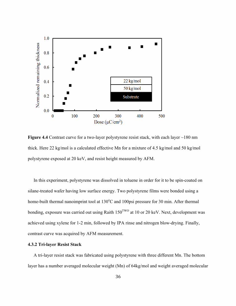
36
Figure 4.4 Contrast curve for a two-layer polystyrene resist stack, with each layer ~180 nm
thick. Here 22 kg/mol is a calculated effective Mn for a mixture of 4.5 kg/mol and 50 kg/mol
polystyrene exposed at 20 keV, and resist height measured by AFM.
In this experiment, polystyrene was dissolved in toluene in order for it to be spin-coated on
silane-treated wafer having low surface energy. Two polystyrene films were bonded using a
home-built thermal nanoimprint tool at 130oC and 100psi pressure for 30 min. After thermal
bonding, exposure was carried out using Raith 150TWO at 10 or 20 keV. Next, development was
achieved using xylene for 1-2 min, followed by IPA rinse and nitrogen blow-drying. Finally,
contrast curve was acquired by AFM measurement.
4.3.2 Tri-layer Resist Stack
A tri-layer resist stack was fabricated using polystyrene with three different Mn. The bottom
layer has a number averaged molecular weight (Mn) of 64kg/mol and weight averaged molecular
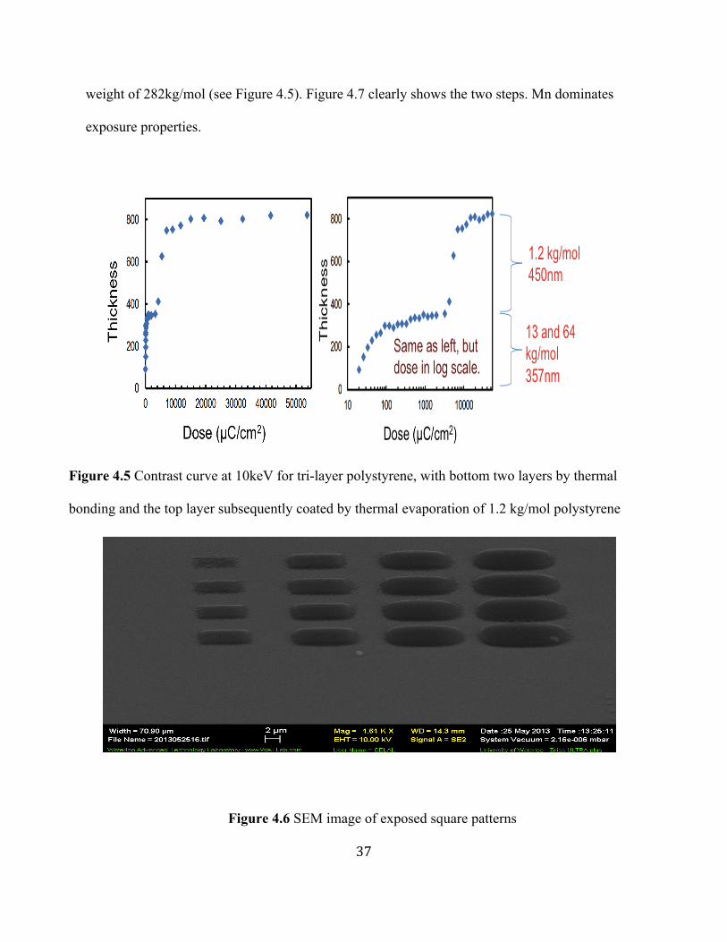
37
weight of 282kg/mol (see Figure 4.5). Figure 4.7 clearly shows the two steps. Mn dominates
exposure properties.
Figure 4.5 Contrast curve at 10keV for tri-layer polystyrene, with bottom two layers by thermal
bonding and the top layer subsequently coated by thermal evaporation of 1.2 kg/mol polystyrene
Figure 4.6 SEM image of exposed square patterns

38
Figure 4.7 SEM and AFM images of exposed square patterns which clearly show the two steps.
The square is 3.5µm in the CAD file. The larger square for the bottom two layers is due to
proximity over-exposure.
To validate the results, a four-layer stack of polystyrene was achieved using thermal bonding
technique. First, polystyrene with different numbers of averaged molecular weight was dissolved
in toluene. Each polystyrene film had a thickness of 200-300nm. The first polystyrene film with
Mn of 170 kg/mol was spin coated on a bare Si wafer, while the second film with Mn of 64
kg/mol was spin coated onto a PEN sheet coated with a fluorocarbon film. The two polystyrene
films were bonded using a home-built thermal nanoimprint tool at 130oC and 100psi pressure for
30 min. Reactive ion etching RIE was used to coat fluorocarbon film on PEN sheet in order to
facilitate the separation of the two polystyrene films after bonding. By repeating the process of
spin coating and thermal bonding using polystyrene films with Mn of 18 kg/mol and 6 kg/mol,
one can achieve four layers of polystyrene with different weight averaged molecular weight
(Figure 4.8). Exposure was carried out using Raith 150TWO at 20 keV. Next, development was

39
achieved using xylene for 3 min followed by IPA rinse and nitrogen blow-drying. Finally,
contrast curve was acquired by AFM measurement, as shown in Figure 4.10.
Figure 4.8 Schematic representation of thermal bonding process of the four polystyrene films
where weight averaged molecular weight is in the following order: (Mw1>Mw2>Mw3>Mw4)

40
Figure 4.9 SEM images of the exposed square patterns showing the height of the resist
corresponding to the film thickness

41
Figure 4.10 Contrast curve of the four-layer resist stack using polystyrene as negative resist
4.5 Fresnel Lenses
A Fresnel lens is a thin light magnifier that can be used as an alternative to the conventional
continuous surface lens. Augustin Jean Fresnel developed this type of lens in the early 1800s. Due
to its structure that becomes flat in one side and ridged on the other, Fresnel lens is cost effective,
with much of the optical material removed and the surface curvature still being maintained. This
concept is illustrated in Figure 4.11.
0
200
400
600
800
1000
1200
1400
1 10 100 1000 10000
Thickness (nm)
Dose (μC/cm2 )

42
Figure 4.11 Conceptual illustration (in side-profile) of collapsing a continuous surface
aspheric lens into an equivalent power Fresnel lens 18

43
Appendix
List of Publications
Papers
1. M. Alhazmi, M. Yavuz and B. Cui, Contrast curve engineering by using multi-layer polystyrene
electron beam resist, 57th International Conference on Electron, Ion and Photon Beam
Technology and Nano-fabrication (EIPBN), Nashville, May 2013.
2. M. Alhazmi, F. Aydinoglu, B. Cui, O. M. Ramahi, M. Irannejad, A. Brzezinski and M. Yavuz,
"Comparison of various materials properties effect on metal-insulator-metal diodes", under
preparation for submission.
3. F. Aydinoglu, M. Alhazmi, S, Alqarni, B. Cui, O.M. Ramahi, M. Yavuz, Design and fabrication
of pt-al2o3-al metal-insulator-metal diode, 24th Canadian Congress of Applied Mechanics
(CANCAM), Saskatoon, SK, Canada, 2nd June, 2013.
4. C. Con, M. Alhazmi, M. yavuz and B. cui, freeze-drying for the reduction of e-beam resist
collapse, MNE conference in London (UK), September 2013
5. F. Aydinoglu, M. Alhazmi, B. Cui, O. M. Ramahi, M. Yavuz, "Higher Performance Metal-
Insulator-Metal Diodes using Multiple Insulator Layers" Applied Physics Letters (under review,
Sep 2013.

44
Conference presentations
1- M. Alhazmi, M. Yavuz and B. Cui, Contrast curve engineering by using multi-layer
polystyrene electron beam resist, 57th International Conference on Electron, Ion and Photon
Beam Technology and Nano-fabrication (EIPBN), Nashville, May 2013.
2- F. Aydinoglu, M. Alhazmi, S, Alqarni, B. Cui, O.M. Ramahi, M. Yavuz, Design and
fabrication of pt-al2o3-al metal-insulator-metal diode, 24th Canadian Congress of Applied
Mechanics (CANCAM), Saskatoon, SK, Canada, 2nd June, 2013.

45
Bibliography
[1] Eliasson, B. 2001, “Metal –Insulator-Metal diodes for solar energy conversion”, University of
Colorado, Boulder, Doctoral thesis.
[2] B. H. Strassner and K. Chang.2005, “Rectifying antennas (rectennas),” in
Encyclopedia of RF and Microwave Engineering. Hoboken, NJ: Wiley, p. 4418.
[3] Grover, S., Moddel, G. 2011, "Applicability of Metal/Insulator/Metal (MIM) Diodes to Solar
Rectennas", IEEE Journal of Photovoltaics, Vol.1 (1), pp.78-83.
[4] Da Costa V., Romeo, M., Bardou, F. 2003, "Statistical properties of currents flowing through
tunnel junctions", Journal of Magnetism and Magnetic Materials, Vol.258–259, pp. 90-95.
[5] Grover, S., Dmitriyeva, O., Estes, M.J., Moddel, G. 2010, "Traveling-Wave
Metal/Insulator/Metal Diodes for Improved Infrared Bandwidth and Efficiency of Antenna-
Coupled Rectifiers", IEEE Transactions on Nanotechnology, Vol.9 (6), pp. 716-722.
[6] Choi, K., Dagenais, M., Peckerar, M. 2009, “Fabrication of Thin Film Asymmetric Tunneling
Diode using Geometric Field. Enhancement”, Semiconductor Device Research Symposium,
ISDRS '09. International, College Park, MD, USA.
[7] Krishnan, S., La Rosa, H., Stefanakos, E., Bhansali, S., Buckle K. 2008, "Design and
development of batch fabricatable metal–insulator–metal diode and microstrip slot antenna as
rectenna elements”, Sensors and Actuators A: Physical, Vol.142 (10), pp. 40-47.

46
[8] Dagenais, M., Choi, K., Yesilkoy, F., Chryssis, A., Peckerar, M. 2010, "Solar spectrum
rectification using nano-antennas and tunneling diodes", Optoelectronic Integrated Circuits XII.
Edited by Eldada, Louay A. Lee, El-Hang. Proceedings of the SPIE, Vol.7605, pp. 76050E-
76050E-12.
[9] Krishnan, S., 2004 “Design, Fabrication and Characterization of Thin-Film M-I-M Diodes for
Rectenna Array", University of South Florida, Florida, Master Thesis.
[10] S., Stefanakos, E., Bhansali, S. 2008, “Effect of dielectric thickness and contact area on
current-voltage characteristics of thin film metal-
[11] Hashem, I.E.; Rafat, N.H.; Soliman, E.A., 2013, "Theoretical Study of Metal-Insulator-
Metal Tunneling Diode Figures of Merit", IEEE Journal of Quantum Electronics, Vol.49 (1), pp.
72-79.
[12] H. Y. Ku and L. C. Scala, J. Electrochem, 1969,Soc., 116, 980.
[13] C. Con, R. K. Dey, M. Ferguson, J. Zhang, R. Mansour, M. Yavuz and B. Cui, 2012,
Microelectron. Eng., 98, 254.
[14] S. Ma, C. Con, M. Yavuz and B. Cui, 2011, Nanoscale Research Letters, 6, 446.
[15] R. K. Dey and B. Cui, presented at EIPBN 2012, and manuscript submitted.
[16] E. D. Fabrizio, F. Romanato, N, Gentili, S. Cabrini, B. Kaulich, J. Susini and R. Barrett,
1999, Nature, 401, 895.
[17] Grigorescu, A. E. and Hagen, C. W. 2009. Resists for sub-20-nm electron beam
lithography with a focus on HSQ: state of the art. Nanotechnology, 20, 292001
47
[18] P. University. Scanning Electron Microscope.Accessed on September 10th,2013.
http://www.purdue.edu/rem/rs/sem.htm
[19] Cui, Z. (2008). Nanofabrication. doi: 10.1007/978-0-387-75577-9
[20] L. Reimer and C. Tollkamp, 1980,"Measuring the Backscattering Coefficient and Secondary-
Electron Yield inside a Scanning Electron-Microscope," Scanning, vol. 3, pp. 35-39.
[21] G. Messina, A. Paoletti, S. Santangelo, and A. Tucciarone,Feb 1995, "A Single Quality Factor
for Electron Backscattering from Thin-Films," Microelectronic Engineering, vol. 27, pp. 183-
186.
[22] Shuhua, W., Lan, D., & Jing, Z. 2013, Realization and application of nanometer E-beam
lithography system. IEEE 5th International Nanoelectronics Conference (INEC), (5), 164–167.
doi: 10.1109/INEC.2013.6465985.
[23] J. Y. Liu, 2000."High-resolution and low-voltage FE-SEM imaging and microanalysis in
materials characterization," Materials Characterization, vol. 44, pp. 353-363.