Embed Size (px)
Citation preview

Fabrication and Characterization of Electrodeposited Bismuth TellurideFilms and Nanowires
Cheng-Lung Chen,†,‡ Yang-Yuan Chen,*,‡ Su-Jien Lin,*,† James C. Ho,‡,§ Ping-Chung Lee,‡
Chii-Dong Chen,‡ and Sergey R. Harutyunyan‡,|
Department of Materials Science and Engineering, National Tsing Hua UniVersity, Hsinchu, Taiwan,Republic of China, Institute of Physics, Academia Sinica, Taipei, Taiwan, Republic of China, andInstitute for Physical Research, NAS, Ashtarak-2, Armenia
ReceiVed: October 16, 2009; ReVised Manuscript ReceiVed: January 25, 2010
To elucidate low-dimensional effects on thermoelectric materials, bismuth telluride film and nanowires arraywere fabricated by potentiostatically electrodeposition. Both materials are slightly Te-rich, n-type Bi2Te3,exhibiting preferred orientation in rhombohedral strcture. For both the Seebeck coefficient S ≈ -70 µV/K at300 K decreases linearly with decreasing temperature, showing a diffusive nature of current flow. Thetemperature dependence of resistivity ()1/σ) of nanowires obtained from the data of a nanowires array anda single-nanowire reveals a better electric conductivity than that of the bulk. By coupling temperature-dependentthermal diffusivity and heat capacity data with a modified effective medium theory, a thermal conductivityκ of 0.75 W/(m K) was obtained at 300 K. The ZT was calculated to be 0.45 at 300 K and 0.9 at 350 K forBi2Te3 nanowires.
1. Introduction
Thermoelectric (TE) materials are capable of convertingthermal energy directly into electrical energy or vice versa, asbeing demonstrated in power generation or refrigeration.However, low efficiency has limited their use only in nichemarkets.1,2 The efficiency of a thermoelectric material isconventionally judged by its dimensionless figure of merit,
where T, S, σ, and κ are respectively the absolute temperature,Seebeck coefficient, electrical conductivity, and thermal con-ductivity.3 The compound parameter, σS2, is often referred toas the power factor. Accordingly, an ideal TE material shouldpossess high Seebeck coefficient, high electrical conductivity,but low thermal conductivity, a requirement not easily met. Overthe years, bismuth telluride, Bi2Te3, has been recognized as thebest TE material with the highest ZT ≈ 1 near ambienttemperature.4 To enhance future applications, the ZT value needsto be further raised considerably. A seemingly viable approachis reduction of dimensionality. For example, a ZT enhancementmainly due to thermal conductivity reduction, through phonon-blocking and electron-transmitting, in superlattices was reportedby Venkatasubramanian et al.5 Much higher ZT values wereeven predicted theoretically by Hicks and Dresselhaus for one-dimensional, nanowidth wires, based on the change of electronicdensity-of-states and increased phonon surface scattering.6 Thiswork is, therefore, carried out as part of our targeted efforts toelucidate low-dimensional effects on S, σ, and κ.
Many techniques including coevaporation, molecular-beamepitaxy, and metal-organic chemical vapor deposition have
been developed to grow Bi2Te3 films.7-9 Even though they arecapable of producing good quality films, the high fabricationcost and toxic precursors make them impractical in large scaleproduction. An alternative method is chemical electrodeposition,which is also applicable to fabricate nanowires in prepatternedtemplates.10,11 Nanoporous membranes such as anodized alu-minum matrix (AAM) can be used as the template material,since they are particularly suitable for preparing high aspectratio structures. Due to its inherent advantages of simplicity,rapidity, and cost-effectiveness, this method has been extensivelyapplied to many thermoelectric materials including some basedon bismuth telluride.12-15 Even so, a comprehensive understand-ing of thermoelectric properties at low dimensions remains asthe ultimate goal in obtaining high ZT materials.
While certain growth conditions for films have been reportedrecently,16 thermoelectric transport property data are somewhatlimited. In this respect, fabricating a thermoelectric device basedon nanowires is even more an arduous task, considering thedissonant gap between synthesis and thermoelectric character-ization of the product. Furthermore, most of the electrodepositionbaths were developed first for thin films and then demonstratedfor nanowires by filling the nanoporous membrane. In thisarticle, we present a systematic study of potentiostaticallyelectrodeposited Bi2Te3 films and nanowires embedded in AAM.Electrical resistivity and Seebeck coefficient were directlymeasured. An indirect but viable approach is introduced toconveniently characterize thermal conductivity of nanowires.This was done by coupling experimentally determined thermaldiffusivity and heat capacity data with a modified effectivemedium theory. Finally, the individual parameters S, σ, and κ
together result in estimated ZT values.
2. Experimental Section
Bi2Te3 films were electrodeposited potentiostatically at -150mV onto an ITO glass substrate from 1 M HNO3 solutioncontaining 0.008 M Bi3+ and 0.014 M HTeO2
+. The overallchemical reaction can be described as17
* To whom correspondence should be addressed. E-mail:[email protected] (Y.Y.C.) and [email protected] (S. J. L.).
† National Tsing Hua University.‡ Academia Sinica, Taipei.§ On leave from Wichita State University, Wichita, Kansas.| Institute for Physical Research, NAS.
Τ ) σS2T/κ (1)
J. Phys. Chem. C 2010, 114, 3385–3389 3385
10.1021/jp909926z 2010 American Chemical SocietyPublished on Web 02/08/2010
The process was carried out in a conventional three-electrodecell with a saturated calomel electrode as the reference and aplatinum sheet as the counter electrode. To remove oxygen fromsolution, argon was bubbled into the electrolyte throughout theexperiment. After electrodeposition, as-prepared Bi2Te3 filmswere annealed in argon with 5% H2 at 523 K for 2 h.
The AAM template was produced in a two-step anodizedprocess.18 An aluminum foil with purity 99.999% and thickness0.13 mm (Alfa Aesar) was anodized in acid solutions, yieldingan array of densely packed, hexagonally arranged, parallelnanochannels. The channel diameter can be systematicallycontrolled by anodized voltage, type of electrolyte, and bathtemperature. After anodization, the remaining aluminum layerwas removed by CuCl2 solution. A subsequent etching treatmentby 0.5 M NaOH aqueous solution for 7-10 min was carriedout to remove the barrier layer on the bottom side, followed bydepositing a gold-film layer to serve as a conductive electrode.
By filling the template, a Bi2Te3 nanowires array was thenfabricated with similar growth conditions, rinsed with deionizedwater, and dried in nitrogen. A thin gold film (∼300 nm) wasthermally evaporated onto the top surface for oxidation preven-tion. It has been suggested that annealing treatment to nanowireswould improve their thermoelectric properties.19 In our experi-ence, annealing lowers electrical resistivity of as-prepared filmas expected, but the annealing-induced thermal shock leads toextremely high electrical resistance in nanowires embedded inAAM. Therefore, experimental data and analysis were confinedto Bi2Te3 bulk, annealed films, and as-prepared nanowires. Toobtain individual nanowires, AAM was dissolved in 2 M NaOHaqueous solution, then washed by deionized water and centri-fuged to remove residual NaOH thoroughly. Separated Bi2Te3
nanowires were dispersed in ethanol, ready for measurements.For comparison with films and nanowires, a Bi2Te3 bulk was
prepared by the Bridgeman method. Briefly, high-purity(99.999%) bismuth and tellurium powers were mixed in theappropriate molar ratio and sealed in a quartz tube, which wasevacuated to 10-5 Torr, kept in a furnace at 1073 K for 12 h,and then cooled to room temperature in 1 day.
A 3-KW diffractometer (Philips) equipped with an arraydetector based on real time multiple strip was employed forcrystal structural characterization. Morphologies of films andnanowires array were determined by a field emission scanningelectron microscope (SEM, Hitachi S-4200), and compositionsby energy dispersive X-ray. Transmission electron micrographs(TEM) and diffraction patterns were obtained with a fieldemission transmission electron microscope operated at 200 kV(JEOL JEM-2100).
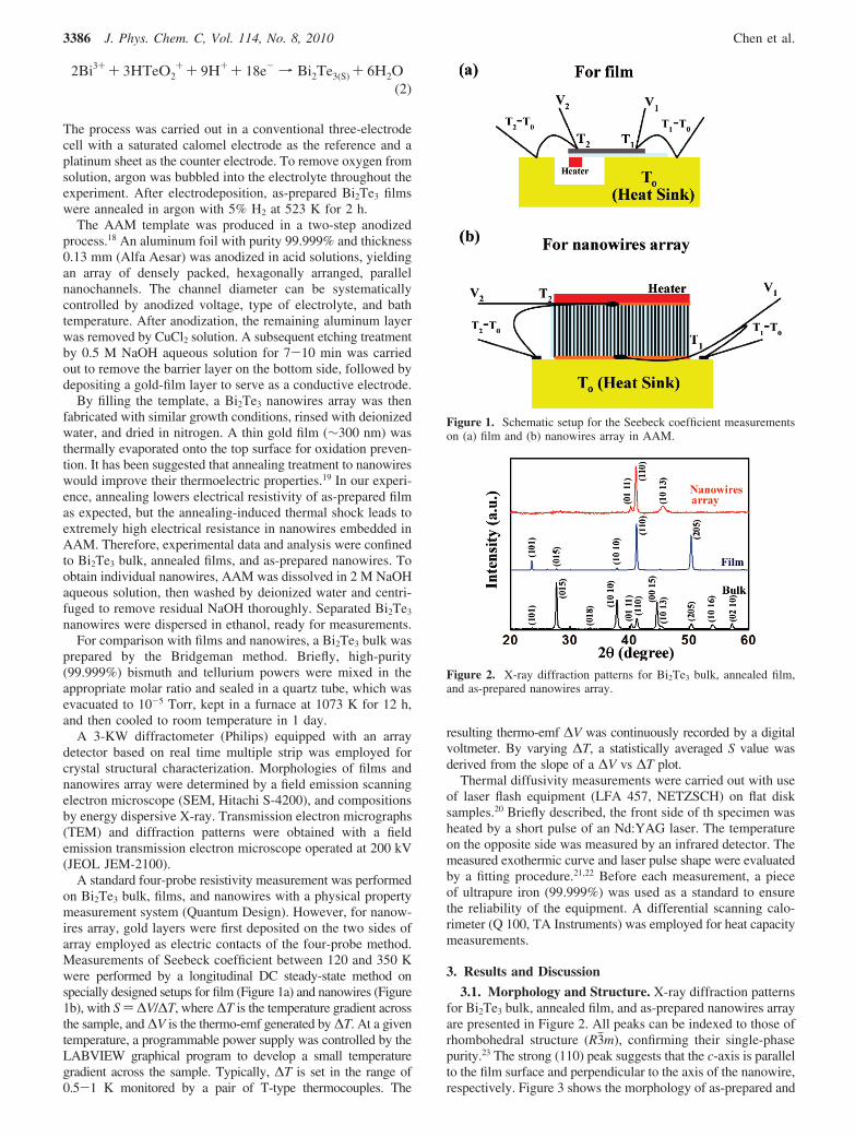
A standard four-probe resistivity measurement was performedon Bi2Te3 bulk, films, and nanowires with a physical propertymeasurement system (Quantum Design). However, for nanow-ires array, gold layers were first deposited on the two sides ofarray employed as electric contacts of the four-probe method.Measurements of Seebeck coefficient between 120 and 350 Kwere performed by a longitudinal DC steady-state method onspecially designed setups for film (Figure 1a) and nanowires (Figure1b), with S ) ∆V/∆T, where ∆T is the temperature gradient acrossthe sample, and ∆V is the thermo-emf generated by ∆T. At a giventemperature, a programmable power supply was controlled by theLABVIEW graphical program to develop a small temperaturegradient across the sample. Typically, ∆T is set in the range of0.5-1 K monitored by a pair of T-type thermocouples. The
resulting thermo-emf ∆V was continuously recorded by a digitalvoltmeter. By varying ∆T, a statistically averaged S value wasderived from the slope of a ∆V vs ∆T plot.
Thermal diffusivity measurements were carried out with useof laser flash equipment (LFA 457, NETZSCH) on flat disksamples.20 Briefly described, the front side of th specimen washeated by a short pulse of an Nd:YAG laser. The temperatureon the opposite side was measured by an infrared detector. Themeasured exothermic curve and laser pulse shape were evaluatedby a fitting procedure.21,22 Before each measurement, a pieceof ultrapure iron (99.999%) was used as a standard to ensurethe reliability of the equipment. A differential scanning calo-rimeter (Q 100, TA Instruments) was employed for heat capacitymeasurements.
3. Results and Discussion
3.1. Morphology and Structure. X-ray diffraction patternsfor Bi2Te3 bulk, annealed film, and as-prepared nanowires arrayare presented in Figure 2. All peaks can be indexed to those ofrhombohedral structure (R3jm), confirming their single-phasepurity.23 The strong (110) peak suggests that the c-axis is parallelto the film surface and perpendicular to the axis of the nanowire,respectively. Figure 3 shows the morphology of as-prepared and
2Βi3+ + 3ΗΤe2+ + 9Η+ + 18e- f Βi2Τe3(S) + 6Η2
(2)
Figure 1. Schematic setup for the Seebeck coefficient measurementson (a) film and (b) nanowires array in AAM.
Figure 2. X-ray diffraction patterns for Bi2Te3 bulk, annealed film,and as-prepared nanowires array.
3386 J. Phys. Chem. C, Vol. 114, No. 8, 2010 Chen et al.

annealed Bi2Te3 films. Obviously, annealing yields formationof nanocrystalline structures. The scanning electron micrographssuggest a nucleation-and-growth mechanism on the surface ofthe substrate. Figure 4a reveals hexagonally ordered nanochan-nels in AAM. The approximately 120-nm pore diameter thenwould be that of Bi2Te3 nanowires. Figure 4b is a mechanicallypolished top view of the AAM template after being depositedwith Bi2Te3. Only a few pores remain blank. The sameconclusion can be made from the side view in Figure 4c, wheremost of the pores are filled with Bi2Te3. The filling ratio andporosity of the template are estimated to be about 88% and 25%,respectively, comparable to the best samples of this kind everreported.24 Separated nanowires in Figure 4d were obtained afterAAM was dissolved by aqueous NaOH. Most of them havelengths longer than 20 µm. Judging from energy dispersiveX-ray analysis, the only elements present in both films andnanowires are Bi and Te in a ratio of 0.37:0.63, correspondingto Te-rich n-type Bi2Te3. Extra Te may be situated as substitutionto Bi sites or at interstitial sites. They may also be in grainboundaries, but not enough to be observed in XRD as animpurity phase.25
The TEM image in Figure 5a reveals the uniform profile ofnanowires. A typical high-resolution TEM (HRTEM) image ofa single Bi2Te3 nanowire, along with electron diffraction patternsfrom a selected area, is given in Figure 5b. Lattice fringes yieldan interplanar distance of about 0.219 nm, consistent with theinterplanar spacing of the 110 planes of rhombohedral Bi2Te3
bulk. This result confirms the direction of the long axis of thenanowire is [110].
3.2. Electric Resistance and Resistivity. Electrical conduc-tivity σ in eq 1 is the inverse of electrical resistivity, which canbe derived from experimentally determined resistivity. Thetemperature dependence of resistance of nanowires array showsa much larger value than that expected, indicating that most ofthe nanowires have broken midsections inside the template. Toobtain intrinsic electrical resistivity of nanowires, we set up ameasurement on a single nanowire separated from the array at300 K, as shown in the inset of Figure 6a. E-beam lithographyand thermal evaporation techniques were applied to fabricatefour nickel electrodes onto a 120-nm diameter and 3.7-µm longnanowire. The perfectly linear current-voltage curve in Figure6a yields a resistance of 1.42 kΩ. The corresponding resistivity
Figure 3. Scanning electron micrographs of Bi2Te3 films: (a) planarand (b) cross-sectional view of as-prepared film and (c) planar and (d)cross-sectional view of annealed film.
Figure 4. Scanning electron micrographs of AAM and Bi2Te3
nanowires array. (a) Highly ordered nanopores in AAM. (b) Top viewof Bi2Te3 nanowires array. (c) Side view of Bi2Te3 nanowires arraypartially embedded in AAM. (d) Separated nanowires after AAM beingdissolved.
Figure 5. (a) TEM image of Bi2Te3 nanowires. (b) HRTEM image ofa single Bi2Te3 nanowire. Inset: Diffraction patterns of a selected area.
Figure 6. (a) I-V curve of single nanowire at 300 K. Inset: SEMimage of four-probe setup. (b) Temperature dependence of electricalresistivity for bulk, annealed film, and as-prepared nanowires array.
Fabrication Bismuth Telluride Films and Nanowires J. Phys. Chem. C, Vol. 114, No. 8, 2010 3387

of 4.3 µΩ ·m is smaller than 19 µΩ ·m of stoichiometric bulkBi2Te3.3 This is somewhat expected for our Te-rich composition.According to Fleurial et al., the electrical resistivity of n-typebulk single-crystal Bi2Te3 decreases toward a low value of 2µΩ ·m with increasing Te content.26 Meanwhile, theoreticalstudies also show that any vacancy, antistructural defects, andsubstitutional defects will produce higher polarization in bondingbetween the defect and neighboring atoms, thereby contributingextra charges to conduction.27,28 Figure 6b summarizes thetemperature dependence of resistivity of each sample between5 and 350 K. The film has its 300 K resistivity reducedconsiderably through annealing to 8.3 µΩ ·m from 47.5 µΩ ·min the highly disordered, as-prepared condition. It also displayscomplex temperature dependence, likely reflecting the interplaybetween semiconducting and semimetallic character. Indeed,even the normally semimetallic Bi2Te3 in the bulk form canbecome semiconducting by changing synthesis conditions orrelative contents between Bi and Te.29,30 Furthermore, the highlyanisotropic structure could have different electronic and transportbehaviors in different directions. Their different temperaturedependence could likely contribute to the observed slope changeat 200 and again at 50 K.
The resistivity of a nanowires array plotted in Figure 6b wasnormalized by the magnitude of a single nanowire measured at300 K. In contrast to the bulk, a semiconducting-type behaviorprevails in the nanowires array. Its resistivity, along the nanowireaxis, follows an exponential temperature dependence. Thisobservation, however, disagrees with theoretical calculations,which result in a positive temperature dependence of resistivityfor polycrystalline Bi2Te3 nanowires.31 The discrepancy is notsurprising, considering the off-stoichiometry and high degreeof disorder in the as-prepared nanowires. In fact, such variationsin resistivity are often characteristic of nanocrystalline materials,which possess different degrees of disorder and formation ofgrain boundary barriers in microstructure.32
3.3. Seebeck Coefficient. Seebeck coefficient data are es-sential to evaluate thermoelectric materials. Figure 7 shows thetemperature dependence of Seebeck coefficients of Bi2Te3 bulk,annealed films, and as-prepared nanowires from 120 to 350 K.The absolute value of S decreases almost linearly with decreas-ing temperature, demonstrating the diffusive nature of currentflow. Comparable results have been previously reported.33
In the two-band model, S ) (σeSe + σhSh)/(σe + σh), wherethe subscripts e and h of electrical conductivity σ refer toelectrons and holes, respectively.34 For as-prepared films andnanowires along the nanowire axis, S ≈ -65 µV/K at 300 K,the negative sign points to electrons as majority carriers andthe material as an n-type semiconductor. This relatively low
value, being less than half of that of bulk, was probably aconsequence of structural imperfections and excess Te inelectrodeposited, nanocrystalline materials. Structural imperfec-tions caused by antisite defects28 and additional Te are able tocontribute more carrier concentration. There is often an optimalvalue of charge carrier density at which the Seebeck coefficientis maximum.35 Higher carrier concentration due to defects wouldresult in a lower Seebeck coefficient. Our electrical resistivitydata also suggest that the carrier concentration is likely beyondthe optimal value and leads to a lower Seebeck coefficient.Annealing of as-prepared films has been shown to be capableof reducing structural defects, as demonstrated by thesignificant reduction of electrical resistance. However, itraises the Seebeck coefficient of films only slightly from -65to -80 µV/K at 300 K, suggesting that the type of defectscritical to S cannot be simply improved by annealing.Nevertheless, using resistivity and Seebeck coefficient datathus obtained from annealed film, a power factor (σS2) of860 µW/(m K2) at 300 K is derived. This value sits amongthose of best electrodeposited films. In the as-preparednanowires, the power factor is estimated to be ∼1000 µW/(m K2), about 15% superior to that of annealed film.
3.4. Thermal Conductivity and Figure of Merit. Insteadof direct measurements, thermal conductivity can normally bedetermined from the equation
where λ, F, and Cp are thermal diffusivity, density, and heatcapacity, respectively, of a given sample. In turn, thermaldiffusivity was measured with a laser flash apparatus (NETZSCH).Experiments on film were not successful, because it is too thinand fragile to be fitted in the measuring setup. Other results aresummarized in Figure 8. For bulk Bi2Te3, the various parameters(λ ) 1.69 × 10⁻⁶ m2/s, F ) 7.70 g/cm3, and Cp ) 0.16 J/(g K))yield κ ) 2.08 W/(m K) at 300 K. Similarly, for unfilled AAMtemplate along the channel axis (λ ) 0.38 × 10⁻⁶ m2/s, F )3.35 g/cm3, and Cp ) 0.77 J/(g K)), κ ) 0.98 W/(m K) at 300K. Both κ values are reasonable, thus assuring the validity ofthe measurement technique. When it is applied to nanowires/AAM composite along the nanowire axis, a λ of 0.41 × 10⁻⁶
m2/s at 300 K was obtained, which is slightly higher than thatof the unfilled AAM template, but only about one-fourth of thebulk value. Unfortunately, from this result one cannot generatethe thermal conductivity of the nanowires alone. To overcomethis difficulty, we employ an alternative approach based on amodified effective medium theory model.24,36 In this model,
Figure 7. Temperature dependence of the Seebeck coefficient ofBi2Te3: bulk, annealed film, and as-prepared nanowires array.
Figure 8. Temperature dependence of thermal diffusivity of unfilledAAM and Bi2Te3: bulk and nanowires/AAM composite.
κ ) λFCp (3)
3388 J. Phys. Chem. C, Vol. 114, No. 8, 2010 Chen et al.

thermal diffusivity of the composite λNW+AAM along the nanowireaxis has the following dependence on various parameters ofBi2Te3 nanowires and AAM, respectively:
The percentage of nanowires in the composite, Φ ≈ 25%, wasestimated by the cross-sectional areal ratio of nanowires to thewhole composite, based on SEM images. The diameter ofnanowires ranges between 110 and 135 nm, with an average ofabout 120 nm. If we assume that nanowires have the sameproperties as those of bulk, the calculated thermal diffusivityλNW+AAM of 0.56 × 10⁻⁶ m2/s from eq 4 would obviously beoverestimated as compared to the measured value of 0.41 ×10⁻⁶ m2/s at 300 K. To make the two numbers match, we arriveat a smaller κ ) 0.75 W/(m K) for nanowires, which is aboutone-third of that of bulk. The considerable reductions in thermalconductivity for nanowires were also observed in other work.37,38
Then, for a single nanowire with the same κ ) 0.75 W/(m K)and a power factor of 1000 µW/(m K2), an estimated figure ofmerit ZT can be obtained as 0.45 at 300 K.
Finally, temperature dependence of the figure of merit fornanowires between 150 and 375 K in Figure 9 was derived frommeasured S, σ, and κ at each given temperature T. As comparedto the state-of-the-art (SOA) bulk Bi2Te3, its ZT monotonicallyincreases with temperature and reaches a maximum value of 1at 400 K followed by a decreasing value at higher temperature;it can be seen that the ZT of nanowires increases dramaticallywith temperature, and reaches 0.9 at 350 K.
4. Conclusions
Bismuth telluride film and nanowires array (embedded inalumina template) were fabricated by potentiostatic electrodepo-sition. Both materials are slightly Te-rich, n-type Bi2Te3,exhibiting preferred orientation in rhombohedral strcture. TheirSeebeck coefficient decreases linearly from -70 µV/K at 300K with decreasing temperature, showing a diffusive nature ofcurrent flow. Electrical resistivity of a single nanowire separatedfrom the array was measured at 300 K, which was then used asreference in determining resistivity of nanowires at othertemperatures. Meanwhile, from temperature-dependent thermaldiffusivity and heat capacity data, a thermal conductivity valueof 0.75 W/(m K) was obtained at 300 K. The ZT was calculatedto be 0.45 at 300 K and 0.9 at 350 K for Bi2Te3 nanowires.
Acknowledgment. This work was supported by the NationalResearch Council of the Republic of China under Grant No.NSC 97-2120-M-001-007.
References and Notes
(1) Sales, B. C. Science 2002, 295, 1248.(2) Dutta, N. K.; Cella, T.; Brown, R. L.; Huo, D. T. C. Appl. Phys.
Lett. 1985, 47, 222.(3) Rowe, D. M., Ed. In CRC Handbook of Thermoelectric; CRC Press:
New York, 1995.(4) Tritt, T. M. Science 1999, 283, 804.(5) Venkatasubramanian, R.; Siivola, E.; Colpitts, T.; O’Quinn, B.
Nature 2001, 413, 597.(6) Hicks, L. D.; Dresselhaus, M. S. Phys. ReV. B 1993, 47, 16631.(7) Zou, H.; Rowe, D. M.; Min, G. J. Cryst. Growth 2001, 222, 82.(8) Peranio, N.; Eibl, O.; Nurnus, J. J. Appl. Phys. 2006, 100, 114306.(9) Boulouz, A.; Chakraborty, S.; Giani, A.; Delannoy, F. P.; Boyer,
A.; Schumann, J. J. Appl. Phys. 2001, 89, 5009.(10) Miyazaki, Y.; Kajitani, T. J. Cryst. Growth 2001, 229, 542.(11) Sapp, S. A.; Lakshmi, B. B.; Martin, C. R. AdV. Mater. 1999, 11,
402.(12) Martın-Gonzalez, M.; Prieto, A. L.; Gronsky, R.; Sands, T.; Stacy,
A. M. AdV. Mater. 2003, 15, 1003.(13) Martın-Gonzalez, M.; Snyder, G. J.; Prieto, A. L.; Gronsky, R.;
Sands, T.; Stacy, A. M. Nano Lett. 2003, 3, 973.(14) Jin, C.; Zhang, G.; Qian, T.; Li, X.; Yao, Z. J. Phys. Chem. B
2005, 109, 1430.(15) Prieto, A. L.; Martın-Gonzalez, M.; Keyani, J.; Gronsky, R.; Sands,
T.; Stacy, A. M. J. Am. Chem. Soc. 2003, 125, 2388.(16) Xiao, F.; Hangarter, C.; Yoo, B.; Rheem, Y.; Lee, K.-H.; Myung,
N. V. Electrochim. Acta 2008, 53, 8103.(17) Martın-Gonzalez, M. S.; Prieto, A. L.; Gronsky, R.; Sands, T.; Stacy,
A. M. J. Electrochem. Soc. 2002, 149, C546.(18) Jessensky, O.; Muller, F.; Gosele, U. Appl. Phys. Lett. 1998, 72,
1173.(19) Yoo, B. Y.; Huang, C.-K.; Lim, J. R.; Herman, J.; Ryan, M. A.;
Fleurial, J.-P.; Myung, N. V. Electrochim. Acta 2005, 50, 4371.(20) Parker, W. J.; Jenkins, R. J.; Butler, C. P.; Abbott, G. L. J. Appl.
Phys. 1961, 32, 1679.(21) Cape, J. A.; Lehman, G. W. J. Appl. Phys. 1963, 34, 1909.(22) Blumm, J.; Opfermann, J. High Temp. High Pressure 2002, 34,
515.(23) Mishra, S. K.; Satpathy, S.; Jepsen, O. J. Phys.: Condens. Matter
1997, 9, 461.(24) Borca-Tasciuc, D.-A.; Chen, G.; Prieto, A.; Martın-Gonzalez, M. S.;
Stacy, A. M.; Sands, T.; Ryan, M. A.; Fleurial, J. P. Appl. Phys. Lett. 2004,85, 6001.
(25) Lan, Y.; Poudel, B.; Ma, Y.; Wang, D.; Dresselhaus, M. S.; Chen,G.; Ren, Z. Nano Lett. 2009, 9, 1419.
(26) Fleurial, J. P.; Gailliard, L.; Triboulet, R. J. Phys. Chem. Solids1988, 49, 1237.
(27) Pecheur, P.; Toussaint, G. J. Phys. Chem. Solids 1994, 55, 327.(28) Horak, J.; Navratil, J.; Stary, Z. J. Phys. Chem. Solids 1992, 53,
1067.(29) Augustine, S.; Mathai, E. Semicond. Sci. Technol. 2003, 18, 745.(30) Mansfield, R.; Williams, W. Proc. Phys. Soc. London 1958, 72,
733.(31) Singh, M. P.; Bhandari, C. M. Solid State Commun. 2003, 127,
649.(32) Park, M.-A.; Savran, K.; Kim, Y.-J. Phys. Status Solidi 2003, 237,
500.(33) Zhou, J.; Jin, C.; Seol, J. H.; Li, X.; Shi, L. Appl. Phys. Lett. 2005,
87, 133109.(34) Goldsmid, H. J.; Sharp, J. W. J. Electron. Mater. 1999, 28, 869.(35) Snyder, G. J.; Toberer, E. S. Nat. Mater. 2008, 7, 105.(36) Nan, C.-W.; Birringer, R.; Clarke, D. R.; Gleiter, H. J. Appl. Phys.
1997, 81, 6692.(37) Li, D.; Prieto, A. L.; Wu, Y.; Martin-Gonzalez, M. S.; Stacy, A.;
Sands, T.; Gronsky, R.; Yang, P.; Majumdar, A. The 21st InternationalConference on Thermoelectrics, August 25-29, 2002, Long Beach, CA,Symposia Proceedings, No. 2002ICT, Piscataway, NJ, 2002; p 333.
(38) Moore, A. L.; Pettes, M. T.; Zhou, F.; Shi, L. J. Appl. Phys. 2009,106, 034310.
JP909926Z
Figure 9. Temperature dependence of ZT for nanowires and bulks.
λNW+AAM )(1 - Φ)κAAM + ΦκNW
(1 - Φ)(FCp)AAM + Φ(FCp)NW(4)
Fabrication Bismuth Telluride Films and Nanowires J. Phys. Chem. C, Vol. 114, No. 8, 2010 3389