Embed Size (px)
Citation preview

A0-A113 560 MICHIGAN UNIV ANN ARBOR ELECTRON PHYSICS LAB F/6 9/5M ICROWAVE CIRCUIT ANALYSIS AND SYNTHESIS.UDEC 81 6 1 HADDAD- R K MAINS, D F PETERSON F33615-77-C-1132
UNCLASSIFIED AFWAL-TR-81-1219 NI
mhhhmmhhmhhhum

iiii 128 1.11111 1.5 1111.
MICROCOPY RESOLUTION TEST CHART

AFWAL-TR-81-1219
MICROWAVE CIRCUIT ANALYSIS AND SYNTHESIS
0G. I. Haddad et al.
Electron Physics LaboratoryDepartment of Electrical and Computer EngineeringThe University of MichiganAnn Arbor, Michigan 48109
December 1981
Final Report for Period July 1977-April 1981
Approved for public release; distribution unlimited.
AVIONICS LABORATORYloAIR FORCE WRIGHT AERONAUTICAL LABORATORIESAIR FORCE SYSTEMS COMMANDWRIGHT-PATTERSON AIR FORCE BASE, OHIO 45433
82 04 19 034

NOTICE
When Government drawings, specifications, or other data are usedfor any purpose other than in connection with a definitely relatedGovernment procurement operation, the United States Government therebyincurs no responsibility nor any obligation whatsoever; and the fact thatthe government may have formulated, furnished, or in any way supplied thesaid drawings, specifications, or other data, is not to be regarded byimplication or otherwise as in any manner licensing the holder or anyother person or corporation, or conveying any rights or permission tom:nufacturv U:, or nell any patented invention that may in any way berelated thereto.
This report has been reviewed by the Office of Public Affairs(ASD/PA) and is releasable to the National Technical Information Service(NTIS). At NTIS, it will be available to the general public, includingforeign nations.
This technical report has been reviewed and is approved forpublication.
VN E. GRIGUS,(4APT, USAF ALAN R MERTZ, CAPT, USAF
Project Engineer Chief, Microwave Techniques &Microwave Techniques & Applications Gp
Applications Gp Avionics Laboratory
FOR THE COHWMDE
DONALD S. REES, ChlefMicrowave Technology BranchAvionics Laboratory
"Ifr your wiLrt cittin cii ti.od, " i-t w L o i | b e r,ove,| 1,u1"1 oUrmailing list, or if the addressee is no longer employed by yourorganization please notify AFWAL/AADM, W-PAT.i, O 45433 to help usmaintain a current mailing list."
Copies of this report should not be returned unless return is requiredby security considerations, contractual obligations, or notice on aspecific document.

UNCLASSIFIEDSECURITY CLASSIFICATION OF THIS PAGE (Vlmn Dlea Entered)
REPORT DOCUMENTATION PAGE READ INSTRUCTIONSBEFORE COMPLETING FORM1. REPORT NUMBER 2. GOVT ACCESSION NO. 3. RECIPIENTS CATALOG NUMBER
ANAL-TR-81-1219 f't nII LC 04. TITLE (and Subtitle) S. TYPE OF REPORT & PERIOD COVERED
MICROWAVE CIRCUIT ANALYSIS AND SYNTHESIS FinalJuly 1977-April 1981
4. PERFORMING ONG. REPORT NUM@ER
7. AUTHOR(e) 9. CONTRACT OR GRANT NUMSER(s)
G. I. Haddad et al F33615-77-C-11326. PERFORMING ORGANIZATION NAME AND ADDRESS 10. PROGRAM ELEMENT. PROJECT. TASK
Electron Physics Laboratory AREA & WON UNIT HUNS[ES
The University of MichiganAnn Arbor, MI 48109 20020351
I. CONTROLLING OFFICE NAME AND ADDRESS 12. REPORT DATE
Avionics Laboratory (AFWAL/AADM-2) December 1981Air Force Wright Aeronautical Laboratories, AFSC 13. NUMBER OF PAGESWPAFB, OH 45433 33
14. MONITORING AGENCY NAME & ADDRESSIl different from Controllng Office) IS. SECURITY CLASS. (of this report)
Unclassified
"Sa. DECLASSIFICATIONIDOWGrRADING
N/ HEOULEIS. DISTHIBUTION STATEMENT (of this Report)
Approved for public release; distribution unlimited.
17. DISTRIBUTION STATEMENT (of the ebstract entered in Block 20, If different from Report)
16. SUPPLEMENTARY NOTES ' C-
I
The findings in this report are not to be construed as 'n offi'cJalDepartment of the Air Force position, unless so designated by otherauthorized documents.
19. KEY WORDS (Continue on reverse ide it necessary and identify by block numb.?)-
X-band six-diode radially symmetric Microwave varactor-tuhed voltage-power combiner controlled oscillators
FET modeling IMPATT diode propertiescircuits Millimeter-wave IP AT devices
SFrequency triplnn CATT dovyenABSTRACT (Continue an reverse side It necessary and identify y block number,
* This final report is a brief descriptio4 of the work carried out under thisprogram. In addition to the work reportbd here, several temcl~tal reportshave been issued which describe in detail the work performed under thisprogram. These reports are available and are considered as a part of thisfinal report. The work carried out under this program included the following:properties of controlled avalanche transit-time (CATT) triode amplifiers,properties of high-efficiency X-band GaAs IMPATTs including single- and double-drift devices as well as CW and pulsed oAeration. wer phdnn, a IDD . 1473 4 ,,A f - .DD 7 1473 UNCLASSIFIED
SECURITY CLASSIFICATION OF THIS PAGt (Wen Dae Entered)

UNCLASSIFIEDS9CURITYCLASSIFICATION Or THIS PAGE(Iflon Dae Enitered)
ABSTRACT CONT.
including fundamental and harmonic power combining, GaAs FET modeling,characterization and circuit studies, and development of a model to study theeffects of energy and momentum relaxation effects on IMPATT device performanceparticularly at millimeter wavelengths.
c ossiol F r 7 ;
J3ustification
Avallabilit? C0404!Avail and/or
IDlst Special
"y
SECURITY CLASSIFICATION OF T141S PAOEE'hen Data B Sel*

FOREWORD
This report describes the microwave circuit analysis and
synthesis studies at the Electron Physics Laboratory, Department of
Electrical and Computer Engineering, The University of Michigan, Ann
Arbor, Michigan. The work was sponsored by the Air Force Systems
Command, Air Force Avionics Laboratory, Wright-Patterson Air Force
Base, Ohio, under Contract No. F33615-77-C-1132 (Project 2002,
Task 03, Work Unit 51).
The work reported herein was Derformed during the period
July 1977 to April 1981 by Drs. G. I. Haddad, R. K. Mains and
D. F. Peterson and Messrs. R. Actis, J. R. East, R. K. Froelich,
and D. Yang. The report was released by the authors in April 1981.
The authors wish to experess their appreciation to Captains
Alan Mertz and Jon Grigus of the Avionics Laboratory for their
input and discussions.
-iii-

TABLE OF CONTENTS
Page
I. INTRODUCTION 1
II. POWER COMBINING STUDIES 3
2.1 Introduction 3
2.2 Construction of an X-Band Six-Diode RadiallySymmetric Power Combiner 3
III. FET MODELING 8
3.1 Introduction 8
3.2 The FET Model 8
IV. FET CIRCUITS 10
4.1 Introduction 10
4.2 Symmetrical Frequency Tripling of Microwave
Varactor-Tuned Voltage-Controlled Oscillators 11
V. IMPATT DIODE PROPERTIES 18
5.1 Introduction 18
5.2 IMPATT Devices 18
VI. MILLIMTER-WAVE IMPATT DEVICES 21
6.1 Introduction 21
6.2 Work Performed to Date 21
6.3 Summary and Conclusions 22
VII. CONTROLLED-AVALANCHE TRANSIT-TIME TRIODEAMPLIFIERS 24
7.1 Introduction 24
7.2 Abstract from the Technical Report 24
7.3 Summary and Conclusions from the TechnicalReport 26
VIII. SUMMARY AND CONCLUSIONS 29

LIST OF ILLUSTRATIONS
Figure Page
2.1 Test Fixture to Measure Interline Coupling- Effects ... 5
2.2 Transmission Coefficients vs. Frequency for thePower Combining Circuit.
4.1 A Symmetrical, Three-Phase, Third-Harmonic,Power-Combining, Varactor-Tuned TransistorOscillator. 13
4.2 A Fundamental-Frequency Transistor Varactor-Tuned Voltage-Controlled Oscillator Used as theBuilding Block for the Tripling Oscillator ofFig. 4.1 (Biasing Not Shown). 14
4.3 Phasor Diagrams of the Currents Entering Mode Aor B of Fig. 4.1 (a) at Fundamental Frequency,(b) at Second Harmonic and (c) at ThirdHarmonic. 16
6.1 RF Admittance at Various Frequencies Predictedby (a) Energy and Momentum Conserving Simulationand (b) Conventional Simulation. (Silicon Double-Drift Diode, Jdc 6,OO A/cm" and VRF =iOV) 23
-vi-

SECTION I
INTRODUCTION
The purpose of this program was to investigate various types of
microwave device and circuit interactions in order to advance the
state of the art and understanding of various types of circuits required
in optimizing the performance of devices in oscillators, amplifiers,
power combiners and other applications.
Several areas of investigation were carried out and included,
in many instances, device modeling, device characterization, circuit
design and evaluation, and device-circuit interactions. The major tasks
which were active during the duration of the program and the results
obtained are summarized in the following sections of this report.
Several technical reports which describe in detail various aspects of
the program have also been issued. The technical reports include:
1. "Design, Performance and Device/Circuit Limitations of N-Way
Symmetrical IMPATT Diode Power Combining Arrays," by D. F. Peterson
and G. I. Haddad, AFWAL-TR-81-110T.
2. "GaAs FET Modeling," by J. R. East and G. I. Haddad,
AFWAL-TR-81-1191.
3. "Symmetrical Harmonic Power Combining," Abstract of New
Technology, by D. F. Peterson.
4. "Properties of High-Efficiency X-Band GaAs IMPATT Diodes,"
by R. Mains and G. I. Haddad, AFWAL-TR-81-1066.
5. "Simulation of Pulsed IMPATT Oscillators and Injection-
Locked Amplifiers," by R. K. Mains, G. I. Haddad and D. F. Peterson,
AFWAL-TR-81-1177.
---

6. "Controlled Avalanche Transit-Time Triode Amplifiers," by
S-W. Lee, AFWAL-TR-80-1185.
The areas of investigation included work on two- and three-
terminal devices including modeling, prediction of properties and
potential, device characterization, circuit requirements for optimum
performance, dual-mode operation, power-combining techniques and the
steady-state and transient properties of amplifiers and oscillators
utilizing these devices.
-2-

SECTION II
POWER COMBINING STUDIES
2.1 Introduction. The objective of this phase of the program
was to develop new and innovative techniques for the circuit-level power
combining of negative-resistance devices for applications at both micro-
wave and millimeter-wavelength frequencies. The use of IMPATT devices
in radially symmetric power combining structures has been investigated
primarily and both device and circuit constraints for optimal perfor-
mance of these combiners have been derived. This approach is somewhat
different from other previous methods of combining and it predicts
wider band operation. A detailed theoretical analysis and predictions
for realistic devices and circuits are provided in an accompanying
technical report entitled "Design, Performance and Device/Circuit
Limitations of N-Way Symmetrical IMPATT Diode Power Combining Arrays,"
AFWAL-TR-81-1107.
Associated with the theory, an experimental, X-band six-diode
combiner is being constructed to verify the theoretical predictions.
A summary of the state of this effort is included here. This portion of
the program can be summarized at this point by indicating that an
IMPATT diode, circuit-level power combining technique has been proposed
and analyzed in detail. The approach seems applicable to millimeter
wavelength in integrated circuit form, and an experimental model at
X-band is being constructed for performance evaluation.
2.2 Construction of an X-Band Six-Diode Radially Symmetric
Power Combiner. Inthis phase of the program, an experimental version
of a radially symmetric six-diode power combiner is being developed at
-3-

X-band frequencies. Theoretical predictions have indicated promising
results for this particular power combining scheme. The experiment is
designed to test the theoretical predictions and to characterize the
nonideal nature of a practical implementation of the theory.
The construction of the experimental six-diode power combiner is
proceeding in three stages: (1) construction of a six-way radially
symmetrical test fixture to investigate interline coupling and other
effects of the circuit configuration, (2) device characterization to
determine appropriate circuit combining lengths and characteristic
impedances, and (3) characterization of the device-circuit performance.
The work has currently progressed to Stage 2. A summary of the construc-
tion and testing completed to the present time is presented.
A radially symmetric six-way X-band power ccribiner test circuit
has been constructed using microstrip transmission lines. Six 504Q
TEM lines join at the center of a hexagon-shaped substrate board to
form the "combining point" which attaches to a 50- coaxial output
line as shown in Fig. 2.1. Initial investigations of this structure
have dealt with the nonideal nature of this combining scheme. In
particular, it is of intervest to know the extent of interline coupling
between adjacent devices, since this could degrade combiner performance
and stability criteria.
One method of determining interline coupling is to measure the
transmission coefficient between any two device ports when the combining
port is terminated in a short circuit and the remaining ports are
terminated in matched loads. In this way, certain frequencies will
reflect the short circuit, terminating the combining port to a virtual
short at the combining point. A comparison of the isolation between
-4-
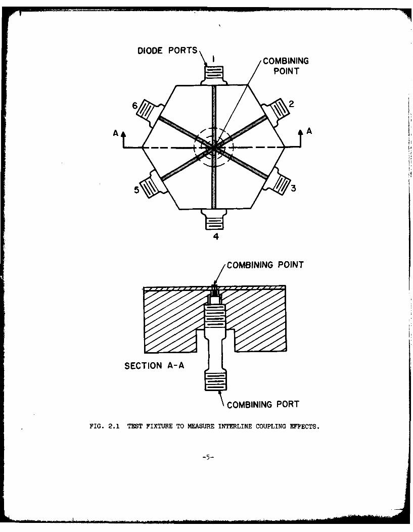
DIODE PORTSCOMBINING
POINT
A A
4
COMBINING POINT
SECTION A-A
COMBINING PORT
FIG. 2.1 TEST FIXTURE TO MEASURE INTERLINE COUPLING EFFECTS.
-5-

adjacent lines can be made by examining the transmission coefficient at
these frequencies. Figure 2.2 illustrates the transmission coefficient
S 4 and S21 over the band of frequencies, 3.5 GHz to 8.5 GHz. Virtual
short circuits appear at the combining point at approximately 4 GHz and
8 GHz. At these "virtual short" frequencies, a minimum of 22 dB of
isolation is present between adjacent lines. More isolation is present
between nonadjacent lines. At these levels of interline coupling, no
problems are expected with stability.
The experimental work in the future will concentrate on Stage
2, i.e., the characterization of diodes to be used in the combiner
circuitry. Some high-power IMPATT diodes have been obtained and will
be evaluated for their suitability and to establish combining line
lengths and characteristic impedances. Once device characterization is
complete, the diodes will be placed in the combiner circuit and the
combiner performance will be evaluated.
-6-

cc 0
zwU.
w 20 -12-
z0 16-
-20-
z< -24-
- 28-
3.5 4.5 5.5 6.5 7.5 8.5
FREQUENCY, GHz
FIG. 2.2 TRANSMISSION COEFFICIENTS VS. FREQUENCY FOR THE
POWER COMBINING CIRCUIT.
j-7

SECTION III
FET MODELING
3.1 Introduction. The objective of this phase of the program
was to develop approximate, yet realistic, models which can be employed
to predict the properties of FET devices (particularly GaAs MESFETs)
as a function of various parameters including geometry, doping profile
and operating point. Such a model has been developed and can be used,
without needing an exorbitant amount of computer time, to predict the
properties of such devices and to study the effects of the various
parameters.
A detailed technical report describing the model and the results
obtained to date has been prepared and issued as Report No. AFWAL-TR-81-
1191 entitled "GaAs FET Modeling" by J. R. East and G. I. Haddad.
3.2 The FET Model. A computer model which can be employed to
determine the operation of Schottky-barrier field-effect transistors
has been developed and is used to study a variety of transistor structures.
A summary of the major elements of the model and the results obtained to
date are summarized here.
1. A quasi-two-dimensional computer model has been developed and
the results obtained from it have been compared with other full, two-
dimensional simulations. Excellent agreement has been obtained, yet this
model is much simpler, easier to utilize and less costly to employ.
2. The effect of various depletion-layer approximations has been studied.
Although the usual depletion-layer approximation gives reasonable agreement
with other two-dimensional results, a new sloping potential methods models charge
and potential distribution within the channel better and yields better agreement.
-8-

3. A very simple model which neglects space charge in the
channel can be used to describe the FET terminal characteristics.
4. Simulations of silicon and GaAs FETs have been compared with
full, two-dimensional results. The best match between the two types of
model was for X-band GaAs FETs. Drain current vs. drain-source voltage
curves matched to approximately 15 percent. The simple quasi-two-
dimensional model predicts currents higher than the two-dimensional
models. The predictions for charge and potential distribution are also
approximately correct.
5. The effects of varying the low field mobility and saturated
velocity on the drain current vs. drain-source voltage have been studied.
Devices with mobilities and saturated velocities t 20 percent of the
nominal values were studied. The resulting drain current charge was
always less than t 20 percent, ranging from 7 to 15 percent. The effect
of the electron velocity-field curve on the current can be roughly
described by the space-charge-free model.
6. Other potential device materials have been modeled to predict
FET operation.
From these results, the properties of dc FET operation can be
described. The next step is to model RF operation of FETs. The steps
in this process are:
1. Study the small-signal operation of FETs. This involves a
small-signal expansion of the dc results. The equations for this model
have been derived and must be progranmed into the dc program.
2. Study the effect of velocity overshoot on FET operation.
3. Study the large-signal operation for a variety of conditions. This
will include frequency and power limitations under large-signal operation.
N 9OW

SECTION IV
FET CIRCUITS
4.i Introduction. The objectives of this phase of the program
were to investigate the use of FETs in a variety of useful microwave
and millimeter-wave applications. This portion of the program has been
active during the past year and work has primarily concentrated on the
large-signal characterization of FETs for use in VCOs.
A two-signal measurement technique is being implemented in conjunc-
tion with the calculator-controlled network analyzer to determine the large-
signal, two-port network properties of FETs. The data provided by this
method can be used to determine circuit conditions for the device such
that optimum oscillator performance is achieved in the form of maximum
output power, widest tuning bandwidth, or other criteria. This approach
is also useful iniue design of amplifiers using three-terminal devices
and is also useful for checking the accuracy of device models. The
characterization of devices using this method is presently underway,
and the basic measurement hardware and software requirements have been
developed.
Based on the results of the power combining study and the use of
simple FET VCO circuits, a new technique has been conceived to extend
the operating frequencies of transistor VCOs. This method uses three-
fold (or generally n-fold) symmetry to accomplish power combining
frequency tripling (n-fold multiplication) and provide a separate,
isolated output port. A patent application has been filed for this
technique and is included in Section 4.2. In addition, the Abstract
of New Technology (ANT) is included.
-10-

To summarize the efforts for this portion of the program, new
measurement techniques are being used to improve the characterization
of FETs for design and modeling purposes and the use of FETs in
frequency tripling circuits are being investigated. Enhanced perfor-
mance of this and other FET components will be possible from the
extensive experimental characterizations being performed on the
devices.
4.2 Symmetrical Frequency Tripling of Microwave Varactor
Tuned Voltage-Controlled Oscillators. The object of this invention is
to triple the output frequency of certain existing fundamental frequency
microwave varactor-tuned oscillators while providing comparable perfor-
mance with respect to tuning bandwidths, voltage-to-frequency tuning
linearity and oscillator noise levels. Additionally, the invented
technique uses symmetry to reduce the circuit design complexity and
filtering requirements over conventional methods.
The conventional approach for achieving a threefold increase
(tripling) in oscillator frequency is to use a fundamental voltage-
controlled oscillator cascaded with a separate varactor-diode or
step-recovery-diode times-three frequency multiplier (tripler)
circuit. The disadvantages of this approach are those primarily associated
with the design and realization of the frequency-tripler circuit.
Conventional frequency multiplier design requires selective filtering
requirements and specified circuit boundary conditions at the various
harmonics involved which are difficult to realize, particularly over
a wide bandwidth. Therefore, the conventional approach usually results
in narrowband operation of the voltage-controlled oscillator in
-11-

addition to low output power caused by the losses and efficiency
associated with frequency multiplication.
In the invention, fundamental-frequency voltage-controlled
oscillation and frequency tripling are accomplished in the same circuit,
and threefold symmetry is used to separate the various frequencies such
that no filtering is required to provide the frequency-tripled output
at a separate port. The construction of the invention using bipolar
junction transistors is shown in Fig. 4.1. It makes use of three
identical fundamental common-collector transistor oscillator circuits
of the type shown in Fig. 4.2 connected in a wye configuration. Each
of the three transistor oscillators in Fig. 4.1 is designed for funda-
mental frequency operation assuming points A and B are virtual short
circuits. The element values Lt, C0 , and the varactor capacitance Cv
are adjusted for a desired frequency range of oscillation. Because of
symmetry each oscillator then operates with the same electrical wave-
forms displaced in time by a third of the fundamental period or 120
electrical degrees. Hence, the three fundamental frequency currents
at nodes A and B add to zero to produce the required virtual short
circuits. The nonlinearities associated with the varactor and the
transistor will provide frequency multiplication and produce higher
harmonic currents. The second-harmonic currents will differ in phase
by twice that of the fundamental currents, resulting in these three
currents again being 120 degrees out of phase with each other and
adding to zero at the nodes A and B. Hence, A and B appear as virtual
short circuits at the second harmonic. Third-harmonic currents will
differ in phase by three times that of the fundamental currents and
hence will all be in phase at the nodes A and B. Therefore, only
-12-

Co
Co B-HT
THIRD - C0HARMONICLOAD L t
TUNING
DEVICE
FI.~ASMETIATRE-HSTIDHARMONICL
POERCOUNING, AATRTNDTASSO
OSCILLATOR.
-13-
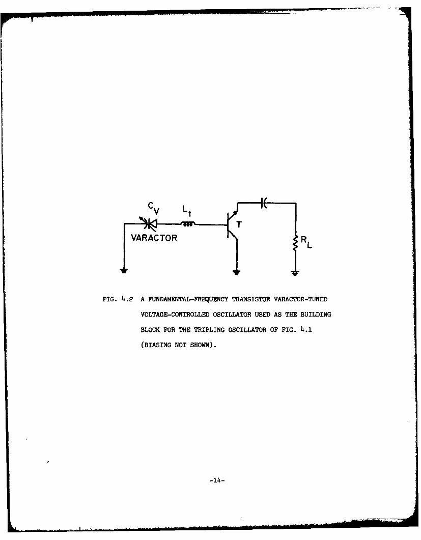
c v LI
VARACTOR RL
FIG. 4.2 A FUNDAMENTAL-FREQUENCY TRANSISTOR VARACTOR-TUNED
VOLTAGE-CONTROLLED OSCILLATOR USED AS THE BUILDING
BLOCK FOR THE TRIPLING OSCILLATOR OF FIG. 4.1
(BIASING NOT SHOWN).
-14-

third-harmonic output power will appear at these two nodes because of
the symmetry. Phasor diagrams of the currents at the fundamental,
second harmonic, and third harmonic at the node A and B are shown in
Fig. 4.3.
There are several advantages of this multiplying oscillator
circuit over the conventional approach. First, harmonic filtering is
obtained by the use of symmetry, so that wideband operation is possible
as long as the symmetry and balance of the three circuits can be
preserved. Second, the varactor accomplishes the dual role of con-
trolling the oscillator frequency and contributing to harmonic genera-
tion. It is well known that varactor diodes can produce efficient
harmonic generation in the proper circuit environment. Third, the
idling current at the second harmonic can be controlled by the nature
of the varactor and its polarity with respect to the active device.
For example, if each varactor is replaced by a back-to-back varactor
pair, the second-harmonic current can be reduced if desired. The
second-harmonic idling current can have a substantial effect on the
third-harmonic output level. Fourth, there are two points of
symmetry (A and B in Fig. 4.1) in the circuit where the third-harmonic
output power can be extracted. This allows either node to be used as
an output port with the other serving as a third-harmonic tuning loca-
tion for enhanced performance. Normally, the highest harmonic content
is expected at node A in Fig. 4.1. Last, the circuit is also combin-
ing the power output from three devices, so that higher output power
levels can be expected over the conventional approach.
This method of achieving voltage-controlled oscillation is not
constrained to use microwave bipolar transistors as indicated in Fig.
-15-

\ /
/ ///
(a) (b)
(c)
FIG. 4.3 PHASOR DIAGRAMS OF THE CURRENTS ENTERING MODE A OR B
OF FIG. 4.1 (a) AT FUNDAMENTAL FREQUENCY, (b) AT
SECOND HARMONIC AND (c) AT THIRD HARMONIC.
-16-

4.1. Other transistors, such as microwave field-effect transistors
can also be used inihe common drain configuration, for example. In
addition, two-terminal devices such as Gunn or IMPATT diodes can be
used in place of the transistors, in which case only one third-harmonic
output port will be available. Finally, when transistors are used, the
wye connection of capacitors C on the third terminals can be replaced
by an equivalent delta connection at the sacrifice of the second
third-harmonic output port. This connection may be more easily real-
ized in a planar circuit geometry.
The feature believed to be new in this invention is primarily
the use of threefold symmetry of simple fundamental oscillators to
provide one or two points of symmetry where the fundamental and
second harmonic cancel and where the third harmonic is available.
This feature is significant in that it simplifies design and elim-
inates the need for frequency selective harmonic filtering require-
ments while allowing great design flexibility at the two isolated
third-harmonic nodes. Furthermore, the circuit automatically combines
the power from three devices for improved power level at the output
while extending the effective range of operating frequencies of
fundamental-frequency microwave transistor oscillators by a factor
of three.
-17-

SECTION V
IMPATT DIODE PROPERTIES
5.1 Introduction. The purpose of this phase of the program was
to investigate in detail the various properties of IMPATT devices for
both steady-state and pulsed operation as oscillators and amplifiers.
Detailed results have been obtained for various types of profiles
including single- and double-drift devices and for various operating
points. The detailed results are included in two technical reports.
The first, which is concerned with the steady-state properties has been
issued as Report No. AFWAL-TR-81-1066 entitled "Properties of High
Efficiency X-Band GaAs IMPATT Diodes" by R. Mains and G. I. Haddad.
The second is Report No. AFWAL-TR-81-1177 entitled "Simulation of Pulsed
IMPATT Oscillators and Injection-Locked Amplifiers" by R. Mains,
G.Haddad and D. Peterson. A summary of the work performed is given in
the next section.
5.2 IMPATT Devices. The research carried out on theoretical
IMPATT investigations may be divided into two main categories. The
first was to simulate numerous single- and double-drift GaAs struc-
tures at X-band as well as to investigate operation at higher fre-
quencies and to look at some Si IMPATT structures. Second, a program
was developed to study the dynamic behavior of pulsed IMPATT oscillators
and amplifiers which utilize this simulation data. The work performed
in each of these areas is described next.
-18-

To simulate IMPATT structures, the finite difference programs
developed by Bauhahn1 were used. These programs were modified so that
total current boundary conditions are imposed for the minority carriers
(corresponding to a constant reverse saturatiun current). The dc,
small-signal and large-signal programs were all modified in this manner.
Next, an exhaustive series of runs was carried out for many GaAs IMPATT
structures designed for X-band operation which yielded information con-
cerning impedance and power levels as a function of RF voltage, dc
current density and temperature. Several structures which yield high
efficiencies due to the precollection mode were given special attention.
The single-drift structures studied were: uniformly doped, high-low,
and low-high-low doping profiles. Double-drift devices studied were:
uniformly doped, hybrid, and double Read profiles. For some of these
simulations, dynamic temperature effects were included to determine
device characteristics when the restrictive assumption that the
temperature remains constant as the RF voltage is varied is relaxed.
In addition, simulations for GaAs and Si double-drift structures
were performed in the 35- to 40-GHz range. The intent here was to
explain the high efficiencies reported in the literature 2 for GaAs
and to assess the performance of Si devices for comparison. It was
found that by suitable adjustment of the high-field diffusion coefficient
in GaAs, experimentally obtained efficiencies were duplicated.
1. Bauhahn, P. E., "Properties of Semiconductor Materials and MicrowaveTransit-Time Devices," Tech. Report No. 140, Electron Physics Lab-oratory, The University of Michigan, Ann Arbor, October 1977.
2. Masse, D., Chu, G., Johnson, K. and Adlerstein, M., "High PowerGaAs Millimeter Wave IMPATT Diodes," Microwave J., vol. 22,No. 6, pp. 103-105, June 1979.
-19-

During the second phase of the research, a program was developed
to study the dynamic oehavior of IMPATT oscillators and amplifiers
utilizing the quasi-static approximation. This approximation assumes
that the RF voltage across the device at any time may be expressed as
a sine wave whose amplitude and phase vary slowly with respect to the
RF period. Solving for the complex frequency S at each time step deter-
mines the rate of change of amplitude and phase. Temperature variation
effects are included and a thermal time constant consistent with
published values at X-band is used. The circuit is currently chosen to
model the cylindrical resonant cavity structure. The circuit model
includes package parasitics, a transmission line to model the quarter-
wave transformer near the diode, a second transmission line to model
the 50-9 line between the transformer and the resonant cavity, and a
parallel resonant lumped-element circuit to model the cavity in series
with the 50-Q stabilizing load.
This quasi-static program is being used to inexpensively investi-
gate many aspects of pulsed operation including: the delayed start
effect and how it is affected by circuit design and locking signal
amplitude, frequency drift of pulsed oscillator/amplifier during
operation, how to design for dual mode operation, the effects of varying
dc current and pulse width,and a comparison of the operating charac-
teristics of different IMPATT diode structures.
-20-

SECTION VI
MILLIMETER-WAVE IMPATT DEVICES
6.1 introduction. This phase of the program was concerned with
computer modeling of millimeter-wave IMPATT diodes. Since the applica-
bility of the conventional drift and diffusion, or static, transport
model to millimeter-wave devices is uncertain, a more general model is
needed. The new model should be of a form which allows economical
large-signal simulation of IMPATT devices. Work under this phase of
the program falls into the categories of simulation development and
application. Objectives of the development work are to develop a
suitable device model and corresponding computer program. Objectives
of the simulation work are to confirm the agreement between the con-
ventional and the new models at sufficiently low frequencies, to learn
under what circumstances the conventional model breaks down, and to
develop design guidelines for millimeter-wave IMPATT diodes.
6.2 Work Performed to Date. A transport model which conserves
carrier energy and momentum has been chosen as approiate for the
present work. The model is based on transport equations, given by
Blotekjaer,3 which are the first three velocity moments of the Boltz-
mann transport equation. A computer program which applies the model
to Si devices is now in operation. While the cost of running the
program is generally from three to ten times as large as that of
3. Blotekjaer, K., "Transport Equations for Electrons in Two-ValleySemiconductors," IEEE Trans. on Electron Devices, vol. ED-l7,No. 1, pp. 38-47, January 1970.
-21-

running a conventional simulation, numerical methods are under
investigation which may reduce the cost.
A study comparing the results of a conventional simulation
developed at the Electron Physics Laboratory4 with those of the new
simulation is underway. The two models give similar results when
applied to a Si device operating near 100 GHz, as can be seen from
the large-signal admittance data given in Fig. 6.1. The results
appear to confirm that the models are in close agreement with each
other for frequencies below 100 GHz. Some results at near 300 GHz have
also been obtained. Disagreement between the two models is great,
but may be due in part to differences between the diffusion coefficient
which is implicit in the new model and that which is used in the conven-
tional model. The coefficient used in the conventional model will be
adjusted to minimize these differences. It was thought that disagree-
ment between the two models might also be due to the use of differing
boundary conditions, but changing the conditions used in the new model
do not affect its results significantly.
6.3 Summary and Conclusions. A millimeter-wave Si IMPATT
simulation has been developed which is based on an improved transport
model. As expected, results from the new model are close to those of
the conventional drift diffusion model at sufficiently low frequencies.
The new model should provide a means of determining where the conven-
tional model breaks down and of predicting the performance of
millimeter-wave devices at very high frequencies.
4. Bauhahn, P. and Haddad, G. I., "IMPATT Device Simulation and Pro-perties," IEEE Trans. on Electron Devices, vol. ED-24, No. 6,pp. 634-64.2, June 1977.
-22-

f=130 GHz exi0
135120 ,N
E-6110 120 0
E0110 L
100 -4 zb
100 w
90 -2 un
80 85I I I-3 -2 -IxlO 3 0
CONDUCTANCE, mho/cm2
FIG. 6.1 RF ADMITTANCE AT VARIOUS FREQUErCIES PREDICTED BY
(a) ENERGY AND MOMENTUM CONSERVING SIMULATION AND
(b) CONVENTIONAL SIMULATION. (SILICON DOUBLE-DRIFT
DIODE, Jdc = 60,000 A/cm, AND VRF 10 V)
-23-

SECTION VII
CONTROLLED-AVALANCE TRANSIT-TIME TRIODE AMPLIFIERS
7.1 Introduction. The purpose of this phase of the program was
to evaluate the properties of controlled-av.lanche transit-time devices,
their application in amplifiers, and their comparison with conventional
BJT devices. This work was completed about a year ago and a technical
report s describing the results has been issued. The abstract from this
report and the summary and conclusions are included here for completeness.
7.2 Abstract from the Technical Report. "The purpose of this
work is to study the theoretical effects of avalanche multiplication
and collection transit time on microwave controlled avalanche transit-
time triode (CATT) devices. The objectives of this report are to obtain
a better device model, develop a complete one-dimensional large-signal
simulation computer program, calculate the large-signal performance of
Class C CATT amplifiers and make a comparison between Class C CATT and
Class C BJT amplifiers. The following studies were carried out in
order to achieve these objectives.
"A dc computer program was developed which calculates the dc
avalanche multiplication factor vs. base-collector dc bias character-
istics. The results provide an estimation of the suitability of
various semiconductor materials, optimum collector geometrical struc-
tures and doping densities.
5. Lee, S-W., "Controlled Avalanche Transit-Time Triode Amplifiers,"Tech. Report No. AFWAL-TR-80-1185, Electron Physics Laboratory,The Univeristy of Michigan, Ann Arbor, November 1980.
-24-

"Analytical models of dc and small-signal characteristics for
Read-type collector structures are given which incorporate both the
avalanche multiplication and collector transit-time mechanisms.
Contrary to previous findings, the small-signal characteristics
indicate that a large avalanche multiplication factor decreases the
RF power gain of small-signal Class A CATT amplifiers. The results
are given and discussed.
"A large-signal computer simulation was developed which consists
of three computer programs: the emitter-base computer program (EBCP),
the large-signal simulation program (LSSP), and the collector circuit
comptuer program (CCCP). The effects of high impurity doping level in
the emitter, high injection level inthe base, time-varying width of the
neutral base region, carrier-induced drift field in the base, nonzero
minority carrier concentration at the edge of the base-collector
depletion region in the base, and the feedback hole current are
incorporated in EBCP. Computer program LSSP models the semiconductor
region through a set of difference equations of the semiconductor
equations. A current-conserving boundary condition is given. The
simulation includes the velocity-electric field, diffusion-electric
field, and avalanche ionization rate-electric field characteristics
in the collector region. The computer program CCCP incorporates the
displacement current in the collector semiconductor region and the
effects of the external load impedance.
"Large-signal results of Class C CATT amplifiers are obtained
and are presented. Effects of base-collector dc bias, load, collector
structure, and operating frequency are discussed. The simulation cal-
culates amplifier output power, gain, and efficiency. It also gives
-25-

the emitter-base current and voltage waveforms; avalanche multiplication
factor; waveforms of voltage across the base-collector depletion region
and collector terminal current; and spatial distributions of electrons,
holes, and electric field at any time instant. Large-signal output
power, gain, efficiency, dynamic range, and inherent bandwidth of Class
C CATT and BJT amplifiers are compared and suggestions for further
studies are given."
7.3 Summary and Conclusions from the Technical Report. "The
purpose of this study was to investigate the effects of avalanche
multiplication and transit time in the collector region of a BJT.
Analytical equations, circuit models, and computer simulations were
used to determine dc, small-signal, and large-signal behavior of CATT
amplifiers.
"In Chapter II a dc computer program was developed which deter-
mines the dc avalanche multiplication factor vs. V characteristicsbias
for any Si or GaAs collector structure. The results provide an
estimation of device large-signal performance capability. The optimum
collector parameters, i.e., Wav, Nav, N c, obtained from the dc computer
program correspond well to the results of large-signal simulation.
Results also indicate that an n-type Si CATT amplifier is superior to
p-type Si and n-type GaAs CATT amplifiers due to its favorable MAo
vs. Vbias characteristics.
"In Chapter III analytical models of dc and small-signal charac-
teristics for CATT devices with Read-type collector structures were
given which incorporated both the avalanche multiplication and the
collector transit-time mechanisms. Contrary to previous findings, the
small-signal characteristics of Class A CATT amplifiers indicated that
-26-

a larger avalanche multiplication factor results in a smaller RF power
gain and an increase in MA- does not necessarily imply a significant0
increase in fm . Results were given and discussed. One conclusion
was the inapplicability of CATT devices as Class A amplifiers.
"In Chapter IV a large-signal computer simulation was developed
which incorporated several improvements over the large-signal simulation
previously reported, i.e., high injection level effects
region, Early effect, effect of high impurity level in the emitter,
nonzero minority carrier concentration at the edge of the base-collector
depletion region on the base side, minority carrier induced electric
field in the base region, current conserving boundary condition for
minority carriers in the collector region, and diffusion current in
the collector depletion region.
"In Chapter V large-signal results of Class C CATT amplifiers
were given. Effects of base-collector dc bias, load, operating frequency
and collector structures were examined and discussed. The simulation
calculates output power, power gain, and efficiency of the amplifier.
It also gives emitter-base current and voltage waveforms; avalanche
multiplication factor; JT and VT waveforms; and spatial distributions
of electrons, holes, and electric field in the collector depletion
region at any time instant. Various Si n-type CATT and BJT Class C
amplifiers operating at 12.75 GHz were compared in terms of output power,
power gain, efficiency, and dynamic range. Optimum collector impurity
doping level and optimum width of the collector region of bdth the
CATT and BJT amplifiers were determined and discussed.
-27-

Carrier multiplication and long collector transit time do increase
power gain, but at the expense of lower efficiency and smaller dynamic
range. Avalanche multiplication does help to increase the device
inherent bandwidth."
-28-

SECTION VIII
SUMKWY AND CONCLUSIONS
Several significant contributions were made during this program
toward a better understanding of microwave solid-state devices and their
behavior in oscillator and amplifier applications. In particular,
several devices were considered including CATT, IMPATT and GaAs FET
devices. Computer models were developed for analyzing the properties,
capabilities, and potential of these devices as well as determining
the types of circuits they require in order to optimize their per-
formance in oscillators and amplifiers under both CW and pulsed
conditions. Experimental measurements were also performed on some of
these devices to obtain comparison with the theoretical results. Due
to these investigations, we presently have the best computer programs
available anywhere for determining device properties, assessing their capa-
bilities and providing information as to the type of circuit impedances
required for operation of these devices as oscillators and amplifiers
as a function of frequency, geometry and doping density.
Novel schemes for power combining of devices at fundamental
and harmonic frequencies were conceived, analyzed and tested. These
schemes should lead to improved performance for combining the
power output from two- and three-terminal microwave devices and will
also prove useful in extending the frequency of operation of these
devices.
-29-