Embed Size (px)
Citation preview
This document is available at HTTP://WWW.FALCOM.DE/.
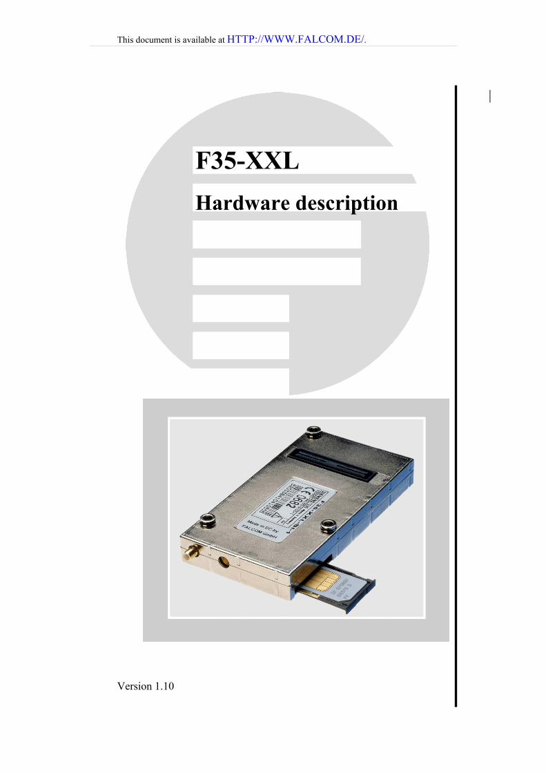
F35-XXL Hardware description
Version 1.10
F35-XXL HARDWARE DESCRIPTION VERSION 1.10
This confidential document is the property of FALCOM GmbH and may not be copied or circulated without permission. Page 1
Contents
0 INTRODUCTION ..............................................................4 0.1 GENERAL........................................................................................................................................ 4 0.2 USED ABBREVIATIONS.................................................................................................................... 6 0.3 RELATED DOCUMENTS.................................................................................................................... 8
1 SECURITY .........................................................................9 1.1 GENERAL INFORMATION................................................................................................................. 9 1.2 EXPOSURE TO RF ENERGY.............................................................................................................. 9 1.3 EFFICIENT MODEM OPERATION ....................................................................................................... 9 1.4 ANTENNA CARE AND REPLACEMENT ............................................................................................ 10 1.5 DRIVING ....................................................................................................................................... 10 1.6 ELECTRONIC DEVICES................................................................................................................... 10 1.7 VEHICLE ELECTRONIC EQUIPMENT ............................................................................................... 10 1.8 MEDICAL ELECTRONIC EQUIPMENT .............................................................................................. 10 1.9 AIRCRAFT..................................................................................................................................... 10 1.10 CHILDREN .................................................................................................................................... 11 1.11 BLASTING AREAS.......................................................................................................................... 11 1.12 POTENTIALLY EXPLOSIVE ATMOSPHERES ..................................................................................... 11 1.13 NON-IONISING RADIATION............................................................................................................ 11
2 SAFETY STANDARDS...................................................12
3 TECHNICAL DATA........................................................13
4 PIN ASSIGNMENT AND SIGNAL LEVELS...............15
5 GSM CORE ......................................................................25 5.1 TECHNICAL DATA ......................................................................................................................... 25 5.1.1 General......................................................................................................................................... 25 5.1.2 Features........................................................................................................................................ 25 5.2 HARDWARE INTERFACE................................................................................................................ 27 5.2.1 Interface for external 3 V SIM card reader .................................................................................. 27 5.2.2 Audio interface ............................................................................................................................ 28 5.2.3 Serial interface............................................................................................................................. 28 5.2.4 Control signals ............................................................................................................................. 29 5.2.4.1 Ring- MC39i................................................................................................................................................. 29 5.2.4.2 SYNC to control a status LED...................................................................................................................... 31 5.2.5 General propose input/output....................................................................................................... 32 5.2.6 General pin configuration ............................................................................................................ 32
6 GPS CORE........................................................................34 6.1 TECHNICAL DATA ......................................................................................................................... 34 6.2 TECHNICAL DESCRIPTION............................................................................................................. 36 6.2.1 Receiver Architecture .................................................................................................................. 36 6.2.2 Technical specification ................................................................................................................ 37 6.3 HARDWARE INTERFACE................................................................................................................ 38 6.3.1 Configuration and timing signals................................................................................................. 38 6.3.2 Serial communication signals ...................................................................................................... 38 6.3.3 DC input signals .......................................................................................................................... 40 6.3.4 General purpose input/output (pin 81, 110, 112, 114 and 116) ................................................... 40 6.4 SOFTWARE INTERFACE ................................................................................................................. 40 6.4.1 SiRF binary data message............................................................................................................ 41 6.4.2 NMEA data message ................................................................................................................... 43 6.4.2.1 NMEA output messages................................................................................................................................ 43 6.4.2.2 NMEA input messages.................................................................................................................................. 44
F35-XXL HARDWARE DESCRIPTION VERSION 1.10
This confidential document is the property of FALCOM GmbH and may not be copied or circulated without permission. Page 2
7 PROCESSOR CORE .......................................................46 7.1 HOW TO USE THE TCP/IP AND PPP STACK................................................................................... 50
8 GETTING STARTED......................................................51 8.1 DETERMINING THE EXTERNAL EQUIPMENT TYPE......................................................................... 51 8.2 MINIMUM HARDWARE INTERFACE TO GET STARTED..................................................................... 52
9 HOUSING .........................................................................53
10 EMC AND ESD REQUIREMENT.................................55
11 CE CONFORMITY .........................................................56
12 EVALUATION BOARD FOR F35-XXL .......................57
13 EVALUATION KIT (EVAL-KIT) .................................64
14 APPENDIX .......................................................................65 14.1 HOW TO PUT THE F35-XXL(SI) INTO THE SLEEP MODE?............................................................. 65 14.2 HOW TO COMMUNICATE WITH EXTRA EXTERNAL I2C DEVICES? .................................................. 65 14.3 HOW TO UPDATE PROGRAMMATICALLY YOUR SOFTWARE INTO THE FLASH? ............................. 65 14.4 HOW ARE THE PINS OF 120-PIN CONNECTOR CONNECTED TO THE NEC V850?............................. 65 14.5 EVAL-BOARD CIRCUIT DIAGRAM............................................................................................. 68 14.6 EVAL-BOARD PIN OUT.............................................................................................................. 70
F35-XXL HARDWARE DESCRIPTION VERSION 1.10
This confidential document is the property of FALCOM GmbH and may not be copied or circulated without permission. Page 3
Version history:
Version number Author Changes
1.00 Gerald Buch Initial version
1.01 Fadil Beqiri General, User abbreviation, Technical data, Housing, Evaluation Board for F35-XXL, Evaluation Kit (EVAL-KIT), Circuit diagram, Pin out.
1.02 Fadil Beqiri − GPS-receiver (power consumption and DC power) (G. Voigt)
− RAM-chip changed to SRAM-chip (G. Voigt) − Figure 11 (default settings for trickle power
mode) (G. Voigt) − Type of 120-pin connector (B. Kirchner)
1.03 Fadil Beqiri − In chapter 3, pin 46 (V_ANT) will be available for Power Supply to external GPS antenna (B. Kirchner).
1.04 Fadil Beqiri − Counterpart of the 120-pin connector changed.
1.05 Fadil Beqiri − The current F35-XXL(-SI) module are supplied with MC39i GSM/GPRS module instead of MC35 module.
− Pin 98 and pin 100 (GPS part) updated. − Some source code example are added − Eval-Board circuit diagram updated.
1.06 Fadil Beqiri − Misprints corrected.
1.07 Fadil Beqiri − The description of pin 63 (PWR_GOOD) on the chapter 5.2.6 updated.
− In chapter 3, external V_ANT pin is a hardware option only.
1.08 Fadil Beqiri − In chapter 6.3.2 the corresponding pin number of RxDA, RxDB and TxDA, TxDB on the board to board connector updated.
1.09 Fadil Beqiri − The Pin 108 (TMARK) changed to GPOX7 (UART RSTD)
1.10 Fadil Beqiri − The GSM/GPRS core MC35i replaced by the MC39i GSM/GPRS engine. For detailed information refer to the related documents [1.] and [2.] available on the FALCOM’s website.
F35-XXL HARDWARE DESCRIPTION VERSION 1.10
This confidential document is the property of FALCOM GmbH and may not be copied or circulated without permission. Page 4
0 Introduction
0.1 General
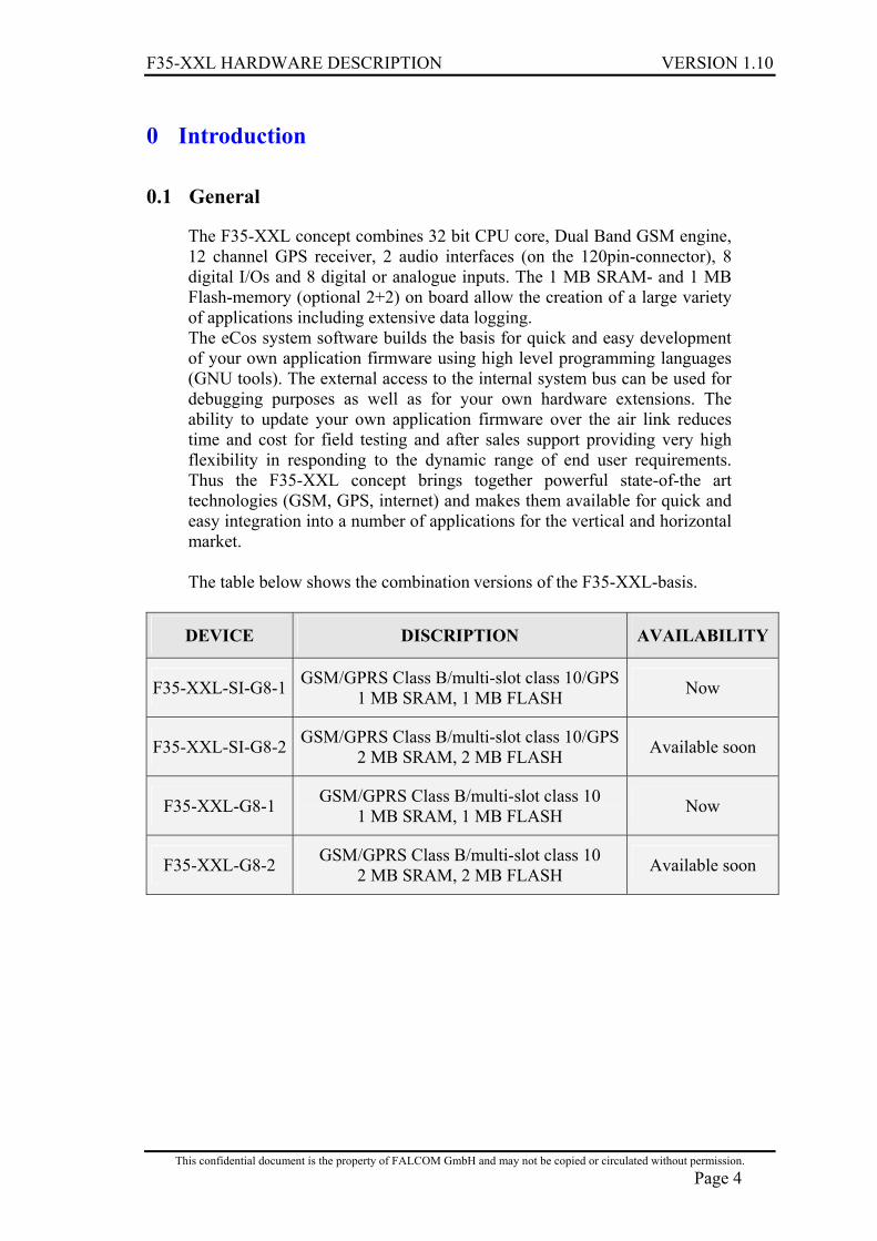
The F35-XXL concept combines 32 bit CPU core, Dual Band GSM engine, 12 channel GPS receiver, 2 audio interfaces (on the 120pin-connector), 8 digital I/Os and 8 digital or analogue inputs. The 1 MB SRAM- and 1 MB Flash-memory (optional 2+2) on board allow the creation of a large variety of applications including extensive data logging. The eCos system software builds the basis for quick and easy development of your own application firmware using high level programming languages (GNU tools). The external access to the internal system bus can be used for debugging purposes as well as for your own hardware extensions. The ability to update your own application firmware over the air link reduces time and cost for field testing and after sales support providing very high flexibility in responding to the dynamic range of end user requirements. Thus the F35-XXL concept brings together powerful state-of-the art technologies (GSM, GPS, internet) and makes them available for quick and easy integration into a number of applications for the vertical and horizontal market. The table below shows the combination versions of the F35-XXL-basis.
DEVICE DISCRIPTION AVAILABILITY
F35-XXL-SI-G8-1 GSM/GPRS Class B/multi-slot class 10/GPS 1 MB SRAM, 1 MB FLASH Now
F35-XXL-SI-G8-2 GSM/GPRS Class B/multi-slot class 10/GPS2 MB SRAM, 2 MB FLASH Available soon
F35-XXL-G8-1 GSM/GPRS Class B/multi-slot class 10 1 MB SRAM, 1 MB FLASH Now
F35-XXL-G8-2 GSM/GPRS Class B/multi-slot class 10 2 MB SRAM, 2 MB FLASH Available soon
F35-XXL HARDWARE DESCRIPTION VERSION 1.10
This confidential document is the property of FALCOM GmbH and may not be copied or circulated without permission. Page 5
Figure 1: Architecture of the F35-XXL-SI
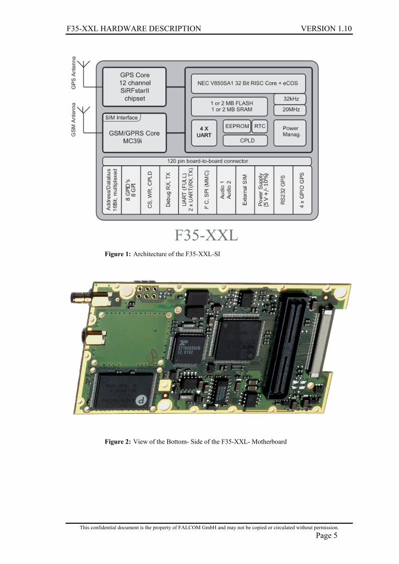
Figure 2: View of the Bottom- Side of the F35-XXL- Motherboard
F35-XXL HARDWARE DESCRIPTION VERSION 1.10
This confidential document is the property of FALCOM GmbH and may not be copied or circulated without permission. Page 6
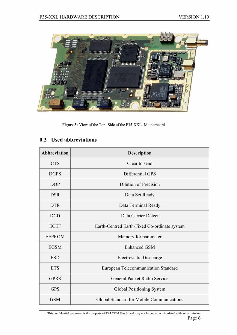
Figure 3: View of the Top- Side of the F35-XXL- Motherboard
0.2 Used abbreviations
Abbreviation Description
CTS Clear to send
DGPS Differential GPS
DOP Dilution of Precision
DSR Data Set Ready
DTR Data Terminal Ready
DCD Data Carrier Detect
ECEF Earth-Centred Earth-Fixed Co-ordinate system
EEPROM Memory for parameter
EGSM Enhanced GSM
ESD Electrostatic Discharge
ETS European Telecommunication Standard
GPRS General Packet Radio Service
GPS Global Positioning System
GSM Global Standard for Mobile Communications
F35-XXL HARDWARE DESCRIPTION VERSION 1.10
This confidential document is the property of FALCOM GmbH and may not be copied or circulated without permission. Page 7
Abbreviation Description
GGA GPS Fixed Data
HDOP Horizontal DOP
HW Hardware
IMEI International Mobile Equipment Identity
I/O Input/Output
NMEA National Maritime Electronics Association
PRN Pseudorandom Noise Number – The Identity of GPS satellites
RF Radio Frequency
RI Ring Indication
RP Receive Protocol
RTC Real Time Clock
RTCM Radio Technical Commission for Maritime Services
RTS Ready To Send
Rx Receive direction
RXD Data input
RXQUAL Received Signal Quality
SIM Subscriber Identification Module
SMS Short Message Service
SRAM Static Random Access Memory
SW Software
TA Terminal Adapter
TE Terminal Equipment
TP Transmit Protocol
TTFF Time to First Fix
Tx Transmit direction
F35-XXL HARDWARE DESCRIPTION VERSION 1.10
This confidential document is the property of FALCOM GmbH and may not be copied or circulated without permission. Page 8
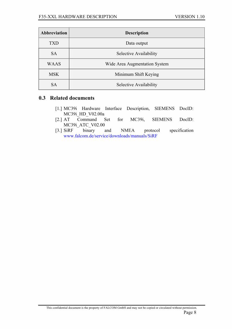
Abbreviation Description
TXD Data output
SA Selective Availability
WAAS Wide Area Augmentation System
MSK Minimum Shift Keying
SA Selective Availability
0.3 Related documents
[1.] MC39i Hardware Interface Description, SIEMENS DocID: MC39i_HD_V02.00a
[2.] AT Command Set for MC39i, SIEMENS DocID: MC39i_ATC_V02.00
[3.] SiRF binary and NMEA protocol specification www.falcom.de/service/downloads/manuals/SiRF
F35-XXL HARDWARE DESCRIPTION VERSION 1.10
This confidential document is the property of FALCOM GmbH and may not be copied or circulated without permission. Page 9
1 Security
IMPORTANT FOR THE EFFICIENT AND SAFE OPERATION OF YOUR GSM-MODEM, READ THIS INFORMATION BEFORE USE!
Your cellular engine F35-XXL is one of the most exciting and innovative electronic products ever developed. With it you can stay in contact with your office, your home, emergency services and others, wherever service is provided. This chapter contains important information for the safe and reliable use of the F35-XXL. Please read this chapter carefully before starting to use the cellular engine F35-XXL.
1.1 General information
Your F35-XXL utilises the GSM standard for cellular technology. GSM is a newer radio frequency („RF“) technology than the current FM technology that has been used for radio communications for decades. The GSM standard has been established for use in the European community and elsewhere. Your modem is actually a low power radio transmitter and receiver. It sends out and receives radio frequency energy. When you use your modem, the cellular system handling your calls controls both the radio frequency and the power level of your cellular modem.
1.2 Exposure to RF energy
There has been some public concern about possible health effects of using GSM modem. Although research on health effects from RF energy has focused for many years on the current RF technology, scientists have begun research regarding newer radio technologies, such as GSM. After existing research had been reviewed, and after compliance to all applicable safety standards had been tested, it has been concluded that the product is fit for use. If you are concerned about exposure to RF energy there are things you can do to minimise exposure. Obviously, limiting the duration of your calls will reduce your exposure to RF energy. In addition, you can reduce RF exposure by operating your cellular modem efficiently by following the guidelines below.
1.3 Efficient modem operation
In order to operate your modem at the lowest power level, consistent with satisfactory call quality please take note of the following hints. If your modem has an extendible antenna, extend it fully. Some models allow you to place a call with the antenna retracted. However your modem operates more efficiently with the antenna fully extended. Do not hold the antenna when the modem is „IN USE“. Holding the antenna affects call quality and may cause the modem to operate at a higher power level than needed.
F35-XXL HARDWARE DESCRIPTION VERSION 1.10
This confidential document is the property of FALCOM GmbH and may not be copied or circulated without permission. Page 10
1.4 Antenna care and replacement
Do not use the modem with a damaged antenna. If a damaged antenna comes into contact with the skin, a minor burn may result. Replace a damaged antenna immediately. Consult your manual to see if you may change the antenna yourself. If so, use only a manufacturer-approved antenna. Otherwise, have your antenna repaired by a qualified technician. Use only the supplied or approved antenna. Unauthorised antennas, modifications or attachments could damage the modem and may contravene local RF emission regulations or invalidate type approval.
1.5 Driving
Check the laws and regulations on the use of cellular devices in the area where you drive. Always obey them. Also, when using your modem while driving, please pay full attention to driving, pull off the road and park before making or answering a call if driving conditions so require. When applications are prepared for mobile use they should fulfil road-safety instructions of the current law!
1.6 Electronic devices
Most electronic equipment, for example in hospitals and motor vehicles is shielded from RF energy. However RF energy may affect some malfunctioning or improperly shielded electronic equipment.
1.7 Vehicle electronic equipment
Check your vehicle manufacturer's representative to determine if any on board electronic equipment is adequately shielded from RF energy.
1.8 Medical electronic equipment
Consult the manufacturer of any personal medical devices (such as pacemakers, hearing aids, etc.) to determine if they are adequately shielded from external RF energy. Turn your F35-XXL OFF in health care facilities when any regulations posted in the area instruct you to do so. Hospitals or health care facilities may be using RF monitoring equipment.
1.9 Aircraft
Turn your F35-XXL OFF before boarding any aircraft. Use it on the ground only with crew permission. Do not use it in the air. To prevent possible interference with aircraft systems, Federal Aviation Administration (FAA) regulations require you to have permission from a crew member to use your modem while the plane is on the ground. To prevent interference with cellular systems, local RF regulations prohibit using your modem whilst airborne.
F35-XXL HARDWARE DESCRIPTION VERSION 1.10
This confidential document is the property of FALCOM GmbH and may not be copied or circulated without permission. Page 11
1.10 Children
Do not allow children to play with your F35-XXL. It is not a toy. Children could hurt themselves or others (by poking themselves or others in the eye with the antenna, for example). Children could damage the modem or make calls that increase your modem bills.
1.11 Blasting areas
To avoid interfering with blasting operations, turn your unit OFF when in a "blasting area" or in areas posted: „turn off two-way radio“. Construction crew often use remote control RF devices to set off explosives.
1.12 Potentially explosive atmospheres
Turn your F35-XXL OFF when in any area with a potentially explosive atmosphere. It is rare, but your modem or its accessories could generate sparks. Sparks in such areas could cause an explosion or fire resulting in bodily injury or even death. Areas with a potentially explosive atmosphere are often, but not always, clearly marked. They include fuelling areas such as petrol stations; below decks on boats; fuel or chemical transfer or storage facilities; and areas where the air contains chemicals or particles, such as grain, dust or metal powders. Do not transport or store flammable gas, liquid or explosives, in the compartment of your vehicle which contains your modem or accessories. Before using your modem in a vehicle powered by liquefied petroleum gas (such as propane or butane) ensure that the vehicle complies with the relevant fire and safety regulations of the country in which the vehicle is to be used.
1.13 Non-ionising radiation
As with other mobile radio transmitting equipment users are advised that for satisfactory operation and for the safety of personnel, it is recommended that no part of the human body be allowed to come too close to the antenna during operation of the equipment. The radio equipment shall be connected to the antenna via a non-radiating 50 Ohm coaxial cable. The antenna shall be mounted in such a position that no part of the human body will normally rest close to any part of the antenna. It is also recommended to use the equipment not close to medical devices as for example hearing aids and pacemakers.
F35-XXL HARDWARE DESCRIPTION VERSION 1.10
This confidential document is the property of FALCOM GmbH and may not be copied or circulated without permission. Page 12
2 Safety standards
The GSM core complies with all applicable RF safety standards. The embedded GMS modem meets the safety standards for RF receivers and the standards and recommendations for the protection of public exposure to RF electromagnetic energy established by government bodies and professional organizations, such as directives of the European Community, Directorate General V in matters of radio frequency electromagnetic energy.
F35-XXL HARDWARE DESCRIPTION VERSION 1.10
This confidential document is the property of FALCOM GmbH and may not be copied or circulated without permission. Page 13
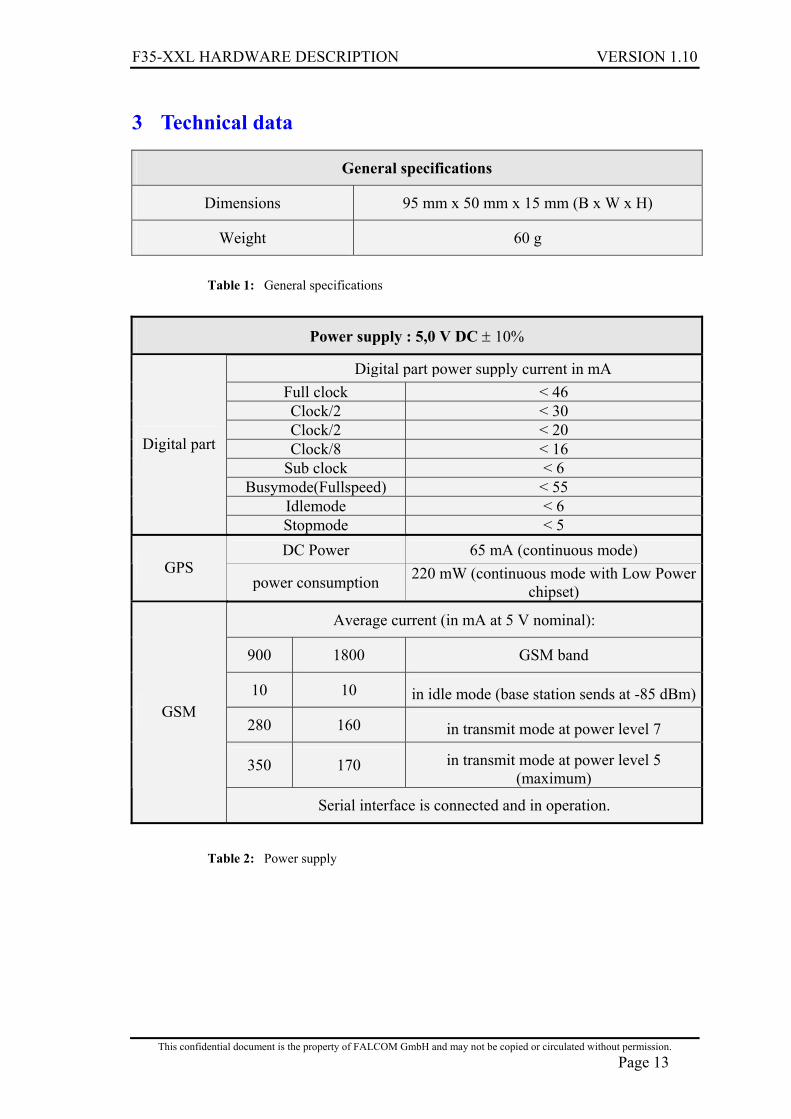
3 Technical data
General specifications
Dimensions 95 mm x 50 mm x 15 mm (B x W x H)
Weight 60 g
Table 1: General specifications
Power supply : 5,0 V DC ± 10%
Digital part power supply current in mA Full clock < 46 Clock/2 < 30 Clock/2 < 20 Clock/8 < 16
Sub clock < 6 Busymode(Fullspeed) < 55
Idlemode < 6
Digital part
Stopmode < 5 DC Power 65 mA (continuous mode)
GPS power consumption 220 mW (continuous mode with Low Power
chipset)
Average current (in mA at 5 V nominal):
900 1800 GSM band
10 10 in idle mode (base station sends at -85 dBm)
280 160 in transmit mode at power level 7
350 170 in transmit mode at power level 5 (maximum)
GSM
Serial interface is connected and in operation.
Table 2: Power supply
F35-XXL HARDWARE DESCRIPTION VERSION 1.10
This confidential document is the property of FALCOM GmbH and may not be copied or circulated without permission. Page 14
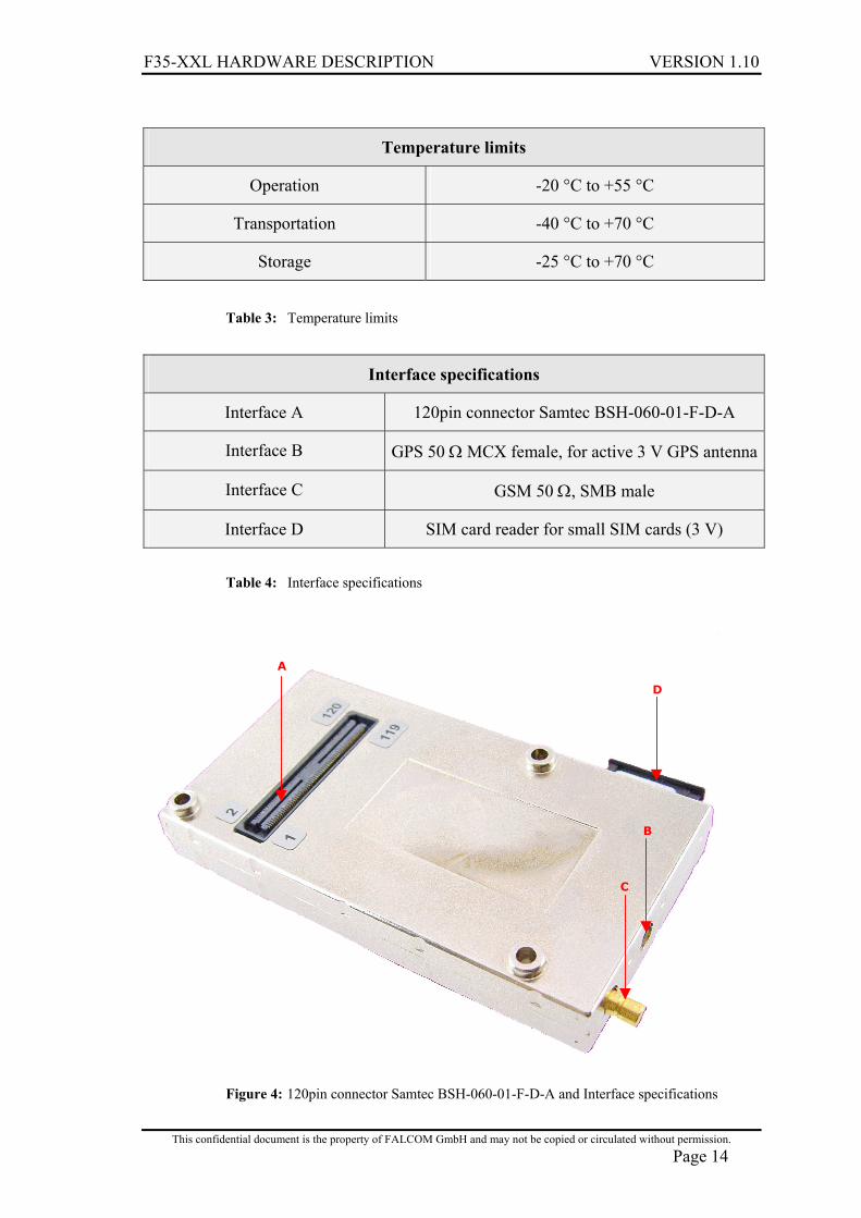
Temperature limits
Operation -20 °C to +55 °C
Transportation -40 °C to +70 °C
Storage -25 °C to +70 °C
Table 3: Temperature limits
Interface specifications
Interface A 120pin connector Samtec BSH-060-01-F-D-A
Interface B GPS 50 Ω MCX female, for active 3 V GPS antenna
Interface C GSM 50 Ω, SMB male
Interface D SIM card reader for small SIM cards (3 V)
Table 4: Interface specifications
Figure 4: 120pin connector Samtec BSH-060-01-F-D-A and Interface specifications
A
B
D
C
F35-XXL HARDWARE DESCRIPTION VERSION 1.10
This confidential document is the property of FALCOM GmbH and may not be copied or circulated without permission. Page 15
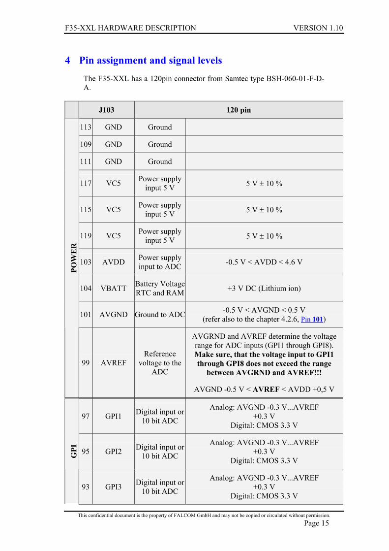
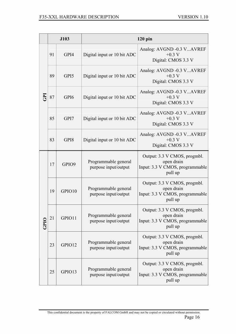
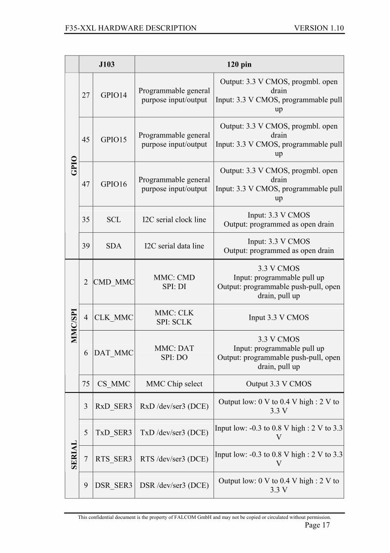
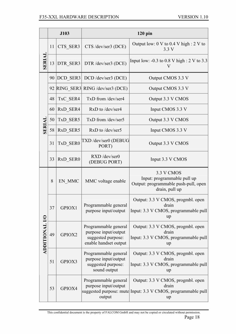
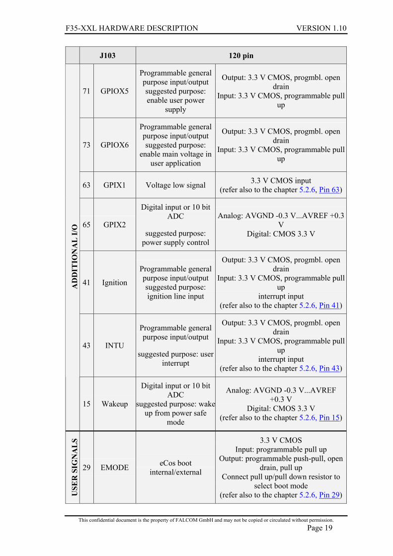
4 Pin assignment and signal levels
The F35-XXL has a 120pin connector from Samtec type BSH-060-01-F-D-A.
J103 120 pin
113 GND Ground
109 GND Ground
111 GND Ground
117 VC5 Power supply input 5 V 5 V ± 10 %
115 VC5 Power supply input 5 V 5 V ± 10 %
119 VC5 Power supply input 5 V 5 V ± 10 %
103 AVDD Power supply input to ADC -0.5 V < AVDD < 4.6 V
104 VBATT Battery Voltage RTC and RAM +3 V DC (Lithium ion)
101 AVGND Ground to ADC -0.5 V < AVGND < 0.5 V (refer also to the chapter 4.2.6, Pin 101)
POW
ER
99 AVREF Reference
voltage to the ADC
AVGRND and AVREF determine the voltage range for ADC inputs (GPI1 through GPI8). Make sure, that the voltage input to GPI1 through GPI8 does not exceed the range
between AVGRND and AVREF!!!
AVGND -0.5 V < AVREF < AVDD +0,5 V
97 GPI1 Digital input or 10 bit ADC
Analog: AVGND -0.3 V...AVREF +0.3 V
Digital: CMOS 3.3 V
95 GPI2 Digital input or 10 bit ADC
Analog: AVGND -0.3 V...AVREF +0.3 V
Digital: CMOS 3.3 V GPI
93 GPI3 Digital input or 10 bit ADC
Analog: AVGND -0.3 V...AVREF +0.3 V
Digital: CMOS 3.3 V
F35-XXL HARDWARE DESCRIPTION VERSION 1.10
This confidential document is the property of FALCOM GmbH and may not be copied or circulated without permission. Page 16
J103 120 pin
91 GPI4 Digital input or 10 bit ADCAnalog: AVGND -0.3 V...AVREF
+0.3 V Digital: CMOS 3.3 V
89 GPI5 Digital input or 10 bit ADCAnalog: AVGND -0.3 V...AVREF
+0.3 V Digital: CMOS 3.3 V
87 GPI6 Digital input or 10 bit ADCAnalog: AVGND -0.3 V...AVREF
+0.3 V Digital: CMOS 3.3 V
85 GPI7 Digital input or 10 bit ADCAnalog: AVGND -0.3 V...AVREF
+0.3 V Digital: CMOS 3.3 V
GPI
83 GPI8 Digital input or 10 bit ADCAnalog: AVGND -0.3 V...AVREF
+0.3 V Digital: CMOS 3.3 V
17 GPIO9 Programmable general purpose input/output
Output: 3.3 V CMOS, progmbl. open drain
Input: 3.3 V CMOS, programmable pull up
19 GPIO10 Programmable general purpose input/output
Output: 3.3 V CMOS, progmbl. open drain
Input: 3.3 V CMOS, programmable pull up
21 GPIO11 Programmable general purpose input/output
Output: 3.3 V CMOS, progmbl. open drain
Input: 3.3 V CMOS, programmable pull up
23 GPIO12 Programmable general purpose input/output
Output: 3.3 V CMOS, progmbl. open drain
Input: 3.3 V CMOS, programmable pull up
GPI
O
25 GPIO13 Programmable general purpose input/output
Output: 3.3 V CMOS, progmbl. open drain
Input: 3.3 V CMOS, programmable pull up
F35-XXL HARDWARE DESCRIPTION VERSION 1.10
This confidential document is the property of FALCOM GmbH and may not be copied or circulated without permission. Page 17
J103 120 pin
27 GPIO14 Programmable general purpose input/output
Output: 3.3 V CMOS, progmbl. open drain
Input: 3.3 V CMOS, programmable pull up
45 GPIO15 Programmable general purpose input/output
Output: 3.3 V CMOS, progmbl. open drain
Input: 3.3 V CMOS, programmable pull up
47 GPIO16 Programmable general purpose input/output
Output: 3.3 V CMOS, progmbl. open drain
Input: 3.3 V CMOS, programmable pull up
35 SCL I2C serial clock line Input: 3.3 V CMOS Output: programmed as open drain
GPI
O
39 SDA I2C serial data line Input: 3.3 V CMOS Output: programmed as open drain
2 CMD_MMC MMC: CMD SPI: DI
3.3 V CMOS Input: programmable pull up
Output: programmable push-pull, open drain, pull up
4 CLK_MMC MMC: CLK SPI: SCLK Input 3.3 V CMOS
6 DAT_MMC MMC: DAT SPI: DO
3.3 V CMOS Input: programmable pull up
Output: programmable push-pull, open drain, pull up
MM
C/S
PI
75 CS_MMC MMC Chip select Output 3.3 V CMOS
3 RxD_SER3 RxD /dev/ser3 (DCE) Output low: 0 V to 0.4 V high : 2 V to 3.3 V
5 TxD_SER3 TxD /dev/ser3 (DCE) Input low: -0.3 to 0.8 V high : 2 V to 3.3 V
7 RTS_SER3 RTS /dev/ser3 (DCE) Input low: -0.3 to 0.8 V high : 2 V to 3.3 V SE
RIA
L
9 DSR_SER3 DSR /dev/ser3 (DCE) Output low: 0 V to 0.4 V high : 2 V to 3.3 V
F35-XXL HARDWARE DESCRIPTION VERSION 1.10
This confidential document is the property of FALCOM GmbH and may not be copied or circulated without permission. Page 18
J103 120 pin
11 CTS_SER3 CTS /dev/ser3 (DCE) Output low: 0 V to 0.4 V high : 2 V to 3.3 V
SER
IAL
13 DTR_SER3 DTR /dev/ser3 (DCE) Input low: -0.3 to 0.8 V high : 2 V to 3.3 V
90 DCD_SER3 DCD /dev/ser3 (DCE) Output CMOS 3.3 V
92 RING_SER3 RING /dev/ser3 (DCE) Output CMOS 3.3 V
48 TxC_SER4 TxD from /dev/ser4 Output 3.3 V CMOS
60 RxD_SER4 RxD to /dev/ser4 Input CMOS 3.3 V
50 TxD_SER5 TxD from /dev/ser5 Output 3.3 V CMOS
58 RxD_SER5 RxD to /dev/ser5 Input CMOS 3.3 V
31 TxD_SER0 TXD /dev/ser0 (DEBUG PORT) Output 3.3 V CMOS
SER
IAL
33 RxD_SER0 RXD /dev/ser0 (DEBUG PORT) Input 3.3 V CMOS
8 EN_MMC MMC voltage enable
3.3 V CMOS Input: programmable pull up
Output: programmable push-pull, open drain, pull up
37 GPIOX1 Programmable general purpose input/output
Output: 3.3 V CMOS, progmbl. open drain
Input: 3.3 V CMOS, programmable pull up
49 GPIOX2
Programmable general purpose input/output suggested purpose:
enable handset output
Output: 3.3 V CMOS, progmbl. open drain
Input: 3.3 V CMOS, programmable pull up
51 GPIOX3
Programmable general purpose input/output suggested purpose:
sound output
Output: 3.3 V CMOS, progmbl. open drain
Input: 3.3 V CMOS, programmable pull up
AD
DIT
ION
AL
I/O
53 GPIOX4
Programmable general purpose input/output
suggested purpose: mute output
Output: 3.3 V CMOS, progmbl. open drain
Input: 3.3 V CMOS, programmable pull up
F35-XXL HARDWARE DESCRIPTION VERSION 1.10
This confidential document is the property of FALCOM GmbH and may not be copied or circulated without permission. Page 19
J103 120 pin
71 GPIOX5
Programmable general purpose input/output suggested purpose: enable user power
supply
Output: 3.3 V CMOS, progmbl. open drain
Input: 3.3 V CMOS, programmable pull up
73 GPIOX6
Programmable general purpose input/output suggested purpose:
enable main voltage in user application
Output: 3.3 V CMOS, progmbl. open drain
Input: 3.3 V CMOS, programmable pull up
63 GPIX1 Voltage low signal 3.3 V CMOS input (refer also to the chapter 5.2.6, Pin 63)
65 GPIX2
Digital input or 10 bit ADC
suggested purpose: power supply control
Analog: AVGND -0.3 V...AVREF +0.3 V
Digital: CMOS 3.3 V
41 Ignition
Programmable general purpose input/output suggested purpose: ignition line input
Output: 3.3 V CMOS, progmbl. open drain
Input: 3.3 V CMOS, programmable pull up
interrupt input (refer also to the chapter 5.2.6, Pin 41)
43 INTU
Programmable general purpose input/output
suggested purpose: user interrupt
Output: 3.3 V CMOS, progmbl. open drain
Input: 3.3 V CMOS, programmable pull up
interrupt input (refer also to the chapter 5.2.6, Pin 43)
AD
DIT
ION
AL
I/O
15 Wakeup
Digital input or 10 bit ADC
suggested purpose: wake up from power safe
mode
Analog: AVGND -0.3 V...AVREF +0.3 V
Digital: CMOS 3.3 V (refer also to the chapter 5.2.6, Pin 15)
USE
R S
IGN
AL
S
29 EMODE eCos boot internal/external
3.3 V CMOS Input: programmable pull up
Output: programmable push-pull, open drain, pull up
Connect pull up/pull down resistor to select boot mode
(refer also to the chapter 5.2.6, Pin 29)
F35-XXL HARDWARE DESCRIPTION VERSION 1.10
This confidential document is the property of FALCOM GmbH and may not be copied or circulated without permission. Page 20
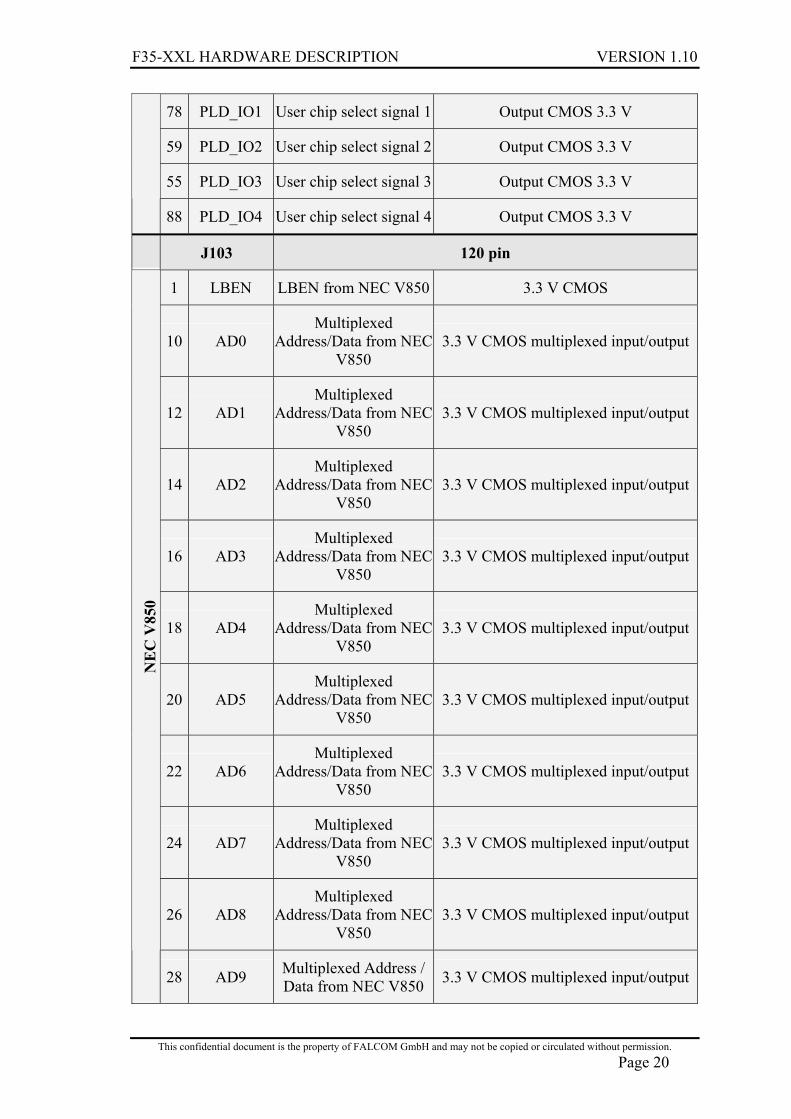
78 PLD_IO1 User chip select signal 1 Output CMOS 3.3 V
59 PLD_IO2 User chip select signal 2 Output CMOS 3.3 V
55 PLD_IO3 User chip select signal 3 Output CMOS 3.3 V
88 PLD_IO4 User chip select signal 4 Output CMOS 3.3 V
J103 120 pin
1 LBEN LBEN from NEC V850 3.3 V CMOS
10 AD0 Multiplexed
Address/Data from NEC V850
3.3 V CMOS multiplexed input/output
12 AD1 Multiplexed
Address/Data from NEC V850
3.3 V CMOS multiplexed input/output
14 AD2 Multiplexed
Address/Data from NEC V850
3.3 V CMOS multiplexed input/output
16 AD3 Multiplexed
Address/Data from NEC V850
3.3 V CMOS multiplexed input/output
18 AD4 Multiplexed
Address/Data from NEC V850
3.3 V CMOS multiplexed input/output
20 AD5 Multiplexed
Address/Data from NEC V850
3.3 V CMOS multiplexed input/output
22 AD6 Multiplexed
Address/Data from NEC V850
3.3 V CMOS multiplexed input/output
24 AD7 Multiplexed
Address/Data from NEC V850
3.3 V CMOS multiplexed input/output
26 AD8 Multiplexed
Address/Data from NEC V850
3.3 V CMOS multiplexed input/output
NE
C V
850
28 AD9 Multiplexed Address / Data from NEC V850 3.3 V CMOS multiplexed input/output
F35-XXL HARDWARE DESCRIPTION VERSION 1.10
This confidential document is the property of FALCOM GmbH and may not be copied or circulated without permission. Page 21
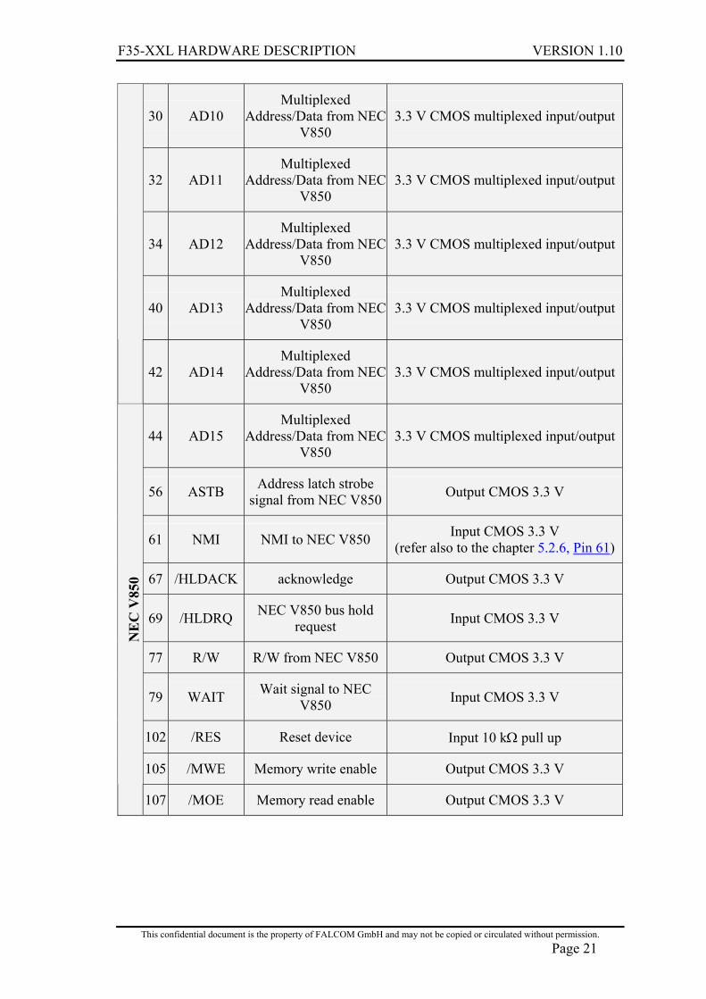
30 AD10 Multiplexed
Address/Data from NEC V850
3.3 V CMOS multiplexed input/output
32 AD11 Multiplexed
Address/Data from NEC V850
3.3 V CMOS multiplexed input/output
34 AD12 Multiplexed
Address/Data from NEC V850
3.3 V CMOS multiplexed input/output
40 AD13 Multiplexed
Address/Data from NEC V850
3.3 V CMOS multiplexed input/output
42 AD14 Multiplexed
Address/Data from NEC V850
3.3 V CMOS multiplexed input/output
44 AD15 Multiplexed
Address/Data from NEC V850
3.3 V CMOS multiplexed input/output
56 ASTB Address latch strobe signal from NEC V850 Output CMOS 3.3 V
61 NMI NMI to NEC V850 Input CMOS 3.3 V (refer also to the chapter 5.2.6, Pin 61)
67 /HLDACK acknowledge Output CMOS 3.3 V
69 /HLDRQ NEC V850 bus hold request Input CMOS 3.3 V
77 R/W R/W from NEC V850 Output CMOS 3.3 V
79 WAIT Wait signal to NEC V850 Input CMOS 3.3 V
102 /RES Reset device Input 10 kΩ pull up
105 /MWE Memory write enable Output CMOS 3.3 V
NE
C V
850
107 /MOE Memory read enable Output CMOS 3.3 V
F35-XXL HARDWARE DESCRIPTION VERSION 1.10
This confidential document is the property of FALCOM GmbH and may not be copied or circulated without permission. Page 22
J103 120 pin
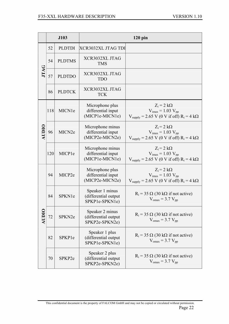
52 PLDTDI XCR3032XL JTAG TDI
54 PLDTMS XCR3032XL JTAG TMS
57 PLDTDO XCR3032XL JTAG TDO JT
AG
86 PLDTCK XCR3032XL JTAG TCK
118 MICN1e Microphone plus differential input
(MICP1e-MICN1e)
Zi = 2 kΩ Vimax = 1.03 Vpp
Vsupply = 2.65 V (0 V if off) Ri = 4 kΩ
96 MICN2e Microphone minus differential input
(MICP2e-MICN2e)
Zi = 2 kΩ Vimax = 1.03 Vpp
Vsupply = 2.65 V (0 V if off) Ri = 4 kΩ AU
DIO
120 MICP1e Microphone minus differential input
(MICP1e-MICN1e)
Zi = 2 kΩ Vimax = 1.03 Vpp
Vsupply = 2.65 V (0 V if off) Ri = 4 kΩ
94 MICP2e Microphone plus differential input
(MICP2e-MICN2e)
Zi = 2 kΩ Vimax = 1.03 Vpp
Vsupply = 2.65 V (0 V if off) Ri = 4 kΩ
84 SPKN1e Speaker 1 minus
(differential output SPKP1e-SPKN1e)
Ri = 35 Ω (30 kΩ if not active) Vomax = 3.7 Vpp
72 SPKN2e Speaker 2 minus
(differential output SPKP2e-SPKN2e)
Ri = 35 Ω (30 kΩ if not active) Vomax = 3.7 Vpp
82 SPKP1e Speaker 1 plus
(differential output SPKP1e-SPKN1e)
Ri = 35 Ω (30 kΩ if not active) Vomax = 3.7 Vpp
AU
DIO
70 SPKP2e Speaker 2 plus
(differential output SPKP2e-SPKN2e)
Ri = 35 Ω (30 kΩ if not active) Vomax = 3.7 Vpp
F35-XXL HARDWARE DESCRIPTION VERSION 1.10
This confidential document is the property of FALCOM GmbH and may not be copied or circulated without permission. Page 23
J103 120 pin
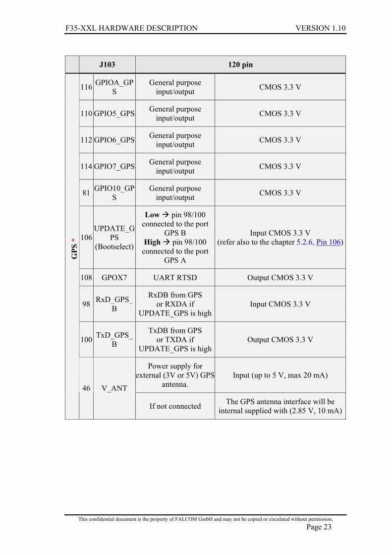
116 GPIOA_GPS
General purpose input/output CMOS 3.3 V
110 GPIO5_GPS General purpose input/output CMOS 3.3 V
112 GPIO6_GPS General purpose input/output CMOS 3.3 V
114 GPIO7_GPS General purpose input/output CMOS 3.3 V
81 GPIO10_GPS
General purpose input/output CMOS 3.3 V
106 UPDATE_G
PS (Bootselect)
Low pin 98/100 connected to the port
GPS B High pin 98/100
connected to the port GPS A
Input CMOS 3.3 V (refer also to the chapter 5.2.6, Pin 106)
108 GPOX7 UART RTSD Output CMOS 3.3 V
98 RxD_GPS_B
RxDB from GPS or RXDA if
UPDATE_GPS is highInput CMOS 3.3 V
100 TxD_GPS_B
TxDB from GPS or TXDA if
UPDATE_GPS is highOutput CMOS 3.3 V
Power supply for external (3V or 5V) GPS
antenna. Input (up to 5 V, max 20 mA)
GPS
*
46 V_ANT
If not connected The GPS antenna interface will be internal supplied with (2.85 V, 10 mA)
F35-XXL HARDWARE DESCRIPTION VERSION 1.10
This confidential document is the property of FALCOM GmbH and may not be copied or circulated without permission. Page 24
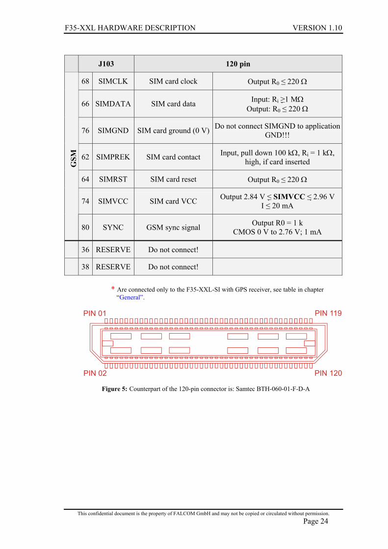
J103 120 pin
68 SIMCLK SIM card clock Output R0 ≤ 220 Ω
66 SIMDATA SIM card data Input: Ri ≥1 MΩ Output: R0 ≤ 220 Ω
76 SIMGND SIM card ground (0 V) Do not connect SIMGND to application GND!!!
62 SIMPREK SIM card contact Input, pull down 100 kΩ, Ri = 1 kΩ, high, if card inserted
64 SIMRST SIM card reset Output R0 ≤ 220 Ω
74 SIMVCC SIM card VCC Output 2.84 V ≤ SIMVCC ≤ 2.96 V I ≤ 20 mA
GSM
80 SYNC GSM sync signal Output R0 = 1 k CMOS 0 V to 2.76 V; 1 mA
36 RESERVE Do not connect!
38 RESERVE Do not connect!
* Are connected only to the F35-XXL-SI with GPS receiver, see table in chapter
“General”.
PIN 01 PIN 119
PIN 120PIN 02
Figure 5: Counterpart of the 120-pin connector is: Samtec BTH-060-01-F-D-A
F35-XXL HARDWARE DESCRIPTION VERSION 1.10
This confidential document is the property of FALCOM GmbH and may not be copied or circulated without permission. Page 25
5 GSM core
5.1 Technical data
5.1.1 General
The cellular engine F35-XXL operates in GSM 900 MHz and GSM 1800 MHz frequency bands. Designed to easily provide radio connection for voice and data transmission the F35-XXL integrate seamlessly with a wide range of GSM application platforms and are ideally suited to design and set up innovative cellular solutions with minimum effort. The F35-XXL-GPRS supports GPRS multi-slot class 10 (3 Rx, 2 Tx time slot) and GPRS coding schemes CS-1, CS-2, CS-3 and CS-4. It operates in the frequency band GSM 900 MHz and GSM 1800 MHz.
5.1.2 Features
Feature Implementation
Transmission Voice, data, SMS, fax
Power supply Single supply voltage 5 V Please refer to chapter 8 for more detailed information
Frequency bands Dual Band EGSM 900 and GSM 1800 (GSM Phase 2+)
GSM class Small MS
Transmit power Class 4 (2W) for EGSM 900 Class 1 (1W) for GSM 1800
SIM card reader External – connected via interface connector Internal SIM card reader for small 3 V SIM cards
External antenna Connected via 50 Ohm antenna connector
Speech codec
Triple rate codec: Half Rate (ETS 06.20) Full Rate (ETS 06.10)
Enhanced Full Rate(ETS 06.50 / 06.60 / 06.80)
SMS MT, MO, CB, Text and PDU mode
F35-XXL HARDWARE DESCRIPTION VERSION 1.10
This confidential document is the property of FALCOM GmbH and may not be copied or circulated without permission. Page 26
Feature Implementation
DATA
Transmission rates: 2.4, 4.8, 9.6 kbps additional 14.4 kbps, non-transparent
F35-XXL-GPRS: GPRS multi-slot class 10
GPRS mobile station class 10 GPRS: max. 85.6 kbps (down link)
USSD Coding scheme: CS 1, 2, 3, 4
PPP-stack
FAX Group 3: Class 1, Class 2
Audio interface
Analog voice: Microphone
Earpiece Hands free (supports echo cancellation and noise reduction)
Interfaces RS232 (CMOS level) bi-directional bus for commands/data usingAT commands
Supported SIM card
3 V/1.8 V (Please note that 1.8 V support requires to be separately tested and validated according to GSM 11.10)
Phonebooks Implemented via SIM
Reset Reset via AT command or Power Down Signal
Selectable baud rate 300 bps ... 115 kbps (AT interface)
Auto bauding range 1.2 kbps ... 115 kbps (AT interface)
Firmware download via RS232 interface
Real time clock Implemented (clock frequency 32.768 kHz)
Timer function Programmable via AT command
Table 5: F35-XXL key features (GSM/GPRS core)
F35-XXL HARDWARE DESCRIPTION VERSION 1.10
This confidential document is the property of FALCOM GmbH and may not be copied or circulated without permission. Page 27
5.2 Hardware interface
5.2.1 Interface for external 3 V SIM card reader
The F35-XXL has an integrated SIM interface compatible with the ISO 7816-3 IC card standard. This is wired to the host interface in order to be adapted to an external SIM card holder. Six pins on the interface are reserved for the SIM interface.
Note: The SIM should not be removed, while the module is under power.
The SIM must only be removed when the F35-XXL is shut down. Only SIM card readers should be used in which the eject button contact is activated before the other contacts are released!
Note: The line lengths must be less 15 cm and lower than 10pF , the line
length is relevant to the approval procedure. Note: The unit is not designed for use of single 5 V SIM cards. These
cards will generate an error which cannot be distinguished from a faulty SIM card ( error message the same as that for faulty SIM card).
To take advantage of this feature, an appropriate contact is required on the card holder. For example, this is true for the model supplied by Ensure that the card holder on your application platform be wired to output a high signal when the SIM card is present.
Signal Description
SIMRST Chip card reset, provided by base band processor
SIMCLK Chip card clock, various clock rates can be set in the base band processor
SIMDATA Serial data line, input and output
SIMPREK Input on the base band processor for detecting the SIM in the holder; if the SIM is removed during operating the interface is shut down
immediately to prevent destruction of the SIM
SIMVCC SIM supply voltage
SIMGND Separate ground connection for SIM card to improve EMC
Table 6: Signal of the SIM interface
F35-XXL HARDWARE DESCRIPTION VERSION 1.10
This confidential document is the property of FALCOM GmbH and may not be copied or circulated without permission. Page 28
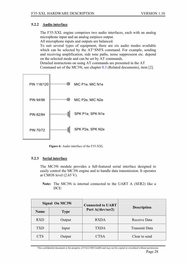
5.2.2 Audio interface
The F35-XXL engine comprises two audio interfaces, each with an analog microphone input and an analog earpiece output. All microphone inputs and outputs are balanced. To suit several types of equipment, there are six audio modes available which can be selected by the AT^SNFS command. For example, sending and receiving amplification, side tone paths, noise suppression etc. depend on the selected mode and can be set by AT commands. Detailed instructions on using AT commands are presented in the AT Command set of the MC39i, see chapter 0.3 (Related documents), item [2].
Figure 6: Audio interface of the F35-XXL
5.2.3 Serial interface
The MC39i module provides a full-featured serial interface designed to easily control the MC39i engine and to handle data transmission. It operates at CMOS level (2.65 V).
Note: The MC39i is internal connected to the UART A (SER2) like a
DCE:
Signal On MC39i
Name Type
Connected to UART Port A(/dev/ser2) Description
RXD Output RXDA Receive Data
TXD Input TXDA Transmit Data
CTS Output CTSA Clear to send
MIC P1e, MIC N1e
MIC P2e, MIC N2e
SPK P1e, SPK N1e
SPK P2e, SPK N2e
PIN 118/120
PIN 94/96
PIN 82/84
PIN 70/72
F35-XXL HARDWARE DESCRIPTION VERSION 1.10
This confidential document is the property of FALCOM GmbH and may not be copied or circulated without permission. Page 29
Signal On MC39i
Name Type
Connected to UART Port A(/dev/ser2) Description
RTS Input RTSA Ready to send
DTR Input DTRA Data Terminal Ready
DSR Output DSRA Data Set Ready
DCD Output DCDA Data Carrier Detect
RI* Output RIA Ring
Table 7: Serial interface of the MC39i
* For more details see chapter “ Ring- ”.
The data interface is implemented as a serial asynchronous transmitter and receiver conforming to ITU-T RS232 Interchange Circuits DCE. It has fixed parameters of 8 data bits, no parity and 1 stop bit and can be selected in the range of 1.2 kbps up to 115 kbps for auto bauding and in the range of 300 baud to 115 kbps for manual settings. Hardware handshake using signals RTS0/CTS0 and software flow control via XON/XOFF are supported. In addition, the modem control signals DTR*), DSR and DCD are available. Different modes of operation can be handled by AT commands. For more information about signal levels of the serial interface see chapter 4.
*) The DTR signal will only be polled once per second from the
internal firmware of MC39i!
5.2.4 Control signals
The following control signals are available (2.65 V CMOS level).
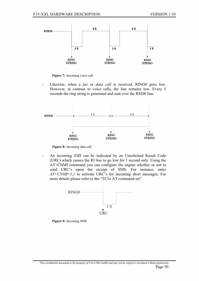
5.2.4.1 Ring- MC39i
The RING0- MC39i pin is connected to the RI-UART pin. The behaviour of the RING0 line depends on the type of the call received.
- When a voice call comes in the RI line goes low for 1 s and high for
another 4 s. Every 5 seconds the ring string is generated and sent over the RXD0 line. If there is a call in progress and call waiting is activated for a connected handset or hands free device, the RING0 witches to ground in order to generate acoustic signals that indicate the waiting call.
F35-XXL HARDWARE DESCRIPTION VERSION 1.10
This confidential document is the property of FALCOM GmbH and may not be copied or circulated without permission. Page 30
Figure 7: Incoming voice call
- Likewise, when a fax or data call is received, RING0 goes low. However, in contrast to voice calls, the line remains low. Every 5 seconds the ring string is generated and sent over the RXD0 line.
Figure 8: Incoming data call - An incoming SMS can be indicated by an Unsolicited Result Code
(URC) which causes the RI line to go low for 1 second only. Using the AT+CNMI command you can configure the engine whether or not to send URC’s upon the receipt of SMS. For instance, enter AT+CNMI=1,1 to activate URC’s for incoming short messages. For more details please refer to the “TC3x AT command set”.
URC
RING0
1 S
Figure 9: Incoming SMS
F35-XXL HARDWARE DESCRIPTION VERSION 1.10
This confidential document is the property of FALCOM GmbH and may not be copied or circulated without permission. Page 31
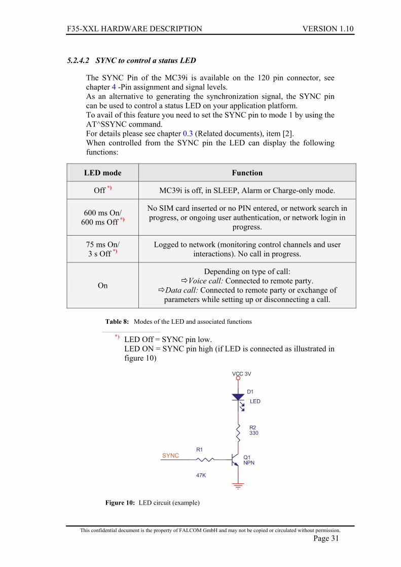
5.2.4.2 SYNC to control a status LED
The SYNC Pin of the MC39i is available on the 120 pin connector, see chapter 4 -Pin assignment and signal levels. As an alternative to generating the synchronization signal, the SYNC pin can be used to control a status LED on your application platform. To avail of this feature you need to set the SYNC pin to mode 1 by using the AT^SSYNC command. For details please see chapter 0.3 (Related documents), item [2]. When controlled from the SYNC pin the LED can display the following functions:
LED mode Function
Off *) MC39i is off, in SLEEP, Alarm or Charge-only mode.
600 ms On/ 600 ms Off *)
No SIM card inserted or no PIN entered, or network search in progress, or ongoing user authentication, or network login in
progress.
75 ms On/ 3 s Off *)
Logged to network (monitoring control channels and user interactions). No call in progress.
On
Depending on type of call: Voice call: Connected to remote party.
Data call: Connected to remote party or exchange of parameters while setting up or disconnecting a call.
Table 8: Modes of the LED and associated functions
*) LED Off = SYNC pin low. LED ON = SYNC pin high (if LED is connected as illustrated in figure 10)
VCC 3V
R1
47K
R2330
Q1NPN
GPIO 1
D1
LED
SYNC
Figure 10: LED circuit (example)
F35-XXL HARDWARE DESCRIPTION VERSION 1.10
This confidential document is the property of FALCOM GmbH and may not be copied or circulated without permission. Page 32
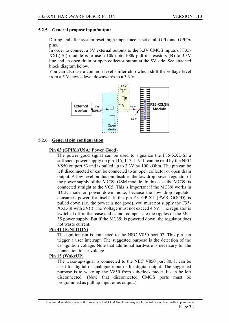
5.2.5 General propose input/output
During and after system reset, high impedance is set at all GPIx and GPIOx pins. In order to connect a 5V external outputs to the 3.3V CMOS inputs of F35-XXL(-SI) module is to use a 10k upto 100k pull up resistors (R) to 3.3V line and an open drain or open collector output at the 5V side. See attached block diagram below. You can also use a common level shifter chip which shift the voltage level from a 5 V device level downwards to a 3.3 V .
5.2.6 General pin configuration
Pin 63 (GPIX1(USA) Power Good) The power good signal can be used to signalize the F35-XXL-SI a sufficient power supply on pin 115, 117, 119. It can be read by the NEC V850 on port 83 and is pulled up to 3.3V by 100 kOhm. The pin can be left disconnected or can be connected to an open collector or open drain output. A low level on this pin disables the low drop power regulator of the power supply of the MC39i GSM module. In this case the MC39i is connected straight to the VC5. This is important if the MC39i works in IDLE mode or power down mode, because the low drop regulator consumes power for itself. If the pin 63 GPIX1 (PWR_GOOD) is pulled down (i.e. the power is not good), you must not supply the F35-XXL-SI with 5V!!! The Voltage must not exceed 4.5V. The regulator is switched off in that case and cannot compensate the ripples of the MC-35 power supply. But if the MC39i is powered down, the regulator does not waste current.
Pin 41 (IGNITION) The ignition pin is connected to the NEC V850 port 07. This pin can trigger a user interrupt. The suggested purpose is the detection of the car ignition voltage. Note that additional hardware is necessary for the connection to car voltage.
Pin 15 (WakeUP) The wake-up-signal is connected to the NEC V850 port 80. It can be used for digital or analogue input or for digital output. The suggested purpose is to wake up the V850 from sub-clock mode. It can be left disconnected. (Note that disconnected CMOS ports must be programmed as pull up input or as output.)
F35-XXL HARDWARE DESCRIPTION VERSION 1.10
This confidential document is the property of FALCOM GmbH and may not be copied or circulated without permission. Page 33
Pin 43 (INTU)
The INTU signal is connected to the NEC V850 port 06. It can trigger a user interrupt. (Note that disconnected CMOS ports must be programmed as pull up input or as output.)
Pin 29 (EMODE) If the e-mode input pin is connected to GND (10 kOhm) the F35-XXL-SI boots from the external FLASH, otherwise it boots from the internal ROM.
Pin 61 (NMI) The NMI pin is connected to the NEC V850 port 00. The NMI can wake up the V850 from the HALT mode. For programming the NMI refer to the NEC manual for the V850/SA1(UPD70F3017AY) hardware.
Pin 106 (BootSel) For normal GPS functionality this pin has to be left open while the GPS-firmware is starting. After the start of the GPS-firmware the pin (106) can be connected to 3.3 V. In that case the first GPS-Port is switched to the pins (98, 100) on the 120-pin connector. In order to reprogram the FLASH of the GPS (e.g. updating a new firmware), this pin (106) has to be set to high (+3.3 V DC) before the internal GPS-firmware is started.
Pin 101 (AVGND) In order to use the analogue inputs, the AVGND pin has to be connected to the reference voltage ground (usual the ground plane near the reference voltage source). To use the GPI1 to GPI8 for analogue input follow the instructions below:
• Connect AVGND to the GND. • Connect AVDD to a voltage up to 4.6V. • Connect AVREF to a reference voltage up to AVDD (2.5V or
2.56, recommended). • See "demo_port_io.c" for software. • Refer to the NEC manual for the V850/SA1(UPD70F3017AY)
hardware. GPS (GPIO’s)
As far as the GPS GPIO’s is concerned, there is no access from the NEC V850 processor. These pins are to be controlled by internal GPS firmware. Unfortunately, the present GPS firmware does not support these pins, but these are depended on the GPS firmware loaded into the GPS FLASH memory.
F35-XXL HARDWARE DESCRIPTION VERSION 1.10
This confidential document is the property of FALCOM GmbH and may not be copied or circulated without permission. Page 34
6 GPS core
6.1 Technical data
FEATURES
- 12 channel GPS receiver
- power consumption: 220 mW (continuous mode with Low Power chipset) 60 mW (trickle power mode)
- protocol: RXA/TXA: NMEA 4800 baud, Msg.: GLL, GGA, RMC, VTG, GSV, GSA, ZDA 8 data bits, no parity, 1 stop bit
RXB/TXB: RTCM, 9600 baud
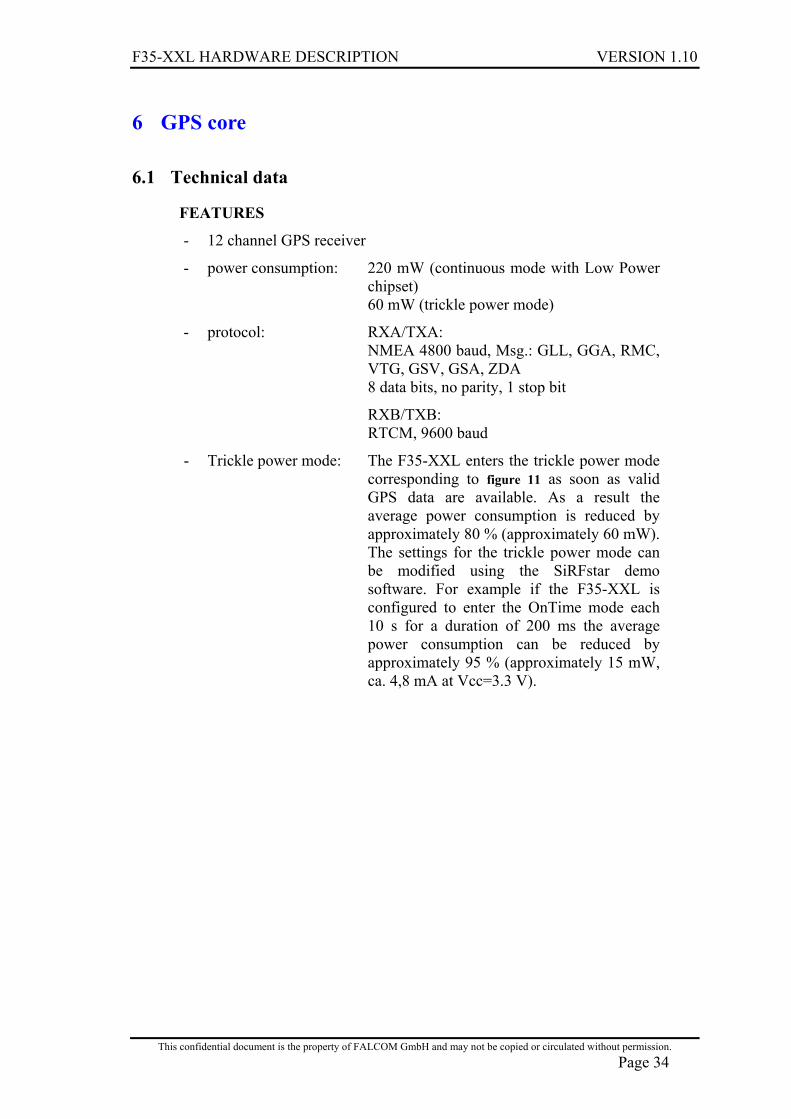
- Trickle power mode: The F35-XXL enters the trickle power mode corresponding to figure 11 as soon as valid GPS data are available. As a result the average power consumption is reduced by approximately 80 % (approximately 60 mW). The settings for the trickle power mode can be modified using the SiRFstar demo software. For example if the F35-XXL is configured to enter the OnTime mode each 10 s for a duration of 200 ms the average power consumption can be reduced by approximately 95 % (approximately 15 mW, ca. 4,8 mA at Vcc=3.3 V).
F35-XXL HARDWARE DESCRIPTION VERSION 1.10
This confidential document is the property of FALCOM GmbH and may not be copied or circulated without permission. Page 35
Figure 11: Default settings for the trickle power mode of F35-XXL
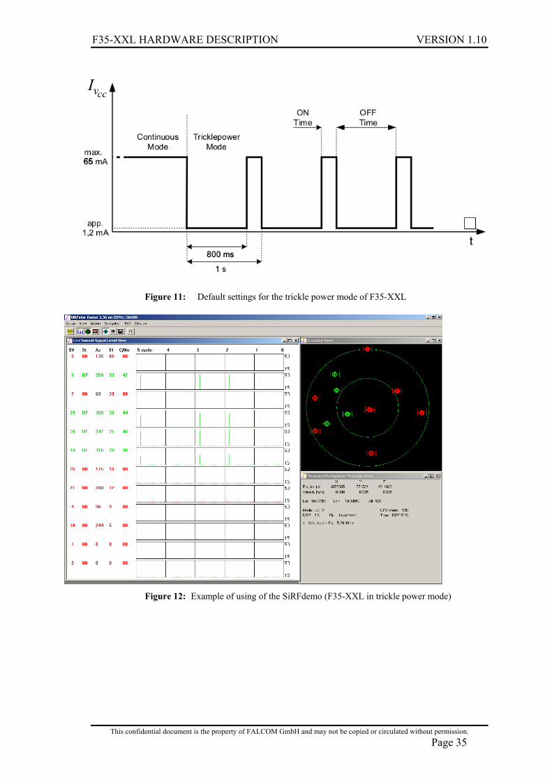
Figure 12: Example of using of the SiRFdemo (F35-XXL in trickle power mode)
F35-XXL HARDWARE DESCRIPTION VERSION 1.10
This confidential document is the property of FALCOM GmbH and may not be copied or circulated without permission. Page 36
6.2 Technical Description
6.2.1 Receiver Architecture
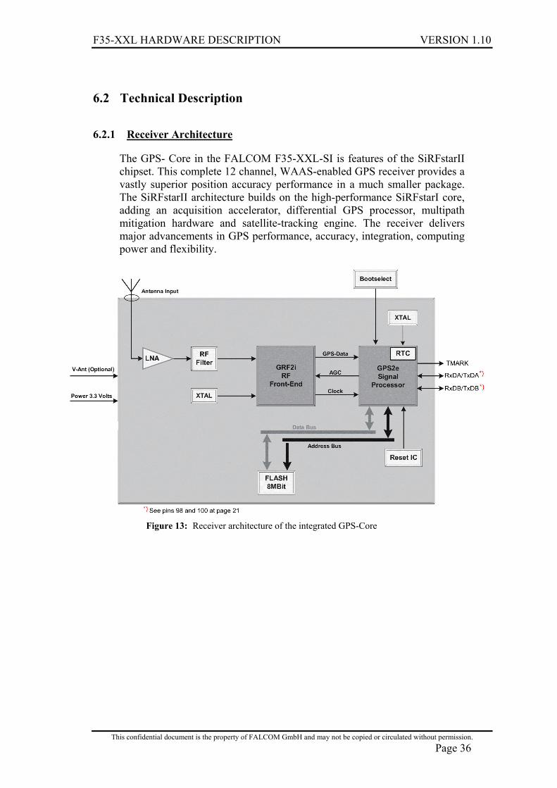
The GPS- Core in the FALCOM F35-XXL-SI is features of the SiRFstarII chipset. This complete 12 channel, WAAS-enabled GPS receiver provides a vastly superior position accuracy performance in a much smaller package. The SiRFstarII architecture builds on the high-performance SiRFstarI core, adding an acquisition accelerator, differential GPS processor, multipath mitigation hardware and satellite-tracking engine. The receiver delivers major advancements in GPS performance, accuracy, integration, computing power and flexibility.
Figure 13: Receiver architecture of the integrated GPS-Core
F35-XXL HARDWARE DESCRIPTION VERSION 1.10
This confidential document is the property of FALCOM GmbH and may not be copied or circulated without permission. Page 37
6.2.2 Technical specification
Electrical Characteristics 1. General
Frequency L1, 1575.42 MHz C/A code 1.023 MHz chip rate Channels 12
2. Accuracy
Position 10 meters CEP without SA Velocity 0.1 meters/second, without SA Time 1 microsecond synchronized to GPS time
3. DGPS Accuracy
Position 1 to 5 meters, typical Velocity 0.05 meters/second, typical
4. Datum
WGS-84
5. Acquisition Rate
Snap start < 3 sec., average Hot start < 8 sec., average Warm start < 38 sec., average Cold start < 45 sec., average
6. Dynamic Conditions
Altitude 18,000 meters (60,000 feet) maxes. Velocity 515 meters/second (1000 knots) max. Acceleration 4 g, max. Jerk 20 meters/second³, max.
7. DC Power
Continuous mode: 65 mA typical Trickle power mode: max. 20 mA
8. Serial Port
Electrical interface See page 21 (GPS)
F35-XXL HARDWARE DESCRIPTION VERSION 1.10
This confidential document is the property of FALCOM GmbH and may not be copied or circulated without permission. Page 38
Protocol messages SiRF binary and NMEA-0183, version 2.20 with a baud rate selection SiRF binary – position, velocity, altitude, status and control NMEA – CGA, GLL, GSA, GSV, RMC and VTG
DGPS protocol RTCM SC-104, version 2.00, type 1, 5 and 9
9. Time – 1PPS Pulse
Level CMOS Pulse duration 100 ms Time reference at the pulse positive edge Measurements Aligned to GPS second, ± microsecond
6.3 Hardware Interface
6.3.1 Configuration and timing signals
Bootselect (Pin 106) Set this Pin to high for programming the flash of the GPS core (for instance updating to a new firmware for the GPS core).
6.3.2 Serial communication signals
The board supports one of two full duplex serial channels. The connections are at CMOS levels, all support variable baud rates and all can be controlled from the appropriate screens in SiRFdemo software. You can directly communicate with a PC serial port. Pins below are depended from status of UPDATE_GPS (pin 106), see table on page 21. RxDA (Pin 98) This is the main receiving channel (GPS port A)
and is used to receive software commands to the board from SiRFdemo software or from user written software. This pin can be available for use on the boar-to-board connector, if the UPDATE_GPS (pin 106) is driven to HIGH level (3.3 V)
RxDB (Pin 98) This is the auxiliary receiving channel (GPS port B) and is used to input differential corrections to the board to enable DGPS navigation. This pin can be available for use on the boar-to-board connector, if the UPDATE_GPS (pin 106) is left open (default setting).
TxDA (Pin 100) This is the main transmitting channel (GPS port A) and is used to output navigation and measurement data to SiRFdemo or user written software. This pin can be available for use on the boar-to-board
F35-XXL HARDWARE DESCRIPTION VERSION 1.10
This confidential document is the property of FALCOM GmbH and may not be copied or circulated without permission. Page 39
connector, if the UPDATE_GPS (pin 106) is driven to HIGH level (3.3 V).
TxDB (Pin 100) For user’s application. This pin (GPS port B) can be available for use on the boar-to-board connector, if the UPDATE_GPS (pin 106) is left open (default setting).
F35-XXL HARDWARE DESCRIPTION VERSION 1.10
This confidential document is the property of FALCOM GmbH and may not be copied or circulated without permission. Page 40
6.3.3 DC input signals
6.3.4 General purpose input/output (pin 81, 110, 112, 114 and 116)
Several I/O’s of the CPU are connected to the hardware interface connector of the MC39i. They are reserved for customer specific applications.
6.4 Software interface
The GPS-Receiver in the MC39i supports NMEA-0183 and SiRF binary protocols. A short description of these protocols is provided herein. For more detailed information please refer to the SiRFstarII message set specification available in the section “/service/downloads/manuals/SiRF” of the FALCOM homepage.
F35-XXL HARDWARE DESCRIPTION VERSION 1.10
This confidential document is the property of FALCOM GmbH and may not be copied or circulated without permission. Page 41
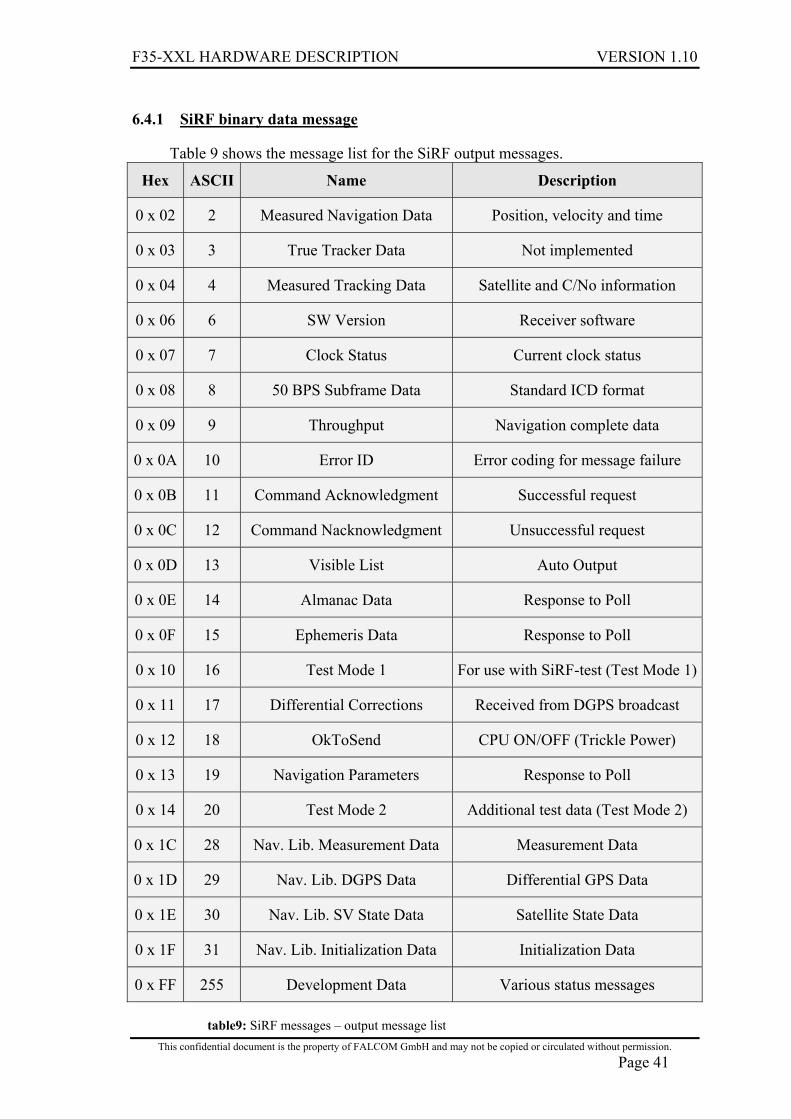
6.4.1 SiRF binary data message
Table 9 shows the message list for the SiRF output messages.
Hex ASCII Name Description
0 x 02 2 Measured Navigation Data Position, velocity and time
0 x 03 3 True Tracker Data Not implemented
0 x 04 4 Measured Tracking Data Satellite and C/No information
0 x 06 6 SW Version Receiver software
0 x 07 7 Clock Status Current clock status
0 x 08 8 50 BPS Subframe Data Standard ICD format
0 x 09 9 Throughput Navigation complete data
0 x 0A 10 Error ID Error coding for message failure
0 x 0B 11 Command Acknowledgment Successful request
0 x 0C 12 Command Nacknowledgment Unsuccessful request
0 x 0D 13 Visible List Auto Output
0 x 0E 14 Almanac Data Response to Poll
0 x 0F 15 Ephemeris Data Response to Poll
0 x 10 16 Test Mode 1 For use with SiRF-test (Test Mode 1)
0 x 11 17 Differential Corrections Received from DGPS broadcast
0 x 12 18 OkToSend CPU ON/OFF (Trickle Power)
0 x 13 19 Navigation Parameters Response to Poll
0 x 14 20 Test Mode 2 Additional test data (Test Mode 2)
0 x 1C 28 Nav. Lib. Measurement Data Measurement Data
0 x 1D 29 Nav. Lib. DGPS Data Differential GPS Data
0 x 1E 30 Nav. Lib. SV State Data Satellite State Data
0 x 1F 31 Nav. Lib. Initialization Data Initialization Data
0 x FF 255 Development Data Various status messages table9: SiRF messages – output message list
F35-XXL HARDWARE DESCRIPTION VERSION 1.10
This confidential document is the property of FALCOM GmbH and may not be copied or circulated without permission. Page 42
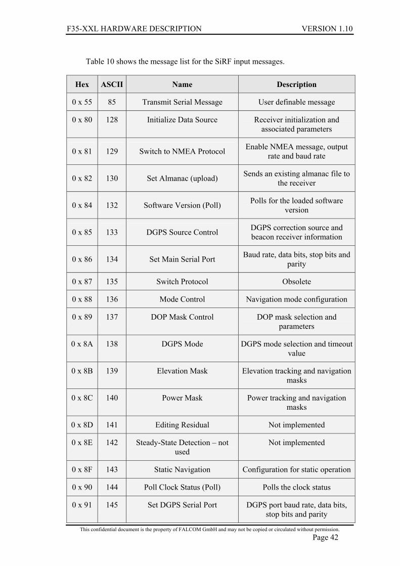
Table 10 shows the message list for the SiRF input messages.
Hex ASCII Name Description
0 x 55 85 Transmit Serial Message User definable message
0 x 80 128 Initialize Data Source Receiver initialization and associated parameters
0 x 81 129 Switch to NMEA Protocol Enable NMEA message, output rate and baud rate
0 x 82 130 Set Almanac (upload) Sends an existing almanac file to the receiver
0 x 84 132 Software Version (Poll) Polls for the loaded software version
0 x 85 133 DGPS Source Control DGPS correction source and beacon receiver information
0 x 86 134 Set Main Serial Port Baud rate, data bits, stop bits and parity
0 x 87 135 Switch Protocol Obsolete
0 x 88 136 Mode Control Navigation mode configuration
0 x 89 137 DOP Mask Control DOP mask selection and parameters
0 x 8A 138 DGPS Mode DGPS mode selection and timeout value
0 x 8B 139 Elevation Mask Elevation tracking and navigation masks
0 x 8C 140 Power Mask Power tracking and navigation masks
0 x 8D 141 Editing Residual Not implemented
0 x 8E 142 Steady-State Detection – not used
Not implemented
0 x 8F 143 Static Navigation Configuration for static operation
0 x 90 144 Poll Clock Status (Poll) Polls the clock status
0 x 91 145 Set DGPS Serial Port DGPS port baud rate, data bits, stop bits and parity
F35-XXL HARDWARE DESCRIPTION VERSION 1.10
This confidential document is the property of FALCOM GmbH and may not be copied or circulated without permission. Page 43
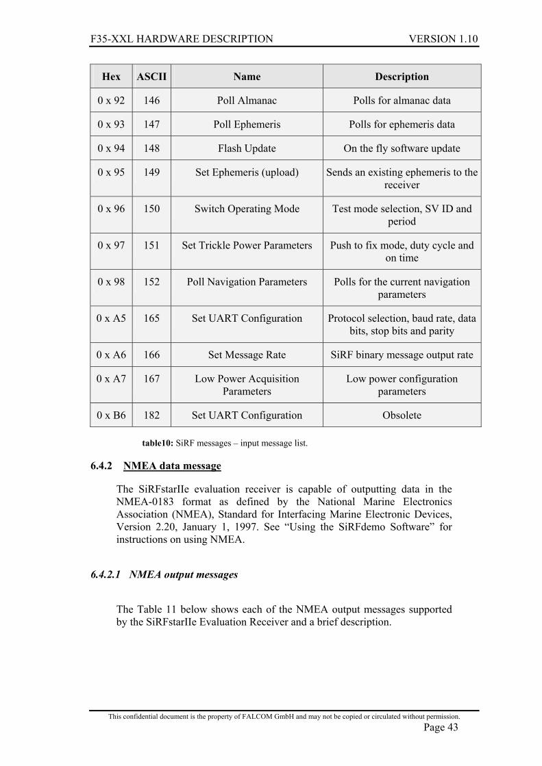
Hex ASCII Name Description
0 x 92 146 Poll Almanac Polls for almanac data
0 x 93 147 Poll Ephemeris Polls for ephemeris data
0 x 94 148 Flash Update On the fly software update
0 x 95 149 Set Ephemeris (upload) Sends an existing ephemeris to the receiver
0 x 96 150 Switch Operating Mode Test mode selection, SV ID and period
0 x 97 151 Set Trickle Power Parameters Push to fix mode, duty cycle and on time
0 x 98 152 Poll Navigation Parameters Polls for the current navigation parameters
0 x A5 165 Set UART Configuration Protocol selection, baud rate, data bits, stop bits and parity
0 x A6 166 Set Message Rate SiRF binary message output rate
0 x A7 167 Low Power Acquisition Parameters
Low power configuration parameters
0 x B6 182 Set UART Configuration Obsolete table10: SiRF messages – input message list.
6.4.2 NMEA data message
The SiRFstarIIe evaluation receiver is capable of outputting data in the NMEA-0183 format as defined by the National Marine Electronics Association (NMEA), Standard for Interfacing Marine Electronic Devices, Version 2.20, January 1, 1997. See “Using the SiRFdemo Software” for instructions on using NMEA.
6.4.2.1 NMEA output messages
The Table 11 below shows each of the NMEA output messages supported by the SiRFstarIIe Evaluation Receiver and a brief description.
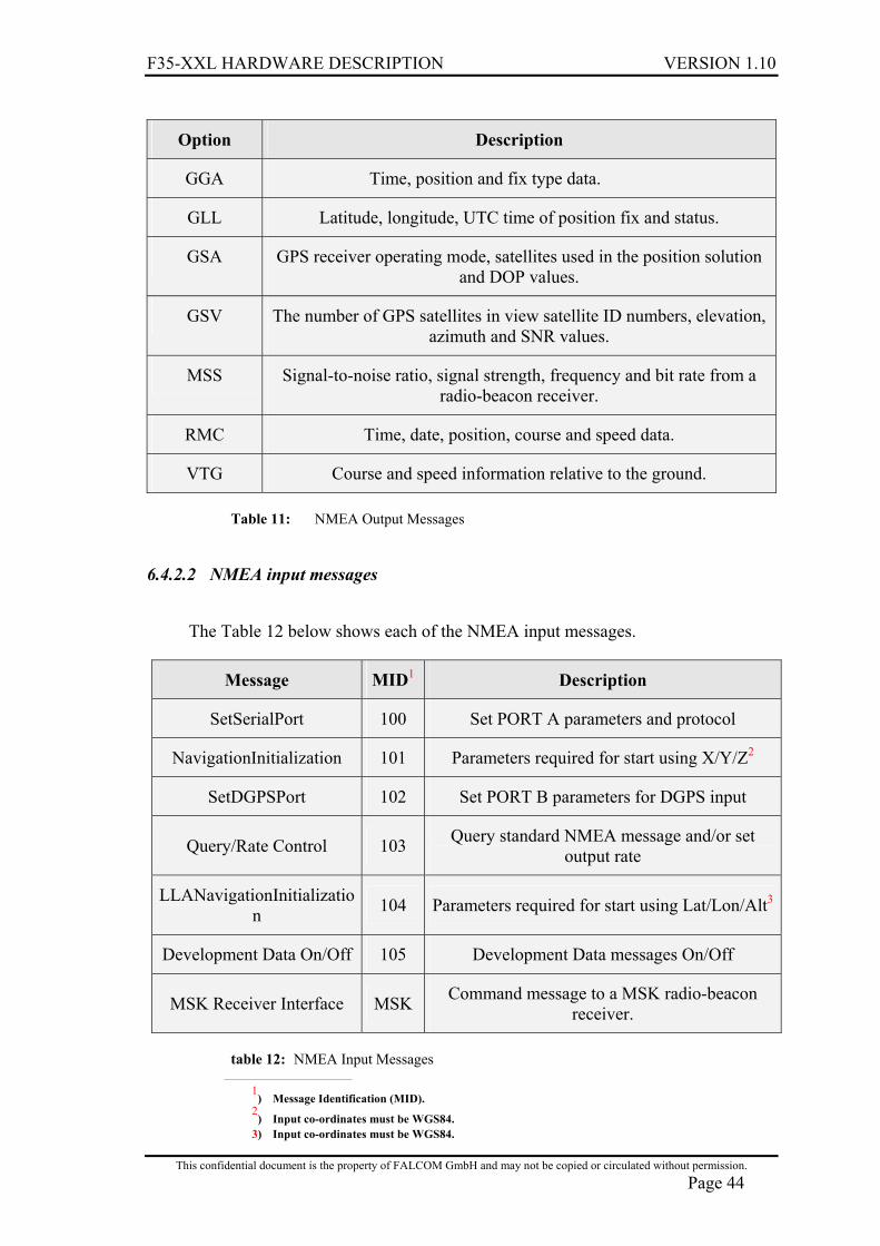
F35-XXL HARDWARE DESCRIPTION VERSION 1.10
This confidential document is the property of FALCOM GmbH and may not be copied or circulated without permission. Page 44
Option Description
GGA Time, position and fix type data.
GLL Latitude, longitude, UTC time of position fix and status.
GSA GPS receiver operating mode, satellites used in the position solution and DOP values.
GSV The number of GPS satellites in view satellite ID numbers, elevation, azimuth and SNR values.
MSS Signal-to-noise ratio, signal strength, frequency and bit rate from a radio-beacon receiver.
RMC Time, date, position, course and speed data.
VTG Course and speed information relative to the ground.
Table 11: NMEA Output Messages
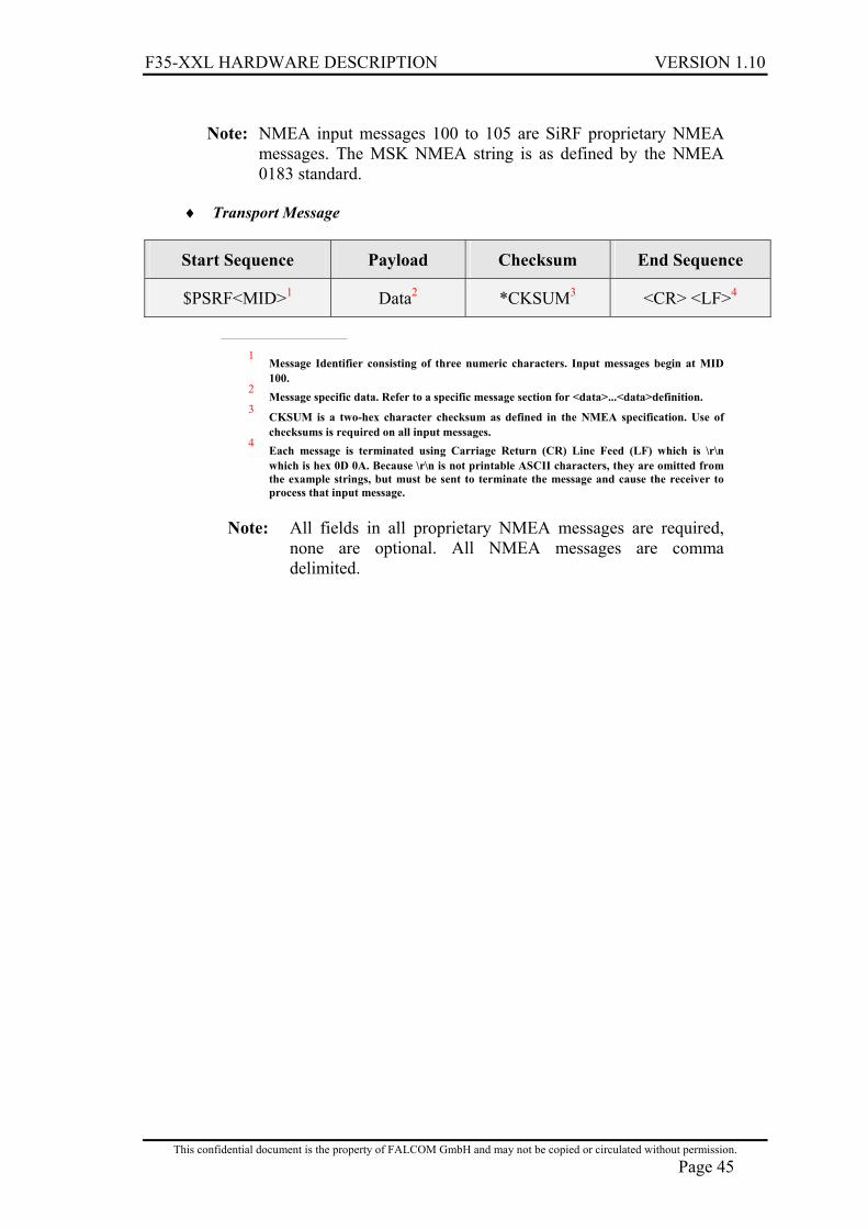
6.4.2.2 NMEA input messages
The Table 12 below shows each of the NMEA input messages.
Message MID1 Description
SetSerialPort 100 Set PORT A parameters and protocol
NavigationInitialization 101 Parameters required for start using X/Y/Z2
SetDGPSPort 102 Set PORT B parameters for DGPS input
Query/Rate Control 103 Query standard NMEA message and/or set output rate
LLANavigationInitialization 104 Parameters required for start using Lat/Lon/Alt3
Development Data On/Off 105 Development Data messages On/Off
MSK Receiver Interface MSK Command message to a MSK radio-beacon receiver.
table 12: NMEA Input Messages
1) Message Identification (MID).
2) Input co-ordinates must be WGS84.
3) Input co-ordinates must be WGS84.
F35-XXL HARDWARE DESCRIPTION VERSION 1.10
This confidential document is the property of FALCOM GmbH and may not be copied or circulated without permission. Page 45
Note: NMEA input messages 100 to 105 are SiRF proprietary NMEA
messages. The MSK NMEA string is as defined by the NMEA 0183 standard.
♦ Transport Message
Start Sequence Payload Checksum End Sequence
$PSRF<MID>1 Data2 *CKSUM3 <CR> <LF>4
1
Message Identifier consisting of three numeric characters. Input messages begin at MID 100.
2 Message specific data. Refer to a specific message section for <data>...<data>definition.
3 CKSUM is a two-hex character checksum as defined in the NMEA specification. Use of checksums is required on all input messages.
4 Each message is terminated using Carriage Return (CR) Line Feed (LF) which is \r\n which is hex 0D 0A. Because \r\n is not printable ASCII characters, they are omitted from the example strings, but must be sent to terminate the message and cause the receiver to process that input message.
Note: All fields in all proprietary NMEA messages are required,
none are optional. All NMEA messages are comma delimited.
F35-XXL HARDWARE DESCRIPTION VERSION 1.10
This confidential document is the property of FALCOM GmbH and may not be copied or circulated without permission. Page 46
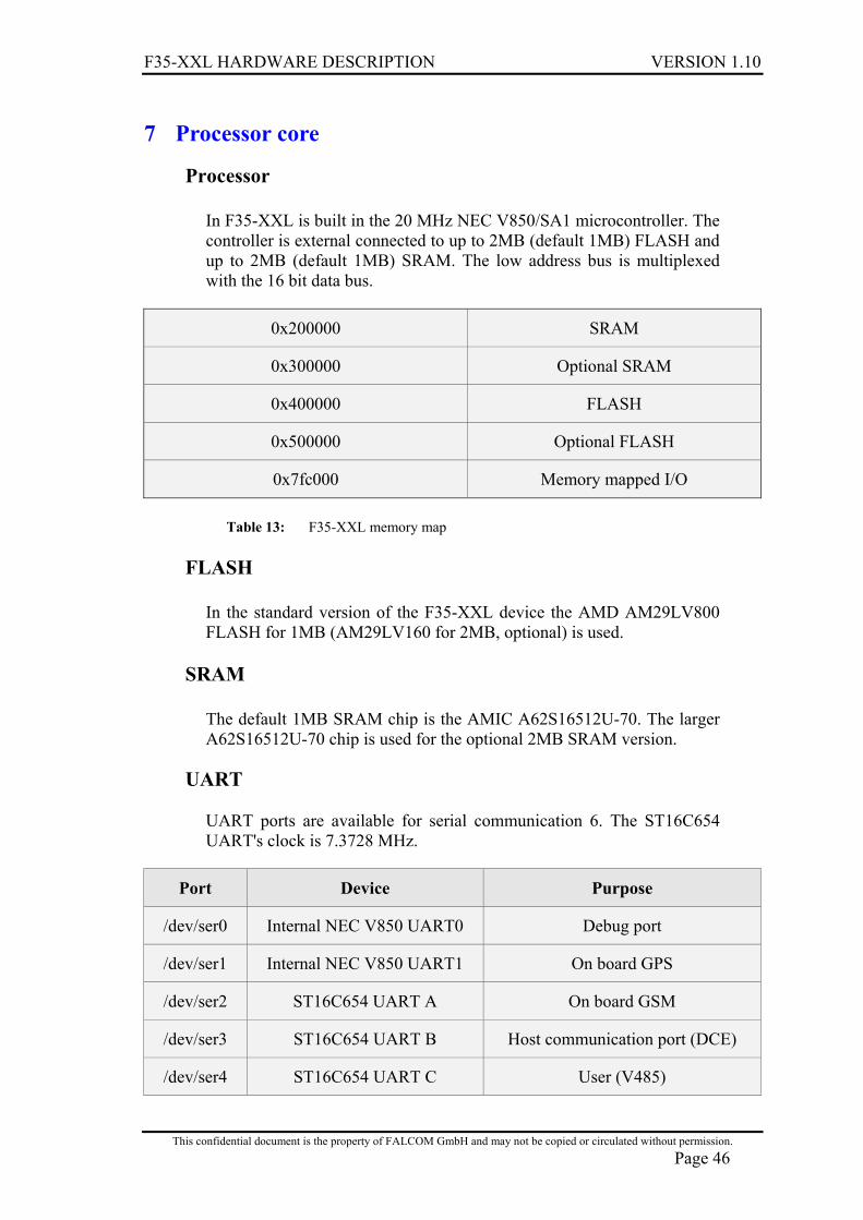
7 Processor core
Processor
In F35-XXL is built in the 20 MHz NEC V850/SA1 microcontroller. The controller is external connected to up to 2MB (default 1MB) FLASH and up to 2MB (default 1MB) SRAM. The low address bus is multiplexed with the 16 bit data bus.
0x200000 SRAM
0x300000 Optional SRAM
0x400000 FLASH
0x500000 Optional FLASH
0x7fc000 Memory mapped I/O
Table 13: F35-XXL memory map
FLASH
In the standard version of the F35-XXL device the AMD AM29LV800 FLASH for 1MB (AM29LV160 for 2MB, optional) is used.
SRAM
The default 1MB SRAM chip is the AMIC A62S16512U-70. The larger A62S16512U-70 chip is used for the optional 2MB SRAM version.
UART
UART ports are available for serial communication 6. The ST16C654 UART's clock is 7.3728 MHz.
Port Device Purpose
/dev/ser0 Internal NEC V850 UART0 Debug port
/dev/ser1 Internal NEC V850 UART1 On board GPS
/dev/ser2 ST16C654 UART A On board GSM
/dev/ser3 ST16C654 UART B Host communication port (DCE)
/dev/ser4 ST16C654 UART C User (V485)
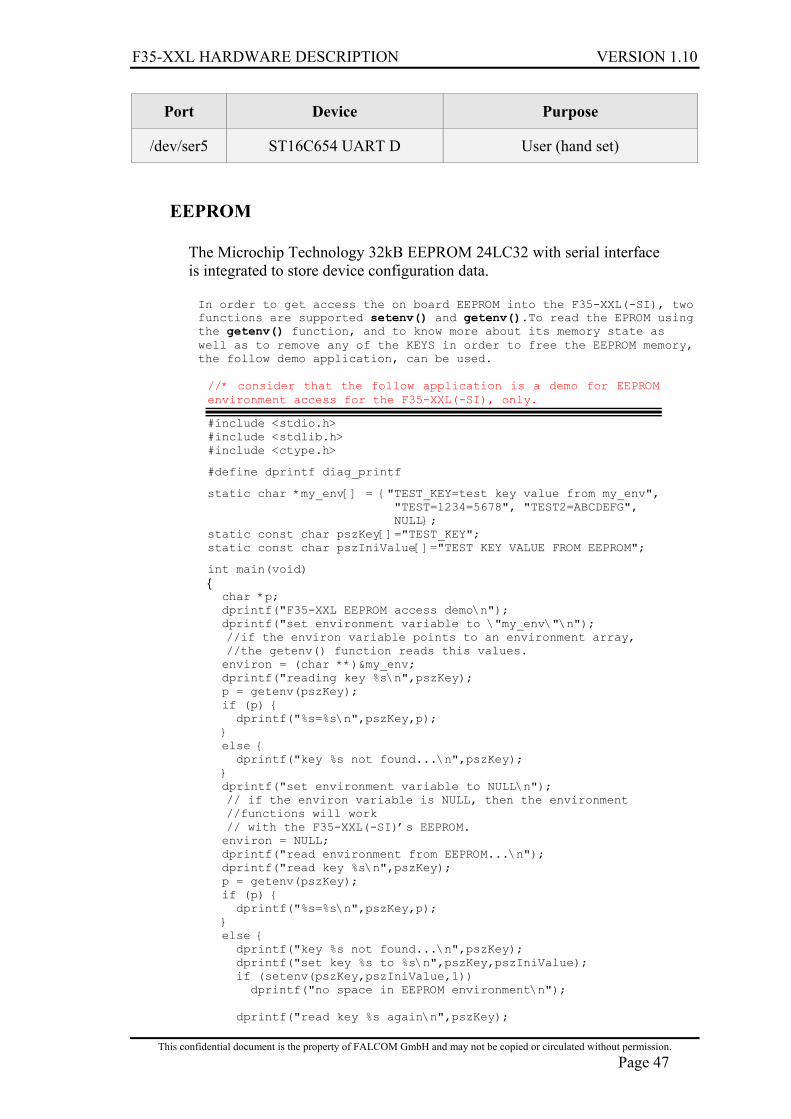
F35-XXL HARDWARE DESCRIPTION VERSION 1.10
This confidential document is the property of FALCOM GmbH and may not be copied or circulated without permission. Page 47
Port Device Purpose
/dev/ser5 ST16C654 UART D User (hand set)
EEPROM
The Microchip Technology 32kB EEPROM 24LC32 with serial interface is integrated to store device configuration data. In order to get access the on board EEPROM into the F35-XXL(-SI), two functions are supported setenv() and getenv().To read the EPROM using the getenv() function, and to know more about its memory state as well as to remove any of the KEYS in order to free the EEPROM memory, the follow demo application, can be used. //* consider that the follow application is a demo for EEPROM environment access for the F35-XXL(-SI), only.
#include <stdio.h> #include <stdlib.h> #include <ctype.h>
#define dprintf diag_printf
static char *my_env[] = "TEST_KEY=test key value from my_env", "TEST=1234=5678", "TEST2=ABCDEFG", NULL; static const char pszKey[]="TEST_KEY"; static const char pszIniValue[]="TEST KEY VALUE FROM EEPROM";
int main(void) char *p; dprintf("F35-XXL EEPROM access demo\n"); dprintf("set environment variable to \"my_env\"\n");
//if the environ variable points to an environment array, //the getenv() function reads this values.
environ = (char **)&my_env; dprintf("reading key %s\n",pszKey); p = getenv(pszKey); if (p) dprintf("%s=%s\n",pszKey,p); else dprintf("key %s not found...\n",pszKey); dprintf("set environment variable to NULL\n");
// if the environ variable is NULL, then the environment //functions will work // with the F35-XXL(-SI)’s EEPROM.
environ = NULL; dprintf("read environment from EEPROM...\n"); dprintf("read key %s\n",pszKey); p = getenv(pszKey); if (p) dprintf("%s=%s\n",pszKey,p); else dprintf("key %s not found...\n",pszKey); dprintf("set key %s to %s\n",pszKey,pszIniValue); if (setenv(pszKey,pszIniValue,1)) dprintf("no space in EEPROM environment\n"); dprintf("read key %s again\n",pszKey);
F35-XXL HARDWARE DESCRIPTION VERSION 1.10
This confidential document is the property of FALCOM GmbH and may not be copied or circulated without permission. Page 48
p = getenv(pszKey); if (p) dprintf("%s=%s\n",pszKey,p); else dprintf("key %s not found.\n",pszKey); dprintf("remove key %s\n",pszKey); unsetenv(pszKey); dprintf("read key %s\n",pszKey); p = getenv(pszKey); if (p) dprintf("key not removed %s=%s\n",pszKey,p); else dprintf("key %s removed.\n",pszKey); dprintf("exit EEPROM access demo\n"); return 0;
RTC
The PCF8593 real time clock is a low-power clock/calendar with 2-wire serial bus connection to the NEC V850 controller.
Reset/watch dog
The supervisor chip MAX6366 realises the power on reset and watches dog functionality. After reset the watch dog is automatically triggered by the CPLD. After the first software trigger the watch dog is active and must be triggered 1 time per 500 ms or faster.
The hardware watchdog chip MAX6366 is part of the F35-XXL(-SI).The timeout period is between 1 second and 2.25 seconds. Without a trigger signal the device performs a reset after this time. The watchdog is triggered by input or output on the address 0x3FFFF8. The sequence for disabling the watchdog is: write-read-write-write-read-write-write-write (write the value 0xE5 to the address 0x3FFFF8 ) The next input or output on 0x3FFFF8 enables the watchdog. A watchdog device is available in eCos. Insert it with "ecosconfig add watchdog".
#include <stdio.h> // printf #include <cyg/kernel/kapi.h> // cyg_thread_delay #include <cyg/io/watchdog.hxx> // watchdog class int main() int i; printf("starting watchdog\n"); Cyg_Watchdog::watchdog.start(); Cyg_Watchdog::watchdog.reset(); for (i=0;i<10;i++) Cyg_Watchdog::watchdog.reset(); printf("beating watchdog %d\n",i); cyg_thread_delay(100); Cyg_Watchdog::watchdog.stop(); printf("watchdog stopped\ntesting for reset\n");
F35-XXL HARDWARE DESCRIPTION VERSION 1.10
This confidential document is the property of FALCOM GmbH and may not be copied or circulated without permission. Page 49
for (i=0;i<10;i++) cyg_thread_delay(100); printf("waiting %d\n", 10-i); Cyg_Watchdog::watchdog.start();
printf("watchdog started argain\nwaiting for hardware reset...\n");
for (i=0;i<10;i++) cyg_thread_delay(100); printf("waiting %d\n", 10-i); printf("watchdog doesn't reset hardware!!!\n"); return 0; ;
CPLD
The XCR3032XL-7VQ44C decodes I/O addresses and triggers the watch dog. This chip is on board user programmable. • For more information about XCR3032XL-7VQ44C- Chipset
programmable see page 20 (JTAG pins 52,54,57 and 86) and please visit the internet Homepage http://www.xilinx.com/
In order to use the on-board Xilinx CPLD the JTAG interface is usable for it, only. All the 32 macro-cells are used for basic functionality: - address decoding for RAM, FLASH, UART and user chip select signals. - auto trigger function for the watchdog
There are no more resources available on it. You can attach hardware to the F35-XXL-SI's V850-SA1 processor bus. The address and data bus is multiplexed. You can use the PLD_IO1 to PLD_IO4 as user chip select signals. The addresses for I/O are:
PLD_IO1 0x3fd400 (0x7fd400 with waite state) PLD_IO2 0x3fd800 (0x7fd800 with waite state) PLD_IO3 0x3fdc00 (0x7fdc00 with waite state) PLD_IO4 0x3fe000 (0x7fe000 with waite state)
The VHDL code for the address decoder of the F35-XXL-SI REV 02D is:
---------------------------------------------------------------------------- -- 22 1111 1111 1100 0000 0000 -- 10 9876 5432 1098 7654 3210 -- Flash 0a aaaa aaaa aaaa aaaa axxx -- RAM Select 1n nnnn naaa aaaa aaaa axxx -- COM(3) 11 1111 1100 00aa aaaa axxx 3fc000 -- COM(4) 11 1111 1100 01aa aaaa axxx 3fc400 -- COM(5) 11 1111 1100 10aa aaaa axxx 3fc800 -- COM(6) 11 1111 1100 11aa aaaa axxx 3fcc00 -- OUT_CSIO(0) (NC) 11 1111 1101 00aa aaaa axxx 3fd000 -- OUT_CSIO(1) (PLD_IO1) 11 1111 1101 01aa aaaa axxx 3fd400 -- OUT_CSIO(2) (PLD_IO2) 11 1111 1101 10aa aaaa axxx 3fd800 -- OUT_CSIO(3) (PLD_IO3) 11 1111 1101 11aa aaaa axxx 3fdc00 -- OUT_CSIO(4) (PLD_IO4) 11 1111 1110 00aa aaaa axxx 3fe000 -- WDOG 11 1111 1111 11aa aaaa axxx 3ffff8 -- Flash FCE <= A(21); -- RAM Select RCE <= NOT ( A(21) AND NOT(A(20) and A(19)and A(18)and A(17)and A(16)and
AD(15)and AD(14))); -- Serial CSCOM(3) <= NOT (A(21) and A(20) and A(19)and A(18)and A(17)and A(16)and
A(15)and A(14)and not A(13)and not A(12)and not A(11)and not A(10));
F35-XXL HARDWARE DESCRIPTION VERSION 1.10
This confidential document is the property of FALCOM GmbH and may not be copied or circulated without permission. Page 50
CSCOM(4) <= NOT (A(21) and A(20) and A(19)and A(18)and A(17)and A(16)and A(15)and A(14)and not A(13)and not A(12)and not A(11)and A(10));
CSCOM(5) <= NOT (A(21) and A(20) and A(19)and A(18)and A(17)and A(16)and A(15)and A(14)and not A(13)and not A(12)and A(11)and not A(10));
CSCOM(6) <= NOT (A(21) and A(20) and A(19)and A(18)and A(17)and A(16)and A(15)and A(14)and not A(13)and not A(12)and A(11)and A(10));
-- CSIO CSIO(0) <= DSTRB or NOT (A(21) and A(20) and A(19)and A(18)and A(17)and
A(16)and A(15)and A(14)and not A(13)and A(12)and not A(11)and A(10)); CSIO(1) <= DSTRB or NOT (A(21) and A(20) and A(19)and A(18)and A(17)and
A(16)and A(15)and A(14)and not A(13)and A(12)and not A(11)and A(10)); CSIO(2) <= DSTRB or NOT (A(21) and A(20) and A(19)and A(18)and A(17)and
A(16)and A(15)and A(14)and not A(13)and A(12)and A(11)and not A(10)); CSIO(3) <= DSTRB or NOT (A(21) and A(20) and A(19)and A(18)and A(17)and
A(16)and A(15)and A(14)and not A(13)and A(12)and A(11)and A(10)); CSIO(4) <= DSTRB or NOT (A(21) and A(20) and A(19)and A(18)and A(17)and
A(16)and A(15)and A(14)and A(13)and not A(12)and not A(11)and not A(10));
-- CS_WDOG CS_WDOG <= not DSTRB and A(21) and A(20) and A(19)and A(18)and A(17)and
A(16)and A(15)and A(14)and A(13)and A(12)and A(11) and A(10); -------------------------------------------------------------------------
7.1 How to use the TCP/IP and PPP stack
The eCos 1.3 TCP/IP stack is running without PPP. The tcp/ip + ppp stack we shipped is a special designed stack for a very small environments and was ported on the F35-XXL(-SI). This stack includes 3-rd party license (sevenstax), so we can only ship object code in normal and debug versions. The updated “tcp.tgz” package can be found on our homepage under "http://www.falcom.de/pub/f35-xxl/index.html"
- the most problems that have been occured, are while dialing into a network service provider via GPRS.
- we see that each provider uses its own derivate of PPP - so please notice: try to get all information on PPP authorization from your chosen
provider. test different providers in your country and let us know with which
one it works and where not. we are not able to test it from our side, because we don't have your
network! we also can not simulate this network if we don't know the settings of the chosen provider please provide the whole logging data to FALCOM for initial analysis we can give you a TCP/IP and PPP stack as it is in object code - if you need "special changes or support" you should contact
"Sevenstax" Notice: The special changes or support from Sevenstax is not for
free - they offer training, application, support for TCP/IP and PPP
F35-XXL HARDWARE DESCRIPTION VERSION 1.10
This confidential document is the property of FALCOM GmbH and may not be copied or circulated without permission. Page 51
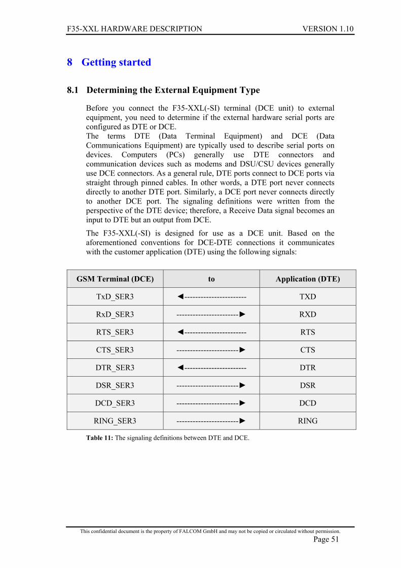
8 Getting started
8.1 Determining the External Equipment Type
Before you connect the F35-XXL(-SI) terminal (DCE unit) to external equipment, you need to determine if the external hardware serial ports are configured as DTE or DCE. The terms DTE (Data Terminal Equipment) and DCE (Data Communications Equipment) are typically used to describe serial ports on devices. Computers (PCs) generally use DTE connectors and communication devices such as modems and DSU/CSU devices generally use DCE connectors. As a general rule, DTE ports connect to DCE ports via straight through pinned cables. In other words, a DTE port never connects directly to another DTE port. Similarly, a DCE port never connects directly to another DCE port. The signaling definitions were written from the perspective of the DTE device; therefore, a Receive Data signal becomes an input to DTE but an output from DCE.
The F35-XXL(-SI) is designed for use as a DCE unit. Based on the aforementioned conventions for DCE-DTE connections it communicates with the customer application (DTE) using the following signals:
GSM Terminal (DCE) to Application (DTE)
TxD_SER3 ----------------------- TXD
RxD_SER3 ----------------------- RXD
RTS_SER3 ----------------------- RTS
CTS_SER3 ----------------------- CTS
DTR_SER3 ----------------------- DTR
DSR_SER3 ----------------------- DSR
DCD_SER3 ----------------------- DCD
RING_SER3 ----------------------- RING
Table 11: The signaling definitions between DTE and DCE.
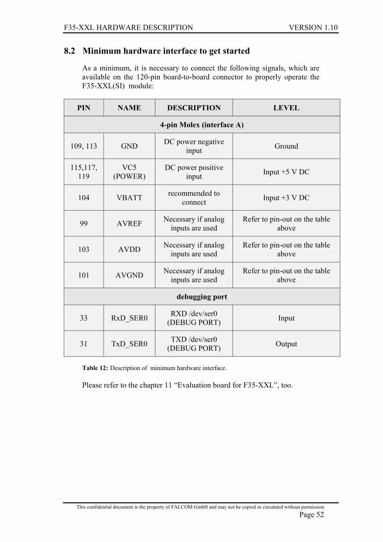
F35-XXL HARDWARE DESCRIPTION VERSION 1.10
This confidential document is the property of FALCOM GmbH and may not be copied or circulated without permission. Page 52
8.2 Minimum hardware interface to get started
As a minimum, it is necessary to connect the following signals, which are available on the 120-pin board-to-board connector to properly operate the F35-XXL(SI) module:
PIN NAME DESCRIPTION LEVEL
4-pin Molex (interface A)
109, 113 GND DC power negative input Ground
115,117, 119
VC5 (POWER)
DC power positive input Input +5 V DC
104 VBATT recommended to connect Input +3 V DC
99 AVREF Necessary if analog inputs are used
Refer to pin-out on the table above
103 AVDD Necessary if analog inputs are used
Refer to pin-out on the table above
101 AVGND Necessary if analog inputs are used
Refer to pin-out on the table above
debugging port
33 RxD_SER0 RXD /dev/ser0 (DEBUG PORT) Input
31 TxD_SER0 TXD /dev/ser0 (DEBUG PORT) Output
Table 12: Description of minimum hardware interface. Please refer to the chapter 11 “Evaluation board for F35-XXL”, too.
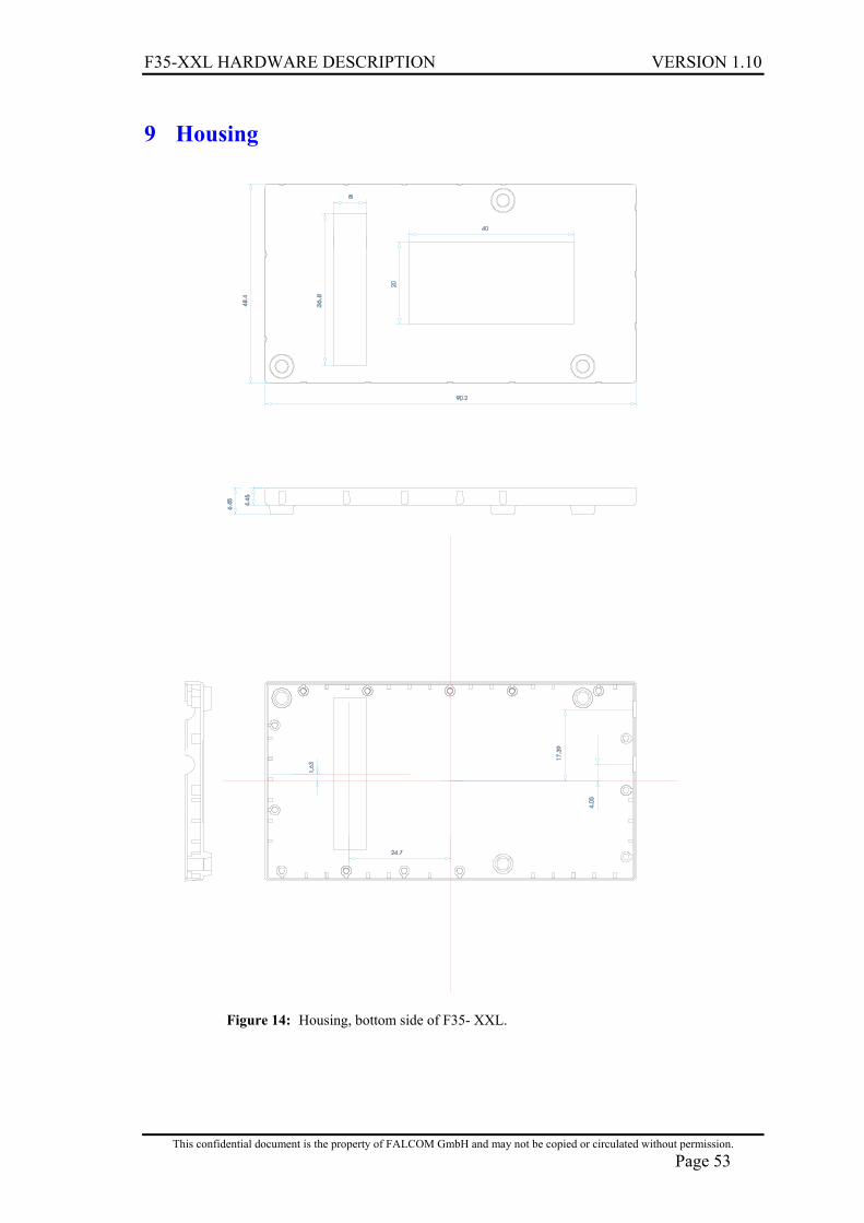
F35-XXL HARDWARE DESCRIPTION VERSION 1.10
This confidential document is the property of FALCOM GmbH and may not be copied or circulated without permission. Page 53
9 Housing
Figure 14: Housing, bottom side of F35- XXL.
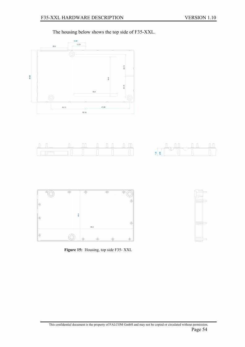
F35-XXL HARDWARE DESCRIPTION VERSION 1.10
This confidential document is the property of FALCOM GmbH and may not be copied or circulated without permission. Page 54
The housing below shows the top side of F35-XXL.
Figure 15: Housing, top side F35- XXL
F35-XXL HARDWARE DESCRIPTION VERSION 1.10
This confidential document is the property of FALCOM GmbH and may not be copied or circulated without permission. Page 55
10 EMC and ESD requirement
The ETS 300342-1 standard applies to the F35-XXL with regard to EMC and ESD requirements.
Additional requirements in relation to EMC/ESD:
- If the F35-XXL is being used in cars, the requirements regarding power
supply as defined in section 9.6 of the ETS 300342-1 (6/97) standard must be fulfilled.
- The length of the connecting cable to the 120pin interface must be less
than 2m; otherwise, measurements must be carried out in compliance with section 9.5 of the ETS 300 342-1 (6/97) standard.
- The connecting cable between the chip card reader and the socket on
the F35-XXL must be shielded in compliance with EMC requirements. - When using the F35-XXL cellular engine with individual hands free
equipment, noise interference may occur. - The F35-XXL cellular engine must be connected directly to the ground
of the base device.
Note: The device should only be handled in compliance with ESD regulations (grounded, ESD chain, trained personnel).
F35-XXL HARDWARE DESCRIPTION VERSION 1.10
This confidential document is the property of FALCOM GmbH and may not be copied or circulated without permission. Page 56
11 CE conformity
The F35-XXL bears the CE symbol. This symbol represents the manufacturer’s declaration that the design and implementation of the F35-XXL meets the currently valid versions of the following.
- EU guidelines:
89/336/EC (EMC guideline) 73/23/EC (Low voltage guideline) 91/263/EC (Telecommunication devices guideline)
- Standards:
EMC: ETS 300342-1 Safety: EN 60950 GSM network: TBR 19
TBR 20
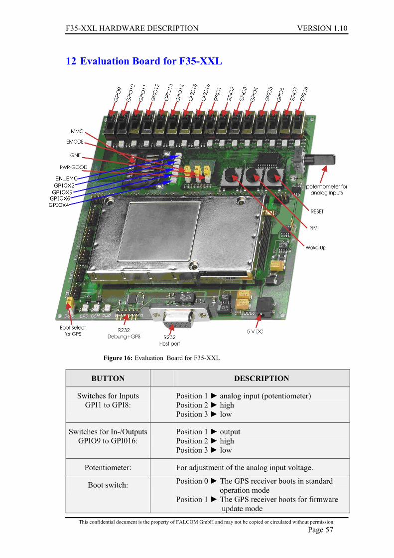
F35-XXL HARDWARE DESCRIPTION VERSION 1.10
This confidential document is the property of FALCOM GmbH and may not be copied or circulated without permission. Page 57
12 Evaluation Board for F35-XXL
Figure 16: Evaluation Board for F35-XXL
BUTTON DESCRIPTION
Switches for Inputs GPI1 to GPI8:
Position 1 analog input (potentiometer) Position 2 high Position 3 low
Switches for In-/Outputs GPIO9 to GPI016:
Position 1 output Position 2 high Position 3 low
Potentiometer: For adjustment of the analog input voltage.
Boot switch:
Position 0 The GPS receiver boots in standard operation mode Position 1 The GPS receiver boots for firmware update mode
F35-XXL HARDWARE DESCRIPTION VERSION 1.10
This confidential document is the property of FALCOM GmbH and may not be copied or circulated without permission. Page 58
EMODE switch:
Position 0 The V850 boots the RedBoot from the internal ROM Position 1 The V850 boots the RedBoot from the external FLASH
IGNIT switch: Position 0 The IGNITION line is set to high Position 1 The IGNITION line is set to low
USA switch: Position 0 The PWR_GOOD line is set to high Position 1 The PWR_GOOD line is set to low
WakeUp button Pulls the WakeUp signal to low
NMI button Polls the NMI signal to low
RESET Hardware reset table14: F35-XXL- EVAL- BOARD -Button specification.
The pin specification of the F35-XXL-EVAL- BOARD is shown in below Table.
Desig-nation PINS Address on the F35-XXL
Pin1 PLD_TCK
Pin2 Vcc
Pin3 PLD_TDO
Pin4 NONE
Pin5 PLD_TDI
Pin6 NONE
Pin7 PLD_TMS
JTA
G
Pin8 GND
Pin1 AD0
Pin2 AD1
Pin3 AD2
Pin4 AD3
Pin5 AD4
Pin6 AD5
Pin7 AD6
AD
0-7
Pin8 AD7
F35-XXL HARDWARE DESCRIPTION VERSION 1.10
This confidential document is the property of FALCOM GmbH and may not be copied or circulated without permission. Page 59
Pin1 DAT_MMC
Pin2 EN_SNT
Pin3 CMD_MMC
Pin4 EN_VCC
Pin5 CLK_MMC
Pin6 EN_HA
Pin7 CS_MMC
MM
C P
ower
Mg
Pin8 EN_MMC
Pin1 TXB
Pin2 CTSB
Pin3 RXB
Pin4 RIB
Pin5 DTRB
Pin6 DSRB
Pin7 RTSB
RS2
32 F
ull-
3V
Pin8 DCDB
Pin1 GPIO9
INPU
T/
OU
TP
UT
Pin2 GPIO10
Pin3 GPIO11
Pin4 GPIO12
Pin5 GPIO13
Pin6 GPIO14
Pin7 GPIO15 INPU
T/O
UT
PUT
Pin8 GPIO16
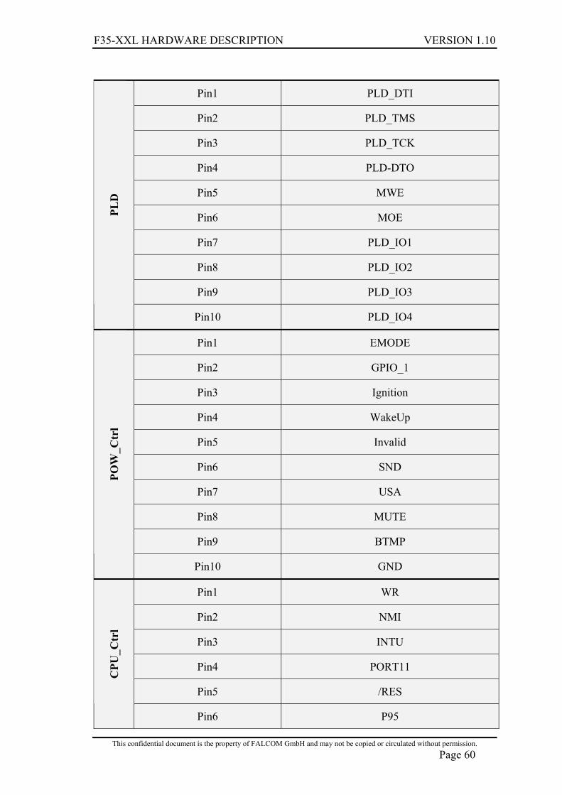
F35-XXL HARDWARE DESCRIPTION VERSION 1.10
This confidential document is the property of FALCOM GmbH and may not be copied or circulated without permission. Page 60
Pin1 PLD_DTI
Pin2 PLD_TMS
Pin3 PLD_TCK
Pin4 PLD-DTO
Pin5 MWE
Pin6 MOE
Pin7 PLD_IO1
Pin8 PLD_IO2
Pin9 PLD_IO3
PLD
Pin10 PLD_IO4
Pin1 EMODE
Pin2 GPIO_1
Pin3 Ignition
Pin4 WakeUp
Pin5 Invalid
Pin6 SND
Pin7 USA
Pin8 MUTE
Pin9 BTMP
POW
_Ctr
l
Pin10 GND
Pin1 WR
Pin2 NMI
Pin3 INTU
Pin4 PORT11
Pin5 /RES
CPU
_Ctr
l
Pin6 P95
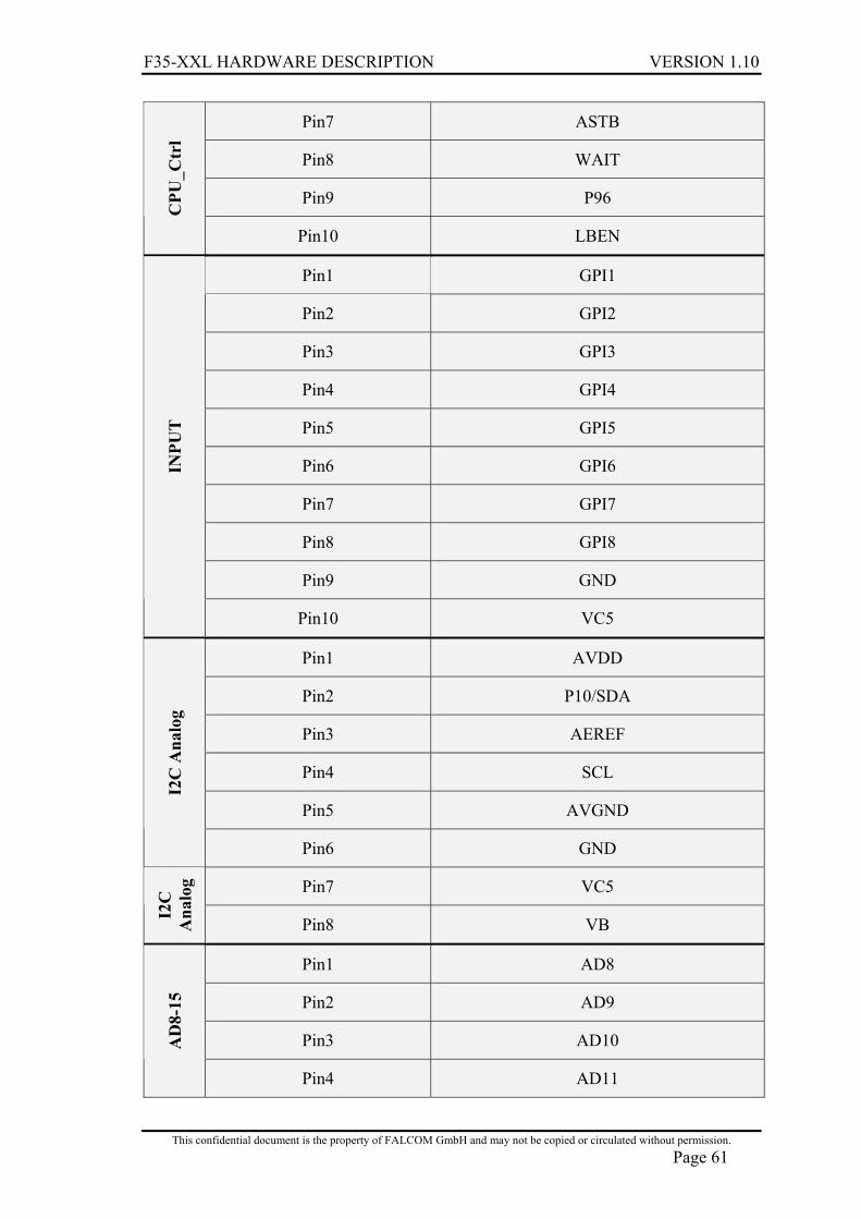
F35-XXL HARDWARE DESCRIPTION VERSION 1.10
This confidential document is the property of FALCOM GmbH and may not be copied or circulated without permission. Page 61
Pin7 ASTB
Pin8 WAIT
Pin9 P96 C
PU_C
trl
Pin10 LBEN
Pin1 GPI1
Pin2 GPI2
Pin3 GPI3
Pin4 GPI4
Pin5 GPI5
Pin6 GPI6
Pin7 GPI7
Pin8 GPI8
Pin9 GND
INPU
T
Pin10 VC5
Pin1 AVDD
Pin2 P10/SDA
Pin3 AEREF
Pin4 SCL
Pin5 AVGND
I2C
Ana
log
Pin6 GND
Pin7 VC5
I2C
A
nalo
g
Pin8 VB
Pin1 AD8
Pin2 AD9
Pin3 AD10 AD
8-15
Pin4 AD11
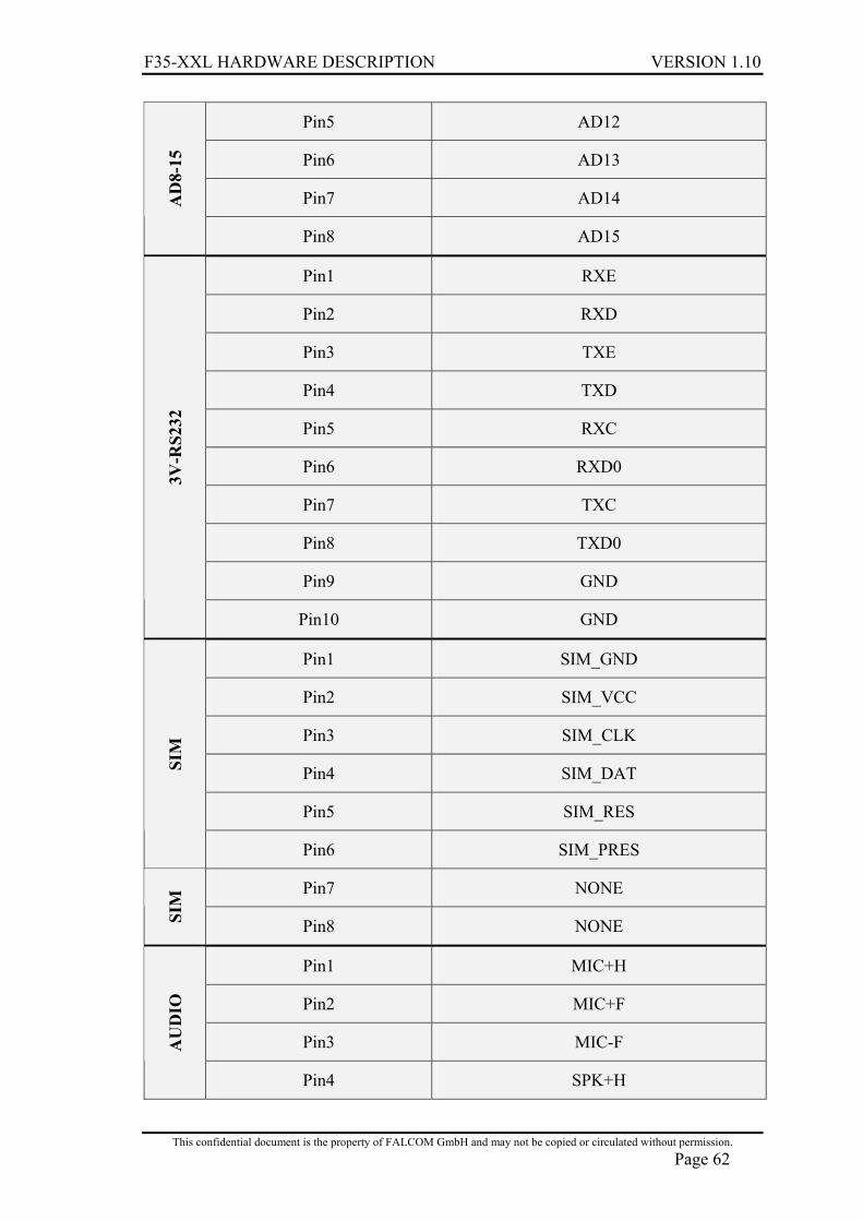
F35-XXL HARDWARE DESCRIPTION VERSION 1.10
This confidential document is the property of FALCOM GmbH and may not be copied or circulated without permission. Page 62
Pin5 AD12
Pin6 AD13
Pin7 AD14 AD
8-15
Pin8 AD15
Pin1 RXE
Pin2 RXD
Pin3 TXE
Pin4 TXD
Pin5 RXC
Pin6 RXD0
Pin7 TXC
Pin8 TXD0
Pin9 GND
3V-R
S232
Pin10 GND
Pin1 SIM_GND
Pin2 SIM_VCC
Pin3 SIM_CLK
Pin4 SIM_DAT
Pin5 SIM_RES
SIM
Pin6 SIM_PRES
Pin7 NONE
SIM
Pin8 NONE
Pin1 MIC+H
Pin2 MIC+F
Pin3 MIC-F AU
DIO
Pin4 SPK+H

F35-XXL HARDWARE DESCRIPTION VERSION 1.10
This confidential document is the property of FALCOM GmbH and may not be copied or circulated without permission. Page 63
Pin5 SPK+F
Pin6 SPK+F
Pin7 SPK-H AU
DIO
Pin8 SPK-F
Pin1 BootSel
Pin2 GPIOAG
Pin3 GPIO5G
Pin4 GPOX7 (it can be programmed e.g. as TMARK)
Pin5 GPIO6G
Pin6 GPIO10G
Pin7 GPIO7G
GPS
Pin8 GND
table14: F35-XXL- EVAL- BOARD -pin specification.
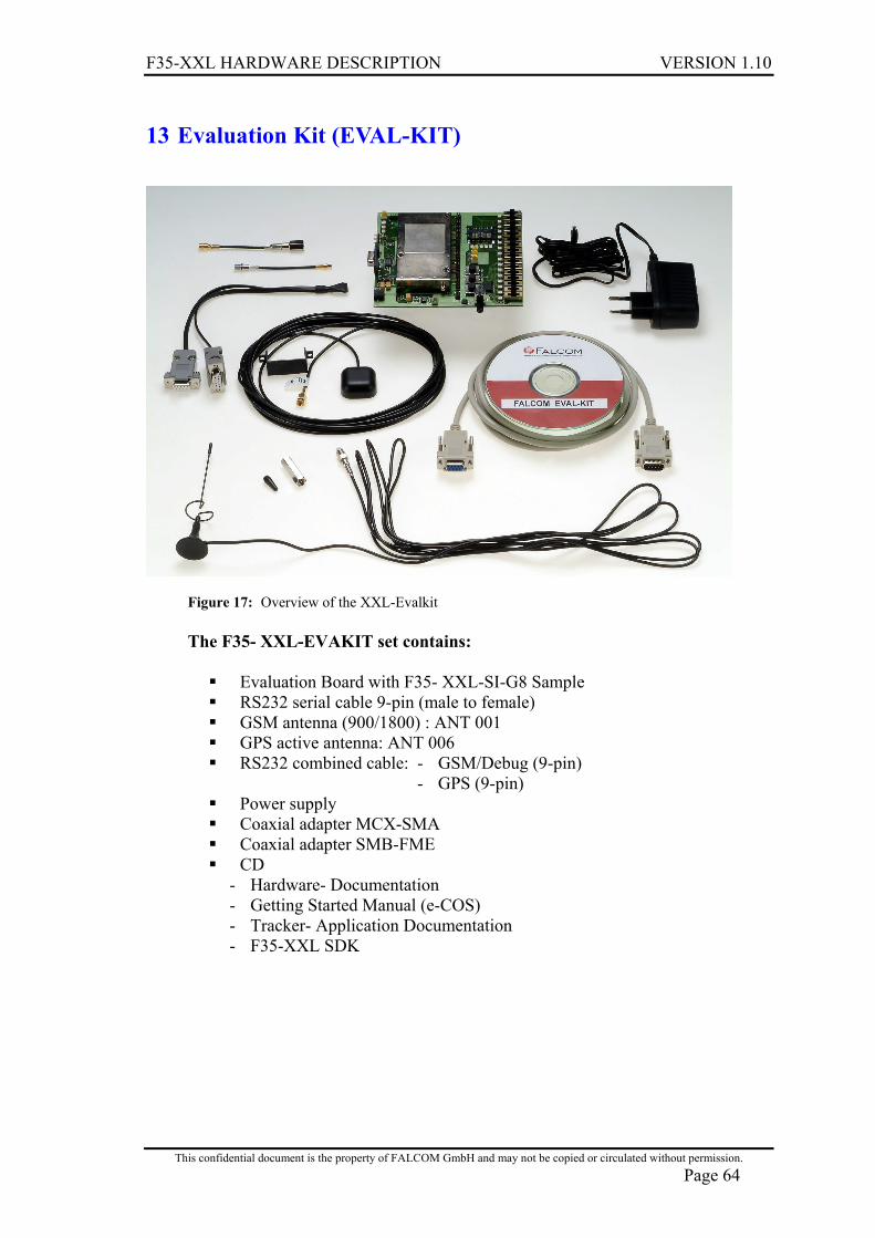
F35-XXL HARDWARE DESCRIPTION VERSION 1.10
This confidential document is the property of FALCOM GmbH and may not be copied or circulated without permission. Page 64
13 Evaluation Kit (EVAL-KIT)
Figure 17: Overview of the XXL-Evalkit The F35- XXL-EVAKIT set contains: Evaluation Board with F35- XXL-SI-G8 Sample RS232 serial cable 9-pin (male to female) GSM antenna (900/1800) : ANT 001 GPS active antenna: ANT 006 RS232 combined cable: - GSM/Debug (9-pin)
- GPS (9-pin) Power supply Coaxial adapter MCX-SMA Coaxial adapter SMB-FME CD
- Hardware- Documentation - Getting Started Manual (e-COS) - Tracker- Application Documentation - F35-XXL SDK
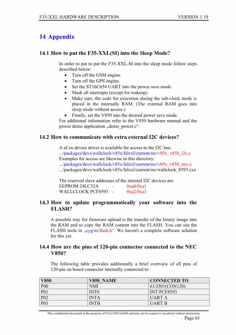
F35-XXL HARDWARE DESCRIPTION VERSION 1.10
This confidential document is the property of FALCOM GmbH and may not be copied or circulated without permission. Page 65
14 Appendix
14.1 How to put the F35-XXL(SI) into the Sleep Mode?
In order to put to put the F35-XXL-SI into the sleep mode follow steps described below:
• Turn off the GSM engine. • Turn off the GPS engine. • Set the ST16C654 UART into the power save mode • Mask all interrupts (except for wakeup) • Make sure, the code for execution during the sub-clock mode is
placed in the internally RAM. (The external RAM goes into sleep mode without access.)
• Finally, set the V850 into the desired power save mode. For additional information refer to the V850 hardware manual and the power demo application „demo_power.c“.
14.2 How to communicate with extra external I2C devices?
A eCos device driver is available for access to the I2C bus: .../packages/devs/wallclock/v85x/falxxl/current/src/v85x_v850_i2c.c Examples for access are likewise in this directory: .../packages/devs/wallclock/v85x/falxxl/current/src/v85x_v850_env.c .../packages/devs/wallclock/v85x/falxxl/current/src/wallclock_8593.cxx The reserved slave addresses of the internal I2C devices are: EEPROM 24LC32A - 0xa0/0xa1 WALLCLOCK PCF8593 - 0xa2/0xa3
14.3 How to update programmatically your software into the FLASH?
A possible way for firmware upload is the transfer of the binary image into the RAM and to copy the RAM content into the FLASH. You can use the FLASH tools in „cyg/io/flash.h“. We haven't a complete software solution for this yet.
14.4 How are the pins of 120-pin connector connected to the NEC V850?
The following table provides additionally a brief overview of all pins of 120-pin on board connector internally connected to:
V850 V850_NAME CONNECTED TO P00 NMI 61/J301(CON120) P01 INT0 INT PCF8593 P02 INTA UART A P03 INTB UART B
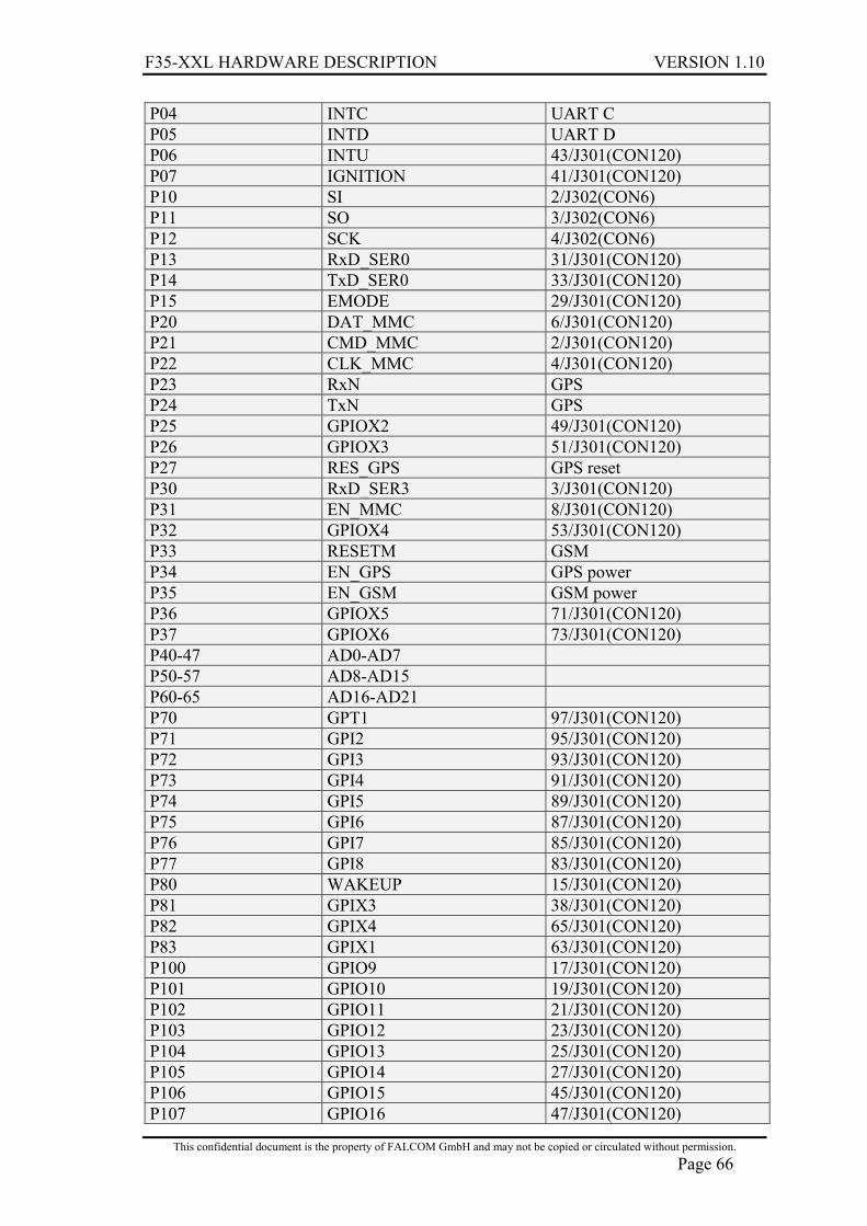
F35-XXL HARDWARE DESCRIPTION VERSION 1.10
This confidential document is the property of FALCOM GmbH and may not be copied or circulated without permission. Page 66
P04 INTC UART C P05 INTD UART D P06 INTU 43/J301(CON120) P07 IGNITION 41/J301(CON120) P10 SI 2/J302(CON6) P11 SO 3/J302(CON6) P12 SCK 4/J302(CON6) P13 RxD_SER0 31/J301(CON120) P14 TxD_SER0 33/J301(CON120) P15 EMODE 29/J301(CON120) P20 DAT_MMC 6/J301(CON120) P21 CMD_MMC 2/J301(CON120) P22 CLK_MMC 4/J301(CON120) P23 RxN GPS P24 TxN GPS P25 GPIOX2 49/J301(CON120) P26 GPIOX3 51/J301(CON120) P27 RES_GPS GPS reset P30 RxD_SER3 3/J301(CON120) P31 EN_MMC 8/J301(CON120) P32 GPIOX4 53/J301(CON120) P33 RESETM GSM P34 EN_GPS GPS power P35 EN_GSM GSM power P36 GPIOX5 71/J301(CON120) P37 GPIOX6 73/J301(CON120) P40-47 AD0-AD7 P50-57 AD8-AD15 P60-65 AD16-AD21 P70 GPT1 97/J301(CON120) P71 GPI2 95/J301(CON120) P72 GPI3 93/J301(CON120) P73 GPI4 91/J301(CON120) P74 GPI5 89/J301(CON120) P75 GPI6 87/J301(CON120) P76 GPI7 85/J301(CON120) P77 GPI8 83/J301(CON120) P80 WAKEUP 15/J301(CON120) P81 GPIX3 38/J301(CON120) P82 GPIX4 65/J301(CON120) P83 GPIX1 63/J301(CON120) P100 GPIO9 17/J301(CON120) P101 GPIO10 19/J301(CON120) P102 GPIO11 21/J301(CON120) P103 GPIO12 23/J301(CON120) P104 GPIO13 25/J301(CON120) P105 GPIO14 27/J301(CON120) P106 GPIO15 45/J301(CON120) P107 GPIO16 47/J301(CON120)
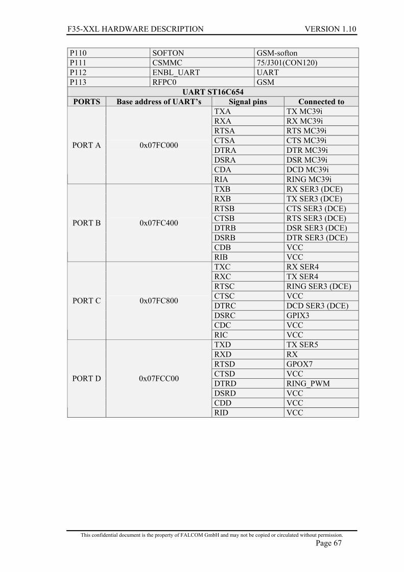
F35-XXL HARDWARE DESCRIPTION VERSION 1.10
This confidential document is the property of FALCOM GmbH and may not be copied or circulated without permission. Page 67
P110 SOFTON GSM-softon P111 CSMMC 75/J301(CON120) P112 ENBL_UART UART P113 RFPC0 GSM
UART ST16C654 PORTS Base address of UART’s Signal pins Connected to
TXA TX MC39i RXA RX MC39i RTSA RTS MC39i CTSA CTS MC39i DTRA DTR MC39i DSRA DSR MC39i CDA DCD MC39i
PORT A 0x07FC000
RIA RING MC39i TXB RX SER3 (DCE) RXB TX SER3 (DCE) RTSB CTS SER3 (DCE) CTSB RTS SER3 (DCE) DTRB DSR SER3 (DCE) DSRB DTR SER3 (DCE) CDB VCC
PORT B 0x07FC400
RIB VCC TXC RX SER4 RXC TX SER4 RTSC RING SER3 (DCE) CTSC VCC DTRC DCD SER3 (DCE) DSRC GPIX3 CDC VCC
PORT C 0x07FC800
RIC VCC TXD TX SER5 RXD RX RTSD GPOX7 CTSD VCC DTRD RING_PWM DSRD VCC CDD VCC
PORT D 0x07FCC00
RID VCC
F35-XXL HARDWARE DESCRIPTION VERSION 1.10
This confidential document is the property of FALCOM GmbH and may not be copied or circulated without permission. Page 68
14.5 EVAL-BOARD circuit diagram
F35-XXL HARDWARE DESCRIPTION VERSION 1.10
This confidential document is the property of FALCOM GmbH and may not be copied or circulated without permission. Page 69
F35-XXL HARDWARE DESCRIPTION VERSION 1.10
This confidential document is the property of FALCOM GmbH and may not be copied or circulated without permission. Page 70
14.6 EVAL-BOARD pin out


![f35-frosh-sem-3d-models-2d-images.ppt - UCSBparhami/pres_folder/f35...Microsoft PowerPoint - f35-frosh-sem-3d-models-2d-images.ppt [Compatibility Mode] Author: parha Created Date:](https://img.pdfslide.us/doc/110x75/6020bbfbc069bf413e212b45/f35-frosh-sem-3d-models-2d-ucsb-parhamipresfolderf35-microsoft-powerpoint.jpg)