Embed Size (px)
Citation preview
FINAL PROJECT REPORT
EE3390 ELECTRONIC CIRCUITS DESIGN LAB
POWER INVERTER
Craig Danton
Nimit Mehta
Submitted in partial fulfillment of the requirements for the
Bachelor’s of Science Degree
December 11
th, 2008
Department of Electrical Engineering
Columbia University
TABLE OF CONTENTS I. EXECUTIVE SUMMARY II. BLOCK DIAGRAM, DESIGN TARGETS AND SPECIFICATIONS
III. INDIVIDUAL BLOCK DESCRIPTIONS
IV. BILL OF MATERIALS V. HEALTH, SAFETY, & ENVIRONMENTAL ISSUES
VI. FINAL GANTT CHART
VII. CRITICISM OF THIS COURSE
APPENDICES
VIII. WAVEFORM OUTPUTS
IX. OSCILLATOR RESOURCES: TI-BUBBA OSCILLATOR
I. EXECUTIVE SUMMARY
With the push in the past ten years to improve methods of energy generation, there has been an increasing
need to optimize energy management. Our project was to create a DC to AC load-balanced inverter. The
function would be to take in a DC voltage input, something like a battery or a solar cell, and output an AC voltage, resembling that which comes out of a wall outlet. The crux of the design would be that it would
be “load balanced” meaning that no matter how large of a load (which could resemble anything from an
array of lightbulbs to a laptop) the output voltage would not change.
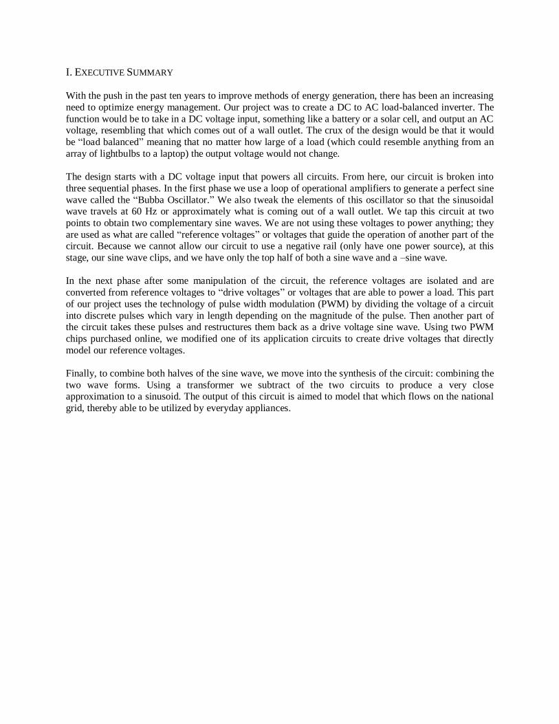
The design starts with a DC voltage input that powers all circuits. From here, our circuit is broken into
three sequential phases. In the first phase we use a loop of operational amplifiers to generate a perfect sine
wave called the “Bubba Oscillator.” We also tweak the elements of this oscillator so that the sinusoidal wave travels at 60 Hz or approximately what is coming out of a wall outlet. We tap this circuit at two
points to obtain two complementary sine waves. We are not using these voltages to power anything; they
are used as what are called “reference voltages” or voltages that guide the operation of another part of the circuit. Because we cannot allow our circuit to use a negative rail (only have one power source), at this
stage, our sine wave clips, and we have only the top half of both a sine wave and a –sine wave.
In the next phase after some manipulation of the circuit, the reference voltages are isolated and are
converted from reference voltages to “drive voltages” or voltages that are able to power a load. This part
of our project uses the technology of pulse width modulation (PWM) by dividing the voltage of a circuit
into discrete pulses which vary in length depending on the magnitude of the pulse. Then another part of the circuit takes these pulses and restructures them back as a drive voltage sine wave. Using two PWM
chips purchased online, we modified one of its application circuits to create drive voltages that directly
model our reference voltages.
Finally, to combine both halves of the sine wave, we move into the synthesis of the circuit: combining the
two wave forms. Using a transformer we subtract of the two circuits to produce a very close approximation to a sinusoid. The output of this circuit is aimed to model that which flows on the national
grid, thereby able to be utilized by everyday appliances.
II. BLOCK DIAGRAM
III. DIAGRAM EXPLANATION
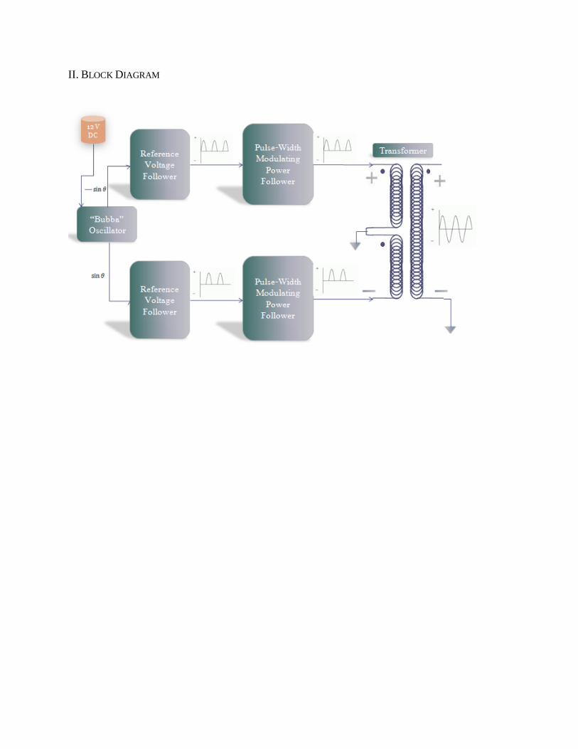
A. OP-AMP SINE WAVE “BUBBA” OSCILLATOR BLOCK The first step in building a precision sine wave inverter is to build a reference sine wave that can then be
used in a power voltage follower to produce the desired output, however producing a circuit that oscillates
accurately at 60 Hz can be challenging. Preferably, in addition we needed the circuit to produce a -sine wave, or negative rectify our sine wave to produce the input of our other voltage follower which would
then be set up to be the negative half of the output sine wave.
Fig. 1 Bubba Oscillator Block Diagram
Design Process We initially began with the idea that making an oscillator that operated at a higher frequency (a multiple
of 60Hz), to avoid having large capacitive circuit components. This signal would then be put through j/k
flip flops to reduce the frequency by half every step until we got a 60Hz square wave. In theory this circuit could then be put into a low-pass filter to filter out the lower frequencies of the Fourier Series. This
would in summation turn the square wave into a sine wave and finally it would be rectified to produce the
necessary -sine wave components as well.
When we implemented this concept first, we were able to create the oscillator however, neither the digital
counter logic, nor the sequential J/K flip flop arrangement was responding to input signal we gave it in
any consistent manner. Finally we realized that making an inverting rectifier would also require a negative voltage rail, which is not present in the input of an inverter. We decided to approach the problem
from a different perspective, and researched low frequency oscillator circuits that only use a positive rail
and our solution was the so-called “bubba” oscillator
Final Design
A Bubba oscillator is an op-amp sine wave oscillator circuit, that relies on the principle of setting a circuit
into an unstable oscillation using passive circuit components. In general to produce a lasting oscillation we need their to unity gain through the entire loop of op-amps. A gain of greater than one and the output
will look more like a square wave and a gain of the less than one and the circuit will eventually stop
oscillating. The second requirement is that we produce a 180 degree phase shift throughout the entire circuit and considering that we can achieve a maximum of 90 degrees per pole we will need at least two
poles in the entire circuit. In theory then a sine wave oscillator can be made from one op-amp with two
poles in its feedback however this makes the circuit extremely sensitive to changes in phase.
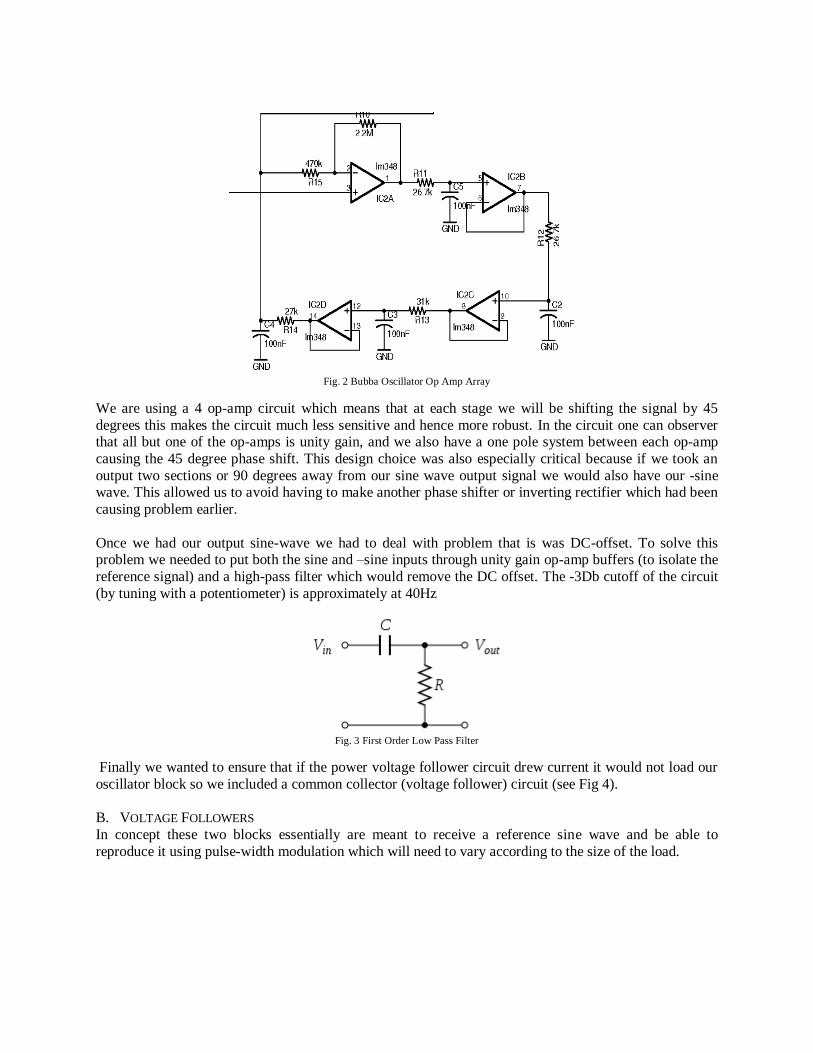
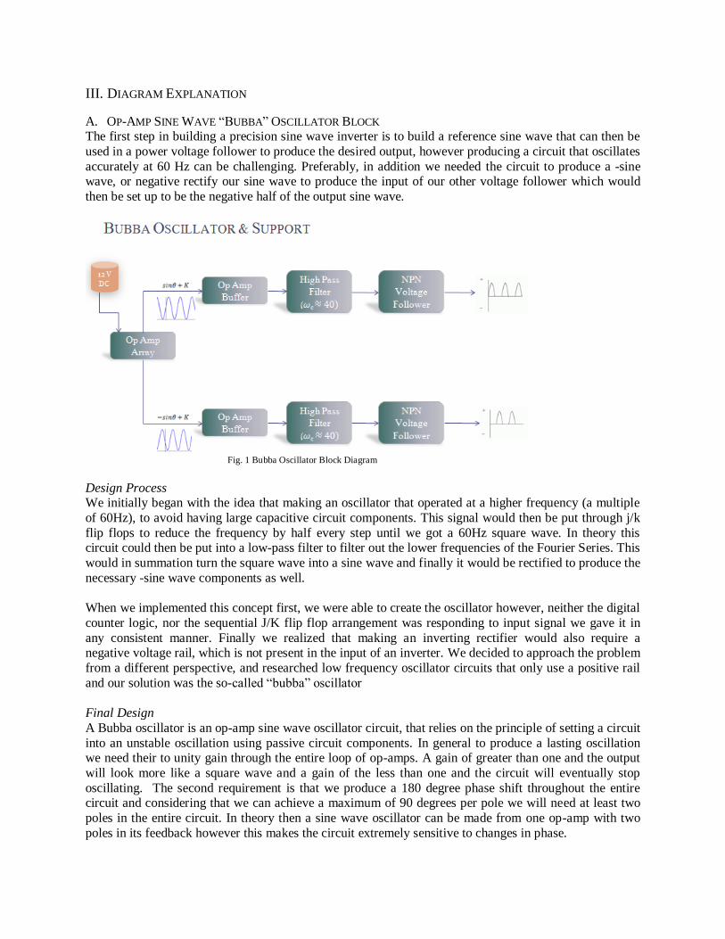
Fig. 2 Bubba Oscillator Op Amp Array
We are using a 4 op-amp circuit which means that at each stage we will be shifting the signal by 45
degrees this makes the circuit much less sensitive and hence more robust. In the circuit one can observer that all but one of the op-amps is unity gain, and we also have a one pole system between each op-amp
causing the 45 degree phase shift. This design choice was also especially critical because if we took an
output two sections or 90 degrees away from our sine wave output signal we would also have our -sine wave. This allowed us to avoid having to make another phase shifter or inverting rectifier which had been
causing problem earlier.
Once we had our output sine-wave we had to deal with problem that is was DC-offset. To solve this problem we needed to put both the sine and –sine inputs through unity gain op-amp buffers (to isolate the
reference signal) and a high-pass filter which would remove the DC offset. The -3Db cutoff of the circuit
(by tuning with a potentiometer) is approximately at 40Hz
Fig. 3 First Order Low Pass Filter
Finally we wanted to ensure that if the power voltage follower circuit drew current it would not load our
oscillator block so we included a common collector (voltage follower) circuit (see Fig 4).
B. VOLTAGE FOLLOWERS
In concept these two blocks essentially are meant to receive a reference sine wave and be able to
reproduce it using pulse-width modulation which will need to vary according to the size of the load.
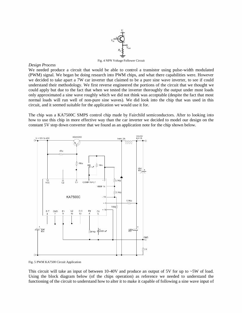
Fig. 4 NPN Voltage Follower Circuit
Design Process We needed produce a circuit that would be able to control a transistor using pulse-width modulated
(PWM) signal. We began be doing research into PWM chips, and what there capabilities were. However
we decided to take apart a 7W car inverter that claimed to be a pure sine wave inverter, to see if could
understand their methodology. We first reverse engineered the portions of the circuit that we thought we could apply but due to the fact that when we tested the inverter thoroughly the output under most loads
only approximated a sine wave roughly which we did not think was acceptable (despite the fact that most
normal loads will run well of non-pure sine waves). We did look into the chip that was used in this circuit, and it seemed suitable for the application we would use it for.
The chip was a KA7500C SMPS control chip made by Fairchild semiconductors. After to looking into how to use this chip in more effective way than the car inverter we decided to model our design on the
constant 5V step down converter that we found as an application note for the chip shown below.
Fig. 5 PWM KA7500 Circuit Application
This circuit will take an input of between 10-40V and produce an output of 5V for up to ~5W of load.
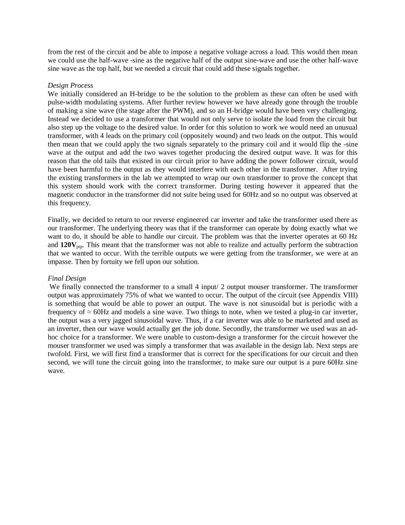
Using the block diagram below (of the chips operation) as reference we needed to understand the functioning of the circuit to understand how to alter it to make it capable of following a sine wave input of
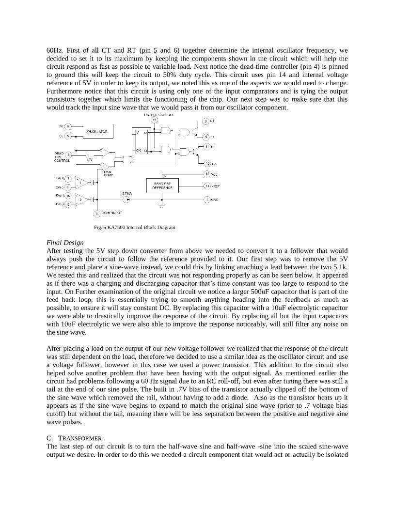
60Hz. First of all CT and RT (pin 5 and 6) together determine the internal oscillator frequency, we
decided to set it to its maximum by keeping the components shown in the circuit which will help the circuit respond as fast as possible to variable load. Next notice the dead-time controller (pin 4) is pinned
to ground this will keep the circuit to 50% duty cycle. This circuit uses pin 14 and internal voltage
reference of 5V in order to keep its output, we noted this as one of the aspects we would need to change.
Furthermore notice that this circuit is using only one of the input comparators and is tying the output transistors together which limits the functioning of the chip. Our next step was to make sure that this
would track the input sine wave that we would pass it from our oscillator component.
Fig. 6 KA7500 Internal Block Diagram
Final Design
After testing the 5V step down converter from above we needed to convert it to a follower that would
always push the circuit to follow the reference provided to it. Our first step was to remove the 5V reference and place a sine-wave instead, we could this by linking attaching a lead between the two 5.1k.
We tested this and realized that the circuit was not responding properly as can be seen below. It appeared
as if there was a charging and discharging capacitor that’s time constant was too large to respond to the
input. On Further examination of the original circuit we notice a larger 500uF capacitor that is part of the feed back loop, this is essentially trying to smooth anything heading into the feedback as much as
possible, to ensure it will stay constant DC. By replacing this capacitor with a 10uF electrolytic capacitor
we were able to drastically improve the response of the circuit. By replacing all but the input capacitors with 10uF electrolytic we were also able to improve the response noticeably, will still filter any noise on
the sine wave.
After placing a load on the output of our new voltage follower we realized that the response of the circuit
was still dependent on the load, therefore we decided to use a similar idea as the oscillator circuit and use
a voltage follower, however in this case we used a power transistor. This addition to the circuit also
helped solve another problem that have been having with the output signal. As mentioned earlier the circuit had problems following a 60 Hz signal due to an RC roll-off, but even after tuning there was still a
tail at the end of our sine pulse. The built in .7V bias of the transistor actually clipped off the bottom of
the sine wave which removed the tail, without having to add a diode. Also as the transistor heats up it appears as if the sine wave begins to expand to match the original sine wave (prior to .7 voltage bias
cutoff) but without the tail, meaning there will be less separation between the positive and negative sine
wave pulses.
C. TRANSFORMER
The last step of our circuit is to turn the half-wave sine and half-wave -sine into the scaled sine-wave
output we desire. In order to do this we needed a circuit component that would act or actually be isolated
from the rest of the circuit and be able to impose a negative voltage across a load. This would then mean
we could use the half-wave -sine as the negative half of the output sine-wave and use the other half-wave sine wave as the top half, but we needed a circuit that could add these signals together.
Design Process
We initially considered an H-bridge to be the solution to the problem as these can often be used with pulse-width modulating systems. After further review however we have already gone through the trouble
of making a sine wave (the stage after the PWM), and so an H-bridge would have been very challenging.
Instead we decided to use a transformer that would not only serve to isolate the load from the circuit but also step up the voltage to the desired value. In order for this solution to work we would need an unusual
transformer, with 4 leads on the primary coil (oppositely wound) and two leads on the output. This would
then mean that we could apply the two signals separately to the primary coil and it would flip the -sine wave at the output and add the two waves together producing the desired output wave. It was for this
reason that the old tails that existed in our circuit prior to have adding the power follower circuit, would
have been harmful to the output as they would interfere with each other in the transformer. After trying
the existing transformers in the lab we attempted to wrap our own transformer to prove the concept that this system should work with the correct transformer. During testing however it appeared that the
magnetic conductor in the transformer did not suite being used for 60Hz and so no output was observed at
this frequency.
Finally, we decided to return to our reverse engineered car inverter and take the transformer used there as
our transformer. The underlying theory was that if the transformer can operate by doing exactly what we want to do, it should be able to handle our circuit. The problem was that the inverter operates at 60 Hz
and 120Vptp. This meant that the transformer was not able to realize and actually perform the subtraction
that we wanted to occur. With the terrible outputs we were getting from the transformer, we were at an
impasse. Then by fortuity we fell upon our solution.
Final Design
We finally connected the transformer to a small 4 input/ 2 output mouser transformer. The transformer output was approximately 75% of what we wanted to occur. The output of the circuit (see Appendix VIII)
is something that would be able to power an output. The wave is not sinusoidal but is periodic with a
frequency of ≈ 60Hz and models a sine wave. Two things to note, when we tested a plug-in car inverter,
the output was a very jagged sinusoidal wave. Thus, if a car inverter was able to be marketed and used as an inverter, then our wave would actually get the job done. Secondly, the transformer we used was an ad-
hoc choice for a transformer. We were unable to custom-design a transformer for the circuit however the
mouser transformer we used was simply a transformer that was available in the design lab. Next steps are twofold. First, we will first find a transformer that is correct for the specifications for our circuit and then
second, we will tune the circuit going into the transformer, to make sure our output is a pure 60Hz sine
wave.
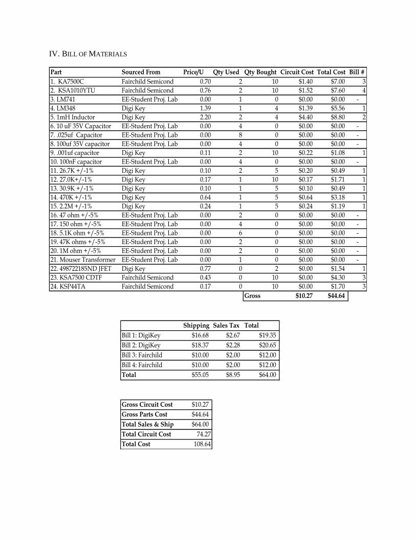
IV. BILL OF MATERIALS
Part Sourced From Price/U Qty Used Qty Bought Circuit Cost Total Cost Bill #
1. KA7500C Fairchild Semicond 0.70 2 10 $1.40 $7.00 3
2. KSA1010YTU Fairchild Semicond 0.76 2 10 $1.52 $7.60 4
3. LM741 EE-Student Proj. Lab 0.00 1 0 $0.00 $0.00 -
4. LM348 Digi Key 1.39 1 4 $1.39 $5.56 1
5. 1mH Inductor Digi Key 2.20 2 4 $4.40 $8.80 2
6. 10 uF 35V Capacitor EE-Student Proj. Lab 0.00 4 0 $0.00 $0.00 -
7. .025uf Capacitor EE-Student Proj. Lab 0.00 8 0 $0.00 $0.00 -
8. 100uf 35V capacitor EE-Student Proj. Lab 0.00 4 0 $0.00 $0.00 -
9. .001uf capacitor Digi Key 0.11 2 10 $0.22 $1.08 1
10. 100nF capacitor EE-Student Proj. Lab 0.00 4 0 $0.00 $0.00 -
11. 26.7K +/-1% Digi Key 0.10 2 5 $0.20 $0.49 1
12. 27.0K+/-1% Digi Key 0.17 1 10 $0.17 $1.71 1
13. 30.9K +/-1% Digi Key 0.10 1 5 $0.10 $0.49 1
14. 470K +/-1% Digi Key 0.64 1 5 $0.64 $3.18 1
15. 2.2M +/-1% Digi Key 0.24 1 5 $0.24 $1.19 1
16. 47 ohm +/-5% EE-Student Proj. Lab 0.00 2 0 $0.00 $0.00 -
17. 150 ohm +/-5% EE-Student Proj. Lab 0.00 4 0 $0.00 $0.00 -
18. 5.1K ohm +/-5% EE-Student Proj. Lab 0.00 6 0 $0.00 $0.00 -
19. 47K ohms +/-5% EE-Student Proj. Lab 0.00 2 0 $0.00 $0.00 -
20. 1M ohm +/-5% EE-Student Proj. Lab 0.00 2 0 $0.00 $0.00 -
21. Mouser Transformer EE-Student Proj. Lab 0.00 1 0 $0.00 $0.00 -
22. 498722185ND JFET Digi Key 0.77 0 2 $0.00 $1.54 1
23. KSA7500 CDTF Fairchild Semicond 0.43 0 10 $0.00 $4.30 3
24. KSP44TA Fairchild Semicond 0.17 0 10 $0.00 $1.70 3
Gross $10.27 $44.64
Shipping Sales Tax Total
Bill 1: DigiKey $16.68 $2.67 $19.35
Bill 2: DigiKey $18.37 $2.28 $20.65
Bill 3: Fairchild $10.00 $2.00 $12.00
Bill 4: Fairchild $10.00 $2.00 $12.00
Total $55.05 $8.95 $64.00
Gross Circuit Cost $10.27
Gross Parts Cost $44.64
Total Sales & Ship $64.00
Total Circuit Cost 74.27
Total Cost 108.64

V. HEALTH, SAFETY, & ENVIRONMENTAL ISSUES
There are only a few problems and risks associated with our project. When working with power however,
one has to constantly look for areas of overheating and electrical shock. Multiple transistors on the board,
namely the voltage followers get very hot during times of operations (around 200° C) and the pulse width modulating chip, though still operating within its required bounds, heats up as well. The non linear
objects in the circuit are cause for concern if heat is not accounted for.
The project meets all FCC standards and has not many issues with health. However, in terms of safety,
heat sinks are most crucial for the circuit to not cause adverse problems.
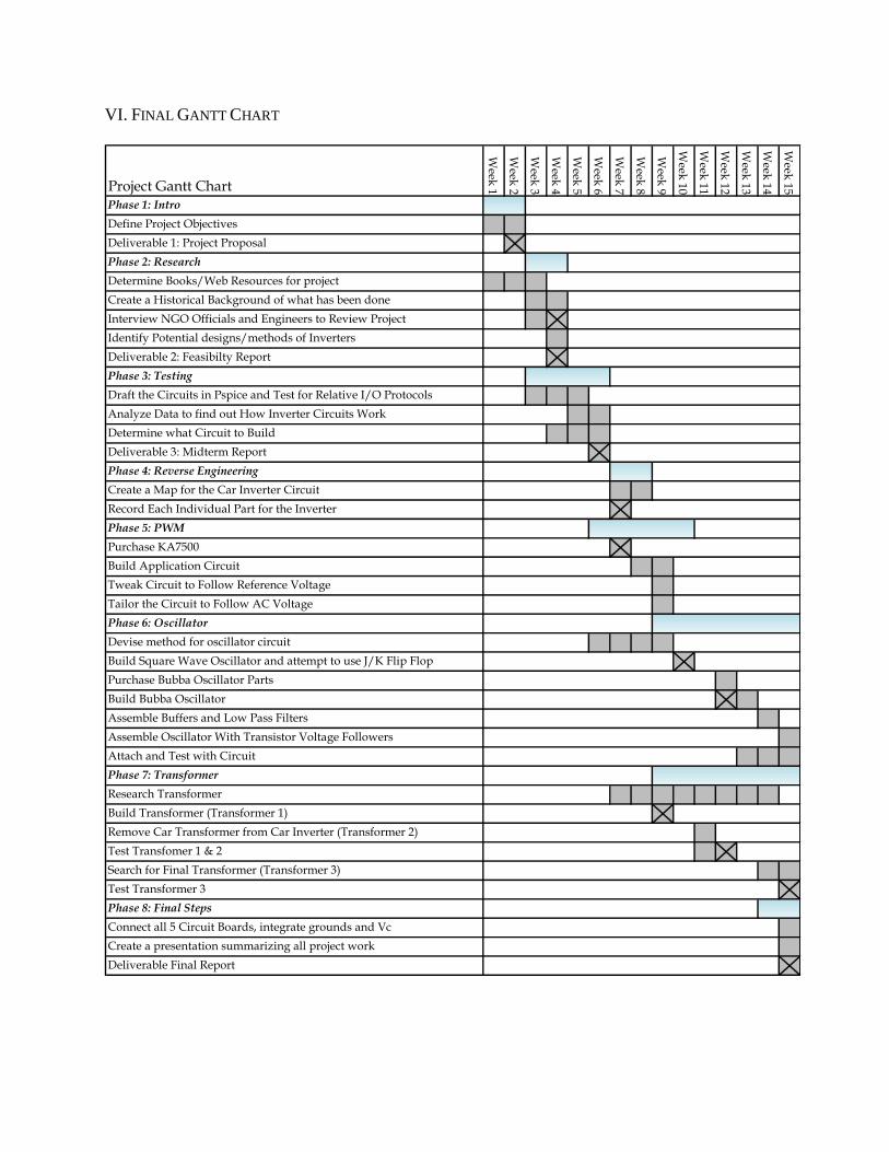
VI. FINAL GANTT CHART
Project Gantt Chart
Week
1
Week
2
Week
3
Week
4
Week
5
Week
6
Week
7
Week
8
Week
9
Week
10
Week
11
Week
12
Week
13
Week
14
Week
15
Phase 1: Intro
Define Project Objectives
Deliverable 1: Project Proposal
Phase 2: Research
Determine Books/Web Resources for project
Create a Historical Background of what has been done
Interview NGO Officials and Engineers to Review Project
Identify Potential designs/methods of Inverters
Deliverable 2: Feasibilty Report
Phase 3: Testing
Draft the Circuits in Pspice and Test for Relative I/O Protocols
Analyze Data to find out How Inverter Circuits Work
Determine what Circuit to Build
Deliverable 3: Midterm Report
Phase 4: Reverse Engineering
Create a Map for the Car Inverter Circuit
Record Each Individual Part for the Inverter
Phase 5: PWM
Purchase KA7500
Build Application Circuit
Tweak Circuit to Follow Reference Voltage
Tailor the Circuit to Follow AC Voltage
Phase 6: Oscillator
Devise method for oscillator circuit
Build Square Wave Oscillator and attempt to use J/K Flip Flop
Purchase Bubba Oscillator Parts
Build Bubba Oscillator
Assemble Buffers and Low Pass Filters
Assemble Oscillator With Transistor Voltage Followers
Attach and Test with Circuit
Phase 7: Transformer
Research Transformer
Build Transformer (Transformer 1)
Remove Car Transformer from Car Inverter (Transformer 2)
Test Transfomer 1 & 2
Search for Final Transformer (Transformer 3)
Test Transformer 3
Phase 8: Final Steps
Connect all 5 Circuit Boards, integrate grounds and Vc
Create a presentation summarizing all project work
Deliverable Final Report
VII. COURSE CRITICISM
Overall though it was more difficult and more vague in guidance, we liked how the course carried itself
out. We were given the chance to view many parts of the engineering design process and, unlike the first time around in Gateway, we were able to do it justice through using all of the electronic and design
techniques we have learned throughout the past three years.
Only a few suggestions for the course:
1. The student projects lab is a very poor location to have design projects stationed. I don’t know if
there is any way to monitor cleanliness in labs but coupled with the cramped space there is hardly
any place to work there. Secondly, the equipment is poor, wires and resources are scarce, and
there is only one viable choice for an oscilloscope. It is hard to believe that as seniors, we are
using much worse off equipment than sophomores and juniors use in their labs. There were many
options for circuit parts in terms of capacitors, inductors, resistors etc. but the rest of the lab was
lacking in almost everything.
2. Realistic goals are also so difficult to make early in a semester in terms of anticipating how
quickly a project will finish. We are very close to finishing the work that we set out to do but our
transformer is not working and therefore our project is in the twilight stages but still incomplete.
The thing is that early on in the semester we had no real idea that we needed a transformer. There
is a large time-inconsistency that comes into play when forecasting a timeline and though we
tried our best to meet the standards set, we weren’t able to. We think there must be a way to be
graded to take this into account.
We both loved the helpfulness of all three of the support staff and really could not have finished the project without your guidance.
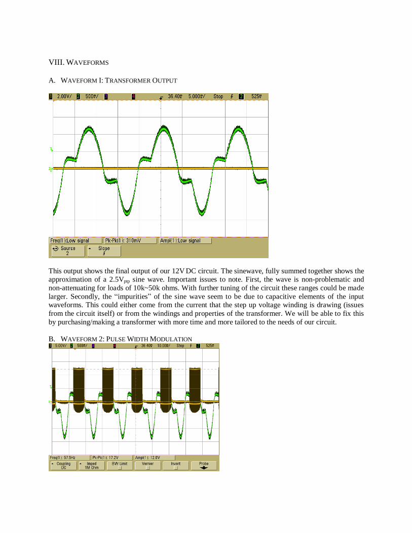
VIII. WAVEFORMS
A. WAVEFORM I: TRANSFORMER OUTPUT
This output shows the final output of our 12V DC circuit. The sinewave, fully summed together shows the approximation of a 2.5Vptp sine wave. Important issues to note. First, the wave is non-problematic and
non-attenuating for loads of 10k~50k ohms. With further tuning of the circuit these ranges could be made
larger. Secondly, the “impurities” of the sine wave seem to be due to capacitive elements of the input waveforms. This could either come from the current that the step up voltage winding is drawing (issues
from the circuit itself) or from the windings and properties of the transformer. We will be able to fix this
by purchasing/making a transformer with more time and more tailored to the needs of our circuit.
B. WAVEFORM 2: PULSE WIDTH MODULATION

This waveform shows the pulses made for the pulse width modulation of the circuit. The amount of
samples taken is so large that when the circuit is positive, there are many pulses and from a view of zoomed output, the pulses look like one black rectangle, though this is not actually the case.

IX. TI- SINE WAVE OSCILLATOR ARTICLE: “BUBBA OSCILLATOR”
Application ReportSLOA060 - March 2001
1
Sine-Wave OscillatorRon Mancini and Richard Palmer HPL (Dallas)
ABSTRACT
This note describes the operational amplifier (op-amp) sine-wave oscillator, together with thecriteria for oscillation to occur using RC components. It delineates the roles of phase shift andgain in the circuit and then discusses considerations of the op amp. A brief analysis of aWien-Bridge oscillator circuit is provided. Several examples of sine-wave oscillators aregiven, although it is recognized that there exist many additional types of oscillator to whichthe principles of this application note also apply.
Contents
1 Introduction 3. . . . . . . . . . . . . . . . . . . . . . . . . . . . . . . . . . . . . . . . . . . . . . . . . . . . . . . . . . . . . . . . . . . . . . . . .
2 Sine-Wave Oscillator Defined 3. . . . . . . . . . . . . . . . . . . . . . . . . . . . . . . . . . . . . . . . . . . . . . . . . . . . . . . . .
3 Requirements for Oscillation 3. . . . . . . . . . . . . . . . . . . . . . . . . . . . . . . . . . . . . . . . . . . . . . . . . . . . . . . . .
4 Phase Shift in the Oscillator 5. . . . . . . . . . . . . . . . . . . . . . . . . . . . . . . . . . . . . . . . . . . . . . . . . . . . . . . . . .
5 Gain in the Oscillator 6. . . . . . . . . . . . . . . . . . . . . . . . . . . . . . . . . . . . . . . . . . . . . . . . . . . . . . . . . . . . . . . .
6 Effect of the Active Element (Op Amp) on the Oscillator 7. . . . . . . . . . . . . . . . . . . . . . . . . . . . . . . .
7 Analysis of Oscillator Operation (Circuit) 8. . . . . . . . . . . . . . . . . . . . . . . . . . . . . . . . . . . . . . . . . . . . . .
8 Sine-Wave Oscillator Circuits 10. . . . . . . . . . . . . . . . . . . . . . . . . . . . . . . . . . . . . . . . . . . . . . . . . . . . . . . . 8.1 Wein-Bridge Oscillator 10. . . . . . . . . . . . . . . . . . . . . . . . . . . . . . . . . . . . . . . . . . . . . . . . . . . . . . . . . . . 8.2 Phase-Shift Oscillator, Single Amplifier 14. . . . . . . . . . . . . . . . . . . . . . . . . . . . . . . . . . . . . . . . . . . . . 8.3 Phase-Shift Oscillator, Buffered 16. . . . . . . . . . . . . . . . . . . . . . . . . . . . . . . . . . . . . . . . . . . . . . . . . . . . 8.4 Bubba Oscillator 17. . . . . . . . . . . . . . . . . . . . . . . . . . . . . . . . . . . . . . . . . . . . . . . . . . . . . . . . . . . . . . . . . 8.5 Quadrature Oscillator 18. . . . . . . . . . . . . . . . . . . . . . . . . . . . . . . . . . . . . . . . . . . . . . . . . . . . . . . . . . . .
9 Conclusion 19. . . . . . . . . . . . . . . . . . . . . . . . . . . . . . . . . . . . . . . . . . . . . . . . . . . . . . . . . . . . . . . . . . . . . . . . .
10 References 20. . . . . . . . . . . . . . . . . . . . . . . . . . . . . . . . . . . . . . . . . . . . . . . . . . . . . . . . . . . . . . . . . . . . . . . . .
List of Figures
1 Canonical Form of a System With Positive or Negative Feedback 4. . . . . . . . . . . . . . . . . . . . . . . . . . . . . 2 Phase Plot of RC Sections 5. . . . . . . . . . . . . . . . . . . . . . . . . . . . . . . . . . . . . . . . . . . . . . . . . . . . . . . . . . . . . . . 3 Op-Amp Frequency Response 7. . . . . . . . . . . . . . . . . . . . . . . . . . . . . . . . . . . . . . . . . . . . . . . . . . . . . . . . . . . . 4 Distortion vs Oscillation Frequency for Various Op-Amp Bandwidths 8. . . . . . . . . . . . . . . . . . . . . . . . . . . 5 Block Diagram of an Oscillator 9. . . . . . . . . . . . . . . . . . . . . . . . . . . . . . . . . . . . . . . . . . . . . . . . . . . . . . . . . . . . 6 Amplifier With Positive and Negative Feedback 9. . . . . . . . . . . . . . . . . . . . . . . . . . . . . . . . . . . . . . . . . . . . . 7 Wein-Bridge Circuit Schematic 10. . . . . . . . . . . . . . . . . . . . . . . . . . . . . . . . . . . . . . . . . . . . . . . . . . . . . . . . . . .
Trademarks are the property of their respective owners.

SLOA060
2 Sine-Wave Oscillator
8 Final Wein-Bridge Oscillator Circuit 11. . . . . . . . . . . . . . . . . . . . . . . . . . . . . . . . . . . . . . . . . . . . . . . . . . . . . . . 9 Wein-Bridge Output Waveforms: Effects of RF on Distortion 12. . . . . . . . . . . . . . . . . . . . . . . . . . . . . . . . . 10 Wein-Bridge Oscillator With Nonlinear Feedback 12. . . . . . . . . . . . . . . . . . . . . . . . . . . . . . . . . . . . . . . . . . 11 Output of the CIrcuit in Figure 10 13. . . . . . . . . . . . . . . . . . . . . . . . . . . . . . . . . . . . . . . . . . . . . . . . . . . . . . . . 12 Wein-Bridge Oscillator With AGC 14. . . . . . . . . . . . . . . . . . . . . . . . . . . . . . . . . . . . . . . . . . . . . . . . . . . . . . . 13 Output of the Circuit in Figure 12 14. . . . . . . . . . . . . . . . . . . . . . . . . . . . . . . . . . . . . . . . . . . . . . . . . . . . . . . . 14 Phase-Shift Oscillator (Single Op Amp) 15. . . . . . . . . . . . . . . . . . . . . . . . . . . . . . . . . . . . . . . . . . . . . . . . . . 15 Output of the Circuit in Figure 14 15. . . . . . . . . . . . . . . . . . . . . . . . . . . . . . . . . . . . . . . . . . . . . . . . . . . . . . . . 16 Phase-Shift Oscillator, Buffered 16. . . . . . . . . . . . . . . . . . . . . . . . . . . . . . . . . . . . . . . . . . . . . . . . . . . . . . . . . 17 Output of the Circuit Figure 16 16. . . . . . . . . . . . . . . . . . . . . . . . . . . . . . . . . . . . . . . . . . . . . . . . . . . . . . . . . . 18 Bubba Oscillator 17. . . . . . . . . . . . . . . . . . . . . . . . . . . . . . . . . . . . . . . . . . . . . . . . . . . . . . . . . . . . . . . . . . . . . . 19 Output of the Circuit in Figure 18 18. . . . . . . . . . . . . . . . . . . . . . . . . . . . . . . . . . . . . . . . . . . . . . . . . . . . . . . . 20 Quadrature Oscillator 19. . . . . . . . . . . . . . . . . . . . . . . . . . . . . . . . . . . . . . . . . . . . . . . . . . . . . . . . . . . . . . . . . . 21 Output of the Circuit in Figure 20 19. . . . . . . . . . . . . . . . . . . . . . . . . . . . . . . . . . . . . . . . . . . . . . . . . . . . . . . .
SLOA060
3 Sine-Wave Oscillator
1 IntroductionOscillators are circuits that produce specific, periodic waveforms such as square, triangular,sawtooth, and sinusoidal. They generally use some form of active device, lamp, or crystal,surrounded by passive devices such as resistors, capacitors, and inductors, to generate theoutput.
There are two main classes of oscillator: relaxation and sinusoidal. Relaxation oscillatorsgenerate the triangular, sawtooth and other nonsinuoidal waveforms and are not discussed inthis note. Sinusoidal oscillators consist of amplifiers with external components used to generateoscillation, or crystals that internally generate the oscillation. The focus here is on sine waveoscillators, created using operational amplifiers op amps.
Sine wave oscillators are used as references or test waveforms by many circuits. A pure sinewave has only a single or fundamental frequency—ideally no harmonics are present. Thus, asine wave may be the input to a device or circuit, with the output harmonics measured todetermine the amount of distortion. The waveforms in relaxation oscillators are generated fromsine waves that are summed to provide a specified shape.
2 Sine-Wave Oscillator DefinedOp-amp oscillators are circuits that are unstable—not the type that are sometimesunintentionally designed or created in the lab—but ones that are intentionally designed to remainin an unstable or oscillatory state. Oscillators are useful for generating uniform signals that areused as a reference in such applications as audio, function generators, digital systems, andcommunication systems.
Two general classes of oscillators exist: sinusoidal and relaxation. Sinusoidal oscillators consistof amplifiers with RC or LC circuits that have adjustable oscillation frequencies, or crystals thathave a fixed oscillation frequency. Relaxation oscillators generate triangular, sawtooth, square,pulse, or exponential waveforms, and they are not discussed here.
Op-amp sine-wave oscillators operate without an externally-applied input signal. Instead, somecombination of positive and negative feedback is used to drive the op amp into an unstablestate, causing the output to cycle back and forth between the supply rails at a continuous rate.The frequency and amplitude of oscillation are set by the arrangement of passive and activecomponents around a central op amp.
Op-amp oscillators are restricted to the lower end of the frequency spectrum because op ampsdo not have the required bandwidth to achieve low phase shift at high frequencies.Voltage-feedback op amps are limited to a low kHz range because their dominant, open-looppole may be as low as 10 Hz. The new current-feedback op amps have a much widerbandwidth, but they are very hard to use in oscillator circuits because they are sensitive tofeedback capacitance. Crystal oscillators are used in high-frequency applications up to thehundreds of MHz range.
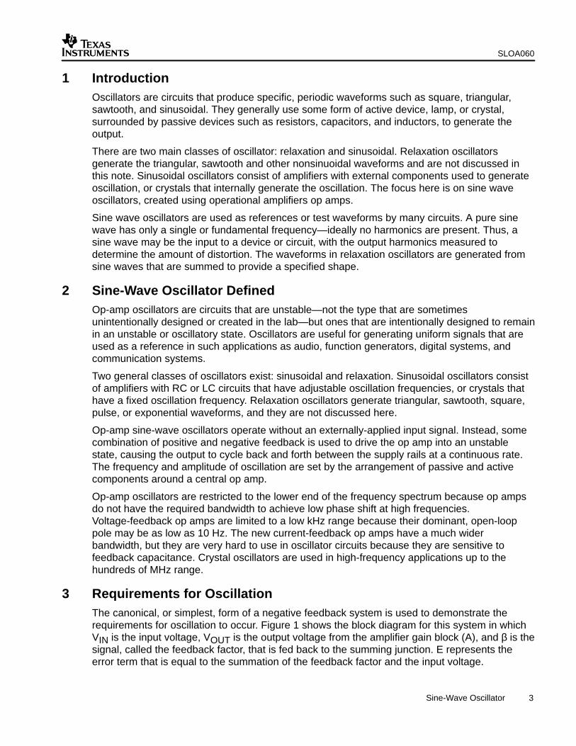
3 Requirements for OscillationThe canonical, or simplest, form of a negative feedback system is used to demonstrate therequirements for oscillation to occur. Figure 1 shows the block diagram for this system in whichVIN is the input voltage, VOUT is the output voltage from the amplifier gain block (A), and β is thesignal, called the feedback factor, that is fed back to the summing junction. E represents theerror term that is equal to the summation of the feedback factor and the input voltage.
SLOA060
4 Sine-Wave Oscillator
VOUTA
β
_ΣVIN
+ E
Figure 1. Canonical Form of a Feedback System With Positive or Negative Feedback
The corresponding classic expression for a feedback system is derived as follows. Equation 1 isthe defining equation for the output voltage; equation 2 is the corresponding error:
VOUT E A
E VIN VOUT
Eliminating the error term, E, from these equations gives
VOUT
A VIN–VOUT
and collecting the terms in VOUT yields
VIN VOUT1A Rearrangement of the terms produces equation 5, the classical form of feedback expression:
VOUT
VIN A
1 A
Oscillators do not require an externally-applied input signal; instead, they use some fraction ofthe output signal created by the feedback network as the input signal.
Oscillation results when the feedback system is not able to find a stable steady-state because itstransfer function can not be satisfied. The system goes unstable when the denominator inequation 5 becomes zero, i.e., when 1 + Aβ = 0, or Aβ = –1. The key to designing an oscillator isensuring that Aβ = –1. This is called the Barkhausen criterion. Satisfying this criterion requiresthat the magnitude of the loop gain is unity with a corresponding phase shift of 180 as indicatedby the minus sign. An equivalent expression using the symbology of complex algebra isAβ = 1∠ –180° for a negative feedback system. For a positive feedback system, the expressionis Aβ = 1∠ 0° and the sign of the Aβ term is negative in equation 5.
As the phase shift approaches 180° and |Aβ| → 1, the output voltage of the now-unstablesystem tends to infinity but, of course, is limited to finite values by an energy-limited powersupply. When the output voltage approaches either power rail, the active devices in theamplifiers change gain. This causes the value of A to change and forces Aβ away from thesingularity; thus the trajectory towards an infinite voltage slows and eventually halts. At thisstage, one of three things can occur: (i) Nonlinearity in saturation or cutoff causes the system tobecome stable and lock up at the current power rail. (ii) The initial change causes the system tosaturate (or cutoff) and stay that way for a long time before it becomes linear and heads for theopposite power rail. (iii) The system stays linear and reverses direction, heading for the oppositepower rail. The second alternative produces highly distorted oscillations (usually quasi-squarewaves), the resulting oscillators being called relaxation oscillators. The third produces asine-wave oscillator.
(1)
(2)
(3)
(4)
(5)
SLOA060
17 Sine-Wave Oscillator
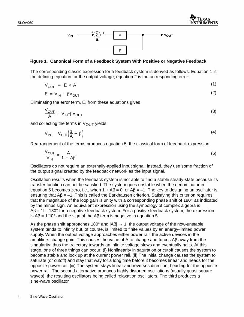
8.4 Bubba Oscillator
The bubba oscillator in Figure 18 is another phase-shift oscillator, but it takes advantage of thequad op-amp package to yield some unique advantages. Four RC sections require 45° phaseshift per section, so this oscillator has an excellent dφ/dt resulting in minimal frequency drift. TheRC sections each contribute 45° phase shift, so taking outputs from alternate sections yieldslow-impedance quadrature outputs. When an output is taken from each op amp, the circuitdelivers four 45 phase-shifted sine waves. The loop equation is given in equation 15. Whenω = 1/RCs, equation 15 reduces to equations 16 and 17.
A A 1RCs 1
4
| | 1
j 4
4
1
24 1
4
tan1(1) 45o
_
+
+5 V
VOUTSine
2.5 V
RG
360 kΩ
RF
1.5 MΩ
R
R
R
C
10 kΩ
10 kΩ
10 kΩ
10 nF
10 nF 10 nFCC
_+
_+
4/4 TLV2474
_+
VOUTCosine
10 nFC
R
10 kΩ
Figure 18. Bubba Oscillator
(15)
(16)
(17)
SLOA060
18 Sine-Wave Oscillator
Time = 500 µs/div
= 1
V/d
ivV O
UT
Figure 19. Output of the Circuit in Figure 18
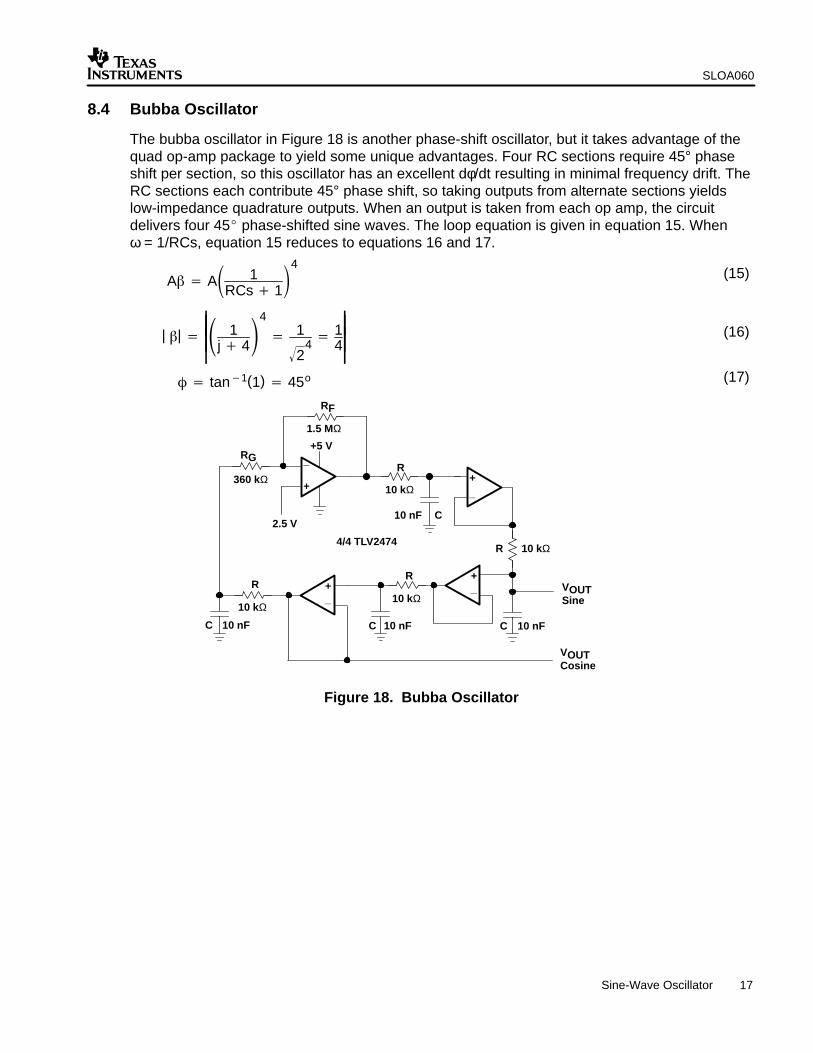
The gain, A, must equal 4 for oscillation to occur. The test circuit oscillated at 1.76 kHz ratherthan the ideal frequency of 1.72 kHz when the gain was 4.17 rather than the ideal gain of 4. Theoutput waveform is shown in Figure 19. Distortion was 1.1% for VOUTSINE and 0.1% forVOUTCOSINE. With low gain, A, and using low bias-current op amps, the gain-setting resistor, RG,did not load the last RC section, thus ensuring oscillator frequency accuracy. Very low distortionsine waves can be obtained from the junction of R and RG. When low-distortion sine waves arerequired at all outputs, the gain should be distributed among all the op amps. The noninvertinginput of the gain op amp is biased at 0.5 V to set the quiescent output voltage at 2.5 V forsingle-supply operation, and it should be ground for split-supply op amps. Gain distributionrequires biasing of the other op amps, but it has no effect on the oscillator frequency.
8.5 Quadrature Oscillator
The quadrature oscillator shown in Figure 20 is another type of phase-shift oscillator, but thethree RC sections are configured so each section contributes 90 of phase shift. This providesboth sine and cosine waveform outputs (the outputs are quadrature, or 90 apart), which is adistinct advantage over other phase-shift oscillators. The idea of the quadrature oscillator is touse the fact that the double integral of a sine wave is a negative sine wave of the samefrequency and phase, in other words, the original sine wave 180o phase shifted. The phase ofthe second integrator is then inverted and applied as positive feedback to induce oscillation [6].
The loop gain is calculated from equation 18. When R1C1 = R2C2 = R3C3, equation 18 reducesto equation 19. When ω = 1/RC, equation 18 reduces to 1∠ –180, so oscillation occurs atω = 2πf = 1/RC. The test circuit oscillated at 1.65 kHz rather than the calculated 1.59 kHz, asshown in Figure 21. This discrepancy is attributed to component variations. Both outputs haverelatively high distortion that can be reduced with a gain-stabilizing circuit. The sine output had0.846% distortion and the cosine output had 0.46% distortion. Adjusting the gain can increasethe amplitudes. The penalty is reduced bandwidth.
A A 1R1C1s
R3C3s 1
R3C3sR2C2s 1
(18)